EP3550388A1 - System and method for providing automation of microprocessor analog input stimulation - Google Patents
System and method for providing automation of microprocessor analog input stimulation Download PDFInfo
- Publication number
- EP3550388A1 EP3550388A1 EP19167068.6A EP19167068A EP3550388A1 EP 3550388 A1 EP3550388 A1 EP 3550388A1 EP 19167068 A EP19167068 A EP 19167068A EP 3550388 A1 EP3550388 A1 EP 3550388A1
- Authority
- EP
- European Patent Office
- Prior art keywords
- multiplexor
- spare
- sensor
- stimulation
- stimulation circuit
- Prior art date
- Legal status (The legal status is an assumption and is not a legal conclusion. Google has not performed a legal analysis and makes no representation as to the accuracy of the status listed.)
- Pending
Links
Images


Classifications
-
- G—PHYSICS
- G01—MEASURING; TESTING
- G01R—MEASURING ELECTRIC VARIABLES; MEASURING MAGNETIC VARIABLES
- G01R31/00—Arrangements for testing electric properties; Arrangements for locating electric faults; Arrangements for electrical testing characterised by what is being tested not provided for elsewhere
- G01R31/28—Testing of electronic circuits, e.g. by signal tracer
- G01R31/317—Testing of digital circuits
- G01R31/31723—Hardware for routing the test signal within the device under test to the circuits to be tested, e.g. multiplexer for multiple core testing, accessing internal nodes
-
- G—PHYSICS
- G05—CONTROLLING; REGULATING
- G05B—CONTROL OR REGULATING SYSTEMS IN GENERAL; FUNCTIONAL ELEMENTS OF SUCH SYSTEMS; MONITORING OR TESTING ARRANGEMENTS FOR SUCH SYSTEMS OR ELEMENTS
- G05B19/00—Program-control systems
- G05B19/02—Program-control systems electric
- G05B19/04—Program control other than numerical control, i.e. in sequence controllers or logic controllers
- G05B19/042—Program control other than numerical control, i.e. in sequence controllers or logic controllers using digital processors
- G05B19/0428—Safety, monitoring
-
- G—PHYSICS
- G01—MEASURING; TESTING
- G01R—MEASURING ELECTRIC VARIABLES; MEASURING MAGNETIC VARIABLES
- G01R31/00—Arrangements for testing electric properties; Arrangements for locating electric faults; Arrangements for electrical testing characterised by what is being tested not provided for elsewhere
- G01R31/28—Testing of electronic circuits, e.g. by signal tracer
- G01R31/317—Testing of digital circuits
- G01R31/31708—Analysis of signal quality
-
- G—PHYSICS
- G01—MEASURING; TESTING
- G01R—MEASURING ELECTRIC VARIABLES; MEASURING MAGNETIC VARIABLES
- G01R31/00—Arrangements for testing electric properties; Arrangements for locating electric faults; Arrangements for electrical testing characterised by what is being tested not provided for elsewhere
- G01R31/28—Testing of electronic circuits, e.g. by signal tracer
- G01R31/317—Testing of digital circuits
- G01R31/31712—Input or output aspects
-
- G—PHYSICS
- G05—CONTROLLING; REGULATING
- G05B—CONTROL OR REGULATING SYSTEMS IN GENERAL; FUNCTIONAL ELEMENTS OF SUCH SYSTEMS; MONITORING OR TESTING ARRANGEMENTS FOR SUCH SYSTEMS OR ELEMENTS
- G05B23/00—Testing or monitoring of control systems or parts thereof
- G05B23/02—Electric testing or monitoring
-
- G—PHYSICS
- G05—CONTROLLING; REGULATING
- G05B—CONTROL OR REGULATING SYSTEMS IN GENERAL; FUNCTIONAL ELEMENTS OF SUCH SYSTEMS; MONITORING OR TESTING ARRANGEMENTS FOR SUCH SYSTEMS OR ELEMENTS
- G05B23/00—Testing or monitoring of control systems or parts thereof
- G05B23/02—Electric testing or monitoring
- G05B23/0205—Electric testing or monitoring by means of a monitoring system capable of detecting and responding to faults
- G05B23/0218—Electric testing or monitoring by means of a monitoring system capable of detecting and responding to faults characterised by the fault detection method dealing with either existing or incipient faults
- G05B23/0256—Electric testing or monitoring by means of a monitoring system capable of detecting and responding to faults characterised by the fault detection method dealing with either existing or incipient faults injecting test signals and analyzing monitored process response, e.g. injecting the test signal while interrupting the normal operation of the monitored system; superimposing the test signal onto a control signal during normal operation of the monitored system
Definitions
- the present disclosure relates generally to microprocessor testing systems, and more specifically to a microprocessor including an automatic analog input stimulation for testing purposes.
- Controller systems such as those including microprocessors, frequently require analog inputs in order to perform the necessary control functions.
- a microprocessor may be configured to receive multiple signals from analog sensors, with the resultant controls being at least partially based on the received signals.
- microprocessors operate using digital data. In order to accommodate the analog signals, analog to digital converters are commonly used.
- various functionalities of the microprocessor are tested by providing a known analog input to a given input pin. This is commonly achieved through the usage of a stimulation circuit connected to an analog input and configured to cause the analog input to have a specific, predefined, value when the stimulation circuit is activated.
- operation and control of a stimulation circuit requires substantial software overhead by the microprocessor, and can limit the ability of the microprocessor to perform other tasks related to the controls.
- a controller system includes a microprocessor including a sequencer configured to output at least one spare multiplexor control signal, a memory, and plurality of sensor inputs, at least one stimulation circuit connected to a sensor signal line, the at least one stimulation circuit being connected to the at least one spare multiplexor control signal, and wherein the stimulation circuit is configured such that a state of the at least one spare multiplexor control signal controls a state of the stimulation circuit.
- the microprocessor further includes at least one analog to digital converter, and each of the sensor inputs in the plurality of sensor inputs is received at the analog to digital converter.
- controller systems further includes a multiplexor having a plurality of multiplexor sensor inputs and a multiplexed output, wherein the multiplexed output is received at one of the plurality of sensor inputs, and the sequencer is further configured to output at least one multiplexor control signal to the multiplexor.
- At least one stimulation circuit includes a first stimulation circuit connected to a sensor line connected to one of the multiplexor sensor inputs in the plurality of multiplexor sensor inputs.
- At least one stimulation circuit further includes a second stimulation circuit connected to a second sensor line, and the second sensor line is connected to one of the sensor inputs in the plurality of sensor inputs.
- At least one stimulation circuit is configured to operate as a passthrough circuit when the at least one spare multiplexor control signal is in a first state.
- At least one stimulation circuit is configured to drive the sensor signal to a first value when the at least one spare multiplexor control signal is in a second state, the second state being distinct from the first state.
- At least one spare multiplexor control signal includes a plurality of spare multiplexor control signals and the number of states in which the stimulation circuit is dependent on the quantity of spare multiplexor signals in the at least one spare multiplexor signal.
- At least one stimulation circuit comprises a plurality of stimulation circuits, each of the stimulation circuits being connected to a corresponding sensor signal line.
- each of the stimulation circuits in the plurality of stimulation circuits is controlled via the same spare multiplexor signal in the at least one spare multiplexor control signal.
- each of the stimulation circuits in the plurality of stimulation circuits is controlled via a distinct spare multiplexor signal in the at least one spare multiplexor control signal.
- each sensor signal line is connected to an aircraft sensor.
- An exemplary method for testing a microprocessor includes stimulating at least one sensor input via a stimulation circuit, wherein the stimulation circuit is controlled by at least one spare multiplexor signal output from a microprocessor sequencer, analyzing a response of the stimulated sensor input, and determining that at least one of a multiplexor and a conditioning circuit are healthy in response to the stimulated sensor input matching an expected stimulated sensor input.
- stimulating at least one sensor input comprises stimulating the sensor input for a duration of time at least as long as a circuit settling time.
- any of the above described exemplary methods for testing a microprocessor stimulating the at least one sensor input comprises providing a plurality of spare multiplexor signal outputs from the microprocessor sequencer to the stimulation circuit.
- any of the above described exemplary methods for testing a microprocessor stimulating the at least one sensor input comprises driving the sensor input to one of a plurality of predefined values, wherein the value is determined based on a high and low state of each of the spare multiplexor signals in the plurality of multiplexor signals.
- any of the above described exemplary methods for testing a microprocessor stimulating at least one sensor input via a stimulation circuit comprises engaging a first stimulation circuit via a first spare multiplexor signal output, and engaging a second stimulation circuit via a second spare multiplexor output signal.
- Another example of any of the above described exemplary methods for testing a microprocessor further includes operating the stimulation circuit as a pass through circuit when no control signal is output by the sequencer on the at least one spare multiplexor signal output.
- an aircraft control system includes a general aircraft controller, a plurality of dedicated systems controllers, each of the dedicated systems controllers including a microprocessor connected to a sensor network, each of the microprocessors includes a sequencer configured to output at least one spare multiplexor control signal, a memory, and plurality of sensor inputs, at least one stimulation circuit connected to a sensor signal line, the at least one stimulation circuit being connected to the at least one spare multiplexor control signal, and wherein the stimulation circuit is configured such that a state of the at least one spare multiplexor control signal controls a state of the stimulation circuit.
- FIG. 1 schematically illustrates an exemplary aircraft 10 including an electrical system 20 having a general aircraft controller 30.
- the general aircraft controller 30 is connected to multiple dedicated system controllers 40, each of which includes one or more microprocessors.
- the dedicated system controllers 40 are each connected to a corresponding sensor network 50 that includes one or more analog sensors configured to detect a characteristic of the system controlled by the corresponding dedicated system controller 40.
- the particular illustrated dedicated system controllers 40 are purely exemplary in nature, and a practical implementation could include any number of additional dedicated system controllers 40 and sensor networks 50, or less dedicated system controllers 40 and sensor networks 50, and still incorporate the testing system and method disclosed herein.
- each analog input at the microprocessor includes a sense circuit prior to the analog to digital conversion, and is conditioned to a proper voltage and noise filtering in order to be properly read by the microprocessor.
- the microprocessor within the dedicated system controller 40 includes a sequencer that outputs multiplexor control signals to the multiplexor and allows for the signals from the sensor network 50 to be multiplexed via the multiplexor. The multiplexing and conditioning allows the microprocessor to properly interpret the multiple signals, and to properly convert the multiple signals into a digital signal for storage and processing.
- One method used to ensure that the microprocessors within any given dedicated system controller 40 are operating correctly is to provide the microprocessor with a known preprogrammed value at a given sensor signal input and verify that the circuit is stimulated with the proper value.
- the method directs the sensor results to two different memory locations within the microcontroller, a first memory location with the stimulation circuit on and a second memory location with the stimulation circuit off.
- the microprocessor can then compare the value at the first memory location with an expected value of the stimulated input and determine whether the input conditioning and multiplexing is operating properly.
- the stimulation circuits can be controlled via multiplexor control signals output from a sequencer within the corresponding microprocessor.
- Figure 2 Schematically illustrates an exemplary control configuration for a controller system 100.
- the microprocessor 110 includes a sequencer 112 configured to output three multiplexor control signals 101, 103, 105.
- any number of multiplexor control signals 101, 103, 105 can be output by the sequencer 112 provided that the number of multiplexor control signals 101, 103, 105 is at least one greater than the total number of multiplexor signals 101, 103, 105 required to control any multiplexing of input signals.
- An analog to digital converter 114 is disposed at the signal inputs of the microprocessor 110 and converts any input signals into a digital form.
- the analog to digital converter 114 in the exemplary embodiment is a component of the microprocessor 110.
- the analog to digital converter 114 can be a distinct component from the microprocessor 110.
- the converted signals are then stored in a memory 116, with the particular memory address of each signal being determined by the input pin on which the signal was received and the specific state of the multiplexor output signals 101, 103, 105.
- the stimulation circuit 130 receives a multiplexor control signal 105 and, when not commanded to be active, the stimulation circuit 130 operates as a pass through with no impact on the received sensor signal 122.
- the exemplary multiplexor 140 is connected to two multiplexor control signals 101, 103 output from the sequencer 112.
- the two multiplexor control signals 101, 103 allow the multiplexor 140 to properly multiplex four distinct analog sensor signals 121, 123, 125, 127.
- a second stimulation circuit 132 is disposed at one of the signals 127 being multiplexed by the multiplexor 140, and is also connected to the multiplexor control signal 105 output from the sequencer 112.
- additional multiplexor control signals can be output from the sequencer 112 to the multiplexor 140, thereby allowing additional signals to be multiplexed by the multiplexor 140 according to known multiplexing techniques.
- the sequencer 112 can control the operation of the stimulation circuits 130, 132.
- one or more of the stimulation circuits 130, 132 can receive multiple inputs allowing for the analog input on the corresponding input line to be controlled to multiple distinct stimulated states.
- a stimulation circuit 130 receiving two multiplexor control signals can be operated in four different states as defined by the high/low state of the control signals (00, 01, 10 and 11). Each state results in a different operating point.
- the setting 00 may be normal with no stimulation, 01 a stimulation to the minimum condition, 10 a stimulation to a median condition, and 11 a stimulation to a maximum condition.
- the greater the number of spare multiplexor signals available the greater the number of states that a connected stimulation circuit 130, 132 can be driven to.
- the number of stimulation states can be expanded by expanding the number of multiplexor control signals utilized to control the stimulation circuit.
- the amount of software overhead required to operate the stimulation circuits 130, 132 and test the microprocessor 110 is reduced.
- the reduced software overhead occurs because the sequencer progresses through all of the necessary multiplexor settings while automatically controlling the analog to digital converter and placing the resulting values into the processors RAM. This allows the software to read the most recent value for all conditions (normal and each stimulation setting) at any time without the overhead of controlling the stimulation and analog to digital converter.
- Figure 3 illustrates a method for self-testing a microprocessor 110 in the controller system 100 of Figure 2 .
- the microprocessor 110 outputs a multiplexor control signal on the spare multiplexor control signal line 105 that is connected to one or more stimulation circuits 130, 132 in a "Stimulate Analog Input" step 210 using the sequencer 112.
- the multiplexor control signal causes the connected stimulation circuit 130, 132 to stimulate the corresponding analog input, driving the input value to a predetermined stimulation value.
- the particular combination of multiplexor control signal values determines the level of stimulation applied to the corresponding analog input line in the manner described above.
- the microprocessor 110 waits a predefined time period, to allow the circuit output to transition to the new value before creating the analog to digital converted value to be used by the microprocessor. This can be referred to as waiting a duration equal to the settling time of the circuit after adjusting the stimulating setting.
- the microprocessor 110 analyzes the reactions of the microprocessor 110 in an "Analyze Microprocessor Reactions" step 220.
- the microprocessor is healthy (e.g. in full working order)
- the predefined inputs resulting from the stimulated analog inputs will define a known microprocessor output or reaction.
- the microprocessor 110, or other controller compares the actual reactions of the microprocessor 110 to the expected reactions. Once the comparison has been made, the microprocessor 110, or other controller, determines the health of the microprocessor 110 in a "Determine Health of Microprocessor" step 230.
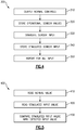
- Figure 4 illustrates a method 300 for generating stimulated input values for each input of the microprocessor 110 of Figure 2 .
- the standard operational controls are output from the microprocessor 110 on the utilized multiplexor control lines 101, 103 and the spare multiplexor control line 105 in an "Output Normal Controls" step 310.
- the resultant sensor signals are processed through the analog to digital converter 114, and stored in a second memory location in an "Store Operational Sensor Values" step 320.
- the microprocessor 110 outputs a stimulation signal on the spare multiplexer control line(s) 105, and the standard multiplexor controls on the utilized multiplexor control lines 101, 103 in a "Stimulate Sensor Input” step 330.
- the sensor input is passed through the analog to digital converter, and the multiplexor where appropriate, and stored in the first memory location in a "Store Stimulated Sensor Input” step 340. This process is then re-iterated for all of the sensor inputs at the microprocessor 110 in a "Repeat For All Sensor Inputs" step 350.
- Figure 5 schematically illustrates a method 400 for determining the health of a given input utilizing the stimulated sensor input value determined through the method 300 of Figure 4 .
- the microprocessor 110 reads the normal value of the sensor input from the second memory location in a "Read Normal Value” step 410.
- the normal value is used for microprocessor 110 control operations.
- the microprocessor reads the stimulated input value from the first memory location in a "Read Stimulated Input Value" step 420.
- the microprocessor 110 compares the stimulated input value with an expected stimulated value for the given stimulation conditions in a "Compare Stimulated Input Value With Expected Input Value" step 430. If the comparison reveals that the stimulated input value and the expected input value are within tolerance of each other, the microprocessor determines that the conditioning circuitry, analog to digital converter, and the multiplexor 140 (if present) are healthy. Otherwise, the microprocessor 110 determines that at least one of the conditioning circuitry, analog to digital converter, and the multiplexor 140 (if present) is unhealthy, and the microprocessor 110 can move to take any corresponding action.
- the microprocessor 110 can reiterate the process for any or all sensor inputs which include a stimulated sensor input value, and the health of any corresponding input circuitry can be determined. In this way, the health of each individual sensor input can be determined.
Landscapes
- Physics & Mathematics (AREA)
- Engineering & Computer Science (AREA)
- General Physics & Mathematics (AREA)
- General Engineering & Computer Science (AREA)
- Automation & Control Theory (AREA)
- Computer Networks & Wireless Communication (AREA)
- Nonlinear Science (AREA)
- Safety Devices In Control Systems (AREA)
Abstract
Description
- The present disclosure relates generally to microprocessor testing systems, and more specifically to a microprocessor including an automatic analog input stimulation for testing purposes.
- Controller systems, such as those including microprocessors, frequently require analog inputs in order to perform the necessary control functions. By way of example, a microprocessor may be configured to receive multiple signals from analog sensors, with the resultant controls being at least partially based on the received signals. However, as is generally known in the art, microprocessors operate using digital data. In order to accommodate the analog signals, analog to digital converters are commonly used.
- Further, in some systems various functionalities of the microprocessor are tested by providing a known analog input to a given input pin. This is commonly achieved through the usage of a stimulation circuit connected to an analog input and configured to cause the analog input to have a specific, predefined, value when the stimulation circuit is activated. However, in existing controllers operation and control of a stimulation circuit requires substantial software overhead by the microprocessor, and can limit the ability of the microprocessor to perform other tasks related to the controls.
- In one exemplary embodiment a controller system includes a microprocessor including a sequencer configured to output at least one spare multiplexor control signal, a memory, and plurality of sensor inputs, at least one stimulation circuit connected to a sensor signal line, the at least one stimulation circuit being connected to the at least one spare multiplexor control signal, and wherein the stimulation circuit is configured such that a state of the at least one spare multiplexor control signal controls a state of the stimulation circuit.
- In another example of the above described controller system the microprocessor further includes at least one analog to digital converter, and each of the sensor inputs in the plurality of sensor inputs is received at the analog to digital converter.
- Another example of any of the above described controller systems further includes a multiplexor having a plurality of multiplexor sensor inputs and a multiplexed output, wherein the multiplexed output is received at one of the plurality of sensor inputs, and the sequencer is further configured to output at least one multiplexor control signal to the multiplexor.
- In another example of any of the above described controller systems where at least one stimulation circuit includes a first stimulation circuit connected to a sensor line connected to one of the multiplexor sensor inputs in the plurality of multiplexor sensor inputs.
- In another example of any of the above described controller systems where at least one stimulation circuit further includes a second stimulation circuit connected to a second sensor line, and the second sensor line is connected to one of the sensor inputs in the plurality of sensor inputs.
- In another example of any of the above described controller systems where at least one stimulation circuit is configured to operate as a passthrough circuit when the at least one spare multiplexor control signal is in a first state.
- In another example of any of the above described controller systems where at least one stimulation circuit is configured to drive the sensor signal to a first value when the at least one spare multiplexor control signal is in a second state, the second state being distinct from the first state.
- In another example of any of the above described controller systems where at least one spare multiplexor control signal includes a plurality of spare multiplexor control signals and the number of states in which the stimulation circuit is dependent on the quantity of spare multiplexor signals in the at least one spare multiplexor signal.
- In another example of any of the above described controller systems where at least one stimulation circuit comprises a plurality of stimulation circuits, each of the stimulation circuits being connected to a corresponding sensor signal line.
- In another example of any of the above described controller systems each of the stimulation circuits in the plurality of stimulation circuits is controlled via the same spare multiplexor signal in the at least one spare multiplexor control signal.
- In another example of any of the above described controller systems each of the stimulation circuits in the plurality of stimulation circuits is controlled via a distinct spare multiplexor signal in the at least one spare multiplexor control signal.
- In another example of any of the above described controller systems each sensor signal line is connected to an aircraft sensor.
- An exemplary method for testing a microprocessor includes stimulating at least one sensor input via a stimulation circuit, wherein the stimulation circuit is controlled by at least one spare multiplexor signal output from a microprocessor sequencer, analyzing a response of the stimulated sensor input, and determining that at least one of a multiplexor and a conditioning circuit are healthy in response to the stimulated sensor input matching an expected stimulated sensor input.
- In another example of the above described exemplary method for testing a microprocessor stimulating at least one sensor input comprises stimulating the sensor input for a duration of time at least as long as a circuit settling time.
- In another example of any of the above described exemplary methods for testing a microprocessor stimulating the at least one sensor input comprises providing a plurality of spare multiplexor signal outputs from the microprocessor sequencer to the stimulation circuit.
- In another example of any of the above described exemplary methods for testing a microprocessor stimulating the at least one sensor input comprises driving the sensor input to one of a plurality of predefined values, wherein the value is determined based on a high and low state of each of the spare multiplexor signals in the plurality of multiplexor signals.
- In another example of any of the above described exemplary methods for testing a microprocessor stimulating at least one sensor input via a stimulation circuit comprises engaging a first stimulation circuit via a first spare multiplexor signal output, and engaging a second stimulation circuit via a second spare multiplexor output signal.
- Another example of any of the above described exemplary methods for testing a microprocessor further includes operating the stimulation circuit as a pass through circuit when no control signal is output by the sequencer on the at least one spare multiplexor signal output.
- In one exemplary embodiment an aircraft control system includes a general aircraft controller, a plurality of dedicated systems controllers, each of the dedicated systems controllers including a microprocessor connected to a sensor network, each of the microprocessors includes a sequencer configured to output at least one spare multiplexor control signal, a memory, and plurality of sensor inputs, at least one stimulation circuit connected to a sensor signal line, the at least one stimulation circuit being connected to the at least one spare multiplexor control signal, and wherein the stimulation circuit is configured such that a state of the at least one spare multiplexor control signal controls a state of the stimulation circuit.
- These and other features of the present invention can be best understood from the following specification and drawings, the following of which is a brief description.
-
-
Figure 1 schematically illustrates an exemplary aircraft including multiple controllers distributed throughout the aircraft. -
Figure 2 schematically illustrates a controller configuration according to one example. -
Figure 3 illustrates a method of operating the control configuration ofFigure 2 in order to provide a test value to at least one controller input. -
Figure 4 illustrates a method of generating a stimulated input value for each input to a microprocessor within the controller configuration ofFigure 2 . -
Figure 5 illustrates a method for verifying the health of each input of the controller configuration ofFigure 2 . -
Figure 1 schematically illustrates anexemplary aircraft 10 including anelectrical system 20 having ageneral aircraft controller 30. Thegeneral aircraft controller 30 is connected to multiplededicated system controllers 40, each of which includes one or more microprocessors. Thededicated system controllers 40 are each connected to acorresponding sensor network 50 that includes one or more analog sensors configured to detect a characteristic of the system controlled by the correspondingdedicated system controller 40. It should be appreciated that the particular illustrateddedicated system controllers 40 are purely exemplary in nature, and a practical implementation could include any number of additionaldedicated system controllers 40 andsensor networks 50, or lessdedicated system controllers 40 andsensor networks 50, and still incorporate the testing system and method disclosed herein. - In order to accommodate the multiple analog inputs from the
sensor network 50, a multiplexor is included that combines multiple analog inputs into a single input for the microprocessor. In general, each analog input at the microprocessor includes a sense circuit prior to the analog to digital conversion, and is conditioned to a proper voltage and noise filtering in order to be properly read by the microprocessor. The microprocessor within thededicated system controller 40 includes a sequencer that outputs multiplexor control signals to the multiplexor and allows for the signals from thesensor network 50 to be multiplexed via the multiplexor. The multiplexing and conditioning allows the microprocessor to properly interpret the multiple signals, and to properly convert the multiple signals into a digital signal for storage and processing. - One method used to ensure that the microprocessors within any given
dedicated system controller 40 are operating correctly is to provide the microprocessor with a known preprogrammed value at a given sensor signal input and verify that the circuit is stimulated with the proper value. The method directs the sensor results to two different memory locations within the microcontroller, a first memory location with the stimulation circuit on and a second memory location with the stimulation circuit off. The microprocessor can then compare the value at the first memory location with an expected value of the stimulated input and determine whether the input conditioning and multiplexing is operating properly. In order to reduce the software overhead required to operate the stimulation circuits, the stimulation circuits can be controlled via multiplexor control signals output from a sequencer within the corresponding microprocessor. - With continued reference to
Figure 1 ,Figure 2 Schematically illustrates an exemplary control configuration for acontroller system 100. Included within thecontroller system 100 is amicroprocessor 110. Themicroprocessor 110 includes asequencer 112 configured to output threemultiplexor control signals multiplexor control signals sequencer 112 provided that the number ofmultiplexor control signals multiplexor signals digital converter 114 is disposed at the signal inputs of themicroprocessor 110 and converts any input signals into a digital form. The analog todigital converter 114 in the exemplary embodiment is a component of themicroprocessor 110. In alternative embodiments, the analog todigital converter 114 can be a distinct component from themicroprocessor 110. The converted signals are then stored in amemory 116, with the particular memory address of each signal being determined by the input pin on which the signal was received and the specific state of themultiplexor output signals - Connected to two of the input pins are direct
analog sensor signals 120. Connected to a third input pin is a third directanalog sensor signal 122. The third directanalog sensor signal 122 is passed through astimulation circuit 130. Thestimulation circuit 130 receives amultiplexor control signal 105 and, when not commanded to be active, thestimulation circuit 130 operates as a pass through with no impact on the receivedsensor signal 122. - Connected to a fourth input pin is an output of a
multiplexor 140. Theexemplary multiplexor 140 is connected to twomultiplexor control signals sequencer 112. The twomultiplexor control signals multiplexor 140 to properly multiplex four distinctanalog sensor signals second stimulation circuit 132 is disposed at one of thesignals 127 being multiplexed by themultiplexor 140, and is also connected to the multiplexor control signal 105 output from thesequencer 112. In alternative examples, additional multiplexor control signals can be output from thesequencer 112 to themultiplexor 140, thereby allowing additional signals to be multiplexed by themultiplexor 140 according to known multiplexing techniques. - By utilizing a spare multiplexor control signal 105 (i.e. a multiplexor control signal 105 that is not required to control the multiplexor 140), the
sequencer 112 can control the operation of thestimulation circuits stimulation circuits stimulation circuit 130 receiving two multiplexor control signals can be operated in four different states as defined by the high/low state of the control signals (00, 01, 10 and 11). Each state results in a different operating point. For example, the setting 00 may be normal with no stimulation, 01 a stimulation to the minimum condition, 10 a stimulation to a median condition, and 11 a stimulation to a maximum condition. As can be appreciated, the greater the number of spare multiplexor signals available, the greater the number of states that aconnected stimulation circuit - By utilizing spare
multiplexor outputs 105 from thesequencer 112 to control thestimulation circuits stimulation circuits microprocessor 110 is reduced. The reduced software overhead occurs because the sequencer progresses through all of the necessary multiplexor settings while automatically controlling the analog to digital converter and placing the resulting values into the processors RAM. This allows the software to read the most recent value for all conditions (normal and each stimulation setting) at any time without the overhead of controlling the stimulation and analog to digital converter. - With continued reference to
Figures 1 and2, Figure 3 illustrates a method for self-testing amicroprocessor 110 in thecontroller system 100 ofFigure 2 . Initially, themicroprocessor 110 outputs a multiplexor control signal on the spare multiplexorcontrol signal line 105 that is connected to one ormore stimulation circuits step 210 using thesequencer 112. The multiplexor control signal causes theconnected stimulation circuit - In examples where multiple spare multiplexor control signal lines are connected to any given stimulation circuit, the particular combination of multiplexor control signal values determines the level of stimulation applied to the corresponding analog input line in the manner described above. Once the stimulation is turned on or off, the
microprocessor 110 waits a predefined time period, to allow the circuit output to transition to the new value before creating the analog to digital converted value to be used by the microprocessor. This can be referred to as waiting a duration equal to the settling time of the circuit after adjusting the stimulating setting. - In some examples, once the
stimulation circuits 130, 32 have been applied for a sufficient duration to ensure the expected reaction from themicroprocessor 110, themicroprocessor 110, or another controller within the system, analyzes the reactions of themicroprocessor 110 in an "Analyze Microprocessor Reactions"step 220. When the microprocessor is healthy (e.g. in full working order), the predefined inputs resulting from the stimulated analog inputs will define a known microprocessor output or reaction. During the analyze microprocessor reactions step 220, themicroprocessor 110, or other controller, compares the actual reactions of themicroprocessor 110 to the expected reactions. Once the comparison has been made, themicroprocessor 110, or other controller, determines the health of themicroprocessor 110 in a "Determine Health of Microprocessor"step 230. - With continued reference to
Figures 1-3 ,Figure 4 illustrates amethod 300 for generating stimulated input values for each input of themicroprocessor 110 ofFigure 2 . Initially, the standard operational controls are output from themicroprocessor 110 on the utilizedmultiplexor control lines multiplexor control line 105 in an "Output Normal Controls"step 310. The resultant sensor signals are processed through the analog todigital converter 114, and stored in a second memory location in an "Store Operational Sensor Values"step 320. - Once the normal operational values have been stored, the
microprocessor 110 outputs a stimulation signal on the spare multiplexer control line(s) 105, and the standard multiplexor controls on the utilizedmultiplexor control lines step 330. Once stimulated, the sensor input is passed through the analog to digital converter, and the multiplexor where appropriate, and stored in the first memory location in a "Store Stimulated Sensor Input"step 340. This process is then re-iterated for all of the sensor inputs at themicroprocessor 110 in a "Repeat For All Sensor Inputs"step 350. - With continued reference to
Figures 1-4 ,Figure 5 schematically illustrates amethod 400 for determining the health of a given input utilizing the stimulated sensor input value determined through themethod 300 ofFigure 4 . Initially, themicroprocessor 110 reads the normal value of the sensor input from the second memory location in a "Read Normal Value"step 410. The normal value is used formicroprocessor 110 control operations. Next, the microprocessor reads the stimulated input value from the first memory location in a "Read Stimulated Input Value"step 420. - The
microprocessor 110 then compares the stimulated input value with an expected stimulated value for the given stimulation conditions in a "Compare Stimulated Input Value With Expected Input Value"step 430. If the comparison reveals that the stimulated input value and the expected input value are within tolerance of each other, the microprocessor determines that the conditioning circuitry, analog to digital converter, and the multiplexor 140 (if present) are healthy. Otherwise, themicroprocessor 110 determines that at least one of the conditioning circuitry, analog to digital converter, and the multiplexor 140 (if present) is unhealthy, and themicroprocessor 110 can move to take any corresponding action. - While described in
Figure 5 as a process for an individual sensor input, themicroprocessor 110 can reiterate the process for any or all sensor inputs which include a stimulated sensor input value, and the health of any corresponding input circuitry can be determined. In this way, the health of each individual sensor input can be determined. - While described above with regards to a microprocessor controller within a
control system 20 of an aircraft, it is understood that the system and method can be applied to any digital controller including a microprocessor and receiving analog inputs and is not limited to aircraft applications. - It is further understood that any of the above described concepts can be used alone or in combination with any or all of the other above described concepts. Although an embodiment of this invention has been disclosed, a worker of ordinary skill in this art would recognize that certain modifications would come within the scope of this invention as defined by the claims. For that reason, the following claims should be studied to determine the true scope of this invention.
Claims (15)
- A controller system comprising:a microprocessor (110) including a sequencer (112) configured to output at least one spare multiplexor control signal, a memory (116), and plurality of sensor inputs;at least one stimulation circuit (130) connected to a sensor signal line, the at least one stimulation circuit being connected to the at least one spare multiplexor control signal; andwherein the stimulation circuit (130) is configured such that a state of the at least one spare multiplexor control signal controls a state of the stimulation circuit.
- The controller system of claim 1, wherein the microprocessor further includes at least one analog to digital converter (114), and each of the sensor inputs in the plurality of sensor inputs is received at the analog to digital converter.
- The controller system of claim 1 or 2, further comprising a multiplexor (140) having a plurality of multiplexor sensor inputs and a multiplexed output, wherein the multiplexed output is received at one of the plurality of sensor inputs, and the sequencer is further configured to output at least one multiplexor control signal to the multiplexor.
- The controller system of claim 3, wherein the at least one stimulation circuit includes a first stimulation circuit connected to a sensor line connected to one of the multiplexor sensor inputs in the plurality of multiplexor sensor inputs.
- The controller system of claim 4, wherein the at least one stimulation circuit further includes a second stimulation circuit connected to a second sensor line, and the second sensor line is connected to one of the sensor inputs in the plurality of sensor inputs.
- The controller system of any preceding claim, wherein the at least one stimulation circuit is configured to operate as a passthrough circuit when the at least one spare multiplexor control signal is in a first state.
- The controller system of claim 6, wherein the at least one stimulation circuit is configured to drive the sensor signal to a first value when the at least one spare multiplexor control signal is in a second state, the second state being distinct from the first state.
- The controller system of claim 6, wherein the at least one spare multiplexor control signal includes a plurality of spare multiplexor control signals and the number of states in which the stimulation circuit is dependent on the quantity of spare multiplexor signals in the at least one spare multiplexor signal.
- The controller system of any preceding claim, wherein the at least one stimulation circuit comprises a plurality of stimulation circuits, each of the stimulation circuits being connected to a corresponding sensor signal line, and preferably wherein each of the stimulation circuits in the plurality of stimulation circuits is controlled via the same spare multiplexor signal in the at least one spare multiplexor control signal, or wherein each of the stimulation circuits in the plurality of stimulation circuits is controlled via a distinct spare multiplexor signal in the at least one spare multiplexor control signal.
- The controller system of claim 1, wherein each sensor signal line is connected to an aircraft sensor.
- A method for testing a microprocessor comprising:stimulating at least one sensor input via a stimulation circuit, wherein the stimulation circuit is controlled by at least one spare multiplexor signal output from a microprocessor sequencer;analyzing a response of the stimulated sensor input; anddetermining that at least one of a multiplexor and a conditioning circuit are healthy in response to the stimulated sensor input matching an expected stimulated sensor input.
- The method of claim 11, wherein stimulating at least one sensor input comprises stimulating the sensor input for a duration of time at least as long as a circuit settling time.
- The method of claim 11 or 12, wherein stimulating the at least one sensor input comprises providing a plurality of spare multiplexor signal outputs from the microprocessor sequencer to the stimulation circuit, and preferably wherein stimulating the at least one sensor input comprises driving the sensor input to one of a plurality of predefined values, wherein the value is determined based on a high and low state of each of the spare multiplexor signals in the plurality of multiplexor signals; or wherein stimulating at least one sensor input via a stimulation circuit comprises engaging a first stimulation circuit via a first spare multiplexor signal output, and engaging a second stimulation circuit via a second spare multiplexor output signal.
- The method of claim 11, 12 or 13, further comprising operating the stimulation circuit as a pass through circuit when no control signal is output by the sequencer on the at least one spare multiplexor signal output.
- An aircraft control system comprising:a general aircraft controller (30);a plurality of dedicated systems controllers (40), each of said dedicated systems controllers including a microprocessor (110) connected to a sensor network;each of the microprocessors includes a sequencer configured to output at least one spare multiplexor control signal, a memory (116), and plurality of sensor inputs, at least one stimulation circuit (130) connected to a sensor signal line, the at least one stimulation circuit being connected to the at least one spare multiplexor control signal, and wherein the stimulation circuit is configured such that a state of the at least one spare multiplexor control signal controls a state of the stimulation circuit.
Applications Claiming Priority (1)
| Application Number | Priority Date | Filing Date | Title |
|---|---|---|---|
| US15/943,871 US10613143B2 (en) | 2018-04-03 | 2018-04-03 | System and method for providing automation of microprocessor analog input stimulation |
Publications (1)
| Publication Number | Publication Date |
|---|---|
| EP3550388A1 true EP3550388A1 (en) | 2019-10-09 |
Family
ID=66092066
Family Applications (1)
| Application Number | Title | Priority Date | Filing Date |
|---|---|---|---|
| EP19167068.6A Pending EP3550388A1 (en) | 2018-04-03 | 2019-04-03 | System and method for providing automation of microprocessor analog input stimulation |
Country Status (2)
| Country | Link |
|---|---|
| US (1) | US10613143B2 (en) |
| EP (1) | EP3550388A1 (en) |
Citations (3)
| Publication number | Priority date | Publication date | Assignee | Title |
|---|---|---|---|---|
| US4155116A (en) * | 1978-01-04 | 1979-05-15 | The Bendix Corporation | Digital control system including built in test equipment |
| US5638383A (en) * | 1992-07-24 | 1997-06-10 | Trw Inc. | Advanced integrated avionics testing system |
| WO2015116469A1 (en) * | 2014-01-29 | 2015-08-06 | General Electric Company | System and method for verifying the configuration and installation of a monitoring and protection system |
Family Cites Families (8)
| Publication number | Priority date | Publication date | Assignee | Title |
|---|---|---|---|---|
| US4044244A (en) | 1976-08-06 | 1977-08-23 | International Business Machines Corporation | Automatic tester for complex semiconductor components including combinations of logic, memory and analog devices and processes of testing thereof |
| FR2567273B1 (en) * | 1984-07-03 | 1986-11-14 | Commissariat Energie Atomique | DEVICE FOR SIMULATING THE FAILURE OR THE PROPER FUNCTIONING OF A LOGIC SYSTEM |
| US5640509A (en) | 1995-10-03 | 1997-06-17 | Intel Corporation | Programmable built-in self-test function for an integrated circuit |
| US5946472A (en) * | 1996-10-31 | 1999-08-31 | International Business Machines Corporation | Apparatus and method for performing behavioral modeling in hardware emulation and simulation environments |
| US6486809B1 (en) | 1999-06-02 | 2002-11-26 | Texas Instruments Incorporated | Analog to digital converter with configurable sequence controller |
| US6559783B1 (en) | 2000-08-16 | 2003-05-06 | Microchip Technology Incorporated | Programmable auto-converting analog to digital conversion module |
| DE102006008539A1 (en) * | 2006-02-22 | 2007-08-30 | Robert Bosch Gmbh | Error condition simulating method for use in control device, involves connecting circuit points of device to be tested with points of fault generation circuit across multiplexer, and multiplexer is implemented using relay technology |
| US9618933B2 (en) * | 2014-02-10 | 2017-04-11 | General Electric Company | System and method for verifying the configuration and installation of a monitoring and protection system |
-
2018
- 2018-04-03 US US15/943,871 patent/US10613143B2/en active Active
-
2019
- 2019-04-03 EP EP19167068.6A patent/EP3550388A1/en active Pending
Patent Citations (3)
| Publication number | Priority date | Publication date | Assignee | Title |
|---|---|---|---|---|
| US4155116A (en) * | 1978-01-04 | 1979-05-15 | The Bendix Corporation | Digital control system including built in test equipment |
| US5638383A (en) * | 1992-07-24 | 1997-06-10 | Trw Inc. | Advanced integrated avionics testing system |
| WO2015116469A1 (en) * | 2014-01-29 | 2015-08-06 | General Electric Company | System and method for verifying the configuration and installation of a monitoring and protection system |
Also Published As
| Publication number | Publication date |
|---|---|
| US10613143B2 (en) | 2020-04-07 |
| US20190302182A1 (en) | 2019-10-03 |
Similar Documents
| Publication | Publication Date | Title |
|---|---|---|
| EP0136205B1 (en) | Method and apparatus for applying and monitoring programmed test signals during automated testing of electronic circuits | |
| EP0322141A2 (en) | Dual computer cross-checking system | |
| DE10334801B3 (en) | Semiconductor circuit for exchanging external data, addresses and/or commands during normal operation has a test interface for a test operation with a built-in self-test | |
| DE102012023350B4 (en) | Systems, circuits and a method for generating configurable feedback | |
| DE102014109009A1 (en) | Multi-phase controller with self-test | |
| EP1857827B1 (en) | Circuit device with serial test interface and serial test mode procedure | |
| WO2011088893A1 (en) | Method and apparatus for testing a device-under-test | |
| CN115128429A (en) | Chip testing system and testing method thereof | |
| KR20210046390A (en) | AUTOSAR BSW testing automation system and testing method thereof | |
| US10613143B2 (en) | System and method for providing automation of microprocessor analog input stimulation | |
| US20040217385A1 (en) | Arrangement consisting of a program-controlled unit and a power chip connected to it | |
| EP2786162B1 (en) | Method of detecting a fault in connecting lines between a central unit and a plurality of electronic components which are independent of one another | |
| DE102013107908B4 (en) | Circuit arrangements and methods for receiving information | |
| US7269488B2 (en) | Method for controlling a component of a distributed safety-relevant system | |
| JP4648453B2 (en) | System and method for testing a controller mechanism | |
| US6650950B2 (en) | Method for monitoring an output unit | |
| EP0281620B1 (en) | Apparatus and method for testing an equipment and stimulating apparatus | |
| RU2250565C2 (en) | Computer-based instrumentation | |
| JP2551939B2 (en) | IC test equipment | |
| EP2394865B1 (en) | Method and device for diagnosing the functioning of an energy supply device | |
| CN112505520B (en) | Chip testing method, device and system | |
| EP0293261B1 (en) | Digital in-circuit tester having channel-memory erase-preventer | |
| US20110161906A1 (en) | Signal conversion facility and method for creating programming for a signal conversion facility | |
| CN111123140A (en) | time division method | |
| EP3151022B1 (en) | Duty cycle-based bit interface system |
Legal Events
| Date | Code | Title | Description |
|---|---|---|---|
| PUAI | Public reference made under article 153(3) epc to a published international application that has entered the european phase |
Free format text: ORIGINAL CODE: 0009012 |
|
| STAA | Information on the status of an ep patent application or granted ep patent |
Free format text: STATUS: THE APPLICATION HAS BEEN PUBLISHED |
|
| AK | Designated contracting states |
Kind code of ref document: A1 Designated state(s): AL AT BE BG CH CY CZ DE DK EE ES FI FR GB GR HR HU IE IS IT LI LT LU LV MC MK MT NL NO PL PT RO RS SE SI SK SM TR |
|
| AX | Request for extension of the european patent |
Extension state: BA ME |
|
| STAA | Information on the status of an ep patent application or granted ep patent |
Free format text: STATUS: REQUEST FOR EXAMINATION WAS MADE |
|
| 17P | Request for examination filed |
Effective date: 20191216 |
|
| RBV | Designated contracting states (corrected) |
Designated state(s): AL AT BE BG CH CY CZ DE DK EE ES FI FR GB GR HR HU IE IS IT LI LT LU LV MC MK MT NL NO PL PT RO RS SE SI SK SM TR |
|
| STAA | Information on the status of an ep patent application or granted ep patent |
Free format text: STATUS: EXAMINATION IS IN PROGRESS |
|
| 17Q | First examination report despatched |
Effective date: 20201125 |
|
| GRAP | Despatch of communication of intention to grant a patent |
Free format text: ORIGINAL CODE: EPIDOSNIGR1 |
|
| STAA | Information on the status of an ep patent application or granted ep patent |
Free format text: STATUS: GRANT OF PATENT IS INTENDED |
|
| INTG | Intention to grant announced |
Effective date: 20251222 |
|
| GRAS | Grant fee paid |
Free format text: ORIGINAL CODE: EPIDOSNIGR3 |
|
| GRAA | (expected) grant |
Free format text: ORIGINAL CODE: 0009210 |
|
| STAA | Information on the status of an ep patent application or granted ep patent |
Free format text: STATUS: THE PATENT HAS BEEN GRANTED |