EP3549701A1 - Surface-coated cutting tool - Google Patents
Surface-coated cutting tool Download PDFInfo
- Publication number
- EP3549701A1 EP3549701A1 EP17876785.1A EP17876785A EP3549701A1 EP 3549701 A1 EP3549701 A1 EP 3549701A1 EP 17876785 A EP17876785 A EP 17876785A EP 3549701 A1 EP3549701 A1 EP 3549701A1
- Authority
- EP
- European Patent Office
- Prior art keywords
- layers
- thickness
- area
- layer
- multilayer
- Prior art date
- Legal status (The legal status is an assumption and is not a legal conclusion. Google has not performed a legal analysis and makes no representation as to the accuracy of the status listed.)
- Pending
Links
- 238000005520 cutting process Methods 0.000 title claims abstract description 71
- 239000000463 material Substances 0.000 claims abstract description 114
- 239000011248 coating agent Substances 0.000 claims abstract description 62
- 238000000576 coating method Methods 0.000 claims abstract description 62
- 239000000203 mixture Substances 0.000 claims abstract description 31
- 238000010276 construction Methods 0.000 claims abstract description 19
- 229910052757 nitrogen Inorganic materials 0.000 claims abstract description 14
- 229910052782 aluminium Inorganic materials 0.000 claims abstract description 13
- 229910052719 titanium Inorganic materials 0.000 claims abstract description 10
- 229910052804 chromium Inorganic materials 0.000 claims abstract description 9
- 229910052710 silicon Inorganic materials 0.000 claims abstract description 9
- 229910052799 carbon Inorganic materials 0.000 claims abstract description 6
- 229910052758 niobium Inorganic materials 0.000 claims abstract description 6
- 229910052715 tantalum Inorganic materials 0.000 claims abstract description 6
- 229910052721 tungsten Inorganic materials 0.000 claims abstract description 6
- 150000001875 compounds Chemical class 0.000 claims description 9
- 239000010410 layer Substances 0.000 description 611
- 239000010936 titanium Substances 0.000 description 50
- 238000000151 deposition Methods 0.000 description 23
- 230000008021 deposition Effects 0.000 description 22
- 238000000034 method Methods 0.000 description 18
- 230000007423 decrease Effects 0.000 description 16
- 238000012360 testing method Methods 0.000 description 14
- 239000002344 surface layer Substances 0.000 description 12
- 230000003247 decreasing effect Effects 0.000 description 11
- SSJWWCKNRIUXON-UHFFFAOYSA-N 2-(2,6-dimethoxyphenyl)-5-hydroxy-7,8-dimethoxychromen-4-one Chemical compound COC1=CC=CC(OC)=C1C1=CC(=O)C2=C(O)C=C(OC)C(OC)=C2O1 SSJWWCKNRIUXON-UHFFFAOYSA-N 0.000 description 10
- 238000004519 manufacturing process Methods 0.000 description 9
- 239000011229 interlayer Substances 0.000 description 8
- 229910052751 metal Inorganic materials 0.000 description 8
- 230000008859 change Effects 0.000 description 7
- 230000003647 oxidation Effects 0.000 description 6
- 238000007254 oxidation reaction Methods 0.000 description 6
- 239000010730 cutting oil Substances 0.000 description 4
- 238000005553 drilling Methods 0.000 description 4
- 230000000694 effects Effects 0.000 description 4
- 230000008020 evaporation Effects 0.000 description 4
- 238000001704 evaporation Methods 0.000 description 4
- 230000007246 mechanism Effects 0.000 description 4
- 238000001000 micrograph Methods 0.000 description 4
- 239000000843 powder Substances 0.000 description 4
- 239000011195 cermet Substances 0.000 description 3
- 238000010849 ion bombardment Methods 0.000 description 3
- 238000005259 measurement Methods 0.000 description 3
- 239000002184 metal Substances 0.000 description 3
- 238000003801 milling Methods 0.000 description 3
- 238000005240 physical vapour deposition Methods 0.000 description 3
- 238000012545 processing Methods 0.000 description 3
- 239000002994 raw material Substances 0.000 description 3
- 229910008482 TiSiN Inorganic materials 0.000 description 2
- 229910009043 WC-Co Inorganic materials 0.000 description 2
- 238000005299 abrasion Methods 0.000 description 2
- 238000011156 evaluation Methods 0.000 description 2
- 230000001747 exhibiting effect Effects 0.000 description 2
- 238000007373 indentation Methods 0.000 description 2
- 150000002500 ions Chemical class 0.000 description 2
- 230000001788 irregular Effects 0.000 description 2
- QRXWMOHMRWLFEY-UHFFFAOYSA-N isoniazide Chemical compound NNC(=O)C1=CC=NC=C1 QRXWMOHMRWLFEY-UHFFFAOYSA-N 0.000 description 2
- 238000001755 magnetron sputter deposition Methods 0.000 description 2
- 239000003921 oil Substances 0.000 description 2
- 238000001350 scanning transmission electron microscopy Methods 0.000 description 2
- 239000000758 substrate Substances 0.000 description 2
- 229910052582 BN Inorganic materials 0.000 description 1
- PZNSFCLAULLKQX-UHFFFAOYSA-N Boron nitride Chemical compound N#B PZNSFCLAULLKQX-UHFFFAOYSA-N 0.000 description 1
- 229910000997 High-speed steel Inorganic materials 0.000 description 1
- 229910052581 Si3N4 Inorganic materials 0.000 description 1
- ATJFFYVFTNAWJD-UHFFFAOYSA-N Tin Chemical compound [Sn] ATJFFYVFTNAWJD-UHFFFAOYSA-N 0.000 description 1
- 238000002441 X-ray diffraction Methods 0.000 description 1
- 239000000654 additive Substances 0.000 description 1
- 230000000996 additive effect Effects 0.000 description 1
- 229910045601 alloy Inorganic materials 0.000 description 1
- 239000000956 alloy Substances 0.000 description 1
- 230000015572 biosynthetic process Effects 0.000 description 1
- 229910052796 boron Inorganic materials 0.000 description 1
- 239000000919 ceramic Substances 0.000 description 1
- 230000000052 comparative effect Effects 0.000 description 1
- 239000000470 constituent Substances 0.000 description 1
- 238000007796 conventional method Methods 0.000 description 1
- PMHQVHHXPFUNSP-UHFFFAOYSA-M copper(1+);methylsulfanylmethane;bromide Chemical compound Br[Cu].CSC PMHQVHHXPFUNSP-UHFFFAOYSA-M 0.000 description 1
- 229910003460 diamond Inorganic materials 0.000 description 1
- 239000010432 diamond Substances 0.000 description 1
- 238000007599 discharging Methods 0.000 description 1
- 230000005489 elastic deformation Effects 0.000 description 1
- 238000002003 electron diffraction Methods 0.000 description 1
- 238000005530 etching Methods 0.000 description 1
- 238000000227 grinding Methods 0.000 description 1
- 230000006872 improvement Effects 0.000 description 1
- 238000007733 ion plating Methods 0.000 description 1
- 238000010884 ion-beam technique Methods 0.000 description 1
- 238000010030 laminating Methods 0.000 description 1
- 238000003754 machining Methods 0.000 description 1
- 238000012986 modification Methods 0.000 description 1
- 230000004048 modification Effects 0.000 description 1
- TWNQGVIAIRXVLR-UHFFFAOYSA-N oxo(oxoalumanyloxy)alumane Chemical compound O=[Al]O[Al]=O TWNQGVIAIRXVLR-UHFFFAOYSA-N 0.000 description 1
- 230000002093 peripheral effect Effects 0.000 description 1
- 238000004663 powder metallurgy Methods 0.000 description 1
- 238000002360 preparation method Methods 0.000 description 1
- 230000008569 process Effects 0.000 description 1
- 230000003252 repetitive effect Effects 0.000 description 1
- 102220005308 rs33960931 Human genes 0.000 description 1
- HBMJWWWQQXIZIP-UHFFFAOYSA-N silicon carbide Chemical compound [Si+]#[C-] HBMJWWWQQXIZIP-UHFFFAOYSA-N 0.000 description 1
- 229910010271 silicon carbide Inorganic materials 0.000 description 1
- HQVNEWCFYHHQES-UHFFFAOYSA-N silicon nitride Chemical compound N12[Si]34N5[Si]62N3[Si]51N64 HQVNEWCFYHHQES-UHFFFAOYSA-N 0.000 description 1
- 239000000126 substance Substances 0.000 description 1
- MTPVUVINMAGMJL-UHFFFAOYSA-N trimethyl(1,1,2,2,2-pentafluoroethyl)silane Chemical compound C[Si](C)(C)C(F)(F)C(F)(F)F MTPVUVINMAGMJL-UHFFFAOYSA-N 0.000 description 1
- WFKWXMTUELFFGS-UHFFFAOYSA-N tungsten Chemical compound [W] WFKWXMTUELFFGS-UHFFFAOYSA-N 0.000 description 1
- 239000010937 tungsten Substances 0.000 description 1
Images



Classifications
-
- B—PERFORMING OPERATIONS; TRANSPORTING
- B23—MACHINE TOOLS; METAL-WORKING NOT OTHERWISE PROVIDED FOR
- B23B—TURNING; BORING
- B23B27/00—Tools for turning or boring machines; Tools of a similar kind in general; Accessories therefor
- B23B27/14—Cutting tools of which the bits or tips or cutting inserts are of special material
- B23B27/148—Composition of the cutting inserts
-
- B—PERFORMING OPERATIONS; TRANSPORTING
- B23—MACHINE TOOLS; METAL-WORKING NOT OTHERWISE PROVIDED FOR
- B23B—TURNING; BORING
- B23B51/00—Tools for drilling machines
-
- B—PERFORMING OPERATIONS; TRANSPORTING
- B23—MACHINE TOOLS; METAL-WORKING NOT OTHERWISE PROVIDED FOR
- B23F—MAKING GEARS OR TOOTHED RACKS
- B23F21/00—Tools specially adapted for use in machines for manufacturing gear teeth
-
- C—CHEMISTRY; METALLURGY
- C23—COATING METALLIC MATERIAL; COATING MATERIAL WITH METALLIC MATERIAL; CHEMICAL SURFACE TREATMENT; DIFFUSION TREATMENT OF METALLIC MATERIAL; COATING BY VACUUM EVAPORATION, BY SPUTTERING, BY ION IMPLANTATION OR BY CHEMICAL VAPOUR DEPOSITION, IN GENERAL; INHIBITING CORROSION OF METALLIC MATERIAL OR INCRUSTATION IN GENERAL
- C23C—COATING METALLIC MATERIAL; COATING MATERIAL WITH METALLIC MATERIAL; SURFACE TREATMENT OF METALLIC MATERIAL BY DIFFUSION INTO THE SURFACE, BY CHEMICAL CONVERSION OR SUBSTITUTION; COATING BY VACUUM EVAPORATION, BY SPUTTERING, BY ION IMPLANTATION OR BY CHEMICAL VAPOUR DEPOSITION, IN GENERAL
- C23C14/00—Coating by vacuum evaporation, by sputtering or by ion implantation of the coating forming material
- C23C14/06—Coating by vacuum evaporation, by sputtering or by ion implantation of the coating forming material characterised by the coating material
-
- C—CHEMISTRY; METALLURGY
- C23—COATING METALLIC MATERIAL; COATING MATERIAL WITH METALLIC MATERIAL; CHEMICAL SURFACE TREATMENT; DIFFUSION TREATMENT OF METALLIC MATERIAL; COATING BY VACUUM EVAPORATION, BY SPUTTERING, BY ION IMPLANTATION OR BY CHEMICAL VAPOUR DEPOSITION, IN GENERAL; INHIBITING CORROSION OF METALLIC MATERIAL OR INCRUSTATION IN GENERAL
- C23C—COATING METALLIC MATERIAL; COATING MATERIAL WITH METALLIC MATERIAL; SURFACE TREATMENT OF METALLIC MATERIAL BY DIFFUSION INTO THE SURFACE, BY CHEMICAL CONVERSION OR SUBSTITUTION; COATING BY VACUUM EVAPORATION, BY SPUTTERING, BY ION IMPLANTATION OR BY CHEMICAL VAPOUR DEPOSITION, IN GENERAL
- C23C14/00—Coating by vacuum evaporation, by sputtering or by ion implantation of the coating forming material
- C23C14/06—Coating by vacuum evaporation, by sputtering or by ion implantation of the coating forming material characterised by the coating material
- C23C14/0641—Nitrides
-
- C—CHEMISTRY; METALLURGY
- C23—COATING METALLIC MATERIAL; COATING MATERIAL WITH METALLIC MATERIAL; CHEMICAL SURFACE TREATMENT; DIFFUSION TREATMENT OF METALLIC MATERIAL; COATING BY VACUUM EVAPORATION, BY SPUTTERING, BY ION IMPLANTATION OR BY CHEMICAL VAPOUR DEPOSITION, IN GENERAL; INHIBITING CORROSION OF METALLIC MATERIAL OR INCRUSTATION IN GENERAL
- C23C—COATING METALLIC MATERIAL; COATING MATERIAL WITH METALLIC MATERIAL; SURFACE TREATMENT OF METALLIC MATERIAL BY DIFFUSION INTO THE SURFACE, BY CHEMICAL CONVERSION OR SUBSTITUTION; COATING BY VACUUM EVAPORATION, BY SPUTTERING, BY ION IMPLANTATION OR BY CHEMICAL VAPOUR DEPOSITION, IN GENERAL
- C23C14/00—Coating by vacuum evaporation, by sputtering or by ion implantation of the coating forming material
- C23C14/06—Coating by vacuum evaporation, by sputtering or by ion implantation of the coating forming material characterised by the coating material
- C23C14/0664—Carbonitrides
-
- C—CHEMISTRY; METALLURGY
- C23—COATING METALLIC MATERIAL; COATING MATERIAL WITH METALLIC MATERIAL; CHEMICAL SURFACE TREATMENT; DIFFUSION TREATMENT OF METALLIC MATERIAL; COATING BY VACUUM EVAPORATION, BY SPUTTERING, BY ION IMPLANTATION OR BY CHEMICAL VAPOUR DEPOSITION, IN GENERAL; INHIBITING CORROSION OF METALLIC MATERIAL OR INCRUSTATION IN GENERAL
- C23C—COATING METALLIC MATERIAL; COATING MATERIAL WITH METALLIC MATERIAL; SURFACE TREATMENT OF METALLIC MATERIAL BY DIFFUSION INTO THE SURFACE, BY CHEMICAL CONVERSION OR SUBSTITUTION; COATING BY VACUUM EVAPORATION, BY SPUTTERING, BY ION IMPLANTATION OR BY CHEMICAL VAPOUR DEPOSITION, IN GENERAL
- C23C28/00—Coating for obtaining at least two superposed coatings either by methods not provided for in a single one of groups C23C2/00 - C23C26/00 or by combinations of methods provided for in subclasses C23C and C25C or C25D
- C23C28/04—Coating for obtaining at least two superposed coatings either by methods not provided for in a single one of groups C23C2/00 - C23C26/00 or by combinations of methods provided for in subclasses C23C and C25C or C25D only coatings of inorganic non-metallic material
-
- C—CHEMISTRY; METALLURGY
- C23—COATING METALLIC MATERIAL; COATING MATERIAL WITH METALLIC MATERIAL; CHEMICAL SURFACE TREATMENT; DIFFUSION TREATMENT OF METALLIC MATERIAL; COATING BY VACUUM EVAPORATION, BY SPUTTERING, BY ION IMPLANTATION OR BY CHEMICAL VAPOUR DEPOSITION, IN GENERAL; INHIBITING CORROSION OF METALLIC MATERIAL OR INCRUSTATION IN GENERAL
- C23C—COATING METALLIC MATERIAL; COATING MATERIAL WITH METALLIC MATERIAL; SURFACE TREATMENT OF METALLIC MATERIAL BY DIFFUSION INTO THE SURFACE, BY CHEMICAL CONVERSION OR SUBSTITUTION; COATING BY VACUUM EVAPORATION, BY SPUTTERING, BY ION IMPLANTATION OR BY CHEMICAL VAPOUR DEPOSITION, IN GENERAL
- C23C28/00—Coating for obtaining at least two superposed coatings either by methods not provided for in a single one of groups C23C2/00 - C23C26/00 or by combinations of methods provided for in subclasses C23C and C25C or C25D
- C23C28/04—Coating for obtaining at least two superposed coatings either by methods not provided for in a single one of groups C23C2/00 - C23C26/00 or by combinations of methods provided for in subclasses C23C and C25C or C25D only coatings of inorganic non-metallic material
- C23C28/042—Coating for obtaining at least two superposed coatings either by methods not provided for in a single one of groups C23C2/00 - C23C26/00 or by combinations of methods provided for in subclasses C23C and C25C or C25D only coatings of inorganic non-metallic material including a refractory ceramic layer, e.g. refractory metal oxides, ZrO2, rare earth oxides
-
- C—CHEMISTRY; METALLURGY
- C23—COATING METALLIC MATERIAL; COATING MATERIAL WITH METALLIC MATERIAL; CHEMICAL SURFACE TREATMENT; DIFFUSION TREATMENT OF METALLIC MATERIAL; COATING BY VACUUM EVAPORATION, BY SPUTTERING, BY ION IMPLANTATION OR BY CHEMICAL VAPOUR DEPOSITION, IN GENERAL; INHIBITING CORROSION OF METALLIC MATERIAL OR INCRUSTATION IN GENERAL
- C23C—COATING METALLIC MATERIAL; COATING MATERIAL WITH METALLIC MATERIAL; SURFACE TREATMENT OF METALLIC MATERIAL BY DIFFUSION INTO THE SURFACE, BY CHEMICAL CONVERSION OR SUBSTITUTION; COATING BY VACUUM EVAPORATION, BY SPUTTERING, BY ION IMPLANTATION OR BY CHEMICAL VAPOUR DEPOSITION, IN GENERAL
- C23C28/00—Coating for obtaining at least two superposed coatings either by methods not provided for in a single one of groups C23C2/00 - C23C26/00 or by combinations of methods provided for in subclasses C23C and C25C or C25D
- C23C28/04—Coating for obtaining at least two superposed coatings either by methods not provided for in a single one of groups C23C2/00 - C23C26/00 or by combinations of methods provided for in subclasses C23C and C25C or C25D only coatings of inorganic non-metallic material
- C23C28/044—Coating for obtaining at least two superposed coatings either by methods not provided for in a single one of groups C23C2/00 - C23C26/00 or by combinations of methods provided for in subclasses C23C and C25C or C25D only coatings of inorganic non-metallic material coatings specially adapted for cutting tools or wear applications
-
- C—CHEMISTRY; METALLURGY
- C23—COATING METALLIC MATERIAL; COATING MATERIAL WITH METALLIC MATERIAL; CHEMICAL SURFACE TREATMENT; DIFFUSION TREATMENT OF METALLIC MATERIAL; COATING BY VACUUM EVAPORATION, BY SPUTTERING, BY ION IMPLANTATION OR BY CHEMICAL VAPOUR DEPOSITION, IN GENERAL; INHIBITING CORROSION OF METALLIC MATERIAL OR INCRUSTATION IN GENERAL
- C23C—COATING METALLIC MATERIAL; COATING MATERIAL WITH METALLIC MATERIAL; SURFACE TREATMENT OF METALLIC MATERIAL BY DIFFUSION INTO THE SURFACE, BY CHEMICAL CONVERSION OR SUBSTITUTION; COATING BY VACUUM EVAPORATION, BY SPUTTERING, BY ION IMPLANTATION OR BY CHEMICAL VAPOUR DEPOSITION, IN GENERAL
- C23C28/00—Coating for obtaining at least two superposed coatings either by methods not provided for in a single one of groups C23C2/00 - C23C26/00 or by combinations of methods provided for in subclasses C23C and C25C or C25D
- C23C28/04—Coating for obtaining at least two superposed coatings either by methods not provided for in a single one of groups C23C2/00 - C23C26/00 or by combinations of methods provided for in subclasses C23C and C25C or C25D only coatings of inorganic non-metallic material
- C23C28/048—Coating for obtaining at least two superposed coatings either by methods not provided for in a single one of groups C23C2/00 - C23C26/00 or by combinations of methods provided for in subclasses C23C and C25C or C25D only coatings of inorganic non-metallic material with layers graded in composition or physical properties
-
- C—CHEMISTRY; METALLURGY
- C23—COATING METALLIC MATERIAL; COATING MATERIAL WITH METALLIC MATERIAL; CHEMICAL SURFACE TREATMENT; DIFFUSION TREATMENT OF METALLIC MATERIAL; COATING BY VACUUM EVAPORATION, BY SPUTTERING, BY ION IMPLANTATION OR BY CHEMICAL VAPOUR DEPOSITION, IN GENERAL; INHIBITING CORROSION OF METALLIC MATERIAL OR INCRUSTATION IN GENERAL
- C23C—COATING METALLIC MATERIAL; COATING MATERIAL WITH METALLIC MATERIAL; SURFACE TREATMENT OF METALLIC MATERIAL BY DIFFUSION INTO THE SURFACE, BY CHEMICAL CONVERSION OR SUBSTITUTION; COATING BY VACUUM EVAPORATION, BY SPUTTERING, BY ION IMPLANTATION OR BY CHEMICAL VAPOUR DEPOSITION, IN GENERAL
- C23C28/00—Coating for obtaining at least two superposed coatings either by methods not provided for in a single one of groups C23C2/00 - C23C26/00 or by combinations of methods provided for in subclasses C23C and C25C or C25D
- C23C28/40—Coatings including alternating layers following a pattern, a periodic or defined repetition
-
- C—CHEMISTRY; METALLURGY
- C23—COATING METALLIC MATERIAL; COATING MATERIAL WITH METALLIC MATERIAL; CHEMICAL SURFACE TREATMENT; DIFFUSION TREATMENT OF METALLIC MATERIAL; COATING BY VACUUM EVAPORATION, BY SPUTTERING, BY ION IMPLANTATION OR BY CHEMICAL VAPOUR DEPOSITION, IN GENERAL; INHIBITING CORROSION OF METALLIC MATERIAL OR INCRUSTATION IN GENERAL
- C23C—COATING METALLIC MATERIAL; COATING MATERIAL WITH METALLIC MATERIAL; SURFACE TREATMENT OF METALLIC MATERIAL BY DIFFUSION INTO THE SURFACE, BY CHEMICAL CONVERSION OR SUBSTITUTION; COATING BY VACUUM EVAPORATION, BY SPUTTERING, BY ION IMPLANTATION OR BY CHEMICAL VAPOUR DEPOSITION, IN GENERAL
- C23C28/00—Coating for obtaining at least two superposed coatings either by methods not provided for in a single one of groups C23C2/00 - C23C26/00 or by combinations of methods provided for in subclasses C23C and C25C or C25D
- C23C28/40—Coatings including alternating layers following a pattern, a periodic or defined repetition
- C23C28/42—Coatings including alternating layers following a pattern, a periodic or defined repetition characterized by the composition of the alternating layers
-
- C—CHEMISTRY; METALLURGY
- C23—COATING METALLIC MATERIAL; COATING MATERIAL WITH METALLIC MATERIAL; CHEMICAL SURFACE TREATMENT; DIFFUSION TREATMENT OF METALLIC MATERIAL; COATING BY VACUUM EVAPORATION, BY SPUTTERING, BY ION IMPLANTATION OR BY CHEMICAL VAPOUR DEPOSITION, IN GENERAL; INHIBITING CORROSION OF METALLIC MATERIAL OR INCRUSTATION IN GENERAL
- C23C—COATING METALLIC MATERIAL; COATING MATERIAL WITH METALLIC MATERIAL; SURFACE TREATMENT OF METALLIC MATERIAL BY DIFFUSION INTO THE SURFACE, BY CHEMICAL CONVERSION OR SUBSTITUTION; COATING BY VACUUM EVAPORATION, BY SPUTTERING, BY ION IMPLANTATION OR BY CHEMICAL VAPOUR DEPOSITION, IN GENERAL
- C23C28/00—Coating for obtaining at least two superposed coatings either by methods not provided for in a single one of groups C23C2/00 - C23C26/00 or by combinations of methods provided for in subclasses C23C and C25C or C25D
- C23C28/40—Coatings including alternating layers following a pattern, a periodic or defined repetition
- C23C28/44—Coatings including alternating layers following a pattern, a periodic or defined repetition characterized by a measurable physical property of the alternating layer or system, e.g. thickness, density, hardness
-
- C—CHEMISTRY; METALLURGY
- C23—COATING METALLIC MATERIAL; COATING MATERIAL WITH METALLIC MATERIAL; CHEMICAL SURFACE TREATMENT; DIFFUSION TREATMENT OF METALLIC MATERIAL; COATING BY VACUUM EVAPORATION, BY SPUTTERING, BY ION IMPLANTATION OR BY CHEMICAL VAPOUR DEPOSITION, IN GENERAL; INHIBITING CORROSION OF METALLIC MATERIAL OR INCRUSTATION IN GENERAL
- C23C—COATING METALLIC MATERIAL; COATING MATERIAL WITH METALLIC MATERIAL; SURFACE TREATMENT OF METALLIC MATERIAL BY DIFFUSION INTO THE SURFACE, BY CHEMICAL CONVERSION OR SUBSTITUTION; COATING BY VACUUM EVAPORATION, BY SPUTTERING, BY ION IMPLANTATION OR BY CHEMICAL VAPOUR DEPOSITION, IN GENERAL
- C23C30/00—Coating with metallic material characterised only by the composition of the metallic material, i.e. not characterised by the coating process
- C23C30/005—Coating with metallic material characterised only by the composition of the metallic material, i.e. not characterised by the coating process on hard metal substrates
-
- B—PERFORMING OPERATIONS; TRANSPORTING
- B23—MACHINE TOOLS; METAL-WORKING NOT OTHERWISE PROVIDED FOR
- B23B—TURNING; BORING
- B23B2222/00—Materials of tools or workpieces composed of metals, alloys or metal matrices
- B23B2222/28—Details of hard metal, i.e. cemented carbide
-
- B—PERFORMING OPERATIONS; TRANSPORTING
- B23—MACHINE TOOLS; METAL-WORKING NOT OTHERWISE PROVIDED FOR
- B23B—TURNING; BORING
- B23B2224/00—Materials of tools or workpieces composed of a compound including a metal
- B23B2224/08—Aluminium nitride
-
- B—PERFORMING OPERATIONS; TRANSPORTING
- B23—MACHINE TOOLS; METAL-WORKING NOT OTHERWISE PROVIDED FOR
- B23B—TURNING; BORING
- B23B2224/00—Materials of tools or workpieces composed of a compound including a metal
- B23B2224/24—Titanium aluminium nitride
-
- B—PERFORMING OPERATIONS; TRANSPORTING
- B23—MACHINE TOOLS; METAL-WORKING NOT OTHERWISE PROVIDED FOR
- B23B—TURNING; BORING
- B23B2228/00—Properties of materials of tools or workpieces, materials of tools or workpieces applied in a specific manner
- B23B2228/08—Properties of materials of tools or workpieces, materials of tools or workpieces applied in a specific manner applied by physical vapour deposition [PVD]
-
- B—PERFORMING OPERATIONS; TRANSPORTING
- B23—MACHINE TOOLS; METAL-WORKING NOT OTHERWISE PROVIDED FOR
- B23B—TURNING; BORING
- B23B2228/00—Properties of materials of tools or workpieces, materials of tools or workpieces applied in a specific manner
- B23B2228/10—Coatings
- B23B2228/105—Coatings with specified thickness
-
- B—PERFORMING OPERATIONS; TRANSPORTING
- B23—MACHINE TOOLS; METAL-WORKING NOT OTHERWISE PROVIDED FOR
- B23B—TURNING; BORING
- B23B2228/00—Properties of materials of tools or workpieces, materials of tools or workpieces applied in a specific manner
- B23B2228/24—Hard, i.e. after being hardened
-
- B—PERFORMING OPERATIONS; TRANSPORTING
- B23—MACHINE TOOLS; METAL-WORKING NOT OTHERWISE PROVIDED FOR
- B23B—TURNING; BORING
- B23B2228/00—Properties of materials of tools or workpieces, materials of tools or workpieces applied in a specific manner
- B23B2228/36—Multi-layered
Definitions
- the present invention relates to a surface-coated cutting tool.
- the present application claims a priority based on Japanese Patent Application No. 2016-231723 filed on November 29, 2016 , the entire content of which is incorporated herein by reference.
- a surface-coated cutting tool which includes a base material having a coating on its surface and thereby exhibits characteristics of the base material and characteristics of the coating.
- Japanese Patent Laying-Open No. 2013-176837 discloses a surface-coated cutting tool including a hard material layer on a surface of a base material, the hard material layer including a plurality of sets of an AlCrN layer, a TiSiN layer, and an AlCrTiSiN layer laminated in a predetermined order.
- the layers are usually designed to have the same thickness from a viewpoint of homogeneity in characteristics, for example.
- WO 2006/070730 discloses an alternating layer obtained by alternately laminating A layers excellent in oxidation resistance and B layers providing good adhesion to a coating, where the ratio ⁇ a / ⁇ b of the A layer thickness ⁇ a to the B layer thickness ⁇ b continuously increases as the distance from a base material increases.
- PTD 2 discloses that the coating containing such an alternating layer is excellent in oxidation resistance, provides good adhesion to the coating, and can prevent crack extension, thus allowing a surface-coated cutting tool to have a long life.
- Japanese Patent Laying-Open No. 2008-162009 discloses a coating having a multilayer structure composed of laminated two or more types of layers having different compositions, where the sequence of thicknesses of individual layers in the multilayer structure is irregular with no repetitive cycle. PTD 3 states that such a coating is excellent in abrasion resistance.
- a surface-coated cutting tool is a surface-coated cutting tool including a base material and a coating covering a surface of the base material.
- the coating includes a super-multilayer-structure layer where A layers and B layers different from the A layers in composition are alternately laminated from the base material side to the surface side.
- the super-multilayer-structure layer has a construction in which an X area and a Y area are alternately repeated from the base material side to the surface side, the X area being an area where A layers having a thickness A X and B layers having a thickness B X are alternately laminated, the Y area being an area where A layers having a thickness A Y and B layers having a thickness B Y are alternately laminated.
- the thickness A X of the A layers is larger than the thickness A Y of the A layers, and the thickness B X of the B layers is smaller than the thickness B Y of the B layers.
- Each of the A layers and the B layers has a composition comprising one or more elements selected from a group consisting of Ti, Al, Cr, Si, Ta, Nb, and W, and one or more elements selected from a group consisting of C and N.
- a surface-coated cutting tool tends to have different damage morphologies depending on the portion. For example, in grinding with a throw away tip, a rake face and a flank face are significantly different from each other in damage morphology. In drilling with a drill, a groove portion near the rotating shaft of the drill and a peripheral cutting-edge portion remote from the rotating shaft are significantly different from each other in damage morphology.
- a surface-coated cutting tool will end its life when the working accuracy of a workpiece drops to less than or equal to a threshold value. Accordingly, if each of damages having different morphologies contained in one tool cannot be sufficiently reduced, then a working accuracy for a workpiece will be decreased and the tool life will be shortened. In other words, there is yet room for an increase in life of a surface-coated cutting tool.
- An object of the present disclosure is to provide a surface-coated cutting tool having a long tool life.
- a surface-coated cutting tool having a long tool life can be provided.
- an expression in the form of "M to N" represents the upper and lower limits of a range (i.e., M to N both inclusive). M with no unit and only N with a unit means that M and N have the same unit.
- this embodiment is not limited to the description below.
- identical reference characters denote identical or corresponding parts.
- a compound expressed in a chemical formula without a specified atomic ratio in this description includes any conventionally known atomic ratio.
- the atomic ratio is not necessarily limited to within a stoichiometric range.
- a surface-coated cutting tool according to this embodiment (hereinafter also simply referred to as a "tool") is described.
- a tool 10 includes a base material 1 and a coating 2 covering a surface of base material 1.
- Tool 10 may have any shape and use.
- it may be a drill, an end mill, an indexable insert for drilling, an indexable insert for end milling, an indexable insert for milling, an indexable insert for turning, a metal-slitting saw, a gear cutting tool, a reamer, a tap, and a tip for pin-milling for a crankshaft.
- Tool 10 is not limited to the one whose whole body has a structure including base material 1 and coating 2 formed on base material 1, but may be the one having such a structure at only a part (such as a cutting-edge portion, in particular) of the tool.
- a cutting-edge portion of a base (support) may have such a structure.
- the term "cutting-edge portion" is regarded as a cutting tool.
- the structure is referred to as a surface-coated cutting tool.
- Base material 1 forms a base of the shape of tool 10. Any conventionally known base material of this type may be used as base material 1.
- base material 1 is preferably any one of a cemented carbide (such as a WC-based cemented carbide including a cemented carbide that contains Co or an additive carbonitride with Ti, Ta, and Nb in addition to WC), a cermet (containing TiC, TiN, and/or TiCN as a main component), a high-speed steel, ceramics (such as a titanium carbide, a silicon carbide, a silicon nitride, an aluminum nitride, and an aluminum oxide), a cubic boron nitride sintered body, and a diamond sintered body.
- a cemented carbide such as a WC-based cemented carbide including a cemented carbide that contains Co or an additive carbonitride with Ti, Ta, and Nb in addition to WC
- cermet containing TiC, TiN, and/or TiCN as a
- each of these base materials is preferred to choose a cemented carbide, and more particularly, a WC-based cemented carbide or a cermet (a TiCN-based cermet, in particular). This is because each of these base materials is excellent in balance between hardness and strength particularly under a high temperature and has excellent characteristics as a base material of a surface-coated cutting tool for such a use.
- Coating 2 has a super-multilayer-structure layer.
- Fig. 1 shows a case where coating 2 consists of only a super-multilayer-structure layer composed of A layers and B layers
- coating 2 may also include another layer. Examples of another layer include a primary layer disposed between base material 1 and a super-multilayer-structure layer, and a surface layer disposed over the super-multilayer-structure layer.
- Coating 2 may be formed on a part (such as a cutting-edge portion) or whole of a surface of base material 1.
- Coating 2 may have any thickness, such as 1 to 20 ⁇ m. Coating 2 less than 1 ⁇ m in thickness would make it difficult to provide a super-multilayer-structure layer (described later) with a sufficient thickness and thus might fail to sufficiently exert the effects of the super-multilayer-structure layer. Further, such coating 2 might not be able to provide sufficient characteristics. Coating 2 more than 20 ⁇ m in thickness might cause peeling of coating 2 due to a large pressure applied during cutting.
- the thickness of coating 2 can be determined in the following way. First, an arbitrary position of tool 10 is cut, and a sample including a cross section of coating 2 is prepared. For the preparation of the sample, a focused ion beam system or a cross section polisher may be used, for example. The prepared sample is then observed with a SEM or a TEM, and the magnification is adjusted so that the observed image contains the entire area of the coating in the thickness direction. The thickness is then measured at five or more points, and the mean value of them is determined as the thickness of coating 2. The thickness of other layers can be determined in the same way unless otherwise specified.
- Coating 2 preferably has a surface layer that constitutes the outermost surface of coating 2, and the surface layer is preferably larger in lattice constant than the super-multilayer-structure layer.
- the super-multilayer-structure layer which is produced by a PVD method described later, tends to include a compressive stress therein. A compressive stress remaining in the coating tends to reduce the resistance to peeling of the coating.
- the surface-coated cutting tool including a surface layer that has a larger lattice constant than the super-multilayer-structure would improve the resistance to peeling and would be able to further prolong the life.
- the lattice constant of each of the surface layer and the super-multilayer-structure layer can be measured by an X-ray diffraction using a ⁇ -2 ⁇ method. Each lattice constant can also be measured by an electron diffraction method using incidental equipment for a TEM.
- coating 2 may include a primary layer between the super-multilayer-structure layer and base material 1 in order to enhance the adhesion between coating 2 and base material 1.
- the super-multilayer-structure layer has a construction in which A layers and B layers different from A layers in composition are alternately laminated from the base material side (the side adjacent to base material 1) to the surface side (the side remote from the side adjacent to base material 1).
- Each of the A layers and the B layers has a composition comprising one or more elements selected from a group consisting of Ti, Al, Cr, Si, Ta, Nb, and W; and one or more elements selected from a group consisting of C and N.
- specific compositions include AlCrN, AlTiN, TiSiN, TiNbN, TiWN, and AlTiSiN.
- a super-multilayer-structure layer according to this embodiment is characterized by satisfying the following (1) and (2):
- Fig. 1 illustrates a case where the layer closest to the base material is an A layer, the construction of the super-multilayer-structure layer is not limited as such.
- the layer closest to the base material may be a B layer.
- Fig. 1 illustrates a case where the area closest to the base material is an X area, the construction of the super-multilayer-structure layer is not limited as such.
- the area closest to the base material may be a Y area. The same applies to the area closest to the surface.
- Coating 2 containing a super-multilayer-structure layer satisfying the above (1) and (2) can exhibit both characteristics based on A layers and characteristics based on B layers. Further, coating 2 can also exhibit characteristics based on X areas and characteristics based on Y areas. Consequently, coating 2 can exhibit many and various characteristics compared to a conventional one.
- tool 10 having coating 2 can appropriately reduce the damages to both portions. Therefore, it is possible for tool 10 to have a long tool life.
- a multilayer-structure layer including layers having the same thickness as described in PTD 1, for example, would not be able to exhibit such various characteristics. Further, a multilayer-structure layer having an irregular cycle as described in PTD 3 would not be able to avoid unevenness among lots.
- a first super-multilayer-structure layer which is one example super-multilayer-structure layer according to this embodiment, will be specifically described.
- the first super-multilayer-structure layer is characterized by satisfying the above (1) and (2), and by further satisfying the following (3) to (6):
- the A layer located closest to the base material is referred to as A 1 layer, and the A layers are referred to as A 1 layer, A 2 layer, A 3 layer, ... A 10 layer in this order from the base material side to the surface side.
- the B layer located closest to the base material is referred to as B 1 layer, and the B layers are referred to as B 1 layer, B 2 layer, B 3 layer, ... B 10 layer in this order from the base material side to the surface side.
- a 1 layer to A 10 layer have thicknesses of 3 nm, 4 nm, 3 nm, 2 nm, 1 nm, 2 nm, 3 nm, 4 nm, 3 nm, and 2 nm, respectively, and that B 1 layer to B 10 layer have thicknesses of 2 nm, 1 nm, 2 nm, 3 nm, 4 nm, 3 nm, 2 nm, 1 nm, 2 nm, and 3 nm, respectively.
- Fig. 1 shows ten A layers and ten B layers, it is needless to say that, on B 10 layer, the top layer, there may be a laminated structure where A layers and B layers are laminated in this order (this is represented by dots in Fig. 1 ).
- the first super-multilayer-structure layer includes A layers (A 1 to A 3 layers and A 7 to A 9 layers) having a thickness of 3 to 4 nm, and A layers (A 4 to A 6 layers and A 10 layer) having a thickness of 1 to 2 nm. Further, the first super-multilayer-structure layer includes B layers (B 1 to B 3 layers and B 7 to B 9 layers) having a thickness of 1 to 2 nm, and B layers (B 4 to B 6 layers and B 10 layer) having a thickness of 3 to 4 nm.
- an area where A 4 to A 6 layers having a thickness of 1 to 2 nm and B 4 to B 6 layers having a thickness of 3 to 4 nm are alternately laminated as shown in Fig. 1 is a Y area.
- the thickness of each of A 1 to A 3 layers and A 7 to A 9 layers constituting X areas is 3 nm or 4 nm
- the thickness of each of A 4 to A 6 layers constituting a Y area is 1 nm or 2 nm.
- the thickness of each of B 1 to B 3 layers and B 7 to B 9 layers constituting X areas is 1 nm or 2 nm
- the thickness of each of B 4 to B 6 layers constituting a Y area is 3 nm or 4 nm.
- the first super-multilayer-structure layer has a construction in which an X area and a Y area are alternately repeated from the base material side to the surface side, the X area being an area where A layers having thickness A X and B layers having thickness B X are alternately laminated, the Y area being an area where A layers having thickness A Y and B layers having thickness B Y are alternately laminated.
- thickness A X (3 nm and 4 nm) of the A layers constituting X areas is larger than thickness A Y (1 nm and 2 nm) of the A layers constituting Y areas
- thickness B X (1 nm and 2 nm) of the B layers constituting X areas is smaller than thickness B Y (3 nm and 4 nm) of the B layers constituting Y areas.
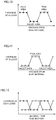
- Graph A which is obtained by putting plots of A 1 to A 10 layers on a coordinate system and by connecting the plots with a straight line, the coordinate system having a vertical axis representing the thickness of each layer and having a horizontal axis representing the distance of each layer from the base material, shows a wavy pattern where a peak area and a valley area are alternately repeated as shown in Fig. 2 .
- the distance of each layer from the base material is defined as the distance between the intermediate position of the base material and the intermediate position of each layer in the thickness direction.
- peak areas in graph A refer to areas where the thickness continuously increases from an intermediate point to a local maximum point and then continuously decreases to the next intermediate point
- valley areas refer to areas where the thickness continuously decreases from an intermediate point to a local minimum point and then continuously increases to the next intermediate point.
- the intermediate point refers to a point having a value that is intermediate between the value of the local maximum point and the value of the local minimum point adjacent to the local maximum point.
- the drawing shows a case where three intermediate points have the same value, i.e., the intermediate point (2.5 nm) between 4 nm (local maximum point) and 1 nm (local minimum point).
- the intermediate points may have different values. The same applies to graph B described later.
- Graph B which is obtained by putting plots of B 1 to B 10 layers on a coordinate system and by connecting the plots with a straight line, the coordinate system having a vertical axis representing the thickness of each layer and having a horizontal axis representing the distance of each layer from the base material, shows a wavy pattern where a peak area and a valley area are alternately repeated as shown in Fig. 3 .
- B 1 to B 3 layers and B 7 to B 9 layers are the B layers constituting valley areas
- four layers, B 4 to B 6 layers and B 10 layer are the B layers constituting peak areas.
- peak areas in graph B refer to areas where the thickness continuously increases from an intermediate point to a local maximum point and then continuously decreases to the next intermediate point
- valley areas refer to areas where the thickness continuously decreases from an intermediate point to a local minimum point and then continuously increases to the next intermediate point.
- a layers can also be described as having an area where the thickness continuously increases and an area where the thickness continuously decreases from the base material side to the surface side, the areas being alternately repeated.
- B layers can also be described as having an area where the thickness continuously increases and an area where the thickness continuously decreases from the base material side to the surface side, the areas being alternately repeated.
- Fig. 4 is a graph obtained by superimposing Fig. 2 and Fig. 3 on each other.
- Fig. 4 shows that, in the first super-multilayer-structure layer, in the areas in which the thickness of A layer continuously increases from the base material side to the surface side, the thickness of B layer continuously decreases from the base material side to the surface side, whereas in the areas in which the thickness of A layer continuously decreases from the base material side to the surface side, the thickness of B layer continuously increases from the base material side to the surface side. Therefore, it can be said that a change in thickness of A layer and a change in thickness of B layer are relative to each other.
- the first super-multilayer-structure layer can then be defined as:
- coating 2 includes the first super-multilayer-structure layer that satisfies the above (1) to (6) can be checked as follows. First, a sample prepared in a way similar to the above-described way using a scanning transmission electron microscopy (STEM) is observed with a magnification of 200, 000 times or more and thus a high-angle annular dark-field (HAADF) image is obtained.
- STEM scanning transmission electron microscopy
- HAADF high-angle annular dark-field
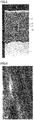
- Fig. 5 is a photograph as a substitute for a drawing that has captured a microscope image of a super-multilayer-structure layer.
- Fig. 6 is a photograph as a substitute for a drawing showing the part enclosed by a broken line in Fig. 5 in an enlarged view.
- repetition of X areas and Y areas of the super-multilayer-structure layer is observed.
- Fig. 6 a multilayer structure within each X area and a multilayer structure within each Y area are further observed.
- the super-multilayer-structure layer of Fig. 5 includes A layers composed of AlCrN and B layers composed of AlTiSiN.
- a layers having a small formula weight (the total of the atomic weights of the constituent elements) are observed as a dark hue (black), whereas B layers having a large formula weight are observed as a light hue (gray or white).
- B layers having a large formula weight are observed as a light hue (gray or white).
- X areas containing relatively thick A layers are observed as a relatively dark hue
- Y areas containing relatively thin A layers are observed as a relatively light hue.
- each of X areas and Y areas has a structure where a plurality of dark-colored areas (A layers) and a plurality of light-colored areas (B layers) are laminated as shown in Fig. 6 .
- an intensity profile (Z contrast) in the thickness direction (the direction indicated by the arrow in Fig. 6 ) of the super-multilayer-structure layer is obtained.
- a graph is created on a coordinate system having a vertical axis representing the strength and having a horizontal axis representing the distance from a measurement starting point.
- the strength of the Z contrast is proportional to the square of the atomic weight. Accordingly, A layers composed of AlCrN and B layers composed of AlTiSiN can be distinguished from each other based on the contrast intensity profile.
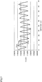
- Fig. 7 is a graph showing a contrast intensity profile in the direction of the arrow in the microscope image (HAADF image) shown in Fig. 6 .
- a layers composed of AlCrN and B layers composed of AlTiSiN being compared with each other, A layers contain the atom having the highest atomic weight (Cr). Therefore, A layers show a higher strength than B layers.
- the areas presenting a convex shape in Fig. 7 can be regarded as A layers
- the areas presenting a concave shape in Fig. 7 can be regarded as B layers.
- the intermediate point P mid between the local maximum point P max in one convex area and the local minimum point P min in one concave area adjacent to the convex area is determined as a boundary between the convex area and the concave area (i.e., the boundary between an A layer and a B layer). The same applies to other boundaries.
- the boundaries between A layers and B layers are thus determined, and the thickness of each A layer and the thickness of each B layer can be accordingly determined.
- the determination of the thickness of each layer can determine X areas and Y areas that are distinguished from each other by the thickness of each layer.
- the fact that A layers and B layers are alternately laminated and that X areas and Y areas are alternately repeated can also be checked by the light and shade of the HAADF image as described above. Further, based on the result of the thickness of each layer, graph A and graph B can be created.
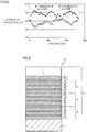
- Fig. 8 is a graphic plot on a coordinate system having a vertical axis representing the thickness of each layer and having a horizontal axis representing the distance from a measurement starting point for A layers and B layers included in the super-multilayer-structure layer, based on the intensity profile of Fig. 7 .
- Graph A is obtained by connecting the hollow-square plots of Fig. 8 with a straight line
- graph B is obtained by connecting the black-rhombus plots of Fig. 8 with a straight line.
- the graph of Fig. 8 shows that, in the super-multilayer-structure layer of Fig. 5 , A layers have a thickness of about 2 to 5 nm, B layers have a thickness of about 4 to 7 nm, and B layers tend to be larger than A layers in thickness as a whole.
- composition of each layer can be checked by analyzing the above HAADF image using EDX equipment incidental to a TEM. At this time, the spot diameter is set to 1 nm, and the algebraic mean value of compositional ratios obtained at five randomly-selected points in each layer is defined as a composition.
- the first super-multilayer-structure layer described above in detail can exhibit both characteristics based on A layers and characteristics based on B layers. Further, the first super-multilayer-structure layer can also exhibit characteristics based on X areas and characteristics based on Y areas. Consequently, coating 2 can exhibit many and various characteristics compared to a conventional one.
- the first super-multilayer-structure layer is characterized in that the thickness of A layer repeats continuous increase and decrease from the base material side to the surface side, and in that the thickness of B layer repeats continuous increase and decrease from the base material side to the surface side.
- a super-multilayer-structure layer having such a construction prevents interlayer peeling more sufficiently.
- a conceivable reason is that a gentle change of each layer thickness in the thickness direction of the super-multilayer-structure layer can maintain a small stress difference between the layers. Therefore, the first super-multilayer-structure layer has a remarkably long tool life.
- a second super-multilayer-structure layer which is another example super-multilayer-structure layer according to this embodiment, will be specifically described.
- the second super-multilayer-structure layer satisfies the above (1) to (6).
- the second super-multilayer-structure layer is different from the first super-multilayer-structure layer in the shape of each "peak area” and “valley area” in graph A, and in the shape of each "peak area” and “valley area” in graph B.
- the A layer located closest to the base material is referred to as A 1 layer, and the A layers are referred to as A 1 layer, A 2 layer, A 3 layer, ... A 10 layer in this order from the base material side to the surface side.
- the B layer located closest to the base material is referred to as B 1 layer, and the B layers are referred to as B 1 layer, B 2 layer, B 3 layer, ... B 10 layer in this order from the base material side to the surface side.
- a 1 layer to A 10 layer have thicknesses of 4 nm, 4 nm, 4 nm, 1 nm, 1 nm, 1 nm, 4 nm, 4 nm, and 1 nm, respectively, and that B 1 layer to B 10 layer have thicknesses of 1 nm, 1 nm, 1 nm, 4 nm, 4 nm, 4 nm, 1 nm, 1 nm, and 4 nm, respectively.
- Fig. 9 shows ten A layers and ten B layers, it is needless to say that, on B 10 layer, the top layer, there may be a laminated structure where A layers and B layers are laminated in this order (this is represented by dots in Fig. 9 ).
- the second super-multilayer-structure layer includes A layers (A 1 to A 3 layers and A 7 to A 9 layers) having a thickness of 4 nm, and A layers (A 4 to A 6 layers and A 10 layer) having a thickness of 1 nm. Further, the second super-multilayer-structure layer includes B layers (B 1 to B 3 layers and B 7 to B 9 layers) having a thickness of 1 nm, and B layers (B 4 to B 6 layers and B 10 layer) having a thickness of 4 nm.
- an area where A 4 to A 5 layers having a thickness of 1 nm and B 4 to B 6 layers having a thickness of 4 nm are alternately laminated as shown in Fig. 9 is a Y area.
- the thickness of each of A 1 to A 3 layers and A 7 to A 9 layers constituting X areas is 4 nm, and the thickness of each of A 4 to A 6 layers constituting a Y area is 1 nm.
- the thickness of each of B 1 to B 3 layers and B 7 to B 9 layers constituting X areas is 1 nm, and the thickness of each of B 4 to B 6 layers constituting a Y area is 4 nm.
- the second super-multilayer-structure layer has a construction in which an X area and a Y area are alternately repeated from the base material side to the surface side, the X area being an area where A layers having thickness A X and B layers having thickness B X are alternately laminated, the Y area being an area where A layers having thickness A Y and B layers having thickness B Y are alternately laminated. Further, thickness A X (4 nm) of the A layers constituting X areas is larger than thickness A Y (1 nm) of the A layers constituting Y areas, and thickness B X (1 nm) of the B layers constituting X areas is smaller than thickness B Y (4 nm) of the B layers constituting Y areas.
- Graph A created for A 1 to A 10 layers shows a wavy pattern where a peak area and a valley area are alternately repeated as shown in Fig. 10 .
- graph B created for B 1 to B 10 layers shows a wavy pattern where a peak area and a valley area are alternately repeated as shown in Fig. 11.
- Fig. 12 is a graph obtained by superimposing Fig. 10 and Fig. 11 on each other.
- a "peak area” refers to an area where the thickness increases from an intermediate point to a local maximum point and then decreases to the next intermediate point
- a "valley area” refers to an area where the thickness decreases from an intermediate point to a local minimum point and then increases to the next intermediate point.
- a "peak area” and a "valley area” in each graph are each constituted of layers having the same thickness. That is, graph A and graph B in the second embodiment is characterized by having a rectangular waveform, rather than having a sinusoidal waveform having local maximum points and local minimum points as in the first embodiment.
- coating 2 can also exhibit many and various characteristics compared to a conventional one and allows for a remarkably long tool life for the same reasons described above.
- the first super-multilayer-structure layer and the second super-multilayer-structure layer have been described above as examples of a super-multilayer-structure layer according to this embodiment. More preferred embodiments of a super-multilayer-structure layer according to this embodiment are enumerated below.
- an XY area composed of an X area and one Y area adjacent to the X area may have a thickness of, for example, 30 to 2500 nm.
- the thickness of the XY area is preferably less than or equal to 300 nm.
- an XY area composed of an X area and one Y area adjacent to the X area may include, for example, 3 to 15 A layers and 3 to 15 B layers.
- the XY area preferably includes 4 to 10 A layers and 4 to 10 B layers.
- the presence of four or more layers allows for a further gentle change in thickness of each layer in each area.
- the presence of more than ten layers, though making the change in thickness of each layer gentler makes it difficult to control the structure of the super-multilayer-structure layer and may consequently cause uneven characteristics. Therefore, the XY area including 4 to 10 A layers and 4 to 10 B layers can more reliably prevent the interlayer peeling in the super-multilayer-structure layer, thus allowing tool 10 to have a further longer life.
- each of A layers and B layers may have a thickness of, for example, 0.5 to 100 nm.
- each of A layers and B layers preferably has a thickness of 0.5 to 30 nm.
- the super-multilayer-structure layer composed of A layers and B layers having such a thickness can more reliably prevent the interlayer peeling.
- the super-multilayer-structure layer preferably has a thickness of 1 to 20 ⁇ m.
- a super-multilayer-structure layer having a thickness of less than 1 ⁇ m may not be able to sufficiently exhibit the effects of the super-multilayer-structure layer.
- a super-multilayer-structure layer having a thickness of more than 20 ⁇ m may cause peeling of the super-multilayer-structure layer due to a great pressure applied during cutting.
- each A layer is preferably a compound layer containing Al, Cr, and N
- each B layer is preferably a compound layer containing Al, Ti, Si, and N.
- Such A layers tend to have good oxidation resistance in particular, and such B layers tend to have high hardness in particular. Oxidation resistance and hardness are characteristics closely related to the life of a cutting tool.
- a coating including a super-multilayer-structure layer composed of such A layers and B layers will allow tool 10 to have a particularly long tool life.
- the super-multilayer-structure layer preferably has a hardness H of 35 GPa or more and the ratio H / E of hardness H to Young's modulus E is preferably 0.5 or more.
- Such a super-multilayer-structure layer has better abrasion resistance as well as breaking strength. Accordingly, it can exhibit particularly high performance during cutting of a difficult-to-cut material, such as a heat-resistant alloy.
- Hardness H and Young's modulus E of the super-multilayer-structure layer can be obtained based on the nanoindentation technique in ISO 14577-1:2015. Specifically, hardness H and Young's modulus E are obtained by indenting an indenter with a load controlled so that the indentation depth in a surface of the super-multilayer-structure layer will be 0.2 ⁇ m. Examples of ultra-micro indentation hardness testers to which the nanoindentation technique is applicable include "ENT-1100a" manufactured by ELIONIX Inc. With the presence of another layer (e.g. surface layer) on the super-multilayer-structure layer, the super-multilayer-structure layer is exposed through, for example, calotest and diagonal wrapping.
- another layer e.g. surface layer
- the upper limit value of hardness H of the super-multilayer-structure layer is not particularly limited, it is preferably less than or equal to 45 GPa from a viewpoint of improvement in resistance to chipping. Further, ratio H/E is preferably less than or equal to 0.12 from a viewpoint of consistency with the elastic deformation characteristics of the base material.
- a surface-coated cutting tool including a coating containing the above-described super-multilayer-structure layer can be manufactured by the following method.
- the manufacturing method includes a step of preparing at least a base material and a step of forming a coating.
- a base material is prepared.
- a base material composed of a cemented carbide may be prepared by common powder metallurgy.
- a WC powder and a Co powder for example, are mixed by a ball mill to produce a mixture powder.
- the mixture powder is dried and is then formed into a predetermined shape to produce a compact.
- the compact is then sintered to produce a WC-Co based cemented carbide (sintered body).
- the sintered body is then subjected to predetermined cutting edge machining, such as honing, as needed to prepare a base material composed of a WC-Co based cemented carbide.
- a coating is formed by a PVD method.
- PVD methods include arc ion plating (AIP), balanced magnetron sputtering, and unbalanced magnetron sputtering. From a viewpoint of ease of manufacturability of a super-multilayer-structure layer, the use of the AIP method is preferred.
- a deposition apparatus 100 shown in Fig. 13 and Fig. 14 includes a chamber 20, a gas inlet 21 for introducing a source gas into chamber 20, and a gas outlet 22 for discharging the source gas to the outside.
- Chamber 20 is connected to a vacuum pump (not shown) and is configured to adjust the pressure in chamber 20 through gas outlet 22.
- a rotary table 23 is provided.
- a base material holder 24 for holding base material 1 is attached to rotary table 23.
- Base material holder 24 is electrically connected to the negative electrode of a bias power supply 25.
- the positive electrode of bias power supply 25 is grounded and is also electrically connected to chamber 20.
- arc evaporation sources (targets 25a, 25b) are attached to the side walls of chamber 20, the arc evaporation sources being metal raw material of each layer constituting a coating.
- the arc evaporation sources are connected to the respective negative electrodes of DC power supplies 26a, 26b (which are variable power supplies).
- the positive electrodes of DC power supplies 26a, 26b are grounded.
- layers other than a super-multilayer-structure layer are formed in the following way.
- base material 1 is attached to base material holder 24 in deposition apparatus 100.
- the pressure in chamber 20 is reduced by a vacuum pump (e.g. about 1.0 x 10 -4 Pa).
- base material 1 is heated by a heater (not shown) provided in deposition apparatus 100 while rotating rotary table 23 at a constant speed.
- a bias voltage is applied to base material 1 while introducing a reactive gas through gas inlet 21, the reactive gas containing a nonmetallic element (C, N, B, or O) among the atoms that constitute the layer. Further, an identical and constant arc current is supplied to targets 25a, 25b.
- Targets 25a, 25b are a reactive gas containing a metallic element among the atoms that constitute the layer.
- a bias voltage applied to base material 1 may be made smaller during deposition of the surface layer than during deposition of the super-multilayer-structure layer, for example.
- layers other than a super-multilayer-structure layer such as a primary layer and a surface layer, are formed. It is preferred that an ion bombardment be performed on a surface of the base material prior to formation of a coating. This is because the ion bombardment can clean the base material surface and can enhance the homogeneity of a coating to be formed on the base material surface.
- the AIP method allows this process to be easily performed.
- a method of manufacturing a super-multilayer-structure layer of a coating is significantly different from the above method in that an arc current to be supplied to targets 25a, 25b is changed.
- a reactive gas a gas containing C and/or N is used.
- target 25a is a metal raw material containing a metallic element that constitutes A layers and target 25b is a metal raw material containing a metallic element that constitutes B layers
- a current to be supplied to target 25a is changed over time to correspond a change in thickness of A layer
- a current to be supplied to target 25b is changed over time to correspond a change in thickness of B layer.
- An A layer deposited with a high current supplied to target 25a is thick, whereas an A layer deposited with a low current supplied to target 25a is thin.
- a B layer deposited with a high current supplied to target 25b is thick, whereas a B layer deposited with a low current supplied to target 25b is thin.
- the magnitude of current to be supplied to target 25a is changed to correspond to the graph shown in Fig. 2
- the magnitude of current to be supplied to target 25b is changed to correspond to the graph shown in Fig. 3
- the magnitude of current to be supplied to target 25a is changed to correspond to the graph shown in Fig. 10
- the magnitude of current to be supplied to target 25b is changed to correspond to the graph shown in Fig. 11 .
- each layer that constitutes a super-multilayer-structure layer can be controlled by controlling the magnitude of current to be supplied to each target.
- the overall thickness of a layer to be formed can be increased by slowing down the speed of rotation of the rotary table.
- the number of times each layer is deposited and the thickness of the super-multilayer-structure layer can be controlled by adjusting the processing time. Further, the number of A layers and B layers included in each XY area can be controlled by adjusting the current supplying time. In this way, the super-multilayer-structure layer is formed.
- deposition apparatus 100 having a monoaxial rotation mechanism.
- the thickness of each layer that constitutes the super-multilayer-structure layer can be controlled by adjusting each rotational period of the triaxial rotation mechanism.
- the present invention will be described in more detail below with Examples. The present invention, however, is not limited to the Examples.
- the surface-coated cutting tools of No. 1 to No. 9 each include the above-described second super-multilayer-structure layer.
- No. 10 to No. 18 are comparative examples.
- the surface-coated cutting tools of No. 19 to No. 50 each include the above-described first super-multilayer-structure layer.
- each layer constituting the super-multilayer-structure layer was obtained from the intensity profile of Z contrast obtained from a HAADF image. Further, graph A and graph B were created based on the thickness of each layer, and the information (such as the number of A layers and B layers constituting each X area and each Y area, and the thickness of each XY area) obtained from each graph was checked. The composition of each layer was checked by analyzing the HAADF image using EDX equipment incidental to a TEM as in the above-described method.
- a drill made of cemented carbide (JIS K10), shape: MDW0800HGS5) having an external diameter of 8 mm was prepared.
- the base material was then placed in chamber 20 of deposition apparatus 100 having a monoaxial rotation mechanism shown in Fig. 13 and chamber 20 was vacuumed. After that, the base material was heated to 500°C while rotary table 23 was rotated at 3 rpm.
- Ar gas was then introduced into vacuum chamber 20 at 1 Pa, a tungsten filament was electrically discharged to generate Ar ion, and a bias voltage of -500 V was applied to the base material.
- an ion bombardment of the tool base material using Ar ion was performed.
- No. 1 super-multilayer-structure layer was deposited on a surface of the base material after etching.
- the features of No. 1 super-multilayer-structure layer are shown in Table 1.
- Table 1 A layer B layer XY area Super-multilayer-structure layer Composition Thickness A X (nm) Thickness A Y (nm) Composition Thickness B X (nm) Thickness B Y (nm) Thickness (nm) Number of A layers Number of B layers Thickness ( ⁇ m) No.1 Al 0.7 Cr 0.3 N 48 36 Ti 0.5 Al 0.5 N 57 71 1590 15 15 15 4.8 No.2 Al 0.67 Ti 0.33 N 63 49 Ti 0.5 Al 0.5 N 53 69 1760 15 15 5.3 No.3 Ti 0.5 Al 0.5 N 70 53 Ti 0.9 Si 0.1 N 55 68 1850 15 15 5.5 No.4 Ti 0.5 Al 0.5 N 73 58 Ti 0.9 Nb 0.1 N 58 75 1980 15 15 5.9 No.5 Ti 0.5
- No. 1 super-multilayer-structure layer had a construction in which an X area and a Y area were alternately repeated from the base material side to the surface side, the X area being an area where A layers having a thickness of 48 nm (thickness A X ) and B layers having a thickness of 57 nm (thickness B X ) were alternately laminated, the Y area being an area where A layers having a thickness of 36 nm (thickness A Y ) and B layers having a thickness of 71 nm (thickness B Y ) were alternately laminated.
- the composition of A layers was Al 0.7 Cr 0.3 N
- the composition of B layers was Ti 0.5 Al 0.5 N.
- each XY area was 1590 nm, the number of A layers included in each XY area was 15, and the number of B layers included in each XY area was 15.
- the deposition conditions for this super-multilayer-structure layer are shown below.
- Target A Al (70 at%) and Cr (30 at%)
- Target B Ti (50 at%) and Al (50 at%)
- Introduced gas N 2
- Deposition pressure 6.0 Pa
- Current supply to target A Repeat step of supplying 150 A for 60 s (A X step) and subsequent step of supplying 150 A for 45 s (A Y step)
- Current supply to target B Repeat step of supplying 150 A for 65 s (B X step) and subsequent step of supplying 150 A for 80 s (B Y step)
- Substrate bias voltage 50 V
- Control was performed so that, when the arc current supply to target A was A X step, the arc current supply to target B was B X step; and so that, when the arc current supply to target A was A Y step, the arc current supply to target B was B Y step.
- a layers having thickness A X were formed by A X step
- a layers having thickness A Y were formed by A Y step
- B layers having thickness B X were formed by B X step
- B layers having thickness By were formed by By step.
- No. 2 to No. 9 surface-coated cutting tools were manufactured in the same way as No. 1 except that the constructions of the super-multilayer-structure layers were changed as shown in Table 1 by changing the deposition conditions of the super-multilayer-structure layers.
- thickness A X of A layers to constitute X areas, thickness A Y of A layers to constitute Y areas, thickness B X of B layers to constitute X areas, and thickness B Y of B layers to constitute Y areas were adjusted by increasing and decreasing the magnitude of the arc current in each of A X step, A Y step, B X step, and By step. Note that a greater arc current makes each layer thicker, and that a smaller arc current makes each layer thinner.
- the number of A layers to constitute each X area, the number of A layers to constitute each Y area, the number of B layers to constitute each X area, and the number of B layers to constitute each Y area were adjusted by increasing and decreasing the period of time of each of A X step, A Y step, B X step, and B Y step. Note that a longer supply time makes the number of layers larger, and that a shorter supply time makes the number of layers smaller.
- target A and target B had the same composition, and target A and target B were continuously supplied with the same-magnitude arc current (150 A).
- target A composed of metallic element to constitute each A layer and target B composed of metallic element to constitute each B layer were used, and target A and target B were continuously supplied with the same-magnitude arc current (150 A).
- Drilling tests were conducted with No. 1 to No. 18 surface-coated cutting tools under the following conditions. Each time 100 holes were newly drilled, the accuracy of dimension of the last-drilled hole was checked, and if the accuracy of dimension was outside of a prescribed range, the life of the surface-coated cutting tool was determined to be exhausted and the test was stopped. Table 3 shows the number of holes that each surface-coated cutting tool was able to make. The larger number of holes shows that the tool was able to drill a larger number of holes with prescribed accuracy of dimension and that the tool life was longer. Note that the prescribed range was 8.000 to 8.036 mm. Workpiece : S50C (HB200) Cutting speed : 70 m/min Feed rate : 0.25 mm/rev Hole depth : 24 mm blind-hole Cutting oil : With cutting oil (externally supplied oil)
- Drilling tests were conducted with No. 1 to No. 18 surface-coated cutting tools under the following conditions. Each time 100 holes were newly drilled, the accuracy of dimension of the last-drilled hole was checked, and if the accuracy of dimension was outside of a prescribed range, the life of the surface-coated cutting tool was determined to be exhausted and the test was stopped. Table 3 shows the number of holes that each surface-coated cutting tool was able to make. The larger number of holes shows that the tool was able to drill a larger number of holes with prescribed accuracy of dimension and that the tool life was longer. Note that the prescribed range was 8.000 to 8.036 mm.
- No. 19 to No. 50 surface-coated cutting tools were manufactured in the same way as No. 1 except that the constructions of the super-multilayer-structure layers were changed as shown in Table 4 by changing the deposition conditions of the super-multilayer-structure layers.
- Target A Al (70 at%) and Cr (30 at%)
- Target B Al (58 at%), Ti (38 at%), and Si (4 at%)
- Introduced gas N 2 Deposition pressure : 6.0 Pa
- Current supply to target A Repeat step of increasing from 100 A to 200 A at a speed of 20 A/min and then decreasing to 100 A at the same speed (A X step), and step of decreasing from 200 A to 100 A at a speed of 20 A/min and then increasing to 200 A at the same speed (A Y step)
- Control was performed so that, when the arc current supply to target A was A X step, the arc current supply to target B was B X step; and so that, when the arc current supply to target A was A Y step, the arc current supply to target B was B Y step.
- a layers having thickness A X were formed by A X step
- a layers having thickness A Y were formed by A Y step
- B layers having thickness B X were formed by B X step
- B layers having thickness By were formed by By step.
- the manufacture conditions of No. 19 super-multilayer-structure layer are significantly different from those of No. 1 super-multilayer-structure layer in that each arc current to be supplied to target A and target B repeats a continuous increase and a continuous decrease. Accordingly, in No. 19 super-multilayer-structure layer, the thickness of A layer and the thickness of B layer continuously increase and decrease from the base material side to the surface side. In addition, in the area where the thickness of A layer continuously increases, the thickness of B layer continuously decreases, whereas in the area where the thickness of A layer continuously decreases, the thickness of B layer continuously increases.
- thickness A X , thickness A Y , thickness B X , and thickness B Y each have a plurality of thicknesses.
- Table 4 shows only the maximum value of thickness A X (i.e., the value of a local maximum point of graph A), the minimum value of thickness A Y (i.e., the value of a local minimum point of graph A), the minimum value of thickness B X (i.e., the value of a local minimum point of graph B), and the maximum value of thickness B Y (i.e., the value of a local maximum point of graph B).
- No. 20 to No. 50 surface-coated cutting tools were manufactured in the same way as No. 9 except that the constructions of the super-multilayer-structure layers were changed as shown in Table 4 and Table 5 by changing the deposition conditions of the super-multilayer-structure layers.
- the maximum value of thickness A X of A layers to constitute each X area, the minimum value of thickness A Y of A layers to constitute each Y area, the maximum value of thickness B X of B layers to constitute each X area, and the minimum value of thickness B Y of B layers to constitute each Y area were adjusted by increasing and decreasing the maximum value and the minimum value of the magnitude of the arc current in each of A X step, A Y step, B X step, and B Y step.
- the number of A layers to constitute each X area, the number of A layers to constitute each Y area, the number of B layers to constitute each X area, and the number of B layers to constitute each Y area were adjusted by increasing and decreasing the period of time of each of A X step, A Y step, B X step, and B Y step.
- a layer B layer XY area Super-multilayer-structure layer Composition Maximum value of thickness A X (nm) Minimum value of thickness A Y (nm) Composition Minimum value of thickness B X (nm) Maximum value of thickness By (nm) Thickness (nm) Number of A layers Number of B layers Thickness ( ⁇ m) No.19 76 35 Al 0.58 Ti 0.38 Si 0.04 N 66 91 2010 15 15 4.0 No.20 70 31 Ti 0.48 Al 0.48 Si 0.04 N 59 83 1820 15 15 3.6 No.21 72 33 Ti 0.58 Al 0.38 Si 0.04 N 54 76 1760 15 15 3.5 No.22 55 35 Al 0.58 Ti 0.38 Si 0.04 N 36 65 290 3 3 4.1 No.23 40 31 Al 0.58 Ti 0.38 Si 0.04 N 31 41 210 3 3 4.2 No.24 39 31 Ti 0.48 Al 0.48 Si 0.04 N 33 48 230 3 3 4.1 No.25 Al 0.7 Cr 0.3 N 42 33 Al 0.58 Ti 0.38 Si 0.04 N 31 45
- Test 1 and test 2 were conducted in a similar way to Examination 1. The results are shown in Table 6.
- Test 1 Test 2 Number of holes Number of holes No.19 5500 8100 No.20 5600 7800 No.21 5800 7700 No.22 6000 8600 No.23 6200 8800 No.24 6200 8600 No.25 6300 8400 No.26 7900 9800 No.27 8000 10400 No.28 8100 11200 No.29 8200 11200 No.30 8400 11400 No.31 8600 11600 No.32 8800 11800 No.33 9000 12000 No.34 8700 11700 No.35 8500 11500 No.36 7200 12500 No.37 7000 12800 No.38 7400 13000 No.39 8000 13300 No.40 8000 13500 No.41 7800 13300 No.42 7600 13000 No.43 7400 12800 No.44 7200 12800 No.45 6600 9200 No.46 6600 9200 No.47 6600 9200 No.48 6800 9500 No.49 6900 9600 No.
- each A layer was a compound layer containing Al, Cr, and N
- each B layer was a compound layer containing Al, Ti, Si, and N.
- a super-multilayer-structure layer including A layers and B layers having a composition other than such a composition can also provide a sufficiently long tool life.
- 1 base material; 2: coating; 10: surface-coated cutting tool; 20: chamber; 21: gas inlet; 22: gas outlet; 23: rotary table; 24: base material holder; 25a, 25b: target; 26a, 26b: arc evaporation source; 100: deposition apparatus
Landscapes
- Chemical & Material Sciences (AREA)
- Engineering & Computer Science (AREA)
- Mechanical Engineering (AREA)
- Organic Chemistry (AREA)
- Materials Engineering (AREA)
- Metallurgy (AREA)
- Chemical Kinetics & Catalysis (AREA)
- Inorganic Chemistry (AREA)
- Ceramic Engineering (AREA)
- Drilling Tools (AREA)
- Cutting Tools, Boring Holders, And Turrets (AREA)
- Milling, Broaching, Filing, Reaming, And Others (AREA)
- Physical Vapour Deposition (AREA)
Abstract
Description
- The present invention relates to a surface-coated cutting tool. The present application claims a priority based on Japanese Patent Application No.
2016-231723 filed on November 29, 2016 - As a cutting tool, there is known a surface-coated cutting tool which includes a base material having a coating on its surface and thereby exhibits characteristics of the base material and characteristics of the coating. For example, Japanese Patent Laying-Open No.
2013-176837 - In such a layer having a multilayer structure (multilayer-structure layer) in which two or more types of layers are repeatedly laminated, the layers are usually designed to have the same thickness from a viewpoint of homogeneity in characteristics, for example. However, there has also been another technique in which to provide a multilayer-structure layer including layers with varied thicknesses to provide distinctive characteristics that could not be exhibited by the same-thickness layers.
- For example,
WO 2006/070730 (PTD 2) discloses an alternating layer obtained by alternately laminating A layers excellent in oxidation resistance and B layers providing good adhesion to a coating, where the ratio λa / λb of the A layer thickness λa to the B layer thickness λb continuously increases as the distance from a base material increases.PTD 2 discloses that the coating containing such an alternating layer is excellent in oxidation resistance, provides good adhesion to the coating, and can prevent crack extension, thus allowing a surface-coated cutting tool to have a long life. - Further, Japanese Patent Laying-Open No.
2008-162009 -
- PTD 1: Japanese Patent Laying-Open No.
2013-176837 - PTD 2:
WO 2006/070730 - PTD 3: Japanese Patent Laying-Open No.
2008-162009 - A surface-coated cutting tool according to one aspect of the present disclosure is a surface-coated cutting tool including a base material and a coating covering a surface of the base material. The coating includes a super-multilayer-structure layer where A layers and B layers different from the A layers in composition are alternately laminated from the base material side to the surface side. The super-multilayer-structure layer has a construction in which an X area and a Y area are alternately repeated from the base material side to the surface side, the X area being an area where A layers having a thickness AX and B layers having a thickness BX are alternately laminated, the Y area being an area where A layers having a thickness AY and B layers having a thickness BY are alternately laminated. The thickness AX of the A layers is larger than the thickness AY of the A layers, and the thickness BX of the B layers is smaller than the thickness BY of the B layers. Each of the A layers and the B layers has a composition comprising one or more elements selected from a group consisting of Ti, Al, Cr, Si, Ta, Nb, and W, and one or more elements selected from a group consisting of C and N.
-
-
Fig. 1 is a cross-sectional view schematically showing a construction of a coating included in a surface-coated cutting tool in one embodiment. -
Fig. 2 is a graphic plot on a coordinate system having a vertical axis representing the thickness of each layer and having a horizontal axis representing the distance of each layer from a base material for A layers included in the super-multilayer-structure layer ofFig. 1 . -
Fig. 3 is a graphic plot on a coordinate system having a vertical axis representing the thickness of each layer and having a horizontal axis representing the distance of each layer from the base material for B layers included in the super-multilayer-structure layer ofFig. 1 . -
Fig. 4 is a graphic plot on a coordinate system having a vertical axis representing the thickness of each layer and having a horizontal axis representing the distance of each layer from the base material for A layers and B layers included in the super-multilayer-structure layer ofFig. 1 . -
Fig. 5 is a photograph as a substitute for a drawing that has captured a microscope image of a super-multilayer-structure layer. -
Fig. 6 is a photograph as a substitute for a drawing showing the part enclosed by a broken line inFig. 5 in an enlarged view. -
Fig. 7 is a graph showing a contrast intensity profile in the direction of the arrow in the microscope image shown inFig. 6 . -
Fig. 8 is a graphic plot on a coordinate system having a vertical axis representing the thickness of each layer and having a horizontal axis representing the distance from a measurement starting point for A layers and B layers included in the super-multilayer-structure layer, based on the intensity profile ofFig. 7 . -
Fig. 9 is a cross-sectional view schematically showing another construction of a coating included in a surface-coated cutting tool in one embodiment. -
Fig. 10 is a graphic plot on a coordinate system having a vertical axis representing the thickness of each layer and having a horizontal axis representing the distance of each layer from a base material for A layers included in the super-multilayer-structure layer ofFig. 9 . -
Fig. 11 is a graphic plot on a coordinate system having a vertical axis representing the thickness of each layer and having a horizontal axis representing the distance of each layer from the base material for B layers included in the super-multilayer-structure layer ofFig. 9 . -
Fig. 12 is a graphic plot on a coordinate system having a vertical axis representing the thickness of each layer and having a horizontal axis representing the distance of each layer from the base material for A layers and B layers included in the super-multilayer-structure layer ofFig. 9 . -
Fig. 13 is a schematic side perspective view showing one example configuration of a deposition apparatus that can be used for an AIP method. -
Fig. 14 is a schematic plan perspective view of the deposition apparatus ofFig. 13 . - A surface-coated cutting tool tends to have different damage morphologies depending on the portion. For example, in grinding with a throw away tip, a rake face and a flank face are significantly different from each other in damage morphology. In drilling with a drill, a groove portion near the rotating shaft of the drill and a peripheral cutting-edge portion remote from the rotating shaft are significantly different from each other in damage morphology.
- Although conventional techniques can reduce a damage on a specific portion of a surface-coated cutting tool, it is actually difficult to sufficiently reduce damages having different morphologies on a plurality of portions. A surface-coated cutting tool will end its life when the working accuracy of a workpiece drops to less than or equal to a threshold value. Accordingly, if each of damages having different morphologies contained in one tool cannot be sufficiently reduced, then a working accuracy for a workpiece will be decreased and the tool life will be shortened. In other words, there is yet room for an increase in life of a surface-coated cutting tool.
- An object of the present disclosure is to provide a surface-coated cutting tool having a long tool life.
- According to the present disclosure, a surface-coated cutting tool having a long tool life can be provided.
- First, embodiments of the present invention are enumerated. In this description, an expression in the form of "M to N" represents the upper and lower limits of a range (i.e., M to N both inclusive). M with no unit and only N with a unit means that M and N have the same unit.
- (1) A surface-coated cutting tool according to one aspect of the present disclosure includes a base material, and a coating covering a surface of the base material. The coating includes a super-multilayer-structure layer where A layers and B layers different from the A layers in composition are alternately laminated from the base material side to the surface side. The super-multilayer-structure layer has a construction in which an X area and a Y area are alternately repeated from the base material side to the surface side, the X area being an area where A layers having a thickness AX and B layers having a thickness BX are alternately laminated, the Y area being an area where A layers having a thickness AY and B layers having a thickness By are alternately laminated. The thickness AX of the A layers is larger than the thickness Ay of the A layers, and the thickness BX of the B layers is smaller than the thickness BY of the B layers. Each of the A layers and the B layers has a composition comprising one or more elements selected from a group consisting of Ti, Al, Cr, Si, Ta, Nb, and W, and one or more elements selected from a group consisting of C and N.
The coating included in the surface-coated cutting tool has a super-multilayer-structure layer where A layers and B layers are alternately laminated. Accordingly, both characteristics based on the A layers and characteristics based on the B layers can be exhibited. Further, the super-multilayer-structure layer has a construction in which an X area and a Y area are alternately repeated, the X area being an area where A layers having thickness AX and B layers having thickness BX are alternately laminated, the Y area being an area where A layers having thickness AY and B layers having thickness By are alternately laminated, where AX>AY and BX<BY are satisfied. Therefore, characteristics based on the X area and characteristics based on the Y area can also be exhibited.
Thus, the coating can exhibit many and various characteristics compared to a conventional one. Accordingly, if a specific damage easily occurs at one portion of a surface-coated cutting tool and another specific damage easily occurs at another portion, then the damages to the both portions can be appropriately reduced. Therefore, it is possible for the surface-coated cutting tool to have a long tool life. - (2) In the surface-coated cutting tool, on a coordinate system having a vertical axis representing the thickness and having a horizontal axis representing the distance from the base material for each layer constituting the super-multilayer-structure layer, a graph A obtained by putting plots of the A layers included in the super-multilayer-structure layer and by connecting the plots with a straight line shows a wavy pattern where a peak area and a valley area are alternately repeated, and a graph B obtained by putting plots of the B layers included in the super-multilayer-structure layer and by connecting the plots with a straight line shows a wavy pattern where a peak area and a valley area are alternately repeated. In the graph A, the A layers constituting the peak area are the A layers constituting the X area, and the A layers constituting the valley area are the A layers constituting the Y area. In the graph B, the B layers constituting the peak area are the B layers constituting the Y area, and the B layers constituting the valley area are the B layers constituting the X area. Such a feature prevents the interlayer peeling in the super-multilayer-structure layer.
- (3) In the surface-coated cutting tool, an XY area composed of the X area and one Y area adjacent to the X area has a thickness of less than or equal to 300 nm. Such a feature more reliably prevents the interlayer peeling in the super-multilayer-structure layer.
- (4) In the surface-coated cutting tool, an XY area composed of the X area and the one Y area adjacent to the X area includes the 4 to 10 A layers both inclusive and the 4 to 10 B layers both inclusive. Such a feature more reliably prevents the interlayer peeling in the super-multilayer-structure layer.
- (5) In the surface-coated cutting tool, each of the A layers and the B layers has a thickness of 0.5 nm to 30 nm both inclusive. Such a feature more reliably prevents the interlayer peeling in the super-multilayer-structure layer.
- (6) In the surface-coated cutting tool, the super-multilayer-structure layer has a thickness of 1 µm to 20 µm both inclusive. Such a feature can more remarkably provide the effects of the super-multilayer-structure layer.
- (7) In the surface-coated cutting tool, each of the A layers is a compound layer containing Al, Cr, and N, and each of the B layers is a compound layer containing Al, Ti, Si, and N. In this case, the super-multilayer-structure layer has A layers having high oxidation resistance and B layers having high hardness. Therefore, it is possible for the super-multilayer-structure layer to have a particularly long tool life.
- One embodiment of the present invention (hereinafter referred to as "this embodiment") will be described below. This embodiment, however, is not limited to the description below. Note that, in the drawings used for describing the embodiments below, identical reference characters denote identical or corresponding parts. Further, a compound expressed in a chemical formula without a specified atomic ratio in this description includes any conventionally known atomic ratio. The atomic ratio is not necessarily limited to within a stoichiometric range. For example, when reference is made to "AlCrN", the ratio of the number of atoms constituting AlCrN is not limited Al : Cr : N = 0.5 : 0.5 : 1 but includes any conventionally known atomic ratio.
- With reference to
Fig. 1 , a surface-coated cutting tool according to this embodiment (hereinafter also simply referred to as a "tool") is described. As shown inFig. 1 , atool 10 includes abase material 1 and acoating 2 covering a surface ofbase material 1. -
Tool 10 may have any shape and use. For example, it may be a drill, an end mill, an indexable insert for drilling, an indexable insert for end milling, an indexable insert for milling, an indexable insert for turning, a metal-slitting saw, a gear cutting tool, a reamer, a tap, and a tip for pin-milling for a crankshaft. -
Tool 10 is not limited to the one whose whole body has a structure includingbase material 1 andcoating 2 formed onbase material 1, but may be the one having such a structure at only a part (such as a cutting-edge portion, in particular) of the tool. For example, only a cutting-edge portion of a base (support) may have such a structure. In such a case, the term "cutting-edge portion" is regarded as a cutting tool. In other words, if the structure occupies only a part of a cutting tool, the structure is referred to as a surface-coated cutting tool. -
Base material 1 forms a base of the shape oftool 10. Any conventionally known base material of this type may be used asbase material 1. For example,base material 1 is preferably any one of a cemented carbide (such as a WC-based cemented carbide including a cemented carbide that contains Co or an additive carbonitride with Ti, Ta, and Nb in addition to WC), a cermet (containing TiC, TiN, and/or TiCN as a main component), a high-speed steel, ceramics (such as a titanium carbide, a silicon carbide, a silicon nitride, an aluminum nitride, and an aluminum oxide), a cubic boron nitride sintered body, and a diamond sintered body. - Among these base materials, it is preferred to choose a cemented carbide, and more particularly, a WC-based cemented carbide or a cermet (a TiCN-based cermet, in particular). This is because each of these base materials is excellent in balance between hardness and strength particularly under a high temperature and has excellent characteristics as a base material of a surface-coated cutting tool for such a use.
-
Coating 2 has a super-multilayer-structure layer. AlthoughFig. 1 shows a case wherecoating 2 consists of only a super-multilayer-structure layer composed of A layers and B layers,coating 2 may also include another layer. Examples of another layer include a primary layer disposed betweenbase material 1 and a super-multilayer-structure layer, and a surface layer disposed over the super-multilayer-structure layer.Coating 2 may be formed on a part (such as a cutting-edge portion) or whole of a surface ofbase material 1. -
Coating 2 may have any thickness, such as 1 to 20 µm.Coating 2 less than 1 µm in thickness would make it difficult to provide a super-multilayer-structure layer (described later) with a sufficient thickness and thus might fail to sufficiently exert the effects of the super-multilayer-structure layer. Further,such coating 2 might not be able to provide sufficient characteristics.Coating 2 more than 20 µm in thickness might cause peeling ofcoating 2 due to a large pressure applied during cutting. - The thickness of
coating 2 can be determined in the following way. First, an arbitrary position oftool 10 is cut, and a sample including a cross section ofcoating 2 is prepared. For the preparation of the sample, a focused ion beam system or a cross section polisher may be used, for example. The prepared sample is then observed with a SEM or a TEM, and the magnification is adjusted so that the observed image contains the entire area of the coating in the thickness direction. The thickness is then measured at five or more points, and the mean value of them is determined as the thickness ofcoating 2. The thickness of other layers can be determined in the same way unless otherwise specified. -
Coating 2 preferably has a surface layer that constitutes the outermost surface ofcoating 2, and the surface layer is preferably larger in lattice constant than the super-multilayer-structure layer. The super-multilayer-structure layer, which is produced by a PVD method described later, tends to include a compressive stress therein. A compressive stress remaining in the coating tends to reduce the resistance to peeling of the coating. - If the super-multilayer-structure layer has thereon a surface layer that has a larger lattice constant than the super-multilayer-structure layer, i.e., a surface layer that has a smaller compressive stress than the super-multilayer-structure layer, the compressive stress of the entire coating is mitigated (reduced). Therefore, the surface-coated cutting tool including a surface layer that has a larger lattice constant than the super-multilayer-structure would improve the resistance to peeling and would be able to further prolong the life. The lattice constant of each of the surface layer and the super-multilayer-structure layer can be measured by an X-ray diffraction using a θ-2θ method. Each lattice constant can also be measured by an electron diffraction method using incidental equipment for a TEM.
- Further,
coating 2 may include a primary layer between the super-multilayer-structure layer andbase material 1 in order to enhance the adhesion betweencoating 2 andbase material 1. - The super-multilayer-structure layer has a construction in which A layers and B layers different from A layers in composition are alternately laminated from the base material side (the side adjacent to base material 1) to the surface side (the side remote from the side adjacent to base material 1).
- Each of the A layers and the B layers has a composition comprising one or more elements selected from a group consisting of Ti, Al, Cr, Si, Ta, Nb, and W; and one or more elements selected from a group consisting of C and N. Examples of specific compositions include AlCrN, AlTiN, TiSiN, TiNbN, TiWN, and AlTiSiN.
- In particular, a super-multilayer-structure layer according to this embodiment is characterized by satisfying the following (1) and (2):
- (1) an X area and a Y area are alternately repeated from the base material side to the surface side, the X area being an area where A layers having a thickness AX and B layers having a thickness BX are alternately laminated, the Y area being an area where A layers having a thickness AY and B layers having a thickness BY are alternately laminated; and
- (2) thickness AX of A layers is larger than thickness AY of A layers, and thickness BX of B layers is smaller than thickness BY of B layers.
- Although
Fig. 1 illustrates a case where the layer closest to the base material is an A layer, the construction of the super-multilayer-structure layer is not limited as such. The layer closest to the base material may be a B layer. Further, althoughFig. 1 illustrates a case where the area closest to the base material is an X area, the construction of the super-multilayer-structure layer is not limited as such. The area closest to the base material may be a Y area. The same applies to the area closest to the surface. -
Coating 2 containing a super-multilayer-structure layer satisfying the above (1) and (2) can exhibit both characteristics based on A layers and characteristics based on B layers. Further, coating 2 can also exhibit characteristics based on X areas and characteristics based on Y areas. Consequently, coating 2 can exhibit many and various characteristics compared to a conventional one. - Thus, unlike a conventional coating which would tend to cause a specific damage to one portion and would tend to cause another specific damage to another portion,
tool 10 havingcoating 2 can appropriately reduce the damages to both portions. Therefore, it is possible fortool 10 to have a long tool life. - On the other hand, a multilayer-structure layer including layers having the same thickness as described in
PTD 1, for example, would not be able to exhibit such various characteristics. Further, a multilayer-structure layer having an irregular cycle as described in PTD 3 would not be able to avoid unevenness among lots. - With reference to
Fig. 1 to Fig. 4 , a first super-multilayer-structure layer, which is one example super-multilayer-structure layer according to this embodiment, will be specifically described. - The first super-multilayer-structure layer is characterized by satisfying the above (1) and (2), and by further satisfying the following (3) to (6):
- (3) on a coordinate system having a vertical axis representing the thickness of each layer and having a horizontal axis representing the distance of each layer from the base material, a graph A obtained by putting plots of A layers included in the super-multilayer-structure layer and by connecting the plots with a straight line shows a wavy pattern where a peak area and a valley area are alternately repeated:
- (4) in the same coordinate system, a graph B obtained by putting plots of B layers included in the super-multilayer-structure layer and by connecting the plots with a straight line shows a wavy pattern where a peak area and a valley area are alternately repeated:
- (5) in graph A, the A layers constituting a peak area are the A layers constituting an X area, and the A layers constituting a valley area are the A layers constituting a Y area; and
- (6) in graph B, the B layers constituting a peak area are the B layers constituting a Y area, and the B layers constituting a valley area are the B layers constituting an X area.
- The above (3) to (6) will now be specifically described with reference to
Fig. 1 to Fig. 4 . For the sake of explanation, among A layers, the A layer located closest to the base material is referred to as A1 layer, and the A layers are referred to as A1 layer, A2 layer, A3 layer, ... A10 layer in this order from the base material side to the surface side. Similarly, among B layers, the B layer located closest to the base material is referred to as B1 layer, and the B layers are referred to as B1 layer, B2 layer, B3 layer, ... B10 layer in this order from the base material side to the surface side. - Further, it is assumed that A1 layer to A10 layer have thicknesses of 3 nm, 4 nm, 3 nm, 2 nm, 1 nm, 2 nm, 3 nm, 4 nm, 3 nm, and 2 nm, respectively, and that B1 layer to B10 layer have thicknesses of 2 nm, 1 nm, 2 nm, 3 nm, 4 nm, 3 nm, 2 nm, 1 nm, 2 nm, and 3 nm, respectively.
- Although
Fig. 1 shows ten A layers and ten B layers, it is needless to say that, on B10 layer, the top layer, there may be a laminated structure where A layers and B layers are laminated in this order (this is represented by dots inFig. 1 ). - According to such an assumption, the first super-multilayer-structure layer includes A layers (A1 to A3 layers and A7 to A9 layers) having a thickness of 3 to 4 nm, and A layers (A4 to A6 layers and A10 layer) having a thickness of 1 to 2 nm. Further, the first super-multilayer-structure layer includes B layers (B1 to B3 layers and B7 to B9 layers) having a thickness of 1 to 2 nm, and B layers (B4 to B6 layers and B10 layer) having a thickness of 3 to 4 nm.
- An area where A1 to A3 layers having a thickness of 3 to 4 nm and B1 to B3 layers having a thickness of 1 to 2 nm are alternately laminated as shown in
Fig. 1 , and an area where A7 to A9 layers having a thickness of 3 to 4 nm and B7 to B9 layers having a thickness of 1 to 2 nm are alternately laminated as shown inFig. 1 are X areas. On the other hand, an area where A4 to A6 layers having a thickness of 1 to 2 nm and B4 to B6 layers having a thickness of 3 to 4 nm are alternately laminated as shown inFig. 1 is a Y area. That is, the thickness of each of A1 to A3 layers and A7 to A9 layers constituting X areas is 3 nm or 4 nm, and the thickness of each of A4 to A6 layers constituting a Y area is 1 nm or 2 nm. The thickness of each of B1 to B3 layers and B7 to B9 layers constituting X areas is 1 nm or 2 nm, and the thickness of each of B4 to B6 layers constituting a Y area is 3 nm or 4 nm. - Thus, the first super-multilayer-structure layer has a construction in which an X area and a Y area are alternately repeated from the base material side to the surface side, the X area being an area where A layers having thickness AX and B layers having thickness BX are alternately laminated, the Y area being an area where A layers having thickness AY and B layers having thickness BY are alternately laminated. Further, thickness AX (3 nm and 4 nm) of the A layers constituting X areas is larger than thickness AY (1 nm and 2 nm) of the A layers constituting Y areas, and thickness BX (1 nm and 2 nm) of the B layers constituting X areas is smaller than thickness BY (3 nm and 4 nm) of the B layers constituting Y areas.
- First, the above (3) and (5) are described. Graph A, which is obtained by putting plots of A1 to A10 layers on a coordinate system and by connecting the plots with a straight line, the coordinate system having a vertical axis representing the thickness of each layer and having a horizontal axis representing the distance of each layer from the base material, shows a wavy pattern where a peak area and a valley area are alternately repeated as shown in
Fig. 2 . Note that the distance of each layer from the base material is defined as the distance between the intermediate position of the base material and the intermediate position of each layer in the thickness direction. - More specifically, six layers, A1 to A3 layers and A7 to A9 layers, are the A layers constituting peak areas, and four layers, A4 to A6 layers and A10 layer, are the A layers constituting valley areas. As can be seen from
Fig. 2 , "peak areas" in graph A refer to areas where the thickness continuously increases from an intermediate point to a local maximum point and then continuously decreases to the next intermediate point, and "valley areas" refer to areas where the thickness continuously decreases from an intermediate point to a local minimum point and then continuously increases to the next intermediate point. - The intermediate point refers to a point having a value that is intermediate between the value of the local maximum point and the value of the local minimum point adjacent to the local maximum point. In this embodiment, in order to facilitate the understanding (i.e., in order to avoid complication of the drawing), the drawing shows a case where three intermediate points have the same value, i.e., the intermediate point (2.5 nm) between 4 nm (local maximum point) and 1 nm (local minimum point). However, the intermediate points may have different values. The same applies to graph B described later.
- Next, the above (4) and (6) are described. Graph B, which is obtained by putting plots of B1 to B10 layers on a coordinate system and by connecting the plots with a straight line, the coordinate system having a vertical axis representing the thickness of each layer and having a horizontal axis representing the distance of each layer from the base material, shows a wavy pattern where a peak area and a valley area are alternately repeated as shown in
Fig. 3 . - More specifically, six layers, B1 to B3 layers and B7 to B9 layers, are the B layers constituting valley areas, and four layers, B4 to B6 layers and B10 layer, are the B layers constituting peak areas. As can be seen from
Fig. 3 , "peak areas" in graph B refer to areas where the thickness continuously increases from an intermediate point to a local maximum point and then continuously decreases to the next intermediate point, and "valley areas" refer to areas where the thickness continuously decreases from an intermediate point to a local minimum point and then continuously increases to the next intermediate point. The method for determining an intermediate point is the same as that of graph A. -
Fig. 2 being observed from another angle, A layers can also be described as having an area where the thickness continuously increases and an area where the thickness continuously decreases from the base material side to the surface side, the areas being alternately repeated. Further,Fig. 3 being observed from another angle, B layers can also be described as having an area where the thickness continuously increases and an area where the thickness continuously decreases from the base material side to the surface side, the areas being alternately repeated. -
Fig. 4 is a graph obtained by superimposingFig. 2 andFig. 3 on each other.Fig. 4 shows that, in the first super-multilayer-structure layer, in the areas in which the thickness of A layer continuously increases from the base material side to the surface side, the thickness of B layer continuously decreases from the base material side to the surface side, whereas in the areas in which the thickness of A layer continuously decreases from the base material side to the surface side, the thickness of B layer continuously increases from the base material side to the surface side. Therefore, it can be said that a change in thickness of A layer and a change in thickness of B layer are relative to each other. - The first super-multilayer-structure layer can then be defined as:
- having a construction in which A layers and B layers different from the A layers in composition are alternately laminated from the base material side to the surface side; and
- having a construction in which a V area and a W area are alternately repeated from the base material side to the surface side,
- in the V area,
- the thickness of A layer continuously increasing from the base material side to the surface side, and
- the thickness of B layer continuously decreasing from the base material side to the surface side,
- in the W area,
- the thickness of A layer continuously decreasing from the base material side to the surface side, and
- the thickness of B layer continuously increasing from the base material side to the surface side.
- The fact that
coating 2 includes the first super-multilayer-structure layer that satisfies the above (1) to (6) can be checked as follows. First, a sample prepared in a way similar to the above-described way using a scanning transmission electron microscopy (STEM) is observed with a magnification of 200, 000 times or more and thus a high-angle annular dark-field (HAADF) image is obtained. -
Fig. 5 is a photograph as a substitute for a drawing that has captured a microscope image of a super-multilayer-structure layer.Fig. 6 is a photograph as a substitute for a drawing showing the part enclosed by a broken line inFig. 5 in an enlarged view. InFig. 5 , repetition of X areas and Y areas of the super-multilayer-structure layer is observed. InFig. 6 , a multilayer structure within each X area and a multilayer structure within each Y area are further observed. - More specifically, the super-multilayer-structure layer of
Fig. 5 includes A layers composed of AlCrN and B layers composed of AlTiSiN. In a HAADF image, A layers having a small formula weight (the total of the atomic weights of the constituent elements) are observed as a dark hue (black), whereas B layers having a large formula weight are observed as a light hue (gray or white). Then, as shown inFig. 5 , X areas containing relatively thick A layers are observed as a relatively dark hue, whereas Y areas containing relatively thin A layers are observed as a relatively light hue. Further, by observing the super-multilayer-structure layer ofFig. 5 at a higher magnification, it is observed that each of X areas and Y areas has a structure where a plurality of dark-colored areas (A layers) and a plurality of light-colored areas (B layers) are laminated as shown inFig. 6 . - From the obtained HAADF image, an intensity profile (Z contrast) in the thickness direction (the direction indicated by the arrow in
Fig. 6 ) of the super-multilayer-structure layer is obtained. Based on the obtained intensity profile, a graph is created on a coordinate system having a vertical axis representing the strength and having a horizontal axis representing the distance from a measurement starting point. The strength of the Z contrast is proportional to the square of the atomic weight. Accordingly, A layers composed of AlCrN and B layers composed of AlTiSiN can be distinguished from each other based on the contrast intensity profile. -
Fig. 7 is a graph showing a contrast intensity profile in the direction of the arrow in the microscope image (HAADF image) shown inFig. 6 . A layers composed of AlCrN and B layers composed of AlTiSiN being compared with each other, A layers contain the atom having the highest atomic weight (Cr). Therefore, A layers show a higher strength than B layers. Thus, the areas presenting a convex shape inFig. 7 can be regarded as A layers, and the areas presenting a concave shape inFig. 7 can be regarded as B layers. Further, the intermediate point Pmid between the local maximum point Pmax in one convex area and the local minimum point Pmin in one concave area adjacent to the convex area is determined as a boundary between the convex area and the concave area (i.e., the boundary between an A layer and a B layer). The same applies to other boundaries. - The boundaries between A layers and B layers are thus determined, and the thickness of each A layer and the thickness of each B layer can be accordingly determined. The determination of the thickness of each layer can determine X areas and Y areas that are distinguished from each other by the thickness of each layer. The fact that A layers and B layers are alternately laminated and that X areas and Y areas are alternately repeated can also be checked by the light and shade of the HAADF image as described above. Further, based on the result of the thickness of each layer, graph A and graph B can be created.
-
Fig. 8 is a graphic plot on a coordinate system having a vertical axis representing the thickness of each layer and having a horizontal axis representing the distance from a measurement starting point for A layers and B layers included in the super-multilayer-structure layer, based on the intensity profile ofFig. 7 . Graph A is obtained by connecting the hollow-square plots ofFig. 8 with a straight line, and graph B is obtained by connecting the black-rhombus plots ofFig. 8 with a straight line. The graph ofFig. 8 shows that, in the super-multilayer-structure layer ofFig. 5 , A layers have a thickness of about 2 to 5 nm, B layers have a thickness of about 4 to 7 nm, and B layers tend to be larger than A layers in thickness as a whole. - In this way, the fact that the super-multilayer-structure layer satisfies the above (1) to (6) can be checked. The composition of each layer can be checked by analyzing the above HAADF image using EDX equipment incidental to a TEM. At this time, the spot diameter is set to 1 nm, and the algebraic mean value of compositional ratios obtained at five randomly-selected points in each layer is defined as a composition.
- The first super-multilayer-structure layer described above in detail can exhibit both characteristics based on A layers and characteristics based on B layers. Further, the first super-multilayer-structure layer can also exhibit characteristics based on X areas and characteristics based on Y areas. Consequently, coating 2 can exhibit many and various characteristics compared to a conventional one.
- In particular, the first super-multilayer-structure layer is characterized in that the thickness of A layer repeats continuous increase and decrease from the base material side to the surface side, and in that the thickness of B layer repeats continuous increase and decrease from the base material side to the surface side. A super-multilayer-structure layer having such a construction prevents interlayer peeling more sufficiently. A conceivable reason is that a gentle change of each layer thickness in the thickness direction of the super-multilayer-structure layer can maintain a small stress difference between the layers. Therefore, the first super-multilayer-structure layer has a remarkably long tool life.
- With reference to
Fig. 9 to Fig. 12 , a second super-multilayer-structure layer, which is another example super-multilayer-structure layer according to this embodiment, will be specifically described. - The second super-multilayer-structure layer satisfies the above (1) to (6). However, the second super-multilayer-structure layer is different from the first super-multilayer-structure layer in the shape of each "peak area" and "valley area" in graph A, and in the shape of each "peak area" and "valley area" in graph B.
- For the sake of explanation, among A layers, the A layer located closest to the base material is referred to as A1 layer, and the A layers are referred to as A1 layer, A2 layer, A3 layer, ... A10 layer in this order from the base material side to the surface side. Similarly, among B layers, the B layer located closest to the base material is referred to as B1 layer, and the B layers are referred to as B1 layer, B2 layer, B3 layer, ... B10 layer in this order from the base material side to the surface side. Further, it is assumed that A1 layer to A10 layer have thicknesses of 4 nm, 4 nm, 4 nm, 1 nm, 1 nm, 1 nm, 4 nm, 4 nm, 4 nm, and 1 nm, respectively, and that B1 layer to B10 layer have thicknesses of 1 nm, 1 nm, 1 nm, 4 nm, 4 nm, 4 nm, 1 nm, 1 nm, 1 nm, and 4 nm, respectively.
- Although
Fig. 9 shows ten A layers and ten B layers, it is needless to say that, on B10 layer, the top layer, there may be a laminated structure where A layers and B layers are laminated in this order (this is represented by dots inFig. 9 ). - According to such an assumption, the second super-multilayer-structure layer includes A layers (A1 to A3 layers and A7 to A9 layers) having a thickness of 4 nm, and A layers (A4 to A6 layers and A10 layer) having a thickness of 1 nm. Further, the second super-multilayer-structure layer includes B layers (B1 to B3 layers and B7 to B9 layers) having a thickness of 1 nm, and B layers (B4 to B6 layers and B10 layer) having a thickness of 4 nm.
- An area where A1 to A3 layers having a thickness of 4 nm and B1 to B3 layers having a thickness of 1 nm are alternately laminated as shown in
Fig. 9 , and an area where A7 to A9 layers having a thickness of 4 nm and B7 to B9 layers having a thickness of 1 nm are alternately laminated as shown inFig. 9 are X areas. On the other hand, an area where A4 to A5 layers having a thickness of 1 nm and B4 to B6 layers having a thickness of 4 nm are alternately laminated as shown inFig. 9 is a Y area. That is, the thickness of each of A1 to A3 layers and A7 to A9 layers constituting X areas is 4 nm, and the thickness of each of A4 to A6 layers constituting a Y area is 1 nm. The thickness of each of B1 to B3 layers and B7 to B9 layers constituting X areas is 1 nm, and the thickness of each of B4 to B6 layers constituting a Y area is 4 nm. - Thus, the second super-multilayer-structure layer has a construction in which an X area and a Y area are alternately repeated from the base material side to the surface side, the X area being an area where A layers having thickness AX and B layers having thickness BX are alternately laminated, the Y area being an area where A layers having thickness AY and B layers having thickness BY are alternately laminated. Further, thickness AX (4 nm) of the A layers constituting X areas is larger than thickness AY (1 nm) of the A layers constituting Y areas, and thickness BX (1 nm) of the B layers constituting X areas is smaller than thickness BY (4 nm) of the B layers constituting Y areas.
- The above (3) and (6) will be described. Graph A created for A1 to A10 layers shows a wavy pattern where a peak area and a valley area are alternately repeated as shown in
Fig. 10 . Further, graph B created for B1 to B10 layers shows a wavy pattern where a peak area and a valley area are alternately repeated as shown inFig. 11. Fig. 12 is a graph obtained by superimposingFig. 10 and Fig. 11 on each other. - In the above-described first super-multilayer-structure layer, as shown in
Fig. 2 andFig. 3 , a "peak area" refers to an area where the thickness increases from an intermediate point to a local maximum point and then decreases to the next intermediate point, and a "valley area" refers to an area where the thickness decreases from an intermediate point to a local minimum point and then increases to the next intermediate point. - On the other hand, in the second super-multilayer-structure layer, as shown in
Fig. 10 and Fig. 11 , a "peak area" and a "valley area" in each graph are each constituted of layers having the same thickness. That is, graph A and graph B in the second embodiment is characterized by having a rectangular waveform, rather than having a sinusoidal waveform having local maximum points and local minimum points as in the first embodiment. - In
tool 10 including a coating containing the second super-multilayer-structure layer,coating 2 can also exhibit many and various characteristics compared to a conventional one and allows for a remarkably long tool life for the same reasons described above. - The first super-multilayer-structure layer and the second super-multilayer-structure layer have been described above as examples of a super-multilayer-structure layer according to this embodiment. More preferred embodiments of a super-multilayer-structure layer according to this embodiment are enumerated below.
- In the super-multilayer-structure layer, an XY area composed of an X area and one Y area adjacent to the X area may have a thickness of, for example, 30 to 2500 nm. In particular, the thickness of the XY area is preferably less than or equal to 300 nm. In such a case, the interlayer peeling in the super-multilayer-structure layer is more reliably prevented, thus allowing
tool 10 to have a further longer life. Although the reason for this is not exactly known, a conceivable reason is that such a thickness tends to reduce differences in residual stress between the areas. - In the super-multilayer-structure layer, an XY area composed of an X area and one Y area adjacent to the X area may include, for example, 3 to 15 A layers and 3 to 15 B layers. In particular, the XY area preferably includes 4 to 10 A layers and 4 to 10 B layers. The presence of four or more layers allows for a further gentle change in thickness of each layer in each area. On the other hand, the presence of more than ten layers, though making the change in thickness of each layer gentler, makes it difficult to control the structure of the super-multilayer-structure layer and may consequently cause uneven characteristics. Therefore, the XY area including 4 to 10 A layers and 4 to 10 B layers can more reliably prevent the interlayer peeling in the super-multilayer-structure layer, thus allowing
tool 10 to have a further longer life. - In the super-multilayer-structure layer, each of A layers and B layers may have a thickness of, for example, 0.5 to 100 nm. In particular, each of A layers and B layers preferably has a thickness of 0.5 to 30 nm. In the super-multilayer-structure layer composed of A layers and B layers having such a thickness can more reliably prevent the interlayer peeling.
- The super-multilayer-structure layer preferably has a thickness of 1 to 20 µm. A super-multilayer-structure layer having a thickness of less than 1 µm may not be able to sufficiently exhibit the effects of the super-multilayer-structure layer. A super-multilayer-structure layer having a thickness of more than 20 µm may cause peeling of the super-multilayer-structure layer due to a great pressure applied during cutting.
- In the super-multilayer-structure layer, each A layer is preferably a compound layer containing Al, Cr, and N, and each B layer is preferably a compound layer containing Al, Ti, Si, and N. Such A layers tend to have good oxidation resistance in particular, and such B layers tend to have high hardness in particular. Oxidation resistance and hardness are characteristics closely related to the life of a cutting tool. In other words, a coating including a super-multilayer-structure layer composed of such A layers and B layers will allow
tool 10 to have a particularly long tool life. - The super-multilayer-structure layer preferably has a hardness H of 35 GPa or more and the ratio H / E of hardness H to Young's modulus E is preferably 0.5 or more. Such a super-multilayer-structure layer has better abrasion resistance as well as breaking strength. Accordingly, it can exhibit particularly high performance during cutting of a difficult-to-cut material, such as a heat-resistant alloy.
- Hardness H and Young's modulus E of the super-multilayer-structure layer can be obtained based on the nanoindentation technique in ISO 14577-1:2015. Specifically, hardness H and Young's modulus E are obtained by indenting an indenter with a load controlled so that the indentation depth in a surface of the super-multilayer-structure layer will be 0.2 µm. Examples of ultra-micro indentation hardness testers to which the nanoindentation technique is applicable include "ENT-1100a" manufactured by ELIONIX Inc. With the presence of another layer (e.g. surface layer) on the super-multilayer-structure layer, the super-multilayer-structure layer is exposed through, for example, calotest and diagonal wrapping.
- Although the upper limit value of hardness H of the super-multilayer-structure layer is not particularly limited, it is preferably less than or equal to 45 GPa from a viewpoint of improvement in resistance to chipping. Further, ratio H/E is preferably less than or equal to 0.12 from a viewpoint of consistency with the elastic deformation characteristics of the base material.
- A surface-coated cutting tool including a coating containing the above-described super-multilayer-structure layer can be manufactured by the following method. The manufacturing method includes a step of preparing at least a base material and a step of forming a coating.
- In this step, a base material is prepared. A base material composed of a cemented carbide, for example, may be prepared by common powder metallurgy. First, a WC powder and a Co powder, for example, are mixed by a ball mill to produce a mixture powder. Then, the mixture powder is dried and is then formed into a predetermined shape to produce a compact. The compact is then sintered to produce a WC-Co based cemented carbide (sintered body). The sintered body is then subjected to predetermined cutting edge machining, such as honing, as needed to prepare a base material composed of a WC-Co based cemented carbide.
- In this step, a coating is formed by a PVD method. Examples of PVD methods include arc ion plating (AIP), balanced magnetron sputtering, and unbalanced magnetron sputtering. From a viewpoint of ease of manufacturability of a super-multilayer-structure layer, the use of the AIP method is preferred.
- With reference to
Fig. 13 and Fig. 14 , a deposition apparatus used for the AIP method is described. Adeposition apparatus 100 shown inFig. 13 and Fig. 14 includes achamber 20, agas inlet 21 for introducing a source gas intochamber 20, and agas outlet 22 for discharging the source gas to the outside.Chamber 20 is connected to a vacuum pump (not shown) and is configured to adjust the pressure inchamber 20 throughgas outlet 22. - In
chamber 20, a rotary table 23 is provided. To rotary table 23, abase material holder 24 for holdingbase material 1 is attached.Base material holder 24 is electrically connected to the negative electrode of abias power supply 25. The positive electrode ofbias power supply 25 is grounded and is also electrically connected tochamber 20. - Further, arc evaporation sources (
targets chamber 20, the arc evaporation sources being metal raw material of each layer constituting a coating. The arc evaporation sources are connected to the respective negative electrodes ofDC power supplies DC power supplies - In the deposition of a coating with the above-described
deposition apparatus 100, layers other than a super-multilayer-structure layer, such as a primary layer and a surface layer, are formed in the following way. First,base material 1 is attached tobase material holder 24 indeposition apparatus 100. Then, the pressure inchamber 20 is reduced by a vacuum pump (e.g. about 1.0 x 10⁻⁴ Pa). Further,base material 1 is heated by a heater (not shown) provided indeposition apparatus 100 while rotating rotary table 23 at a constant speed. - After the temperature of
base material 1 has sufficiently risen, a bias voltage is applied tobase material 1 while introducing a reactive gas throughgas inlet 21, the reactive gas containing a nonmetallic element (C, N, B, or O) among the atoms that constitute the layer. Further, an identical and constant arc current is supplied totargets Targets base material 1 may be made smaller during deposition of the surface layer than during deposition of the super-multilayer-structure layer, for example. In this way, layers other than a super-multilayer-structure layer, such as a primary layer and a surface layer, are formed. It is preferred that an ion bombardment be performed on a surface of the base material prior to formation of a coating. This is because the ion bombardment can clean the base material surface and can enhance the homogeneity of a coating to be formed on the base material surface. The AIP method allows this process to be easily performed. - On the other hand, a method of manufacturing a super-multilayer-structure layer of a coating is significantly different from the above method in that an arc current to be supplied to
targets - Specifically, if
target 25a is a metal raw material containing a metallic element that constitutes A layers andtarget 25b is a metal raw material containing a metallic element that constitutes B layers, then a current to be supplied to target 25a is changed over time to correspond a change in thickness of A layer, and a current to be supplied totarget 25b is changed over time to correspond a change in thickness of B layer. - An A layer deposited with a high current supplied to target 25a is thick, whereas an A layer deposited with a low current supplied to target 25a is thin. Similarly, a B layer deposited with a high current supplied to target 25b is thick, whereas a B layer deposited with a low current supplied to target 25b is thin.
- That is, for the deposition of the first super-multilayer-structure layer shown in
Fig. 1 to Fig. 4 , the magnitude of current to be supplied to target 25a is changed to correspond to the graph shown inFig. 2 , and the magnitude of current to be supplied totarget 25b is changed to correspond to the graph shown inFig. 3 . For the deposition of the second super-multilayer-structure layer shown inFig. 9 to Fig. 12 , the magnitude of current to be supplied to target 25a is changed to correspond to the graph shown inFig. 10 , and the magnitude of current to be supplied totarget 25b is changed to correspond to the graph shown inFig. 11 . - In this way, the thickness of each layer that constitutes a super-multilayer-structure layer can be controlled by controlling the magnitude of current to be supplied to each target. The overall thickness of a layer to be formed can be increased by slowing down the speed of rotation of the rotary table. The number of times each layer is deposited and the thickness of the super-multilayer-structure layer can be controlled by adjusting the processing time. Further, the number of A layers and B layers included in each XY area can be controlled by adjusting the current supplying time. In this way, the super-multilayer-structure layer is formed.
- The above description describes a deposition method for
deposition apparatus 100 having a monoaxial rotation mechanism. In the case ofdeposition apparatus 100 having a triaxial rotation mechanism, for example, the thickness of each layer that constitutes the super-multilayer-structure layer can be controlled by adjusting each rotational period of the triaxial rotation mechanism. - The present invention will be described in more detail below with Examples. The present invention, however, is not limited to the Examples. The surface-coated cutting tools of No. 1 to No. 9 each include the above-described second super-multilayer-structure layer. No. 10 to No. 18 are comparative examples. The surface-coated cutting tools of No. 19 to No. 50 each include the above-described first super-multilayer-structure layer.
- The thickness of each layer constituting the super-multilayer-structure layer was obtained from the intensity profile of Z contrast obtained from a HAADF image. Further, graph A and graph B were created based on the thickness of each layer, and the information (such as the number of A layers and B layers constituting each X area and each Y area, and the thickness of each XY area) obtained from each graph was checked. The composition of each layer was checked by analyzing the HAADF image using EDX equipment incidental to a TEM as in the above-described method.
- As a base material, a drill (made of cemented carbide (JIS K10), shape: MDW0800HGS5) having an external diameter of 8 mm was prepared. The base material was then placed in
chamber 20 ofdeposition apparatus 100 having a monoaxial rotation mechanism shown inFig. 13 andchamber 20 was vacuumed. After that, the base material was heated to 500°C while rotary table 23 was rotated at 3 rpm. Ar gas was then introduced intovacuum chamber 20 at 1 Pa, a tungsten filament was electrically discharged to generate Ar ion, and a bias voltage of -500 V was applied to the base material. Thus, an ion bombardment of the tool base material using Ar ion was performed. - Then, a No. 1 super-multilayer-structure layer was deposited on a surface of the base material after etching. The features of No. 1 super-multilayer-structure layer are shown in Table 1.
[Table 1] A layer B layer XY area Super-multilayer-structure layer Composition Thickness AX (nm) Thickness AY (nm) Composition Thickness BX (nm) Thickness BY (nm) Thickness (nm) Number of A layers Number of B layers Thickness (µm) No.1 Al0.7Cr0.3N 48 36 Ti0.5Al0.5N 57 71 1590 15 15 4.8 No.2 Al0.67Ti0.33N 63 49 Ti0.5Al0.5N 53 69 1760 15 15 5.3 No.3 Ti0.5Al0.5N 70 53 Ti0.9Si0.1N 55 68 1850 15 15 5.5 No.4 Ti0.5Al0.5N 73 58 Ti0.9Nb0.1N 58 75 1980 15 15 5.9 No.5 Ti0.5Al0.5N 72 54 Ti0.9Ta0.1N 51 72 1870 15 15 5.6 No.6 Ti0.5Al0.5N 75 55 Ti0.9W0.1N 48 69 1850 15 15 5.5 No.7 Al0.7Cr0.3N 74 55 Al0.58Ti0.38Si0.04N 67 90 2150 15 15 4.3 No.8 Al0.7Cr0.3N 72 54 Ti0.48Al0.48Si0.04N 62 86 2060 15 15 4.1 No.9 Al0.7Cr0.3N 73 57 Ti0.58Al0.38Si0.04N 56 79 1990 15 15 4.0 - As shown in Table 1, No. 1 super-multilayer-structure layer had a construction in which an X area and a Y area were alternately repeated from the base material side to the surface side, the X area being an area where A layers having a thickness of 48 nm (thickness AX) and B layers having a thickness of 57 nm (thickness BX) were alternately laminated, the Y area being an area where A layers having a thickness of 36 nm (thickness AY) and B layers having a thickness of 71 nm (thickness BY) were alternately laminated. The composition of A layers was Al0.7Cr0.3N, and the composition of B layers was Ti0.5Al0.5N. The thickness of each XY area was 1590 nm, the number of A layers included in each XY area was 15, and the number of B layers included in each XY area was 15. The deposition conditions for this super-multilayer-structure layer are shown below.
Target A : Al (70 at%) and Cr (30 at%) Target B : Ti (50 at%) and Al (50 at%) Introduced gas : N2 Deposition pressure : 6.0 Pa Current supply to target A : Repeat step of supplying 150 A for 60 s (AX step) and subsequent step of supplying 150 A for 45 s (AY step) Current supply to target B : Repeat step of supplying 150 A for 65 s (BX step) and subsequent step of supplying 150 A for 80 s (BY step) Substrate bias voltage : 50 V Table rotation rate : 2 rpm Processing time : 90 min - Control was performed so that, when the arc current supply to target A was AX step, the arc current supply to target B was BX step; and so that, when the arc current supply to target A was AY step, the arc current supply to target B was BY step. A layers having thickness AX were formed by AX step, A layers having thickness AY were formed by AY step, B layers having thickness BX were formed by BX step, and B layers having thickness By were formed by By step.
- No. 2 to No. 9 surface-coated cutting tools were manufactured in the same way as No. 1 except that the constructions of the super-multilayer-structure layers were changed as shown in Table 1 by changing the deposition conditions of the super-multilayer-structure layers.
- Specifically, thickness AX of A layers to constitute X areas, thickness AY of A layers to constitute Y areas, thickness BX of B layers to constitute X areas, and thickness BY of B layers to constitute Y areas were adjusted by increasing and decreasing the magnitude of the arc current in each of AX step, AY step, BX step, and By step. Note that a greater arc current makes each layer thicker, and that a smaller arc current makes each layer thinner.
- The number of A layers to constitute each X area, the number of A layers to constitute each Y area, the number of B layers to constitute each X area, and the number of B layers to constitute each Y area were adjusted by increasing and decreasing the period of time of each of AX step, AY step, BX step, and BY step. Note that a longer supply time makes the number of layers larger, and that a shorter supply time makes the number of layers smaller.
- Using the same base material as that of No. 1, No. 10 to No. 18 surface-coated cutting tools were manufactured in the same way as No. 1 except that the layers shown in Table 2, instead of super-multilayer-structure layers, were formed on surfaces of base materials.
[Table 2] A layer B layer Entire layer Composition Thickness (nm) Composition Thickness (nm) Thickness (µm) No.10 Ti0.5Al0.5N - - - 4 No.11 Al0.7Cr0.3N - - - 4 No.12 Al0.58Ti0.38Si0.04N - - - 4 No.13 Ti0.48Al0.48Si0.04N - - - 4 No.14 Ti0.58Al0.38Si0.04N - - - 4 No.15 Al0.7Cr0.3N 10 Ti0.5Al0.5N 10 4 No.16 Al0.7Cr0.3N 10 Al0.58Ti0.38Si0.04N 10 4 No.17 Al0.7Cr0.3N 10 Ti0.48Al0.48Si0.04N 10 4 No.18 Al0.7Cr0.3N 10 Ti0.58Al0.38Si0.04N 10 4 - Specifically, for No. 10 to No. 14, target A and target B had the same composition, and target A and target B were continuously supplied with the same-magnitude arc current (150 A). For No. 15 to No. 18, on the other hand, target A composed of metallic element to constitute each A layer and target B composed of metallic element to constitute each B layer were used, and target A and target B were continuously supplied with the same-magnitude arc current (150 A).
- Drilling tests were conducted with No. 1 to No. 18 surface-coated cutting tools under the following conditions. Each
time 100 holes were newly drilled, the accuracy of dimension of the last-drilled hole was checked, and if the accuracy of dimension was outside of a prescribed range, the life of the surface-coated cutting tool was determined to be exhausted and the test was stopped. Table 3 shows the number of holes that each surface-coated cutting tool was able to make. The larger number of holes shows that the tool was able to drill a larger number of holes with prescribed accuracy of dimension and that the tool life was longer. Note that the prescribed range was 8.000 to 8.036 mm.Workpiece : S50C (HB200) Cutting speed : 70 m/min Feed rate : 0.25 mm/rev Hole depth : 24 mm blind-hole Cutting oil : With cutting oil (externally supplied oil) - Drilling tests were conducted with No. 1 to No. 18 surface-coated cutting tools under the following conditions. Each
time 100 holes were newly drilled, the accuracy of dimension of the last-drilled hole was checked, and if the accuracy of dimension was outside of a prescribed range, the life of the surface-coated cutting tool was determined to be exhausted and the test was stopped. Table 3 shows the number of holes that each surface-coated cutting tool was able to make. The larger number of holes shows that the tool was able to drill a larger number of holes with prescribed accuracy of dimension and that the tool life was longer. Note that the prescribed range was 8.000 to 8.036 mm.Workpiece : SCM415 (HB120) Cutting speed : 60 m/min Feed rate : 0.18 mm/rev Hole depth : 18 mm blind-hole Cutting oil : With cutting oil (externally supplied oil) [Table 3] Test 1Test 2Number of holes Number of holes No.1 4000 5600 No.2 4000 5600 No.3 4000 5600 No.4 4200 5900 No.5 4300 6000 No.6 4300 6000 No.7 5000 7300 No.8 5100 7100 No.9 5200 7000 No.10 500 700 No.11 600 800 No.12 700 1000 No.13 800 1100 No.14 900 1300 No.15 1500 2100 No.16 1700 2800 No.17 1800 2500 No.18 2000 2400 - As shown in Table 3, it was confirmed that No. 1 to No. 9 surface-coated cutting tools had longer tool lives than No. 10 to No. 18 surface-coated cutting tools. Above all, No. 7 to No. 9 presented particularly long tool lives. This was thought to be related to the fact that the A layers were AlCrN layers exhibiting high oxidation resistance and that the B layers were AlTiSiN layers exhibiting high hardness.
- No. 19 to No. 50 surface-coated cutting tools were manufactured in the same way as No. 1 except that the constructions of the super-multilayer-structure layers were changed as shown in Table 4 by changing the deposition conditions of the super-multilayer-structure layers.
Target A : Al (70 at%) and Cr (30 at%) Target B : Al (58 at%), Ti (38 at%), and Si (4 at%) Introduced gas : N2 Deposition pressure : 6.0 Pa Current supply to target A : Repeat step of increasing from 100 A to 200 A - Current supply to target B : Repeat step of decreasing from 180 A to 120 A at a speed of 12 A/min and then increasing to 180 A at the same speed (BX step), and step of increasing from 120 A to 180 A at a speed of 12 A/min and then decreasing to 120 A at the same speed (BY step)
Substrate bias voltage : 30 V Table rotation rate : 2 rpm Processing time : 80 min - Control was performed so that, when the arc current supply to target A was AX step, the arc current supply to target B was BX step; and so that, when the arc current supply to target A was AY step, the arc current supply to target B was BY step. A layers having thickness AX were formed by AX step, A layers having thickness AY were formed by AY step, B layers having thickness BX were formed by BX step, and B layers having thickness By were formed by By step.
- The manufacture conditions of No. 19 super-multilayer-structure layer are significantly different from those of No. 1 super-multilayer-structure layer in that each arc current to be supplied to target A and target B repeats a continuous increase and a continuous decrease. Accordingly, in No. 19 super-multilayer-structure layer, the thickness of A layer and the thickness of B layer continuously increase and decrease from the base material side to the surface side. In addition, in the area where the thickness of A layer continuously increases, the thickness of B layer continuously decreases, whereas in the area where the thickness of A layer continuously decreases, the thickness of B layer continuously increases.
- In No. 19 super-multilayer-structure layer, thickness AX, thickness AY, thickness BX, and thickness BY each have a plurality of thicknesses. However, Table 4 shows only the maximum value of thickness AX (i.e., the value of a local maximum point of graph A), the minimum value of thickness AY (i.e., the value of a local minimum point of graph A), the minimum value of thickness BX (i.e., the value of a local minimum point of graph B), and the maximum value of thickness BY (i.e., the value of a local maximum point of graph B).
- No. 20 to No. 50 surface-coated cutting tools were manufactured in the same way as No. 9 except that the constructions of the super-multilayer-structure layers were changed as shown in Table 4 and Table 5 by changing the deposition conditions of the super-multilayer-structure layers.
- Specifically, the maximum value of thickness AX of A layers to constitute each X area, the minimum value of thickness AY of A layers to constitute each Y area, the maximum value of thickness BX of B layers to constitute each X area, and the minimum value of thickness BY of B layers to constitute each Y area were adjusted by increasing and decreasing the maximum value and the minimum value of the magnitude of the arc current in each of AX step, AY step, BX step, and BY step.
- The number of A layers to constitute each X area, the number of A layers to constitute each Y area, the number of B layers to constitute each X area, and the number of B layers to constitute each Y area were adjusted by increasing and decreasing the period of time of each of AX step, AY step, BX step, and BY step.
[Table 4] A layer B layer XY area Super-multilayer-structure layer Composition Maximum value of thickness AX (nm) Minimum value of thickness AY (nm) Composition Minimum value of thickness BX (nm) Maximum value of thickness By (nm) Thickness (nm) Number of A layers Number of B layers Thickness (µm) No.19 76 35 Al0.58Ti0.38Si0.04N 66 91 2010 15 15 4.0 No.20 70 31 Ti0.48Al0.48Si0.04N 59 83 1820 15 15 3.6 No.21 72 33 Ti0.58Al0.38Si0.04N 54 76 1760 15 15 3.5 No.22 55 35 Al0.58Ti0.38Si0.04N 36 65 290 3 3 4.1 No.23 40 31 Al0.58Ti0.38Si0.04N 31 41 210 3 3 4.2 No.24 39 31 Ti0.48Al0.48Si0.04N 33 48 230 3 3 4.1 No.25 Al0.7Cr0.3N 42 33 Al0.58Ti0.38Si0.04N 31 45 230 3 3 4.1 No.26 15 12 Ti0.58Al0.38Si0.04N 13 19 120 4 4 4.0 No.27 15 12 13 19 180 6 6 4.0 No.28 15 12 13 19 240 8 8 4.1 No.29 15 12 13 19 300 10 10 3.9 No.30 12 9 10 16 240 10 10 4.1 No.31 10 7 8 13 190 10 10 4.2 No.32 7 4 7 10 140 10 10 4.2 No.33 4.6 2.5 4.1 6.4 88 10 10 4.2 No.34 2.9 1.5 2.4 4.3 56 10 10 4.2 No.35 1.8 0.8 0.9 2.6 31 10 10 4.2 [Table 5] A layer B layer XY area Super-multilayer-structure layer Composition Maximum value of thickness AX (nm) Minimum value of thickness AY (nm) Composition Minimum value of thickness BX (nm) Maximum value of thickness BY (nm) Thickness (nm) Number of A layers Number of B layers Thickness (µm) No.36 4.4 2.4 Ti0.48Al0.48Si0.04N 3.6 5.9 82 1.2 No.37 1.2 No.38 2.5 No.39 3.7 No.40 Al0.7Cr0.3N 4.3 2.3 Al0.58Ti0.38Si0.04N 3.2 5.6 77 10 10 4.9 No.41 6.2 No.42 9.8 No.43 12.4 No.44 18.6 No.45 11 5.3 Ti0.5Al0.5N 7.1 15 150 4.1 No.46 Al0.67Ti0.33N 14 6.8 Ti0.5Al0.5N 9.3 18 190 4.2 No.47 Ti0.5Al0.5N 17 8.3 Ti0.9Si0.1N 12 20 230 4.1 No.48 19 9.1 Ti0.9Nb0.1N 13 25 260 8 8 4.2 No.49 16 7.5 Ti0.9Ta0.1N 10 19 210 4.2 No.50 23 10.7 Ti0.9W0.1N 11 20 260 4.2 -
Test 1 andtest 2 were conducted in a similar way toExamination 1. The results are shown in Table 6.[Table 6] Test 1Test 2Number of holes Number of holes No.19 5500 8100 No.20 5600 7800 No.21 5800 7700 No.22 6000 8600 No.23 6200 8800 No.24 6200 8600 No.25 6300 8400 No.26 7900 9800 No.27 8000 10400 No.28 8100 11200 No.29 8200 11200 No.30 8400 11400 No.31 8600 11600 No.32 8800 11800 No.33 9000 12000 No.34 8700 11700 No.35 8500 11500 No.36 7200 12500 No.37 7000 12800 No.38 7400 13000 No.39 8000 13300 No.40 8000 13500 No.41 7800 13300 No.42 7600 13000 No.43 7400 12800 No.44 7200 12800 No.45 6600 9200 No.46 6600 9200 No.47 6600 9200 No.48 6800 9500 No.49 6900 9600 No.50 6800 9500 - With reference to Table 4 and Table 6, from the results of No. 19 to No. 35, it was confirmed that the tool life was particularly long when the thickness of XY area was 30 to 300 nm. Further, No. 26 to No. 35 had longer tool lives than No. 19 to No. 25. From these results, it was confirmed that the preferable number of A layers and the preferable number of B layers included in each XY area were each 4 to 10, and that the preferable thickness of each of A layers and B layers was less than or equal to 30 nm, and more preferably less than or equal to 20 nm.
- With reference to Table 5 and Table 6, from the results of No. 36 to No. 44, it was confirmed that the tool life was long when the thickness of super-multilayer-structure layer was 1 to 20 µm. As to No. 19 to No. 44, each A layer was a compound layer containing Al, Cr, and N, and each B layer was a compound layer containing Al, Ti, Si, and N. Such a case provides a particularly long tool life as already mentioned. However, it was also confirmed, from the results of No. 45 to No. 50, that a super-multilayer-structure layer including A layers and B layers having a composition other than such a composition can also provide a sufficiently long tool life.
- It should be construed that the embodiments and examples disclosed herein are given by way of example in all respects, not by way of limitation. It is intended that the scope of the present invention is defined by claims, not by the above-described embodiments and examples, and encompasses all modifications equivalent in meaning and scope to the claims.
- 1: base material; 2: coating; 10: surface-coated cutting tool; 20: chamber; 21: gas inlet; 22: gas outlet; 23: rotary table; 24: base material holder; 25a, 25b: target; 26a, 26b: arc evaporation source; 100: deposition apparatus
Claims (7)
- A surface-coated cutting tool comprising:a base material; anda coating covering a surface of the base material,the coating including a super-multilayer-structure layer where A layers and B layers different from the A layers in composition are alternately laminated from a base material side to a surface side,the super-multilayer-structure layer having a construction in which an X area and a Y area are alternately repeated from the base material side to the surface side, the X area being an area where A layers having a thickness AX and B layers having a thickness BX are alternately laminated, the Y area being an area where A layers having a thickness AY and B layers having a thickness BY are alternately laminated,the thickness AX of the A layers being larger than the thickness AY of the A layers,the thickness BX of the B layers being smaller than the thickness BY of the B layers,each of the A layers and the B layers having a composition comprising one or more elements selected from a group consisting of Ti, Al, Cr, Si, Ta, Nb, and W, and one or more elements selected from a group consisting of C and N.
- The surface-coated cutting tool according to claim 1, wherein
on a coordinate system having a vertical axis representing a thickness and having a horizontal axis representing a distance from the base material for each layer constituting the super-multilayer-structure layer,
a graph A obtained by putting plots of the A layers included in the super-multilayer-structure layer and by connecting the plots with a straight line shows a wavy pattern where a peak area and a valley area are alternately repeated, and
a graph B obtained by putting plots of the B layers included in the super-multilayer-structure layer and by connecting the plots with a straight line shows a wavy pattern where a peak area and a valley area are alternately repeated, wherein
in the graph A, the A layers constituting the peak area are the A layers constituting the X area, and the A layers constituting the valley area are the A layers constituting the Y area,
in the graph B, the B layers constituting the peak area are the B layers constituting the Y area, and the B layers constituting the valley area are the B layers constituting the X area. - The surface-coated cutting tool according to claim 1 or 2, wherein an XY area composed of the X area and the one Y area adjacent to the X area has a thickness of less than or equal to 300 nm.
- The surface-coated cutting tool according to any one of claims 1 to 3, wherein an XY area composed of the X area and the one Y area adjacent to the X area includes the 4 to 10 A layers both inclusive and the 4 to 10 B layers both inclusive.
- The surface-coated cutting tool according to any one of claims 1 to 4, wherein each of the A layers and the B layers has a thickness of 0.5 nm to 30 nm both inclusive.
- The surface-coated cutting tool according to any one of claims 1 to 5, wherein the super-multilayer-structure layer has a thickness of 1 µm to 20 µm both inclusive.
- The surface-coated cutting tool according to any one of claims 1 to 6, wherein
each of the A layers is a compound layer containing Al, Cr, and N, and
each of the B layers is a compound layer containing Al, Ti, Si, and N.
Applications Claiming Priority (2)
| Application Number | Priority Date | Filing Date | Title |
|---|---|---|---|
| JP2016231723 | 2016-11-29 | ||
| PCT/JP2017/033965 WO2018100849A1 (en) | 2016-11-29 | 2017-09-20 | Surface-coated cutting tool |
Publications (2)
| Publication Number | Publication Date |
|---|---|
| EP3549701A1 true EP3549701A1 (en) | 2019-10-09 |
| EP3549701A4 EP3549701A4 (en) | 2020-05-20 |
Family
ID=62241508
Family Applications (1)
| Application Number | Title | Priority Date | Filing Date |
|---|---|---|---|
| EP17876785.1A Pending EP3549701A4 (en) | 2016-11-29 | 2017-09-20 | Surface-coated cutting tool |
Country Status (5)
| Country | Link |
|---|---|
| US (1) | US11059105B2 (en) |
| EP (1) | EP3549701A4 (en) |
| JP (1) | JP6880463B2 (en) |
| CN (1) | CN108430678B (en) |
| WO (1) | WO2018100849A1 (en) |
Families Citing this family (14)
| Publication number | Priority date | Publication date | Assignee | Title |
|---|---|---|---|---|
| US11478858B2 (en) | 2017-06-20 | 2022-10-25 | Kyocera Corporation | Coated tool, cutting tool, and method for manufacturing machined product |
| JPWO2019044714A1 (en) * | 2017-08-29 | 2020-09-17 | 京セラ株式会社 | Covering tool and cutting tool equipped with it |
| JPWO2019044715A1 (en) * | 2017-08-29 | 2020-09-17 | 京セラ株式会社 | Covering tool and cutting tool equipped with it |
| KR102343014B1 (en) | 2017-09-27 | 2021-12-24 | 교세라 가부시키가이샤 | Covered tool and cutting tool having same |
| KR102343013B1 (en) | 2017-09-27 | 2021-12-24 | 교세라 가부시키가이샤 | Covered tool and cutting tool having same |
| JP7211656B2 (en) * | 2019-02-01 | 2023-01-24 | 京セラ株式会社 | Coated tool and cutting tool with the same |
| JP7165594B2 (en) * | 2019-02-07 | 2022-11-04 | 京セラ株式会社 | Coated tool and cutting tool with the same |
| EP3943222A4 (en) * | 2019-03-22 | 2022-08-03 | MOLDINO Tool Engineering, Ltd. | Coated cutting tool |
| CN110257772B (en) * | 2019-07-16 | 2021-11-12 | 合肥永信等离子技术有限公司 | AlTiSiCON superhard coating and preparation method thereof |
| WO2022180093A1 (en) * | 2021-02-23 | 2022-09-01 | Oerlikon Surface Solutions Ag, Pfäffikon | Coating system for plastic processing applications |
| EP4316707A4 (en) * | 2021-03-24 | 2025-01-29 | MOLDINO Tool Engineering, Ltd. | COATED CUTTING TOOL |
| JP7775560B2 (en) | 2022-04-28 | 2025-11-26 | 日本アイ・ティ・エフ株式会社 | Hard coating and cutting tool using same |
| US20230405687A1 (en) * | 2022-06-15 | 2023-12-21 | Sumitomo Electric Hardmetal Corp. | Cutting tool |
| WO2026084044A1 (en) * | 2024-10-18 | 2026-04-23 | 株式会社神戸製鋼所 | Coated tool for cutting hard-to-cut materials |
Family Cites Families (14)
| Publication number | Priority date | Publication date | Assignee | Title |
|---|---|---|---|---|
| WO2006070509A1 (en) | 2004-12-28 | 2006-07-06 | Sumitomo Electric Hardmetal Corp. | Surface-coated cutting tool and process for producing the same |
| EP1842610B1 (en) | 2004-12-28 | 2017-05-03 | Sumitomo Electric Hardmetal Corp. | Surface-coated cutting tool and process for producing the same |
| US7348074B2 (en) | 2005-04-01 | 2008-03-25 | Oc Oerlikon Balzers Ag | Multilayer hard coating for tools |
| JP2007011815A (en) * | 2005-06-30 | 2007-01-18 | Tokyo Univ Of Agriculture & Technology | Driving recorder |
| JP4738974B2 (en) * | 2005-10-19 | 2011-08-03 | 住友電工ハードメタル株式会社 | Surface coated cutting tool |
| SE0602814L (en) | 2006-12-27 | 2008-06-28 | Sandvik Intellectual Property | Cutting tool with multilayer coating |
| JP5257750B2 (en) * | 2008-04-04 | 2013-08-07 | 住友電工ハードメタル株式会社 | Surface coated cutting tool |
| JP5416429B2 (en) * | 2009-02-17 | 2014-02-12 | 住友電気工業株式会社 | Surface coated cutting tool |
| JP5483067B2 (en) | 2009-10-19 | 2014-05-07 | 住友電工ハードメタル株式会社 | Surface coated cutting tool |
| EP2336383A1 (en) * | 2009-12-04 | 2011-06-22 | Sandvik Intellectual Property AB | Multilayered coated cutting tool |
| JP5093530B2 (en) * | 2010-03-31 | 2012-12-12 | 住友電工ハードメタル株式会社 | Surface coated cutting tool |
| EP2636764B1 (en) * | 2012-03-07 | 2014-07-09 | Seco Tools Ab | Nanolaminated coated cutting tool |
| EP2883637B1 (en) * | 2012-08-10 | 2018-02-28 | Tungaloy Corporation | Coated tool |
| WO2017061325A1 (en) * | 2015-10-07 | 2017-04-13 | 株式会社タンガロイ | Coated cutting tool |
-
2017
- 2017-09-20 US US15/779,735 patent/US11059105B2/en active Active
- 2017-09-20 WO PCT/JP2017/033965 patent/WO2018100849A1/en not_active Ceased
- 2017-09-20 EP EP17876785.1A patent/EP3549701A4/en active Pending
- 2017-09-20 JP JP2018523534A patent/JP6880463B2/en active Active
- 2017-09-20 CN CN201780004771.XA patent/CN108430678B/en active Active
Also Published As
| Publication number | Publication date |
|---|---|
| CN108430678A (en) | 2018-08-21 |
| US11059105B2 (en) | 2021-07-13 |
| US20190247930A1 (en) | 2019-08-15 |
| CN108430678B (en) | 2021-11-12 |
| JPWO2018100849A1 (en) | 2019-10-17 |
| EP3549701A4 (en) | 2020-05-20 |
| WO2018100849A1 (en) | 2018-06-07 |
| JP6880463B2 (en) | 2021-06-02 |
| WO2018100849A9 (en) | 2018-07-26 |
Similar Documents
| Publication | Publication Date | Title |
|---|---|---|
| US11059105B2 (en) | Surface-coated cutting tool | |
| EP3269479B1 (en) | Surface-coated cutting tool and method for manufacturing same | |
| KR101465278B1 (en) | Multi-layer coated cutting tool | |
| US12617022B2 (en) | Method of producing a coated cutting tool and a coated cutting tool | |
| JP7226688B2 (en) | Cutting tools | |
| JP7061603B2 (en) | Multi-layer hard film coating cutting tool | |
| JP6992232B2 (en) | Cutting tools | |
| KR20180026656A (en) | Surface-coated cutting tool | |
| EP3769882A1 (en) | Surface-coated cutting tool | |
| US20210001410A1 (en) | Surface-coated cutting tool and method for manufacturing same | |
| EP3769880A1 (en) | Surface-coated cutting tool | |
| JP7355293B2 (en) | Cutting tools | |
| WO2018070195A1 (en) | Surface-coated cutting tool | |
| JP2009269096A (en) | Surface-coated cutting tool | |
| EP4088842A1 (en) | Cutting tool | |
| JP6743349B2 (en) | Cutting tools | |
| KR20190028486A (en) | Surface-coated cutting tool and manufacturing method thereof | |
| JP7338827B1 (en) | Cutting tools | |
| JP6743350B2 (en) | Cutting tools | |
| KR20190032455A (en) | Surface-coated cutting tool and manufacturing method thereof | |
| KR20190032454A (en) | Cutting tool and manufacturing method thereof | |
| KR20230159440A (en) | surface covering cutting tools | |
| JP2025120619A (en) | surface coated cutting tools | |
| JP2025120620A (en) | surface coated cutting tools |
Legal Events
| Date | Code | Title | Description |
|---|---|---|---|
| STAA | Information on the status of an ep patent application or granted ep patent |
Free format text: STATUS: THE INTERNATIONAL PUBLICATION HAS BEEN MADE |
|
| PUAI | Public reference made under article 153(3) epc to a published international application that has entered the european phase |
Free format text: ORIGINAL CODE: 0009012 |
|
| STAA | Information on the status of an ep patent application or granted ep patent |
Free format text: STATUS: REQUEST FOR EXAMINATION WAS MADE |
|
| 17P | Request for examination filed |
Effective date: 20190109 |
|
| AK | Designated contracting states |
Kind code of ref document: A1 Designated state(s): AL AT BE BG CH CY CZ DE DK EE ES FI FR GB GR HR HU IE IS IT LI LT LU LV MC MK MT NL NO PL PT RO RS SE SI SK SM TR |
|
| AX | Request for extension of the european patent |
Extension state: BA ME |
|
| DAV | Request for validation of the european patent (deleted) | ||
| DAX | Request for extension of the european patent (deleted) | ||
| A4 | Supplementary search report drawn up and despatched |
Effective date: 20200417 |
|
| RIC1 | Information provided on ipc code assigned before grant |
Ipc: B23D 77/00 20060101ALI20200413BHEP Ipc: C23C 30/00 20060101ALI20200413BHEP Ipc: B23F 21/00 20060101ALI20200413BHEP Ipc: B23B 51/00 20060101ALI20200413BHEP Ipc: C23C 28/00 20060101ALI20200413BHEP Ipc: C23C 28/04 20060101ALI20200413BHEP Ipc: C23C 14/06 20060101ALI20200413BHEP Ipc: B23C 5/16 20060101ALI20200413BHEP Ipc: B23G 5/06 20060101ALI20200413BHEP Ipc: B23B 27/14 20060101AFI20200413BHEP |
|
| STAA | Information on the status of an ep patent application or granted ep patent |
Free format text: STATUS: EXAMINATION IS IN PROGRESS |
|
| 17Q | First examination report despatched |
Effective date: 20230725 |