EP3547557B1 - Near field communication integrated circuit and wireless communication device including the same - Google Patents
Near field communication integrated circuit and wireless communication device including the same Download PDFInfo
- Publication number
- EP3547557B1 EP3547557B1 EP19165197.5A EP19165197A EP3547557B1 EP 3547557 B1 EP3547557 B1 EP 3547557B1 EP 19165197 A EP19165197 A EP 19165197A EP 3547557 B1 EP3547557 B1 EP 3547557B1
- Authority
- EP
- European Patent Office
- Prior art keywords
- power supply
- supply path
- integrated circuit
- nfc
- control circuit
- Prior art date
- Legal status (The legal status is an assumption and is not a legal conclusion. Google has not performed a legal analysis and makes no representation as to the accuracy of the status listed.)
- Active
Links
Images







Classifications
-
- G—PHYSICS
- G06—COMPUTING OR CALCULATING; COUNTING
- G06K—GRAPHICAL DATA READING; PRESENTATION OF DATA; RECORD CARRIERS; HANDLING RECORD CARRIERS
- G06K19/00—Record carriers for use with machines and with at least a part designed to carry digital markings
- G06K19/06—Record carriers for use with machines and with at least a part designed to carry digital markings characterised by the kind of the digital marking, e.g. shape, nature, code
- G06K19/067—Record carriers with conductive marks, printed circuits or semiconductor circuit elements, e.g. credit or identity cards also with resonating or responding marks without active components
- G06K19/07—Record carriers with conductive marks, printed circuits or semiconductor circuit elements, e.g. credit or identity cards also with resonating or responding marks without active components with integrated circuit chips
- G06K19/0701—Record carriers with conductive marks, printed circuits or semiconductor circuit elements, e.g. credit or identity cards also with resonating or responding marks without active components with integrated circuit chips at least one of the integrated circuit chips comprising an arrangement for power management
- G06K19/0702—Record carriers with conductive marks, printed circuits or semiconductor circuit elements, e.g. credit or identity cards also with resonating or responding marks without active components with integrated circuit chips at least one of the integrated circuit chips comprising an arrangement for power management the arrangement including a battery
-
- H—ELECTRICITY
- H04—ELECTRIC COMMUNICATION TECHNIQUE
- H04B—TRANSMISSION
- H04B5/00—Near-field transmission systems, e.g. inductive or capacitive transmission systems
- H04B5/70—Near-field transmission systems, e.g. inductive or capacitive transmission systems specially adapted for specific purposes
- H04B5/79—Near-field transmission systems, e.g. inductive or capacitive transmission systems specially adapted for specific purposes for data transfer in combination with power transfer
-
- H—ELECTRICITY
- H02—GENERATION; CONVERSION OR DISTRIBUTION OF ELECTRIC POWER
- H02J—ELECTRIC POWER NETWORKS; CIRCUIT ARRANGEMENTS OR SYSTEMS FOR SUPPLYING OR DISTRIBUTING ELECTRIC POWER; SYSTEMS FOR STORING ELECTRIC ENERGY
- H02J50/00—Circuit arrangements or systems for wireless supply or distribution of electric power
- H02J50/10—Circuit arrangements or systems for wireless supply or distribution of electric power using inductive coupling
- H02J50/12—Circuit arrangements or systems for wireless supply or distribution of electric power using inductive coupling of the resonant type
-
- G—PHYSICS
- G06—COMPUTING OR CALCULATING; COUNTING
- G06F—ELECTRIC DIGITAL DATA PROCESSING
- G06F1/00—Details not covered by groups G06F3/00 - G06F13/00 and G06F21/00
- G06F1/26—Power supply means, e.g. regulation thereof
- G06F1/263—Arrangements for using multiple switchable power supplies, e.g. battery and AC
-
- G—PHYSICS
- G06—COMPUTING OR CALCULATING; COUNTING
- G06F—ELECTRIC DIGITAL DATA PROCESSING
- G06F1/00—Details not covered by groups G06F3/00 - G06F13/00 and G06F21/00
- G06F1/26—Power supply means, e.g. regulation thereof
- G06F1/32—Means for saving power
- G06F1/3203—Power management, i.e. event-based initiation of a power-saving mode
- G06F1/3234—Power saving characterised by the action undertaken
- G06F1/325—Power saving in peripheral device
-
- G—PHYSICS
- G06—COMPUTING OR CALCULATING; COUNTING
- G06K—GRAPHICAL DATA READING; PRESENTATION OF DATA; RECORD CARRIERS; HANDLING RECORD CARRIERS
- G06K19/00—Record carriers for use with machines and with at least a part designed to carry digital markings
- G06K19/06—Record carriers for use with machines and with at least a part designed to carry digital markings characterised by the kind of the digital marking, e.g. shape, nature, code
- G06K19/067—Record carriers with conductive marks, printed circuits or semiconductor circuit elements, e.g. credit or identity cards also with resonating or responding marks without active components
- G06K19/07—Record carriers with conductive marks, printed circuits or semiconductor circuit elements, e.g. credit or identity cards also with resonating or responding marks without active components with integrated circuit chips
- G06K19/0701—Record carriers with conductive marks, printed circuits or semiconductor circuit elements, e.g. credit or identity cards also with resonating or responding marks without active components with integrated circuit chips at least one of the integrated circuit chips comprising an arrangement for power management
- G06K19/0715—Record carriers with conductive marks, printed circuits or semiconductor circuit elements, e.g. credit or identity cards also with resonating or responding marks without active components with integrated circuit chips at least one of the integrated circuit chips comprising an arrangement for power management the arrangement including means to regulate power transfer to the integrated circuit
-
- G—PHYSICS
- G06—COMPUTING OR CALCULATING; COUNTING
- G06K—GRAPHICAL DATA READING; PRESENTATION OF DATA; RECORD CARRIERS; HANDLING RECORD CARRIERS
- G06K19/00—Record carriers for use with machines and with at least a part designed to carry digital markings
- G06K19/06—Record carriers for use with machines and with at least a part designed to carry digital markings characterised by the kind of the digital marking, e.g. shape, nature, code
- G06K19/067—Record carriers with conductive marks, printed circuits or semiconductor circuit elements, e.g. credit or identity cards also with resonating or responding marks without active components
- G06K19/07—Record carriers with conductive marks, printed circuits or semiconductor circuit elements, e.g. credit or identity cards also with resonating or responding marks without active components with integrated circuit chips
- G06K19/0723—Record carriers with conductive marks, printed circuits or semiconductor circuit elements, e.g. credit or identity cards also with resonating or responding marks without active components with integrated circuit chips the record carrier comprising an arrangement for non-contact communication, e.g. wireless communication circuits on transponder cards, non-contact smart cards or RFIDs
-
- H—ELECTRICITY
- H02—GENERATION; CONVERSION OR DISTRIBUTION OF ELECTRIC POWER
- H02J—ELECTRIC POWER NETWORKS; CIRCUIT ARRANGEMENTS OR SYSTEMS FOR SUPPLYING OR DISTRIBUTING ELECTRIC POWER; SYSTEMS FOR STORING ELECTRIC ENERGY
- H02J50/00—Circuit arrangements or systems for wireless supply or distribution of electric power
- H02J50/80—Circuit arrangements or systems for wireless supply or distribution of electric power involving the exchange of data, concerning supply or distribution of electric power, between transmitting devices and receiving devices
-
- H—ELECTRICITY
- H02—GENERATION; CONVERSION OR DISTRIBUTION OF ELECTRIC POWER
- H02J—ELECTRIC POWER NETWORKS; CIRCUIT ARRANGEMENTS OR SYSTEMS FOR SUPPLYING OR DISTRIBUTING ELECTRIC POWER; SYSTEMS FOR STORING ELECTRIC ENERGY
- H02J7/00—Circuit arrangements for charging or discharging batteries or for supplying loads from batteries
- H02J7/865—Battery or charger load switching, e.g. concurrent charging and load supply
-
- H—ELECTRICITY
- H04—ELECTRIC COMMUNICATION TECHNIQUE
- H04B—TRANSMISSION
- H04B5/00—Near-field transmission systems, e.g. inductive or capacitive transmission systems
- H04B5/20—Near-field transmission systems, e.g. inductive or capacitive transmission systems characterised by the transmission technique; characterised by the transmission medium
-
- G—PHYSICS
- G06—COMPUTING OR CALCULATING; COUNTING
- G06F—ELECTRIC DIGITAL DATA PROCESSING
- G06F1/00—Details not covered by groups G06F3/00 - G06F13/00 and G06F21/00
- G06F1/26—Power supply means, e.g. regulation thereof
- G06F1/28—Supervision thereof, e.g. detecting power-supply failure by out of limits supervision
-
- H—ELECTRICITY
- H04—ELECTRIC COMMUNICATION TECHNIQUE
- H04W—WIRELESS COMMUNICATION NETWORKS
- H04W4/00—Services specially adapted for wireless communication networks; Facilities therefor
- H04W4/80—Services using short range communication, e.g. near-field communication [NFC], radio-frequency identification [RFID] or low energy communication
-
- H—ELECTRICITY
- H04—ELECTRIC COMMUNICATION TECHNIQUE
- H04W—WIRELESS COMMUNICATION NETWORKS
- H04W52/00—Power management, e.g. Transmission Power Control [TPC] or power classes
- H04W52/02—Power saving arrangements
- H04W52/0209—Power saving arrangements in terminal devices
- H04W52/0251—Power saving arrangements in terminal devices using monitoring of local events, e.g. events related to user activity
-
- Y—GENERAL TAGGING OF NEW TECHNOLOGICAL DEVELOPMENTS; GENERAL TAGGING OF CROSS-SECTIONAL TECHNOLOGIES SPANNING OVER SEVERAL SECTIONS OF THE IPC; TECHNICAL SUBJECTS COVERED BY FORMER USPC CROSS-REFERENCE ART COLLECTIONS [XRACs] AND DIGESTS
- Y02—TECHNOLOGIES OR APPLICATIONS FOR MITIGATION OR ADAPTATION AGAINST CLIMATE CHANGE
- Y02D—CLIMATE CHANGE MITIGATION TECHNOLOGIES IN INFORMATION AND COMMUNICATION TECHNOLOGIES [ICT], I.E. INFORMATION AND COMMUNICATION TECHNOLOGIES AIMING AT THE REDUCTION OF THEIR OWN ENERGY USE
- Y02D30/00—Reducing energy consumption in communication networks
- Y02D30/70—Reducing energy consumption in communication networks in wireless communication networks
Definitions
- Example embodiments of the inventive concepts relate to a near field communication (NFC) integrated circuit.
- NFC near field communication
- at least some example embodiments relate to an NFC integrated circuit for stably supplying power to a device communicating with the NFC integrated circuit and/or a wireless communication device including the NFC integrated circuit.
- a wireless communication device may include an NFC integrated circuit and at least one internal device (e.g., a secure element) supporting NFC to perform NFC with an external device.
- the internal device may communicate with the NFC integrated circuit so as to transmit and receive data for NFC with the external device.
- power may be immediately supplied to the internal device through the NFC integrated circuit so that the internal device may communicate with the NFC integrated circuit.
- US 2013/332756 A1 discloses a near field communication device including an RF power unit that generates an RF power supply voltage through wireless communication with an external communication device, a power detecting unit that detects an output level of a battery connected to the near field communication device, a driving control unit that controls the near field communication device, and a switching control unit that controls a supply of a power supply voltage to the driving control unit from the RF power unit or the battery.
- the switching control unit controls the supply of the power supply voltage based on at least one of the output level of the battery, a power on/off state of an electronic apparatus including the near field communication device, whether the electronic apparatus is connected to the battery, and whether the RF power supply voltage is generated.
- US 2017/212574 A1 discloses an electronic device including a first connector including a first pin and a second pin configured to connect with a first external electronic device, a second connector configured to connect with a second external electronic device, a connection sensing circuit configured to sense a connection or disconnection of the second external electronic device coupled to the first pin via the second connector, and a switch configured to supply power received from the first external electronic device via the second pin to the first pin if the disconnection is sensed via the connection sensing circuit.
- Example embodiments of the inventive concepts provide a near field communication (NFC) integrated circuit for controlling a power supply path to an internal device to secure the reliable operation of the internal device and/or a wireless communication device including the NFC integrated circuit
- NFC near field communication
- FIG. 1 is a block diagram of a wireless communication device 100 according to an example embodiment of the inventive concepts.
- a mobile communication terminal is described as an example with reference to FIG. 1 , the inventive concepts are not limited thereto, and the wireless communication device 100 may include a near field communication (NFC) device.
- NFC near field communication
- the concept of the wireless communication device 100 covers any electronic device which wirelessly communicates with an external communication device.
- the wireless communication device 100 includes an NFC integrated circuit 110, an internal device 120, service supporting devices 130, a battery 140, and a power management integrated circuit (PMIC) 150.
- NFC integrated circuit 110 an NFC integrated circuit 110
- PMIC power management integrated circuit
- the wireless communication device 100 may communicate with an external communication device AWA using an NFC protocol.
- the NFC integrated circuit 110 is connected to the battery 140 and performs NFC using power supplied from the battery 140.
- the internal device 120 is provided to support an NFC operation.
- the internal device 120 may manage data for the NFC operation.
- the internal device 120 is described as including a secure element, but example embodiments of the inventive concepts are not limited thereto. It will be understood that the internal device 120 includes a device supporting various communication operations apart from the NFC operation.
- the service supporting devices 130 provide various services for a user of the wireless communication device 100.
- the service supporting devices 130 may include an application processor (AP) 131_1, an audio codec 132_2, and a display module 130_n.
- the service supporting devices 130 may communicate with the internal device 120 to support services.
- AP 131_1 the application processor
- the AP 131_1 is just an example, and it is apparent that example embodiments of the inventive concepts may also be applied to the operations between the internal device 120 and any one of the service supporting devices 130.
- the AP 131_1 may communicate with the internal device 120 to exchange security data to provide services for a user.
- the AP 131_1 may communicate with the internal device 120 based on a serial peripheral interface (SPI).
- SPI serial peripheral interface
- the AP 131_1 may acquire and provide a user's fingerprint information to the internal device 120 so as to provide a service, for which security is a prerequisite, for the user.
- the internal device 120 may manage the fingerprint information and may provide the fingerprint information stored therein to the AP 131_1 in response to a fingerprint request from the AP 131_1.
- the internal device 120 may be supplied with power, for communication with the AP 131_1, through the NFC integrated circuit 110.
- the AP 131_1 may control the PMIC 150 such that the power is supplied to the internal device 120.
- the PMIC 150 may apply a supply voltage to the NFC integrated circuit 110 in response to a request from the AP 131_1, and the NFC integrated circuit 110 may bypass the supply voltage to the internal device 120.
- the NFC integrated circuit 110 may regulate the supply voltage received from the PMIC 150 before providing the supply voltage to the internal device 120.
- a path of power supplied from the PMIC 150 to the internal device 120 may be defined as a first power supply path.
- the NFC integrated circuit 110 may communicate with the internal device 120 to exchange security data for an NFC operation.
- the NFC integrated circuit 110 may communicate with the internal device 120 based on a single wired protocol (SWP).
- SWP single wired protocol
- the NFC integrated circuit 110 may provide new security data to the internal device 120, and the internal device 120 may manage the new security data.
- the internal device 120 may provide security data stored therein to the NFC integrated circuit 110.
- the internal device 120 may be supplied with power, to communicate with the NFC integrated circuit 110, through the NFC integrated circuit 110.
- the NFC integrated circuit 110 may regulate a supply voltage received from the battery 140 to an operating voltage of the internal device 120 and provide the regulated supply voltage to the internal device 120.
- a path of power supplied from the battery 140 to the internal device 120 may be defined as a second power supply path.
- the NFC integrated circuit 110 includes a power supply path control circuit 112.
- the power supply path control circuit 112 may control a power supply path through which power is supplied to the internal device 120.
- the power supply path control circuit 112 may control a power supply path so as to reduce (or, alternatively, minimize) collision or mutual influence between a supply voltage provided from the PMIC 150 to the internal device 120 and a supply voltage provided from the battery 140 to the internal device 120.
- the power supply path control circuit 112 efficiently controls a power supply path based on a state of the NFC integrated circuit 110.
- the power supply path control circuit 112 cuts off the first power supply path and detects a supply voltage provided from the PMIC 150 to the NFC integrated circuit 110 and forms the second power supply path based on the detection result. Thereafter, the power supply path control circuit 112 forms the first power supply path and cuts off the second power supply path before the NFC integrated circuit 110 is changed from the on-state (or the operating state) into an off-state (or an idle state).
- the first power supply path may be formed while the second power supply path may be cut off.
- the supply voltage received from the PMIC 150 may be bypassed to the internal device 120.
- the NFC integrated circuit 110 may be changed from the off-state into the on-state and perform an NFC operation.
- the NFC integrated circuit 110 may be changed from the on-state into the off-state.
- the NFC integrated circuit 110 may be changed from the idle state into the operating state and perform the NFC operation.
- the NFC integrated circuit 110 may be changed from the operating state into the idle state.
- the NFC integrated circuit 110 may be on standby, consuming relatively less (or, alternatively, minimum) power, until receiving an NFC request or transmitting the NFC request to an external communication device.
- the NFC integrated circuit 110 may perform the NFC operation in response to the NFC request or may transmit the NFC request to the external communication device and perform the NFC operation according to a response from the external communication device.
- the power supply path control circuit 112 may immediately control a supply path of power to the internal device 120 according to the state of the NFC integrated circuit 110, thereby reducing (or, alternatively, preventing) collision or a bad influence between powers received through multiple power supply paths. As a result, reliable operation of the internal device 120 may be secured.
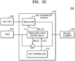
- FIGS. 2A through 2C are block diagrams of a wireless communication device 200 including an NFC integrated circuit 210, according to an example embodiment of the inventive concepts.
- the wireless communication device 200 may include the NFC integrated circuit 210, a secure element 220, a battery 240, and a PMIC 250.
- the NFC integrated circuit 210 may include a power supply path control circuit 212, a regulator 214, and a first switch element SW1.
- the regulator 214 may be implemented as a low dropout (LDO) circuit.
- the regulator 214 may be connected to the battery 240 and may regulate a second supply voltage provided from the battery 240 to an operating voltage of the secure element 220.
- the power supply path control circuit 212 may control a first power supply path through which a first supply voltage from the PMIC 250 is applied to the secure element 220 and a second power supply path through which the second supply voltage from the battery 240 is applied to the secure element 220.
- the second power supply path may include a path through which the second supply voltage regulated by the regulator 214 is provided from the regulator 214 to the secure element 220.
- the power supply path control circuit 212 may provide a switching control signal SW_CS to the first switch element SW1 to control the formation or cutoff of the first power supply path.
- the power supply path control circuit 212 may provide a turn-off control signal to the first switch element SW1 to cut off the first power supply path and provide a turn-on control signal to the first switch element SW1 to form the first power supply path.
- the power supply path control circuit 212 may provide an enable/disable control signal RG_CS to the regulator 214 to control the formation or cut off of the second power supply path.
- the power supply path control circuit 212 may provide a disable control signal to the regulator 214 to cut off the second power supply path and provide an enable control signal to the regulator 214 to form the second power supply path.
- the NFC integrated circuit 210 may further include a second switch element SW2 as compared to the NFC integrated circuit 210 of FIG. 2A .
- the configuration of the NFC integrated circuit 210, except for the second switch element SW2, has been described with reference to FIG. 2A above, and thus detailed descriptions thereof will be omitted.
- the power supply path control circuit 212 may provide a second switching control signal SW_CS2 to the second switch element SW2 to control the formation or cutoff of the second power supply path (i.e., a supply path of a second supply voltage between the battery 240 and the secure element 220).
- the power supply path control circuit 212 may provide a turn-off control signal to the second switch element SW2 to cut off the second power supply path and provide a turn-on control signal to the second switch element SW2 to form the second power supply path.
- power supply path control methods described with reference to FIGS. 2A and 2B are just example embodiments, and the inventive concepts are not limited thereto.
- a power supply path may be controlled using various methods. Controlling the first switch element SW1 using a first switching control signal SW_CS 1 is the same as or similar to controlling the first switch element SW1 of FIG. 2A , and thus, a detailed description thereof will be omitted.
- the NFC integrated circuit 210 may further include an NFC controller 216 as compared to the NFC integrated circuit 210 of FIG. 2A .
- the configuration of the NFC integrated circuit 210, except for the NFC controller 216, has been described with reference to FIG. 2A above, and thus detailed descriptions thereof will be omitted.
- the NFC controller 216 may control all operations of the NFC integrated circuit 210.
- the NFC controller 216 may include a central processing unit (CPU) (not shown), a timer (not shown), etc.
- the CPU may perform an operation and input/output control for the NFC operation of the NFC integrated circuit 210.
- the NFC controller 216 may directly control the formation or cutoff of the first power supply path and the second power supply path regardless of the operation of the power supply path control circuit 212.
- the NFC controller 216 may provide a direct control signal D_CS to the power supply path control circuit 212, and the power supply path control circuit 212 may generate the switching control signal SW_CS or the enable/disable control signal RG_CS based on the direct control signal D_CS.
- the NFC controller 216 may test whether power is properly supplied to the secure element 220 through the first power supply path and the second power supply path. For this test, the NFC controller 216 may provide the direct control signal D_CS to the power supply path control circuit 212.
- the NFC controller 216 may enable or disable the power supply path control circuit 212 and thus selectively use the function of the power supply path control circuit 212.
- the schematic configuration of the NFC integrated circuit 210 has been described with reference to FIGS. 2A through 2C .
- the operation of the power supply path control circuit 212 will be described with reference to FIGS. 3A through 4C .
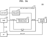
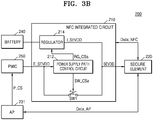
- FIGS. 3A through 3D are diagrams for explaining the operation of the power supply path control circuit 212.
- the configuration of the wireless communication device 200 has been described with reference to FIGS. 2A through 2C above, and thus detailed descriptions thereof will be omitted.
- an AP 231 may communicate with the secure element 220 to exchange security data Data_AP with the secure element 220 and may provide a power control signal P_CS to the PMIC 250 to provide power for the communication to the secure element 220. Since the NFC integrated circuit 210 is not performing an NFC operation and, furthermore, is not communicating with the secure element 220, the NFC integrated circuit 210 may be in an off-state (or an idle state) and the regulator 214 may be in a disabled state.
- the PMIC 250 may provide the NFC integrated circuit 210 with a first supply voltage E_SEVDD corresponding to an operating voltage of the secure element 220 in response to the power control signal P_CS.
- the NFC integrated circuit 210 may bypass the first supply voltage E_SEVDD to be provided to the secure element 220 as an input voltage SEVDD.
- the NFC integrated circuit 210 may turn on the first switch element SW1 in advance to bypass the first supply voltage E_SEVDD.
- the first switch element SW1 may be referred to as a bypass switch.
- the secure element 220 may communicate with the AP 231 using power supplied from the PMIC 250.
- the NFC integrated circuit 210 when the NFC integrated circuit 210 is requested to perform an NFC operation or to communicate with the secure element 220, the NFC integrated circuit 210 may be changed from an off-state (or an idle state) into an on-state (or an operating state).
- the power supply path control circuit 212 may provide a turn-off control signal SW_CSa to the first switch element SW1 to cut off the first power supply path.
- the power supply path control circuit 212 may form the second power supply path as a path for supplying power to the secure element 220.
- the power supply path control circuit 212 may detect existence or non-existence of the first supply voltage E_SEVDD provided from the PMIC 250 and form the second power supply path based on the detection result. Since the NFC integrated circuit 210 currently communicates with the secure element 220, the power supply path control circuit 212 may provide an enable control signal RG_CSa to the regulator 214 to form the second power supply path.
- the power supply path control circuit 212 may detect existence or non-existence of the first supply voltage E_SEVDD provided from the PMIC 250 and determine whether to maintain the second power supply path, which has been formed, based on the detection result.
- the regulator 214 may be connected to the battery 240 and may receive and regulate a second supply voltage.
- the NFC integrated circuit 210 may provide, as the input voltage SEVDD, a regulated second supply voltage I_SEVDD to the secure element 220 through the second power supply path.
- the secure element 220 may communicate with the AP 231 to exchange the security data Data_AP and simultaneously communicate with the NFC integrated circuit 210 to exchange security data Data NFC, using power supplied from the regulator 214.
- Communication between the secure element 220 and the AP 231 and communication between the secure element 220 and the NFC integrated circuit 210 may be sequentially performed according to a desired (or, alternatively, a predetermined) order of priority.
- FIG. 3C is a diagram for explaining a method of supplying power to a secure element using a conventional NFC integrated circuit. It is assumed that the conventional NFC integrated circuit does not include a separate hardware or software component, such as a power supply path control circuit according to example embodiments of the inventive concepts, and a power supply path to the secure element may be controlled by an NFC controller. It is also assumed that communication between the secure element and the conventional NFC integrated circuit is requested during communication between the secure element and an AP.
- the NFC controller may control the power supply path such that the first supply voltage E_SEVDD from a PMIC is applied to the secure element during a first interval INT1 between a time point t1 and a time point t3.
- the NFC controller may control the power supply path such that a regulated second supply voltage from a regulator is applied to the secure element during a second interval INT2 between a time point t2 and a time point t4.
- the NFC controller may control the power supply path such that the first supply voltage E_SEVDD and the regulated second power supply voltage are applied to the secure element during an overlapping interval INT_OL between the first interval INT1 and the second interval INT2.
- the overlapping interval INT_OL may be defined as a change interval for changing a power source which supplies power to the secure element.
- the power source may be changed from the PMIC to the regulator (or a battery).
- the AP may command the PMIC to stop power supply to the secure element, and therefore, the first supply voltage E_SEVDD from the PMIC may not be applied to the conventional NFC integrated circuit at the time point "td”.
- a supply voltage drop VD may occur in the secure element since power supply paths in the conventional NFC integrated circuit have the configuration of connected circuits.
- An unstable supply voltage may be unexpectedly applied to the secure element during the change interval INT_OL, and the unstable supply voltage may cause an operational error in the secure element.
- FIG. 3D is a diagram for explaining a method of supplying power to a secure element using an NFC integrated circuit, according to embodiments of the inventive concepts.
- FIG. 3D will be described with reference to FIG. 3A or 3B . It is assumed that communication between the secure element 220 and the NFC integrated circuit 210 is requested during communication between the secure element 220 and the AP 231.
- the power supply path control circuit 212 may control the first power supply path such that the first supply voltage E_SEVDD from the PMIC 250 is applied to the secure element 220 during a first interval INT1' between a time point t1' and a time point t2'.
- the time point t2' may denote a time when communication between the secure element 220 and the NFC integrated circuit 210 is requested or a time when a desired (or, alternatively, a predetermined) time period has elapsed since the request of the communication between the secure element 220 and the NFC integrated circuit 210.
- the power supply path control circuit 212 may cut off the first power supply path by turning off the first switch element SW1 at the time point t2'.
- the time point t2' may be defined as a switching control time t_SWCNT at which turn-off of the first switch element SW1 is controlled.
- the power supply path control circuit 212 may detect that the first supply voltage E_SEVDD is applied to the NFC integrated circuit 210 through a terminal of the NFC integrated circuit 210 connected to the PMIC 250 and may enable the regulator 214 at the time point t2' based on the detection result such that the regulated second supply voltage I_SEVDD is applied to the secure element 220 during a second interval INT2' between the time point t2' and a time point t3'.
- a power source supplying power to the secure element 220 is changed by the operation of the power supply path control circuit 212 in advance of an occurrence of an unexpected event, so that collision or bad influence between power supplied from the PMIC 250 and power supplied from the regulator 214 (or the battery 240) may be prevented.
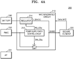
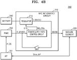
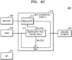
- FIGS. 4A through 4C are diagrams for explaining the operation of the power supply path control circuit 212.
- the configuration of the wireless communication device 200 has been described with reference to FIGS. 2A through 2C above, and thus the detailed descriptions thereof will be omitted.
- the NFC integrated circuit 210 is in the on-state (or the operating state) and may communicate with the secure element 220 to exchange the security data Data_NFC.
- the power supply path control circuit 212 may provide the enable control signal RG_CSa to the regulator 214.
- the power supply path control circuit 212 may also provide the turn-off control signal SW_CSa to the first switch element SW1 to cut off the first power supply path in advance.
- the AP 231 is not communicating with the secure element 220, and the PMIC 250 may not apply a first supply voltage to the NFC integrated circuit 210.
- the regulator 214 may be enabled in response to the enable control signal RG_CSa and may regulate a second supply voltage received from the battery 240 to an operating voltage of the secure element 220.
- the power supply path control circuit 212 may form the second power supply path by enabling the regulator 214.
- the regulator 214 may provide the regulated second supply voltage I_SEVDD to the secure element 220 as the input voltage SEVDD.
- the NFC integrated circuit 210 is in the on-state (or the operating state), and the communication between the NFC integrated circuit 210 and the secure element 220, which has been described with reference to FIG. 4A , may have been completed.
- the AP 231 may communicate with the secure element 220 to exchange the security data Data AP and provide the power control signal P_CS to the PMIC 250 to provide power for the communication to the secure element 220.
- the PMIC 250 may provide the first supply voltage E_SEVDD, which corresponds to the operating voltage of the secure element 220, to the NFC integrated circuit 210 in response to the power control signal P_CS.
- the power supply path control circuit 212 may detect existence or non-existence of the first supply voltage E_SEVDD provided from the PMIC 250 and form the second power supply path based on the detection result.
- the power supply path control circuit 212 may detect that the PMIC 250 currently applies the first supply voltage E_SEVDD to the NFC integrated circuit 210, using a voltage at a terminal of the NFC integrated circuit 210 connected to the PMIC 250. According to the detection, the power supply path control circuit 212 may form the second power supply path by providing the enable control signal RG_CSa to the regulator 214.
- the power supply path control circuit 212 may not separately provide the enable control signal RG_CSa to the regulator 214 but may control the second power supply path which has been formed to be maintained.
- the NFC integrated circuit 210 may provide, as the input voltage SEVDD, the regulated second supply voltage I_SEVDD from the regulator 214 to the secure element 220 through the second power supply path.
- the secure element 220 may communicate with the AP 231 to exchange the security data Data AP, using power supplied from the regulator 214.
- the NFC integrated circuit 210 when the NFC integrated circuit 210 does not perform the NFC operation or does not communicate with the secure element 220 for a desired (or, alternatively, a predetermined) time period, the NFC integrated circuit 210 may be changed from the on-state (or the operating state) into the off-state (or the idle state). Before the NFC integrated circuit 210 is changed into the off-state (or the idle state), the power supply path control circuit 212 may form the first power supply path by providing a turn-on control signal SW_CSb to the first switch element SW1. The power supply path control circuit 212 may also cut off the second power supply path by providing a disable control signal RG_CSb to the regulator 214.
- the NFC integrated circuit 210 may bypass the first supply voltage from the PMIC 250 to the secure element 220 in the off-state (or the idle state).
- FIG. 5 is a block diagram of the configuration of a power supply path control circuit 310 according to an example embodiment of the inventive concepts.
- an NFC integrated circuit 300 may include the power supply path control circuit 310, an NFC controller 320, a regulator 330, and a bypass switch 340.
- the power supply path control circuit 310 may include a regulator control circuit 312 and a bypass switch control circuit 314.
- the bypass switch 340 may be implemented by a transistor.
- the bypass switch 340 is implemented by a P-channel metal-oxide semiconductor (PMOS) transistor.
- the regulator control circuit 312 may generate the enable/disable control signal RG_CS for controlling enable/disable of the regulator 330 and provide the enable/disable control signal RG_CS to the regulator 330 to control a second power supply path.
- the bypass switch control circuit 314 may generate the switching control signal SW_CS for controlling on/off of the bypass switch 340 and provide the switching control signal SW_CS to the bypass switch 340 to control a first power supply path.
- the NFC controller 320 may provide the power supply path control circuit 310 with a sync control signal SYNC_CS for controlling enable/disable of the power supply path control circuit 310.
- the NFC controller 320 may provide the sync control signal SYNC CS at a high level to use the function of the power supply path control circuit 310 when the NFC integrated circuit 300 is in an on-state (or an operating state).
- the NFC controller 320 may provide the sync control signal SYNC_CS at a low level to the power supply path control circuit 310.
- the power supply path control circuit 310 may perform a power supply path control operation.
- the NFC controller 320 may directly perform the power supply path control operation.
- the configuration of the power supply path control circuit 310 shown in FIG. 5 is just an example embodiment, and the inventive concepts are not limited thereto.
- the regulator control circuit 312 and the bypass switch control circuit 314 may not be implemented as separate circuits but may be integrated into a single circuit.
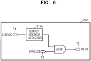
- FIG. 6 is a diagram of the configuration of the regulator control circuit 312 of FIG. 5 , according to an example embodiment of the inventive concepts.
- the regulator control circuit 312 may include first through third terminals T1, T2, and T3, a supply voltage detector 312a, and a first AND gate 312b.
- the supply voltage detector 312a may be connected to the first terminal T1 and may receive the first supply voltage E_SEVDD from an external PMIC.
- the supply voltage detector 312a may detect existence or non-existence of the first supply voltage E_SEVDD through a voltage of the first terminal T1 and output a detection result to the first AND gate 312b.
- the supply voltage detector 312a may output the detection result at a high level when the first supply voltage E_SEVDD has been detected and may output the detection result at a low level when the first supply voltage E_SEVDD has not been detected.
- the first AND gate 312b may be connected to an output terminal of the supply voltage detector 312a and the second and third terminals T2 and T3.
- the first AND gate 312b may receive the sync control signal SYNC_CS from an external NFC controller and receive the detection result from the supply voltage detector 312a.
- the first AND gate 312b may generate the enable/disable control signal RG_CS for a regulator based on the sync control signal SYNC CS and the detection result and output the enable/disable control signal RG_CS to the regulator through the third terminal T3.
- the first AND gate 312b when the first AND gate 312b receives the sync control signal SYNC_CS at the low level, the first AND gate 312b always outputs the enable/disable control signal RG_CS at the low level, and therefore, the function of the regulator control circuit 312 is not used. At this time, the regulator control circuit 312 may be defined as being in a disabled state. When the first AND gate 312b receives the sync control signal SYNC_CS at the high level, the first AND gate 312b outputs the enable/disable control signal RG_CS at a different level according to the detection result, and therefore, the function of the regulator control circuit 312 is used. At this time, the regulator control circuit 312 may be defined as being in an enabled state.
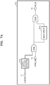
- FIG. 7A is a diagram of the configuration of the regulator control circuit 312 different from the one shown in FIG. 6 .
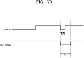
- FIG. 7B is a diagram for explaining the operation of a mask circuit 312c.
- the regulator control circuit 312 may further include a mask circuit 312c and a second AND gate 312d compared to the regulator control circuit 312 of FIG. 6 .
- the mask circuit 312c may be connected to an output terminal of the first AND gate 312b and an input terminal of the second AND gate 312d.
- the mask circuit 312c may operate to increase the width of a particular level interval of the enable/disable control signal RG_CS.
- the mask circuit 312c may receive a mask input signal IN_MASK from the first AND gate 312b. In an embodiment, the mask circuit 312c may increase the width of a first low-level interval INT3 of the mask input signal IN_MASK to the width of a second low-level interval INT3'.
- the mask circuit 312c may increase the width of the first low-level interval INT3, in which the mask input signal IN_MASK is maintained at a low level starting from an edge where the mask input signal IN_MASK transits from a high level to the low level, to generate a mask output signal OUT_MASK including a second low-level interval INT3' in which the mask output signal OUT_MASK is maintained at the low level longer than the mask input signal IN_MASK.
- the mask circuit 312c may control the width of the second low-level interval INT3' and may bypass the mask input signal IN_MASK when the function of the mask circuit 312c is not used.
- the mask circuit 312c may perform a power supply operation meeting the power reset condition for the secure element by converting the mask input signal IN_MASK into the mask output signal OUT_MASK.
- the mask circuit 312c may control the width of the second low-level interval INT3' to correspond to the power reset condition, i.e., the reference time period.
- the second AND gate 312d may be connected to the output terminal of the first AND gate 312b and an output terminal of the mask circuit 312c.
- the second AND gate 312d may output the enable/disable control signal RG_CS through the third terminal T3 based on an output signal of the first AND gate 312b and an output signal of the mask circuit 312c.
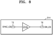
- FIG. 8 is a diagram of the configuration of the bypass switch control circuit 314 of FIG. 5 , according to an example embodiment of the inventive concepts.
- the bypass switch control circuit 314 may include a fifth terminal T5, a sixth terminal T6, and a signal buffer 314a.
- An input terminal of the signal buffer 314a may be connected to the fifth terminal T5 and an output terminal of the signal buffer 314a may be connected to the sixth terminal T6.
- the signal buffer 314a may receive the sync control signal SYNC_CS from an external NFC controller through the fifth terminal T5.
- the signal buffer 314a may buffer the sync control signal SYNC CS and output the switching control signal SW_CS to a bypass switch through the sixth terminal T6.
- the signal buffer 314a may output the switching control signal SW_CS at a low level, so that the bypass switch implemented by a PMOS transistor remains turned on, and therefore, the function of the bypass switch control circuit 314 is not used.
- the bypass switch control circuit 314 may be defined as being in a disabled state.
- the signal buffer 314a may output the switching control signal SW_CS at a high level, so that the bypass switch implemented by a PMOS transistor remains turned on, and therefore, the function of the bypass switch control circuit 314 is used.
- the bypass switch control circuit 314 may be defined as being in an enabled state.
- FIG. 9 is a block diagram of the configuration of a power supply path control circuit 410 according to an example embodiment of the inventive concepts.
- the configuration of an NFC integrated circuit 400 of FIG. 9 has been described in detail with reference to FIG. 5 . Thus, descriptions will be focused on differences between the configuration of FIG. 9 and the configuration of FIG. 5 .
- an NFC controller 420 may provide first and second internal control signals CS_INTa and CS_INTb to the power supply path control circuit 410 and directly control the operations of a regulator control circuit 412 and a bypass switch control circuit 414.
- the NFC controller 420 may test whether power is properly supplied to a secure element through a first power supply path and a second power supply path. For this test, the NFC controller 420 may provide the first and second internal control signals CS_INTa and CS_INTb to the power supply path control circuit 410.
- FIG. 10 is a diagram of the configuration of the regulator control circuit 412 of FIG. 9 , according to an example embodiment of the inventive concepts.
- the configuration of the regulator control circuit 412 of FIG. 10 has been described in detail with reference to FIG. 6 . Thus, descriptions will be focused on differences between the configuration of FIG. 10 and the configuration of FIG. 6 .
- the regulator control circuit 412 may further include a fourth terminal T4 and an OR gate 412c compared to the regulator control circuit 312 of FIG. 6 .
- the OR gate 412c may be connected to an output terminal of a first AND gate 412b and the third and fourth terminals T3 and T4.
- the OR gate 412c may receive the first internal control signal CS_INTa and an output signal of the first AND gate 412b.
- the OR gate 412c may output the enable/disable control signal RG_CS according to the first internal control signal CS_INTa regardless of the output signal of the first AND gate 412b.
- FIG. 11 is a diagram of the configuration of the bypass switch control circuit 414 of FIG. 9 , according to an example embodiment of the inventive concepts.
- the configuration of the bypass switch control circuit 414 of FIG. 11 has been described in detail with reference to FIG. 8 . Thus, descriptions will be focused on differences between the configuration of FIG. 11 and the configuration of FIG. 8 .
- the bypass switch control circuit 414 may further include a seventh terminal T7 and an OR gate 414a compared to the bypass switch control circuit 314 of FIG. 8 .
- the bypass switch control circuit 414 may include a signal buffer.
- the OR gate 414a may be connected to the fifth through seventh terminals T5 through T7.
- the OR gate 414a may receive the sync control signal SYNC_CS through the fifth terminal T5 and the second internal control signal CS_INTb through the seventh terminal T7.
- the OR gate 414a may output the switching control signal SW_CS according to the second internal control signal CS_INTb regardless of the sync control signal SYNC_CS.
- FIGS. 6 , 7A , 8 , 10 , and 11 The configurations of a power supply path control circuit, which are respectively shown in FIGS. 6 , 7A , 8 , 10 , and 11 , are just example embodiments, and the inventive concepts are not limited thereto. It is apparent that the power supply path control circuit may be implemented in various configurations.
- FIGS. 12A and 12B are diagrams for explaining the operation of a wireless communication device 500, according to an example embodiment of the inventive concepts.
- the wireless communication device 500 may include an NFC integrated circuit 510, a secure element 520, and a PMIC 550.
- a power supply path control circuit 512 may transmit power from the PMIC 550 to the secure element 520 through a first power supply path or power from a regulator 514 to the secure element 520 through a second power supply path.
- the power supply path control circuit 512 may turn on a bypass switch 516 to bypass a first supply voltage Vi having a first waveform WFi, which is provided from the PMIC 550 through the first power supply path, to the secure element 520.
- a waveform WF 3 of an input voltage V 3 provided from the NFC integrated circuit 510 to the secure element 520 may be the same as or similar to the first waveform WFi of the first supply voltage Vi.
- the power supply path control circuit 512 may turn off the bypass switch 516 and enable or disable the regulator 514 based on the first supply voltage Vi applied from the PMIC 550.
- the power supply path control circuit 512 may provide a second supply voltage V 2 having a second waveform WF 2 from the regulator 514 to the secure element 520 through the second power supply path by enabling the regulator 514 when the first supply voltage Vi is detected. Accordingly, the waveform WF 3 of the input voltage V 3 provided from the NFC integrated circuit 510 to the secure element 520 may be the same as or similar to the second waveform WF 2 of the second supply voltage V 2 .
- FIG. 13 is a block diagram of an electronic system 1000 according to an example embodiment of the inventive concepts.
- the electronic system 1000 may include an AP 1100, an NFC device 1200, a memory device 1300, a user interface 1400, and a power supply 1500.
- the electronic system 1000 may be a mobile system such as a portable phone, a smartphone, a personal digital assistant (PDA), a portable multimedia player (PMP), a digital camera, a music player, a portable game console, a navigation system, or a laptop computer.
- PDA personal digital assistant
- PMP portable multimedia player
- digital camera a music player
- portable game console a portable game console
- navigation system or a laptop computer.
- the AP 1100 may control all operations of the electronic system 1000.
- the AP 1100 may execute applications providing internet browsers, games, moving pictures, etc.
- the AP 1100 may include a single core or multiple cores.
- the memory device 1300 may store data for the operations of the electronic system 1000.
- the memory device 1300 may store, for example, a boot image for booting the electronic system 1000, output data to be transmitted to an external device, and input data received from the external device.
- the NFC device 1200 may transmit the output data stored in the memory device 1300 to the external device and receive the input data from the external device through NFC and may store the input data in the memory device 1300.
- the NFC device 1200 may include a power supply path control circuit 1210 according to an example embodiment of the inventive concepts.
- the power supply path control circuit 1210 may control a power supply path to an internal device (e.g., a secure element) of the NFC device 1200 based on the state of the NFC device 1200 or existence or non-existence of a supply voltage provided from the power supply 1500 such that stable power may be supplied to the internal device.
- the units and/or devices described above such as the components of the wireless communication device including the NFC integrated circuit and the power supply path control circuit, the regulator and the NFC controller included therein as well as the sub-components of the power supply path control circuit including the regulator control circuit and bypass switch control circuit may be implemented using hardware, a combination of hardware and software, or a non-transitory storage medium storing software that is executable to perform the functions of the same.
- other components of the wireless communication device including the secure element and the AP may also be implemented using hardware, a combination of hardware and software, or a non-transitory storage medium storing software that is executable to perform the functions of the same.
- Hardware may be implemented using processing circuity such as, but not limited to, one or more processors, one or more Central Processing Units (CPUs), one or more controllers, one or more arithmetic logic units (ALUs), one or more digital signal processors (DSPs), one or more microcomputers, one or more field programmable gate arrays (FPGAs), one or more System-on-Chips (SoCs), one or more programmable logic units (PLUs), one or more microprocessors, one or more Application Specific Integrated Circuits (ASICs), or any other device or devices capable of responding to and executing instructions in a defined manner.
- processing circuity such as, but not limited to, one or more processors, one or more Central Processing Units (CPUs), one or more controllers, one or more arithmetic logic units (ALUs), one or more digital signal processors (DSPs), one or more microcomputers, one or more field programmable gate arrays (FPGAs), one or more System-on-Chips (
- Software may include a computer program, program code, instructions, or some combination thereof, for independently or collectively instructing or configuring a hardware device to operate as desired.
- the computer program and/or program code may include program or computer-readable instructions, software components, software modules, data files, data structures, etc., capable of being implemented by one or more hardware devices, such as one or more of the hardware devices mentioned above.
- Examples of program code include both machine code produced by a compiler and higher level program code that is executed using an interpreter.
- a hardware device is a computer processing device (e.g., one or more processors, CPUs, controllers, ALUs, DSPs, microcomputers, microprocessors, etc.)
- the computer processing device may be configured to carry out program code by performing arithmetical, logical, and input/output operations, according to the program code.
- the computer processing device may be programmed to perform the program code, thereby transforming the computer processing device into a special purpose computer processing device.
- the processor becomes programmed to perform the program code and operations corresponding thereto, thereby transforming the processor into a special purpose processor.
- the hardware device may be an integrated circuit customized into special purpose processing circuitry (e.g., an ASIC).
- a hardware device such as a computer processing device, may run an operating system (OS) and one or more software applications that run on the OS.
- the computer processing device also may access, store, manipulate, process, and create data in response to execution of the software.
- OS operating system
- a hardware device may include multiple processing elements and multiple types of processing elements.
- a hardware device may include multiple processors or a processor and a controller.
- other processing configurations are possible, such as parallel processors.
- Software and/or data may be embodied permanently or temporarily in any type of storage media including, but not limited to, any machine, component, physical or virtual equipment, or computer storage medium or device, capable of providing instructions or data to, or being interpreted by, a hardware device.
- the software also may be distributed over network coupled computer systems so that the software is stored and executed in a distributed fashion.
- software and data may be stored by one or more computer readable recording mediums, including tangible or non-transitory computer-readable storage media as discussed herein.
- Storage media may also include one or more storage devices at units and/or devices according to one or more example embodiments.
- the one or more storage devices may be tangible or non-transitory computer-readable storage media, such as random access memory (RAM), read only memory (ROM), a permanent mass storage device (such as a disk drive), and/or any other like data storage mechanism capable of storing and recording data.
- the one or more storage devices may be configured to store computer programs, program code, instructions, or some combination thereof, for one or more operating systems and/or for implementing the example embodiments described herein.
- the computer programs, program code, instructions, or some combination thereof may also be loaded from a separate computer readable storage medium into the one or more storage devices and/or one or more computer processing devices using a drive mechanism.
- a separate computer readable storage medium may include a Universal Serial Bus (USB) flash drive, a memory stick, a Blu-ray/DVD/CD-ROM drive, a memory card, and/or other like computer readable storage media.
- the computer programs, program code, instructions, or some combination thereof may be loaded into the one or more storage devices and/or the one or more computer processing devices from a remote data storage device via a network interface, rather than via a computer readable storage medium.
- the computer programs, program code, instructions, or some combination thereof may be loaded into the one or more storage devices and/or the one or more processors from a remote computing system that is configured to transfer and/or distribute the computer programs, program code, instructions, or some combination thereof, over a network.
- the remote computing system may transfer and/or distribute the computer programs, program code, instructions, or some combination thereof, via a wired interface, an air interface, and/or any other like medium.
- the one or more hardware devices, the storage media, the computer programs, program code, instructions, or some combination thereof, may be specially designed and constructed for the purposes of the example embodiments, or they may be known devices that are altered and/or modified for the purposes of example embodiments.
Landscapes
- Engineering & Computer Science (AREA)
- Theoretical Computer Science (AREA)
- Computer Networks & Wireless Communication (AREA)
- Physics & Mathematics (AREA)
- General Physics & Mathematics (AREA)
- Computer Hardware Design (AREA)
- Microelectronics & Electronic Packaging (AREA)
- Power Engineering (AREA)
- Signal Processing (AREA)
- General Engineering & Computer Science (AREA)
- Power Sources (AREA)
- Semiconductor Integrated Circuits (AREA)
Description
- Example embodiments of the inventive concepts relate to a near field communication (NFC) integrated circuit. For example, at least some example embodiments relate to an NFC integrated circuit for stably supplying power to a device communicating with the NFC integrated circuit and/or a wireless communication device including the NFC integrated circuit.
- A wireless communication device may include an NFC integrated circuit and at least one internal device (e.g., a secure element) supporting NFC to perform NFC with an external device. The internal device may communicate with the NFC integrated circuit so as to transmit and receive data for NFC with the external device.
- To facilitate communication between the internal device and the NFC integrated circuit using NFC, power may be immediately supplied to the internal device through the NFC integrated circuit so that the internal device may communicate with the NFC integrated circuit.
-
US 2013/332756 A1 discloses a near field communication device including an RF power unit that generates an RF power supply voltage through wireless communication with an external communication device, a power detecting unit that detects an output level of a battery connected to the near field communication device, a driving control unit that controls the near field communication device, and a switching control unit that controls a supply of a power supply voltage to the driving control unit from the RF power unit or the battery. The switching control unit controls the supply of the power supply voltage based on at least one of the output level of the battery, a power on/off state of an electronic apparatus including the near field communication device, whether the electronic apparatus is connected to the battery, and whether the RF power supply voltage is generated. -
US 2017/212574 A1 discloses an electronic device including a first connector including a first pin and a second pin configured to connect with a first external electronic device, a second connector configured to connect with a second external electronic device, a connection sensing circuit configured to sense a connection or disconnection of the second external electronic device coupled to the first pin via the second connector, and a switch configured to supply power received from the first external electronic device via the second pin to the first pin if the disconnection is sensed via the connection sensing circuit. - However, conventionally, to facilitate communication between the internal device and a processor (e.g., an application processor) of the wireless communication device other than the NFC integrated circuit, power may be supplied to the internal device under the control of the processor. Accordingly, when the NFC integrated circuit and the processor need to simultaneously or sequentially communicate with the internal device, powers supplied to the internal device may collide with each other or constant power may not be supplied to the internal device. As a result, reliable operation of the internal device may not be secured.
- Example embodiments of the inventive concepts provide a near field communication (NFC) integrated circuit for controlling a power supply path to an internal device to secure the reliable operation of the internal device and/or a wireless communication device including the NFC integrated circuit
- The invention is defined by the independent claim 1. Preferred embodiments of the invention are stipulated in the dependent claims. While several embodiments and/or examples have been disclosed in the description, the subject matter for which protection is sought is strictly and solely limited to those embodiments and/or examples encompassed by the scope of the appended claims. Embodiments and/ or examples mentioned in the description that do not fall under the scope of the claims are useful for understanding the invention.
- Example embodiments of the inventive concepts will be more clearly understood from the following detailed description taken in conjunction with the accompanying drawings in which:
-
FIG. 1 is a block diagram of a wireless communication device according to an example embodiment of the inventive concepts; -
FIGS. 2A through 2C are block diagrams of a wireless communication device including a near field communication (NFC) integrated circuit, according to an example embodiment of the inventive concepts; -
FIGS. 3A through 3D are diagrams for explaining the operation of a power supply path control circuit; -
FIGS. 4A through 4C are diagrams for explaining the operation of a power supply path control circuit; -
FIG. 5 is a block diagram of the configuration of a power supply path control circuit according to an example embodiment of the inventive concepts; -
FIG. 6 is a diagram of the configuration of a regulator control circuit ofFIG. 5 , according to an example embodiment of the inventive concepts; -
FIG. 7A is a diagram of the configuration of a regulator control circuit different from the one shown inFIG. 6 ; -
FIG. 7B is a diagram for explaining the operation of a mask circuit; -
FIG. 8 is a diagram of the configuration of a bypass switch control circuit ofFIG. 5 , according to an example embodiment of the inventive concepts; -
FIG. 9 is a block diagram of the configuration of a power supply path control circuit according to an example embodiment of the inventive concepts; -
FIG. 10 is a diagram of the configuration of a regulator control circuit ofFIG. 9 , according to an example embodiment of the inventive concepts; -
FIG. 11 is a diagram of the configuration of a bypass switch control circuit ofFIG. 9 , according to an example embodiment of the inventive concepts; -
FIGS. 12A and12B are diagrams for explaining the operation of a wireless communication device, according to an example embodiment of the inventive concepts; and -
FIG. 13 is a block diagram of an electronic system according to an example embodiment of the inventive concepts. -
FIG. 1 is a block diagram of awireless communication device 100 according to an example embodiment of the inventive concepts. Although a mobile communication terminal is described as an example with reference toFIG. 1 , the inventive concepts are not limited thereto, and thewireless communication device 100 may include a near field communication (NFC) device. Furthermore, it will be understood that the concept of thewireless communication device 100 covers any electronic device which wirelessly communicates with an external communication device. - Referring to
FIG. 1 , thewireless communication device 100 includes an NFC integratedcircuit 110, aninternal device 120,service supporting devices 130, abattery 140, and a power management integrated circuit (PMIC) 150. - The
wireless communication device 100 may communicate with an external communication device AWA using an NFC protocol. - The NFC integrated
circuit 110 is connected to thebattery 140 and performs NFC using power supplied from thebattery 140. - The
internal device 120 is provided to support an NFC operation. Theinternal device 120 may manage data for the NFC operation. Hereinafter, theinternal device 120 is described as including a secure element, but example embodiments of the inventive concepts are not limited thereto. It will be understood that theinternal device 120 includes a device supporting various communication operations apart from the NFC operation. - The
service supporting devices 130 provide various services for a user of thewireless communication device 100. Theservice supporting devices 130 may include an application processor (AP) 131_1, an audio codec 132_2, and a display module 130_n. Theservice supporting devices 130 may communicate with theinternal device 120 to support services. Although descriptions below will be focused on the AP 131_1, the AP 131_1 is just an example, and it is apparent that example embodiments of the inventive concepts may also be applied to the operations between theinternal device 120 and any one of theservice supporting devices 130. - The AP 131_1 may communicate with the
internal device 120 to exchange security data to provide services for a user. For example, the AP 131_1 may communicate with theinternal device 120 based on a serial peripheral interface (SPI). In an example of communication between the AP 131_1 and theinternal device 120, the AP 131_1 may acquire and provide a user's fingerprint information to theinternal device 120 so as to provide a service, for which security is a prerequisite, for the user. Theinternal device 120 may manage the fingerprint information and may provide the fingerprint information stored therein to the AP 131_1 in response to a fingerprint request from the AP 131_1. Theinternal device 120 may be supplied with power, for communication with the AP 131_1, through the NFC integratedcircuit 110. In an example embodiment, the AP 131_1 may control thePMIC 150 such that the power is supplied to theinternal device 120. ThePMIC 150 may apply a supply voltage to the NFC integratedcircuit 110 in response to a request from the AP 131_1, and the NFCintegrated circuit 110 may bypass the supply voltage to theinternal device 120. However, it is just one embodiment and the inventive concepts are not limited thereto. The NFC integratedcircuit 110 may regulate the supply voltage received from thePMIC 150 before providing the supply voltage to theinternal device 120. Hereinafter, a path of power supplied from thePMIC 150 to theinternal device 120 may be defined as a first power supply path. - The NFC
integrated circuit 110 may communicate with theinternal device 120 to exchange security data for an NFC operation. For example, the NFC integratedcircuit 110 may communicate with theinternal device 120 based on a single wired protocol (SWP). The NFCintegrated circuit 110 may provide new security data to theinternal device 120, and theinternal device 120 may manage the new security data. When theinternal device 120 receives a security data request from the NFC integratedcircuit 110, theinternal device 120 may provide security data stored therein to the NFC integratedcircuit 110. Theinternal device 120 may be supplied with power, to communicate with the NFC integratedcircuit 110, through the NFC integratedcircuit 110. In an example embodiment, the NFC integratedcircuit 110 may regulate a supply voltage received from thebattery 140 to an operating voltage of theinternal device 120 and provide the regulated supply voltage to theinternal device 120. Hereinafter, a path of power supplied from thebattery 140 to theinternal device 120 may be defined as a second power supply path. - The NFC
integrated circuit 110 includes a power supplypath control circuit 112. The power supplypath control circuit 112 may control a power supply path through which power is supplied to theinternal device 120. In an example embodiment, the power supplypath control circuit 112 may control a power supply path so as to reduce (or, alternatively, minimize) collision or mutual influence between a supply voltage provided from thePMIC 150 to theinternal device 120 and a supply voltage provided from thebattery 140 to theinternal device 120. - In an embodiment, the power supply
path control circuit 112 efficiently controls a power supply path based on a state of the NFC integratedcircuit 110. When the NFC integratedcircuit 110 is in an on-state (or an operating state), the power supplypath control circuit 112 cuts off the first power supply path and detects a supply voltage provided from thePMIC 150 to the NFC integratedcircuit 110 and forms the second power supply path based on the detection result. Thereafter, the power supplypath control circuit 112 forms the first power supply path and cuts off the second power supply path before the NFC integratedcircuit 110 is changed from the on-state (or the operating state) into an off-state (or an idle state). Accordingly, when the NFC integratedcircuit 110 is in the off-state (or the idle state), the first power supply path may be formed while the second power supply path may be cut off. At this time, the supply voltage received from thePMIC 150 may be bypassed to theinternal device 120. - In an example embodiment, the NFC integrated
circuit 110 may be changed from the off-state into the on-state and perform an NFC operation. When the NFC operation has not been performed for a desired (or, alternatively, a predetermined) time period, the NFC integratedcircuit 110 may be changed from the on-state into the off-state. In another example embodiment, the NFC integratedcircuit 110 may be changed from the idle state into the operating state and perform the NFC operation. When the NFC operation has not been performed for a desired (or, alternatively, a predetermined) time period, the NFC integratedcircuit 110 may be changed from the operating state into the idle state. In the idle state, the NFC integratedcircuit 110 may be on standby, consuming relatively less (or, alternatively, minimum) power, until receiving an NFC request or transmitting the NFC request to an external communication device. In the operating state, the NFC integratedcircuit 110 may perform the NFC operation in response to the NFC request or may transmit the NFC request to the external communication device and perform the NFC operation according to a response from the external communication device. - The power supply
path control circuit 112 may immediately control a supply path of power to theinternal device 120 according to the state of the NFC integratedcircuit 110, thereby reducing (or, alternatively, preventing) collision or a bad influence between powers received through multiple power supply paths. As a result, reliable operation of theinternal device 120 may be secured. -
FIGS. 2A through 2C are block diagrams of awireless communication device 200 including an NFCintegrated circuit 210, according to an example embodiment of the inventive concepts. - Referring to
FIG. 2A , thewireless communication device 200 may include the NFC integratedcircuit 210, asecure element 220, abattery 240, and aPMIC 250. - The NFC
integrated circuit 210 may include a power supplypath control circuit 212, aregulator 214, and a first switch element SW1. Theregulator 214 may be implemented as a low dropout (LDO) circuit. Theregulator 214 may be connected to thebattery 240 and may regulate a second supply voltage provided from thebattery 240 to an operating voltage of thesecure element 220. - In an example embodiment, the power supply
path control circuit 212 may control a first power supply path through which a first supply voltage from thePMIC 250 is applied to thesecure element 220 and a second power supply path through which the second supply voltage from thebattery 240 is applied to thesecure element 220. The second power supply path may include a path through which the second supply voltage regulated by theregulator 214 is provided from theregulator 214 to thesecure element 220. - The power supply
path control circuit 212 may provide a switching control signal SW_CS to the first switch element SW1 to control the formation or cutoff of the first power supply path. For example, the power supplypath control circuit 212 may provide a turn-off control signal to the first switch element SW1 to cut off the first power supply path and provide a turn-on control signal to the first switch element SW1 to form the first power supply path. The power supplypath control circuit 212 may provide an enable/disable control signal RG_CS to theregulator 214 to control the formation or cut off of the second power supply path. For example, the power supplypath control circuit 212 may provide a disable control signal to theregulator 214 to cut off the second power supply path and provide an enable control signal to theregulator 214 to form the second power supply path. - Referring to
FIG. 2B , the NFC integratedcircuit 210 may further include a second switch element SW2 as compared to the NFC integratedcircuit 210 ofFIG. 2A . The configuration of the NFC integratedcircuit 210, except for the second switch element SW2, has been described with reference toFIG. 2A above, and thus detailed descriptions thereof will be omitted. The power supplypath control circuit 212 may provide a second switching control signal SW_CS2 to the second switch element SW2 to control the formation or cutoff of the second power supply path (i.e., a supply path of a second supply voltage between thebattery 240 and the secure element 220). For example, the power supplypath control circuit 212 may provide a turn-off control signal to the second switch element SW2 to cut off the second power supply path and provide a turn-on control signal to the second switch element SW2 to form the second power supply path. However, power supply path control methods described with reference toFIGS. 2A and2B are just example embodiments, and the inventive concepts are not limited thereto. A power supply path may be controlled using various methods. Controlling the first switch element SW1 using a first switching control signal SW_CS 1 is the same as or similar to controlling the first switch element SW1 ofFIG. 2A , and thus, a detailed description thereof will be omitted. - Referring to
FIG. 2C , the NFC integratedcircuit 210 may further include anNFC controller 216 as compared to the NFC integratedcircuit 210 ofFIG. 2A . The configuration of the NFC integratedcircuit 210, except for theNFC controller 216, has been described with reference toFIG. 2A above, and thus detailed descriptions thereof will be omitted. TheNFC controller 216 may control all operations of the NFC integratedcircuit 210. TheNFC controller 216 may include a central processing unit (CPU) (not shown), a timer (not shown), etc. The CPU may perform an operation and input/output control for the NFC operation of the NFC integratedcircuit 210. - In an example embodiment, the
NFC controller 216 may directly control the formation or cutoff of the first power supply path and the second power supply path regardless of the operation of the power supplypath control circuit 212. In detail, theNFC controller 216 may provide a direct control signal D_CS to the power supplypath control circuit 212, and the power supplypath control circuit 212 may generate the switching control signal SW_CS or the enable/disable control signal RG_CS based on the direct control signal D_CS. For example, theNFC controller 216 may test whether power is properly supplied to thesecure element 220 through the first power supply path and the second power supply path. For this test, theNFC controller 216 may provide the direct control signal D_CS to the power supplypath control circuit 212. In addition, theNFC controller 216 may enable or disable the power supplypath control circuit 212 and thus selectively use the function of the power supplypath control circuit 212. - The schematic configuration of the NFC integrated
circuit 210 has been described with reference toFIGS. 2A through 2C . The operation of the power supplypath control circuit 212 will be described with reference toFIGS. 3A through 4C . -
FIGS. 3A through 3D are diagrams for explaining the operation of the power supplypath control circuit 212. The configuration of thewireless communication device 200 has been described with reference toFIGS. 2A through 2C above, and thus detailed descriptions thereof will be omitted. - Referring to
FIG. 3A , anAP 231 may communicate with thesecure element 220 to exchange security data Data_AP with thesecure element 220 and may provide a power control signal P_CS to thePMIC 250 to provide power for the communication to thesecure element 220. Since the NFC integratedcircuit 210 is not performing an NFC operation and, furthermore, is not communicating with thesecure element 220, the NFC integratedcircuit 210 may be in an off-state (or an idle state) and theregulator 214 may be in a disabled state. - The
PMIC 250 may provide the NFC integratedcircuit 210 with a first supply voltage E_SEVDD corresponding to an operating voltage of thesecure element 220 in response to the power control signal P_CS. The NFCintegrated circuit 210 may bypass the first supply voltage E_SEVDD to be provided to thesecure element 220 as an input voltage SEVDD. The NFCintegrated circuit 210 may turn on the first switch element SW1 in advance to bypass the first supply voltage E_SEVDD. The first switch element SW1 may be referred to as a bypass switch. Thesecure element 220 may communicate with theAP 231 using power supplied from thePMIC 250. - Referring to
FIG. 3B , when the NFC integratedcircuit 210 is requested to perform an NFC operation or to communicate with thesecure element 220, the NFC integratedcircuit 210 may be changed from an off-state (or an idle state) into an on-state (or an operating state). The power supplypath control circuit 212 may provide a turn-off control signal SW_CSa to the first switch element SW1 to cut off the first power supply path. - In an example embodiment, when the NFC integrated
circuit 210 communicates with thesecure element 220, the power supplypath control circuit 212 may form the second power supply path as a path for supplying power to thesecure element 220. When the NFC integratedcircuit 210 does not communicate with thesecure element 220, the power supplypath control circuit 212 may detect existence or non-existence of the first supply voltage E_SEVDD provided from thePMIC 250 and form the second power supply path based on the detection result. Since the NFC integratedcircuit 210 currently communicates with thesecure element 220, the power supplypath control circuit 212 may provide an enable control signal RG_CSa to theregulator 214 to form the second power supply path. Thereafter, when the communication between the NFC integratedcircuit 210 and thesecure element 220 is completed, the power supplypath control circuit 212 may detect existence or non-existence of the first supply voltage E_SEVDD provided from thePMIC 250 and determine whether to maintain the second power supply path, which has been formed, based on the detection result. - The
regulator 214 may be connected to thebattery 240 and may receive and regulate a second supply voltage. The NFCintegrated circuit 210 may provide, as the input voltage SEVDD, a regulated second supply voltage I_SEVDD to thesecure element 220 through the second power supply path. Thesecure element 220 may communicate with theAP 231 to exchange the security data Data_AP and simultaneously communicate with the NFC integratedcircuit 210 to exchange security data Data NFC, using power supplied from theregulator 214. However, this is just an example embodiment, and the inventive concepts are not limited thereto. Communication between thesecure element 220 and theAP 231 and communication between thesecure element 220 and the NFC integratedcircuit 210 may be sequentially performed according to a desired (or, alternatively, a predetermined) order of priority. -
FIG. 3C is a diagram for explaining a method of supplying power to a secure element using a conventional NFC integrated circuit. It is assumed that the conventional NFC integrated circuit does not include a separate hardware or software component, such as a power supply path control circuit according to example embodiments of the inventive concepts, and a power supply path to the secure element may be controlled by an NFC controller. It is also assumed that communication between the secure element and the conventional NFC integrated circuit is requested during communication between the secure element and an AP. - Referring to
FIG. 3C , the NFC controller may control the power supply path such that the first supply voltage E_SEVDD from a PMIC is applied to the secure element during a first interval INT1 between a time point t1 and a time point t3. The NFC controller may control the power supply path such that a regulated second supply voltage from a regulator is applied to the secure element during a second interval INT2 between a time point t2 and a time point t4. To stably supply power to the secure element, the NFC controller may control the power supply path such that the first supply voltage E_SEVDD and the regulated second power supply voltage are applied to the secure element during an overlapping interval INT_OL between the first interval INT1 and the second interval INT2. The overlapping interval INT_OL may be defined as a change interval for changing a power source which supplies power to the secure element. In the change interval INT_OL ofFIG. 3C , the power source may be changed from the PMIC to the regulator (or a battery). However, when a sudden problem occurs in an AP at a time point "td" during the change interval INT_OL or when communication between the AP and the secure element is completed at the time point "td", the AP may command the PMIC to stop power supply to the secure element, and therefore, the first supply voltage E_SEVDD from the PMIC may not be applied to the conventional NFC integrated circuit at the time point "td". When the first supply voltage E_SEVDD is not applied at the time point "td" during the change interval INT_OL, a supply voltage drop VD may occur in the secure element since power supply paths in the conventional NFC integrated circuit have the configuration of connected circuits. An unstable supply voltage may be unexpectedly applied to the secure element during the change interval INT_OL, and the unstable supply voltage may cause an operational error in the secure element. -
FIG. 3D is a diagram for explaining a method of supplying power to a secure element using an NFC integrated circuit, according to embodiments of the inventive concepts.FIG. 3D will be described with reference toFIG. 3A or3B . It is assumed that communication between thesecure element 220 and the NFC integratedcircuit 210 is requested during communication between thesecure element 220 and theAP 231. - Referring to
FIG. 3D , the power supplypath control circuit 212 may control the first power supply path such that the first supply voltage E_SEVDD from thePMIC 250 is applied to thesecure element 220 during a first interval INT1' between a time point t1' and a time point t2'. The time point t2' may denote a time when communication between thesecure element 220 and the NFC integratedcircuit 210 is requested or a time when a desired (or, alternatively, a predetermined) time period has elapsed since the request of the communication between thesecure element 220 and the NFC integratedcircuit 210. The power supplypath control circuit 212 may cut off the first power supply path by turning off the first switch element SW1 at the time point t2'. After the time point t2', the first supply voltage E_SEVDD is not applied to thesecure element 220. The time point t2' may be defined as a switching control time t_SWCNT at which turn-off of the first switch element SW1 is controlled. The power supplypath control circuit 212 may detect that the first supply voltage E_SEVDD is applied to the NFC integratedcircuit 210 through a terminal of the NFC integratedcircuit 210 connected to thePMIC 250 and may enable theregulator 214 at the time point t2' based on the detection result such that the regulated second supply voltage I_SEVDD is applied to thesecure element 220 during a second interval INT2' between the time point t2' and a time point t3'. - As described above, a power source supplying power to the
secure element 220 is changed by the operation of the power supplypath control circuit 212 in advance of an occurrence of an unexpected event, so that collision or bad influence between power supplied from thePMIC 250 and power supplied from the regulator 214 (or the battery 240) may be prevented. -
FIGS. 4A through 4C are diagrams for explaining the operation of the power supplypath control circuit 212. The configuration of thewireless communication device 200 has been described with reference toFIGS. 2A through 2C above, and thus the detailed descriptions thereof will be omitted. - Referring to
FIG. 4A , the NFC integratedcircuit 210 is in the on-state (or the operating state) and may communicate with thesecure element 220 to exchange the security data Data_NFC. To supply power for the communication to thesecure element 220, the power supplypath control circuit 212 may provide the enable control signal RG_CSa to theregulator 214. The power supplypath control circuit 212 may also provide the turn-off control signal SW_CSa to the first switch element SW1 to cut off the first power supply path in advance. TheAP 231 is not communicating with thesecure element 220, and thePMIC 250 may not apply a first supply voltage to the NFC integratedcircuit 210. - The
regulator 214 may be enabled in response to the enable control signal RG_CSa and may regulate a second supply voltage received from thebattery 240 to an operating voltage of thesecure element 220. The power supplypath control circuit 212 may form the second power supply path by enabling theregulator 214. Theregulator 214 may provide the regulated second supply voltage I_SEVDD to thesecure element 220 as the input voltage SEVDD. - Referring to
FIG. 4B , the NFC integratedcircuit 210 is in the on-state (or the operating state), and the communication between the NFC integratedcircuit 210 and thesecure element 220, which has been described with reference toFIG. 4A , may have been completed. TheAP 231 may communicate with thesecure element 220 to exchange the security data Data AP and provide the power control signal P_CS to thePMIC 250 to provide power for the communication to thesecure element 220. - The
PMIC 250 may provide the first supply voltage E_SEVDD, which corresponds to the operating voltage of thesecure element 220, to the NFC integratedcircuit 210 in response to the power control signal P_CS. The power supplypath control circuit 212 may detect existence or non-existence of the first supply voltage E_SEVDD provided from thePMIC 250 and form the second power supply path based on the detection result. The power supplypath control circuit 212 may detect that thePMIC 250 currently applies the first supply voltage E_SEVDD to the NFC integratedcircuit 210, using a voltage at a terminal of the NFC integratedcircuit 210 connected to thePMIC 250. According to the detection, the power supplypath control circuit 212 may form the second power supply path by providing the enable control signal RG_CSa to theregulator 214. However, when theregulator 214 has been enabled, as shown inFIG. 4A , the power supplypath control circuit 212 may not separately provide the enable control signal RG_CSa to theregulator 214 but may control the second power supply path which has been formed to be maintained. - The NFC
integrated circuit 210 may provide, as the input voltage SEVDD, the regulated second supply voltage I_SEVDD from theregulator 214 to thesecure element 220 through the second power supply path. Thesecure element 220 may communicate with theAP 231 to exchange the security data Data AP, using power supplied from theregulator 214. - Referring to
FIG. 4C , when the NFC integratedcircuit 210 does not perform the NFC operation or does not communicate with thesecure element 220 for a desired (or, alternatively, a predetermined) time period, the NFC integratedcircuit 210 may be changed from the on-state (or the operating state) into the off-state (or the idle state). Before the NFC integratedcircuit 210 is changed into the off-state (or the idle state), the power supplypath control circuit 212 may form the first power supply path by providing a turn-on control signal SW_CSb to the first switch element SW1. The power supplypath control circuit 212 may also cut off the second power supply path by providing a disable control signal RG_CSb to theregulator 214. - Thereafter, the NFC integrated
circuit 210 may bypass the first supply voltage from thePMIC 250 to thesecure element 220 in the off-state (or the idle state). -
FIG. 5 is a block diagram of the configuration of a power supplypath control circuit 310 according to an example embodiment of the inventive concepts. - Referring to
FIG. 5 , an NFCintegrated circuit 300 may include the power supplypath control circuit 310, anNFC controller 320, aregulator 330, and abypass switch 340. The power supplypath control circuit 310 may include aregulator control circuit 312 and a bypassswitch control circuit 314. - In an example embodiment, the
bypass switch 340 may be implemented by a transistor. Hereinafter, it is assumed that thebypass switch 340 is implemented by a P-channel metal-oxide semiconductor (PMOS) transistor. Theregulator control circuit 312 may generate the enable/disable control signal RG_CS for controlling enable/disable of theregulator 330 and provide the enable/disable control signal RG_CS to theregulator 330 to control a second power supply path. - The bypass
switch control circuit 314 may generate the switching control signal SW_CS for controlling on/off of thebypass switch 340 and provide the switching control signal SW_CS to thebypass switch 340 to control a first power supply path. - The
NFC controller 320 may provide the power supplypath control circuit 310 with a sync control signal SYNC_CS for controlling enable/disable of the power supplypath control circuit 310. In an embodiment, theNFC controller 320 may provide the sync control signal SYNC CS at a high level to use the function of the power supplypath control circuit 310 when the NFC integratedcircuit 300 is in an on-state (or an operating state). When the function of the power supplypath control circuit 310 is not used during the on-state (or an operating state) of the NFC integratedcircuit 300 or when the NFC integratedcircuit 300 is in an off-state (or an idle state), theNFC controller 320 may provide the sync control signal SYNC_CS at a low level to the power supplypath control circuit 310. In other words, when theNFC controller 320 enables the power supplypath control circuit 310, the power supplypath control circuit 310 may perform a power supply path control operation. When theNFC controller 320 disables the power supplypath control circuit 310, theNFC controller 320 may directly perform the power supply path control operation. - However, the configuration of the power supply
path control circuit 310 shown inFIG. 5 is just an example embodiment, and the inventive concepts are not limited thereto. Theregulator control circuit 312 and the bypassswitch control circuit 314 may not be implemented as separate circuits but may be integrated into a single circuit. -
FIG. 6 is a diagram of the configuration of theregulator control circuit 312 ofFIG. 5 , according to an example embodiment of the inventive concepts. - Referring to
FIG. 6 , theregulator control circuit 312 may include first through third terminals T1, T2, and T3, asupply voltage detector 312a, and a first ANDgate 312b. Thesupply voltage detector 312a may be connected to the first terminal T1 and may receive the first supply voltage E_SEVDD from an external PMIC. Thesupply voltage detector 312a may detect existence or non-existence of the first supply voltage E_SEVDD through a voltage of the first terminal T1 and output a detection result to the first ANDgate 312b. For example, thesupply voltage detector 312a may output the detection result at a high level when the first supply voltage E_SEVDD has been detected and may output the detection result at a low level when the first supply voltage E_SEVDD has not been detected. - The first AND
gate 312b may be connected to an output terminal of thesupply voltage detector 312a and the second and third terminals T2 and T3. The first ANDgate 312b may receive the sync control signal SYNC_CS from an external NFC controller and receive the detection result from thesupply voltage detector 312a. The first ANDgate 312b may generate the enable/disable control signal RG_CS for a regulator based on the sync control signal SYNC CS and the detection result and output the enable/disable control signal RG_CS to the regulator through the third terminal T3. For example, when the first ANDgate 312b receives the sync control signal SYNC_CS at the low level, the first ANDgate 312b always outputs the enable/disable control signal RG_CS at the low level, and therefore, the function of theregulator control circuit 312 is not used. At this time, theregulator control circuit 312 may be defined as being in a disabled state. When the first ANDgate 312b receives the sync control signal SYNC_CS at the high level, the first ANDgate 312b outputs the enable/disable control signal RG_CS at a different level according to the detection result, and therefore, the function of theregulator control circuit 312 is used. At this time, theregulator control circuit 312 may be defined as being in an enabled state. -
FIG. 7A is a diagram of the configuration of theregulator control circuit 312 different from the one shown inFIG. 6 .FIG. 7B is a diagram for explaining the operation of amask circuit 312c. - Referring to
FIG. 7A , theregulator control circuit 312 may further include amask circuit 312c and a second ANDgate 312d compared to theregulator control circuit 312 ofFIG. 6 . Themask circuit 312c may be connected to an output terminal of the first ANDgate 312b and an input terminal of the second ANDgate 312d. Themask circuit 312c may operate to increase the width of a particular level interval of the enable/disable control signal RG_CS. - Referring to
FIG. 7B , themask circuit 312c may receive a mask input signal IN_MASK from the first ANDgate 312b. In an embodiment, themask circuit 312c may increase the width of a first low-level interval INT3 of the mask input signal IN_MASK to the width of a second low-level interval INT3'. Themask circuit 312c may increase the width of the first low-level interval INT3, in which the mask input signal IN_MASK is maintained at a low level starting from an edge where the mask input signal IN_MASK transits from a high level to the low level, to generate a mask output signal OUT_MASK including a second low-level interval INT3' in which the mask output signal OUT_MASK is maintained at the low level longer than the mask input signal IN_MASK. - The
mask circuit 312c may control the width of the second low-level interval INT3' and may bypass the mask input signal IN_MASK when the function of themask circuit 312c is not used. - In a case where a secure element may correctly perform a power reset operation under the condition that a supply voltage is not applied to the secure element for a reference time period, the
mask circuit 312c may perform a power supply operation meeting the power reset condition for the secure element by converting the mask input signal IN_MASK into the mask output signal OUT_MASK. Themask circuit 312c may control the width of the second low-level interval INT3' to correspond to the power reset condition, i.e., the reference time period. - Referring back to
FIG. 7A , the second ANDgate 312d may be connected to the output terminal of the first ANDgate 312b and an output terminal of themask circuit 312c. The second ANDgate 312d may output the enable/disable control signal RG_CS through the third terminal T3 based on an output signal of the first ANDgate 312b and an output signal of themask circuit 312c. -
FIG. 8 is a diagram of the configuration of the bypassswitch control circuit 314 ofFIG. 5 , according to an example embodiment of the inventive concepts. - Referring to
FIG. 8 , the bypassswitch control circuit 314 may include a fifth terminal T5, a sixth terminal T6, and asignal buffer 314a. An input terminal of thesignal buffer 314a may be connected to the fifth terminal T5 and an output terminal of thesignal buffer 314a may be connected to the sixth terminal T6. Thesignal buffer 314a may receive the sync control signal SYNC_CS from an external NFC controller through the fifth terminal T5. Thesignal buffer 314a may buffer the sync control signal SYNC CS and output the switching control signal SW_CS to a bypass switch through the sixth terminal T6. For example, when thesignal buffer 314a receives the sync control signal SYNC_CS at the low level, thesignal buffer 314a may output the switching control signal SW_CS at a low level, so that the bypass switch implemented by a PMOS transistor remains turned on, and therefore, the function of the bypassswitch control circuit 314 is not used. At this time, the bypassswitch control circuit 314 may be defined as being in a disabled state. When thesignal buffer 314a receives the sync control signal SYNC CS at the high level, thesignal buffer 314a may output the switching control signal SW_CS at a high level, so that the bypass switch implemented by a PMOS transistor remains turned on, and therefore, the function of the bypassswitch control circuit 314 is used. At this time, the bypassswitch control circuit 314 may be defined as being in an enabled state. -
FIG. 9 is a block diagram of the configuration of a power supplypath control circuit 410 according to an example embodiment of the inventive concepts. The configuration of an NFCintegrated circuit 400 ofFIG. 9 has been described in detail with reference toFIG. 5 . Thus, descriptions will be focused on differences between the configuration ofFIG. 9 and the configuration ofFIG. 5 . - Referring to
FIG. 9 , anNFC controller 420 may provide first and second internal control signals CS_INTa and CS_INTb to the power supplypath control circuit 410 and directly control the operations of aregulator control circuit 412 and a bypassswitch control circuit 414. For example, theNFC controller 420 may test whether power is properly supplied to a secure element through a first power supply path and a second power supply path. For this test, theNFC controller 420 may provide the first and second internal control signals CS_INTa and CS_INTb to the power supplypath control circuit 410. -
FIG. 10 is a diagram of the configuration of theregulator control circuit 412 ofFIG. 9 , according to an example embodiment of the inventive concepts. The configuration of theregulator control circuit 412 ofFIG. 10 has been described in detail with reference toFIG. 6 . Thus, descriptions will be focused on differences between the configuration ofFIG. 10 and the configuration ofFIG. 6 . - Referring to
FIG. 10 , theregulator control circuit 412 may further include a fourth terminal T4 and anOR gate 412c compared to theregulator control circuit 312 ofFIG. 6 . The ORgate 412c may be connected to an output terminal of a first ANDgate 412b and the third and fourth terminals T3 and T4. The ORgate 412c may receive the first internal control signal CS_INTa and an output signal of the first ANDgate 412b. The ORgate 412c may output the enable/disable control signal RG_CS according to the first internal control signal CS_INTa regardless of the output signal of the first ANDgate 412b. -
FIG. 11 is a diagram of the configuration of the bypassswitch control circuit 414 ofFIG. 9 , according to an example embodiment of the inventive concepts. The configuration of the bypassswitch control circuit 414 ofFIG. 11 has been described in detail with reference toFIG. 8 . Thus, descriptions will be focused on differences between the configuration ofFIG. 11 and the configuration ofFIG. 8 . - Referring to
FIG. 11 , the bypassswitch control circuit 414 may further include a seventh terminal T7 and anOR gate 414a compared to the bypassswitch control circuit 314 ofFIG. 8 . Although not shown inFIG. 11 , the bypassswitch control circuit 414 may include a signal buffer. TheOR gate 414a may be connected to the fifth through seventh terminals T5 through T7. TheOR gate 414a may receive the sync control signal SYNC_CS through the fifth terminal T5 and the second internal control signal CS_INTb through the seventh terminal T7. TheOR gate 414a may output the switching control signal SW_CS according to the second internal control signal CS_INTb regardless of the sync control signal SYNC_CS. - The configurations of a power supply path control circuit, which are respectively shown in
FIGS. 6 ,7A ,8 ,10 , and11 , are just example embodiments, and the inventive concepts are not limited thereto. It is apparent that the power supply path control circuit may be implemented in various configurations. -
FIGS. 12A and12B are diagrams for explaining the operation of awireless communication device 500, according to an example embodiment of the inventive concepts. - Referring to
FIG. 12A , thewireless communication device 500 may include an NFCintegrated circuit 510, asecure element 520, and aPMIC 550. A power supplypath control circuit 512 may transmit power from thePMIC 550 to thesecure element 520 through a first power supply path or power from aregulator 514 to thesecure element 520 through a second power supply path. - AS shown in
FIG. 12A , in some example embodiments, when the NFC integratedcircuit 510 is in an off state (or an idle state), the power supplypath control circuit 512 may turn on abypass switch 516 to bypass a first supply voltage Vi having a first waveform WFi, which is provided from thePMIC 550 through the first power supply path, to thesecure element 520. Accordingly, a waveform WF3 of an input voltage V3 provided from the NFC integratedcircuit 510 to thesecure element 520 may be the same as or similar to the first waveform WFi of the first supply voltage Vi. - Referring to
FIG. 12B , when the NFC integratedcircuit 510 is in an on-state (or an operating state), the power supplypath control circuit 512 may turn off thebypass switch 516 and enable or disable theregulator 514 based on the first supply voltage Vi applied from thePMIC 550. - As shown in
FIG. 12B , in some example embodiments, the power supplypath control circuit 512 may provide a second supply voltage V2 having a second waveform WF2 from theregulator 514 to thesecure element 520 through the second power supply path by enabling theregulator 514 when the first supply voltage Vi is detected. Accordingly, the waveform WF3 of the input voltage V3 provided from the NFC integratedcircuit 510 to thesecure element 520 may be the same as or similar to the second waveform WF2 of the second supply voltage V2. -
FIG. 13 is a block diagram of anelectronic system 1000 according to an example embodiment of the inventive concepts. - Referring to
FIG. 13 , theelectronic system 1000 may include anAP 1100, anNFC device 1200, amemory device 1300, auser interface 1400, and apower supply 1500. Theelectronic system 1000 may be a mobile system such as a portable phone, a smartphone, a personal digital assistant (PDA), a portable multimedia player (PMP), a digital camera, a music player, a portable game console, a navigation system, or a laptop computer. - The
AP 1100 may control all operations of theelectronic system 1000. TheAP 1100 may execute applications providing internet browsers, games, moving pictures, etc. TheAP 1100 may include a single core or multiple cores. - The
memory device 1300 may store data for the operations of theelectronic system 1000. Thememory device 1300 may store, for example, a boot image for booting theelectronic system 1000, output data to be transmitted to an external device, and input data received from the external device. - The
NFC device 1200 may transmit the output data stored in thememory device 1300 to the external device and receive the input data from the external device through NFC and may store the input data in thememory device 1300. TheNFC device 1200 may include a power supplypath control circuit 1210 according to an example embodiment of the inventive concepts. In other words, the power supplypath control circuit 1210 may control a power supply path to an internal device (e.g., a secure element) of theNFC device 1200 based on the state of theNFC device 1200 or existence or non-existence of a supply voltage provided from thepower supply 1500 such that stable power may be supplied to the internal device. - According to one or more example embodiments, the units and/or devices described above, such as the components of the wireless communication device including the NFC integrated circuit and the power supply path control circuit, the regulator and the NFC controller included therein as well as the sub-components of the power supply path control circuit including the regulator control circuit and bypass switch control circuit may be implemented using hardware, a combination of hardware and software, or a non-transitory storage medium storing software that is executable to perform the functions of the same. Further, other components of the wireless communication device including the secure element and the AP may also be implemented using hardware, a combination of hardware and software, or a non-transitory storage medium storing software that is executable to perform the functions of the same.
- Hardware may be implemented using processing circuity such as, but not limited to, one or more processors, one or more Central Processing Units (CPUs), one or more controllers, one or more arithmetic logic units (ALUs), one or more digital signal processors (DSPs), one or more microcomputers, one or more field programmable gate arrays (FPGAs), one or more System-on-Chips (SoCs), one or more programmable logic units (PLUs), one or more microprocessors, one or more Application Specific Integrated Circuits (ASICs), or any other device or devices capable of responding to and executing instructions in a defined manner.
- Software may include a computer program, program code, instructions, or some combination thereof, for independently or collectively instructing or configuring a hardware device to operate as desired. The computer program and/or program code may include program or computer-readable instructions, software components, software modules, data files, data structures, etc., capable of being implemented by one or more hardware devices, such as one or more of the hardware devices mentioned above. Examples of program code include both machine code produced by a compiler and higher level program code that is executed using an interpreter.
- For example, when a hardware device is a computer processing device (e.g., one or more processors, CPUs, controllers, ALUs, DSPs, microcomputers, microprocessors, etc.), the computer processing device may be configured to carry out program code by performing arithmetical, logical, and input/output operations, according to the program code. Once the program code is loaded into a computer processing device, the computer processing device may be programmed to perform the program code, thereby transforming the computer processing device into a special purpose computer processing device. In a more specific example, when the program code is loaded into a processor, the processor becomes programmed to perform the program code and operations corresponding thereto, thereby transforming the processor into a special purpose processor. In another example, the hardware device may be an integrated circuit customized into special purpose processing circuitry (e.g., an ASIC).
- A hardware device, such as a computer processing device, may run an operating system (OS) and one or more software applications that run on the OS. The computer processing device also may access, store, manipulate, process, and create data in response to execution of the software. For simplicity, one or more example embodiments may be exemplified as one computer processing device; however, one skilled in the art will appreciate that a hardware device may include multiple processing elements and multiple types of processing elements. For example, a hardware device may include multiple processors or a processor and a controller. In addition, other processing configurations are possible, such as parallel processors.
- Software and/or data may be embodied permanently or temporarily in any type of storage media including, but not limited to, any machine, component, physical or virtual equipment, or computer storage medium or device, capable of providing instructions or data to, or being interpreted by, a hardware device. The software also may be distributed over network coupled computer systems so that the software is stored and executed in a distributed fashion. In particular, for example, software and data may be stored by one or more computer readable recording mediums, including tangible or non-transitory computer-readable storage media as discussed herein.
- Storage media may also include one or more storage devices at units and/or devices according to one or more example embodiments. The one or more storage devices may be tangible or non-transitory computer-readable storage media, such as random access memory (RAM), read only memory (ROM), a permanent mass storage device (such as a disk drive), and/or any other like data storage mechanism capable of storing and recording data. The one or more storage devices may be configured to store computer programs, program code, instructions, or some combination thereof, for one or more operating systems and/or for implementing the example embodiments described herein.
- The computer programs, program code, instructions, or some combination thereof, may also be loaded from a separate computer readable storage medium into the one or more storage devices and/or one or more computer processing devices using a drive mechanism. Such separate computer readable storage medium may include a Universal Serial Bus (USB) flash drive, a memory stick, a Blu-ray/DVD/CD-ROM drive, a memory card, and/or other like computer readable storage media. The computer programs, program code, instructions, or some combination thereof, may be loaded into the one or more storage devices and/or the one or more computer processing devices from a remote data storage device via a network interface, rather than via a computer readable storage medium. Additionally, the computer programs, program code, instructions, or some combination thereof, may be loaded into the one or more storage devices and/or the one or more processors from a remote computing system that is configured to transfer and/or distribute the computer programs, program code, instructions, or some combination thereof, over a network. The remote computing system may transfer and/or distribute the computer programs, program code, instructions, or some combination thereof, via a wired interface, an air interface, and/or any other like medium.
- The one or more hardware devices, the storage media, the computer programs, program code, instructions, or some combination thereof, may be specially designed and constructed for the purposes of the example embodiments, or they may be known devices that are altered and/or modified for the purposes of example embodiments.
- While example embodiments of the inventive concepts have been particularly shown and described with reference to some example embodiments thereof, it will be understood that various changes in form and details may be made therein without departing from the scope of the following claims.
Claims (8)
- A wireless communication device comprising:an internal device (120; 220; 520) configured to support a near field communication , NFC, operation; andan NFC integrated circuit (110; 210; 510) connected to a battery (140; 240) and to a power management integrated circuit , PMIC, (PMIC) (150; 250; 550), the NFC integrated circuit (110; 210; 300; 400; 510) including a power supply path control circuit (112; 212; 310; 410; 512) configured to,cut off a first power supply path for a first supply voltage from the PMIC (150; 250; 550) to the internal device (120; 220; 520) when the NFC integrated circuit (110; 210; 300; 400; 510) is in an on state,form a second power supply path from the battery (140; 240) to the internal device (120; 220; 520) when internal data communication between the NFC integrated circuit (110; 210; 300; 400; 510) and the internal device (120; 220; 520) is requested,form the first power supply path and cut off the second power supply path before the NFC integrated circuit (110; 210; 300; 400; 510) changes from the on state to an off-state or an idle state,detect a voltage of a terminal of the PMIC (150; 250; 550), anddetermine whether the first supply voltage is provided from the PMIC (150; 250; 550), andmaintain the second power supply path when the power supply path control circuit (112; 212; 310; 410; 512) detects the first supply voltage.
- The wireless communication device of claim 1, wherein the NFC integrated circuit (110; 210; 300; 400; 510) is configured to supply the first supply voltage from the PMIC (150; 250; 550) to the internal device (120; 220; 520) through the first power supply path when the NFC integrated circuit (110; 210; 300; 400; 510) is in the off state or the idle state.
- The wireless communication device of claim 1 or 2, wherein the NFC integrated circuit (110; 210; 300; 400; 510) further comprises:
a regulator (214; 330; 430; 514) configured to receive a second supply voltage from the battery (140; 240), and to supply the second supply voltage to the internal device (120; 220; 520) via the second power supply path to the internal device (120; 220; 520). - The wireless communication device of claim 3, wherein the regulator (214; 330; 430; 514) comprises:a low dropout, LDO, circuit configured to, drop a voltage of the second supply voltage to generate a dropped secondsupply voltage, and apply the dropped second supply voltage to the internal device (120; 220; 520).
- The wireless communication device of any one of claims 1 to 4, wherein the NFC integrated circuit (110; 210; 300; 400; 510) further comprises:
a switch element, SW1, configured to selectively open and close the first power supply path, and wherein
the power supply path control circuit (112; 212; 310; 410; 512) is configured to instruct the switch element, SW 1, to selectively open and close the first power supply path. - The wireless communication device of claim 1 or 2, wherein the NFC integrated circuit (110; 210; 300; 400; 510) further comprises:
a regulator (214; 330; 430; 514) configured to receive a second supply voltage from the battery (140; 240) and selectively provide the second supply voltage to the internal device (120; 220; 520) via the second power supply path, and wherein
the power supply path control circuit (112; 212; 310; 410; 512) is configured to form the second power supply path by enabling the regulator (214; 330; 430; 514). - The wireless communication device of any one of claims 1 to 6, further comprising:
an application processor (131_1) configured to control the PMIC (150; 250; 550) to apply the first supply voltage to the NFC integrated circuit (110; 210; 300; 400; 510) when internal data communication with the internal device (120; 220; 520) is requested. - The wireless communication device of any one of claims 1 to 7, wherein the NFC integrated circuit (110; 210; 300; 400; 510) further comprises:
an NFC controller (216; 320; 420) configured to selectively enable the power supply path control circuit (112; 212; 310; 410; 512) to perform the NFC operation.
Applications Claiming Priority (1)
| Application Number | Priority Date | Filing Date | Title |
|---|---|---|---|
| KR1020180035365A KR102579881B1 (en) | 2018-03-27 | 2018-03-27 | A near field communication integrated circuit and wireless communication device including the same |
Publications (2)
| Publication Number | Publication Date |
|---|---|
| EP3547557A1 EP3547557A1 (en) | 2019-10-02 |
| EP3547557B1 true EP3547557B1 (en) | 2021-05-19 |
Family
ID=65991615
Family Applications (1)
| Application Number | Title | Priority Date | Filing Date |
|---|---|---|---|
| EP19165197.5A Active EP3547557B1 (en) | 2018-03-27 | 2019-03-26 | Near field communication integrated circuit and wireless communication device including the same |
Country Status (4)
| Country | Link |
|---|---|
| US (2) | US11043849B2 (en) |
| EP (1) | EP3547557B1 (en) |
| KR (1) | KR102579881B1 (en) |
| CN (1) | CN110309896B (en) |
Families Citing this family (5)
| Publication number | Priority date | Publication date | Assignee | Title |
|---|---|---|---|---|
| CN111930218B (en) * | 2020-07-27 | 2022-04-29 | 深圳市千分一智能技术有限公司 | Bluetooth fingerprint power consumption control method, Bluetooth fingerprint device and storage medium |
| CN115706962A (en) * | 2021-08-17 | 2023-02-17 | 意法半导体(鲁塞)公司 | Electronic device power supply |
| FR3126250B1 (en) * | 2021-08-17 | 2025-07-25 | St Microelectronics Rousset | Power supply of an electronic device |
| FR3126251B1 (en) * | 2021-08-17 | 2025-01-17 | St Microelectronics Rousset | Power supply of an electronic device |
| FR3141305A1 (en) * | 2022-10-24 | 2024-04-26 | STMicroelectronics (Alps) SAS | Power management in a near field communication controller - NFC. |
Family Cites Families (25)
| Publication number | Priority date | Publication date | Assignee | Title |
|---|---|---|---|---|
| GB0501115D0 (en) * | 2005-01-19 | 2005-02-23 | Innovision Res & Tech Plc | Combined power coupling and rf communication apparatus |
| DE602006006978D1 (en) * | 2005-02-09 | 2009-07-09 | Nxp Bv | METHOD FOR ASSURING SAFE NFC FUNCTIONALITY OF A WIRELESS MOBILE COMMUNICATION DEVICE AND WIRELESS MOBILE COMMUNICATION DEVICE WITH SAFE NFC FUNCTIONALITY |
| US7376847B2 (en) | 2005-06-22 | 2008-05-20 | Fortemedia, Inc. | Power distribution control circuit for multi-power domain electronic circuits |
| JP4967592B2 (en) | 2006-10-20 | 2012-07-04 | 富士ゼロックス株式会社 | Management system, terminal device, information processing device, and program |
| GB0623653D0 (en) | 2006-11-27 | 2007-01-03 | Innovision Res & Tech Plc | Near field RF communicators and near field RF communications enabled devices |
| US7912441B2 (en) | 2007-12-11 | 2011-03-22 | Motorola Mobility, Inc. | Apparatus and method for enabling near field communication equipment in a portable communications device |
| WO2012011289A1 (en) * | 2010-07-23 | 2012-01-26 | パナソニック株式会社 | Nfc communication apparatus and method for controlling same |
| FR2964276B1 (en) * | 2010-08-31 | 2012-09-07 | Proton World Int Nv | SECURING A TELECOMMUNICATION DEVICE EQUIPPED WITH A NEAR FIELD COMMUNICATION MODULE |
| US20120083205A1 (en) | 2010-10-04 | 2012-04-05 | Qualcomm Incorporated | Nfc device having a differential input envelope detector |
| US9402278B2 (en) | 2010-11-26 | 2016-07-26 | Wireless Dynamics, Inc. | Multi-mode communication system for a mobile phone |
| EP2629499B1 (en) | 2012-02-15 | 2014-08-27 | ST-Ericsson SA | Battery management scheme for NFC |
| JP2013191913A (en) * | 2012-03-12 | 2013-09-26 | Renesas Electronics Corp | Wireless charging circuit, wireless charging system, and semiconductor device |
| DE102012204958A1 (en) * | 2012-03-28 | 2013-10-02 | Robert Bosch Gmbh | Method for activating a plurality of monitoring units of a battery, battery and motor vehicle with the same |
| KR101984970B1 (en) * | 2012-06-07 | 2019-09-03 | 삼성전자주식회사 | Near field communication device and power management method of electronic apparatus comprising the same |
| JP6053439B2 (en) * | 2012-10-05 | 2016-12-27 | キヤノン株式会社 | Power supply apparatus and program |
| US9414309B2 (en) * | 2012-11-16 | 2016-08-09 | Intel Deutschland Gmbh | Mobile terminal |
| KR101318688B1 (en) * | 2013-03-26 | 2013-10-16 | 주식회사 맥스웨이브 | System and method for wireless charging control |
| US10411762B2 (en) * | 2014-09-22 | 2019-09-10 | Canon Kabushiki Kaisha | Electronic apparatus |
| US10424977B2 (en) * | 2015-06-03 | 2019-09-24 | Rohm Co., Ltd. | Charging system using NFC, mobile device chargeable by NFC, and charger |
| KR102184527B1 (en) * | 2015-08-19 | 2020-11-30 | 삼성전자주식회사 | Electronic apparatus and method for wire and wireless charging in electronic apparatus |
| KR102461325B1 (en) * | 2015-10-29 | 2022-10-31 | 삼성전자주식회사 | Portable biometric authentication device and terminal device using near field communication |
| JP2017112706A (en) * | 2015-12-16 | 2017-06-22 | 東芝テック株式会社 | Mobile terminal device |
| KR102557976B1 (en) * | 2016-01-22 | 2023-07-21 | 삼성전자주식회사 | Electronic device and method for managing power thereof |
| WO2017179874A1 (en) | 2016-04-12 | 2017-10-19 | 엘지전자 주식회사 | Wireless power transfer method and wireless power transfer device |
| US10432009B2 (en) * | 2016-12-07 | 2019-10-01 | Shenzhen Yichong Wireless Power Technology Co. Ltd | Open loop tuning method for efficiency optimization in electric toothbrush wireless charging system |
-
2018
- 2018-03-27 KR KR1020180035365A patent/KR102579881B1/en active Active
-
2019
- 2019-01-28 US US16/258,958 patent/US11043849B2/en active Active
- 2019-02-26 CN CN201910141691.XA patent/CN110309896B/en active Active
- 2019-03-26 EP EP19165197.5A patent/EP3547557B1/en active Active
-
2021
- 2021-06-21 US US17/352,684 patent/US11990767B2/en active Active
Non-Patent Citations (1)
| Title |
|---|
| None * |
Also Published As
| Publication number | Publication date |
|---|---|
| KR20190113125A (en) | 2019-10-08 |
| US11990767B2 (en) | 2024-05-21 |
| US20190305599A1 (en) | 2019-10-03 |
| KR102579881B1 (en) | 2023-09-18 |
| CN110309896A (en) | 2019-10-08 |
| US11043849B2 (en) | 2021-06-22 |
| US20210313839A1 (en) | 2021-10-07 |
| CN110309896B (en) | 2024-08-30 |
| EP3547557A1 (en) | 2019-10-02 |
Similar Documents
| Publication | Publication Date | Title |
|---|---|---|
| EP3547557B1 (en) | Near field communication integrated circuit and wireless communication device including the same | |
| US11567748B2 (en) | Interface device having updatable firmware, mobile device, and firmware update method | |
| US12105661B2 (en) | Electronic device including a plurality of power management integrated circuits and method of operating the same | |
| KR102836295B1 (en) | Method and memory device for atomic processing of fused commands | |
| JP2016537749A (en) | Power management for accessory devices | |
| US8621195B2 (en) | Disabling communication ports | |
| KR102621645B1 (en) | Electronic device having secure integrated circuit | |
| US10185633B2 (en) | Processor state integrity protection using hash verification | |
| KR20190021776A (en) | Method for connecting external device throught usb interface and electronic device therefor | |
| US20180143846A1 (en) | Enhanced virtual function capabilities in a virtualized network environment | |
| US9939874B2 (en) | Selectively disabling sensors and associated functions | |
| US10069962B1 (en) | Near field communication (NFC) enhanced computing systems | |
| CN106605185A (en) | Individual device reset and recovery in a computer | |
| KR20160069841A (en) | SYSTEM ON CHIP(SoC) AND MOBILE ELECTRONIC DEVICE INCLUDING THE SAME | |
| US20140181496A1 (en) | Method, Apparatus and Processor for Reading Bios | |
| US9256278B2 (en) | Devices and methods for multi-core memory | |
| US20170060709A1 (en) | Eelectronic component having redundant product data stored externally | |
| US20240069891A1 (en) | Electronic device bios updates | |
| WO2018013290A1 (en) | Method and apparatus for detecting and resolving bus hang in a bus controlled by an interface clock | |
| US10732699B2 (en) | Redundancy in distribution of voltage-frequency scaling parameters | |
| NL2029396A (en) | Disaggregation of computing devices using enhanced retimers with circuit switching | |
| CN106201938A (en) | A kind of chip, hub, electronic equipment and the method for interruption U SB signal | |
| US12013795B1 (en) | System and method for managing ports of data processing systems and attached devices | |
| US11934694B2 (en) | Memory device and method to restock entries in serial link | |
| US11316827B2 (en) | Operating mode configuration |
Legal Events
| Date | Code | Title | Description |
|---|---|---|---|
| PUAI | Public reference made under article 153(3) epc to a published international application that has entered the european phase |
Free format text: ORIGINAL CODE: 0009012 |
|
| STAA | Information on the status of an ep patent application or granted ep patent |
Free format text: STATUS: THE APPLICATION HAS BEEN PUBLISHED |
|
| AK | Designated contracting states |
Kind code of ref document: A1 Designated state(s): AL AT BE BG CH CY CZ DE DK EE ES FI FR GB GR HR HU IE IS IT LI LT LU LV MC MK MT NL NO PL PT RO RS SE SI SK SM TR |
|
| AX | Request for extension of the european patent |
Extension state: BA ME |
|
| STAA | Information on the status of an ep patent application or granted ep patent |
Free format text: STATUS: REQUEST FOR EXAMINATION WAS MADE |
|
| 17P | Request for examination filed |
Effective date: 20200402 |
|
| RBV | Designated contracting states (corrected) |
Designated state(s): AL AT BE BG CH CY CZ DE DK EE ES FI FR GB GR HR HU IE IS IT LI LT LU LV MC MK MT NL NO PL PT RO RS SE SI SK SM TR |
|
| STAA | Information on the status of an ep patent application or granted ep patent |
Free format text: STATUS: EXAMINATION IS IN PROGRESS |
|
| 17Q | First examination report despatched |
Effective date: 20200703 |
|
| GRAP | Despatch of communication of intention to grant a patent |
Free format text: ORIGINAL CODE: EPIDOSNIGR1 |
|
| STAA | Information on the status of an ep patent application or granted ep patent |
Free format text: STATUS: GRANT OF PATENT IS INTENDED |
|
| INTG | Intention to grant announced |
Effective date: 20201203 |
|
| GRAS | Grant fee paid |
Free format text: ORIGINAL CODE: EPIDOSNIGR3 |
|
| GRAA | (expected) grant |
Free format text: ORIGINAL CODE: 0009210 |
|
| STAA | Information on the status of an ep patent application or granted ep patent |
Free format text: STATUS: THE PATENT HAS BEEN GRANTED |
|
| AK | Designated contracting states |
Kind code of ref document: B1 Designated state(s): AL AT BE BG CH CY CZ DE DK EE ES FI FR GB GR HR HU IE IS IT LI LT LU LV MC MK MT NL NO PL PT RO RS SE SI SK SM TR |
|
| REG | Reference to a national code |
Ref country code: GB Ref legal event code: FG4D |
|
| REG | Reference to a national code |
Ref country code: CH Ref legal event code: EP |
|
| REG | Reference to a national code |
Ref country code: DE Ref legal event code: R096 Ref document number: 602019004630 Country of ref document: DE |
|
| REG | Reference to a national code |
Ref country code: AT Ref legal event code: REF Ref document number: 1394988 Country of ref document: AT Kind code of ref document: T Effective date: 20210615 |
|
| REG | Reference to a national code |
Ref country code: NL Ref legal event code: FP |
|
| REG | Reference to a national code |
Ref country code: IE Ref legal event code: FG4D |
|
| REG | Reference to a national code |
Ref country code: LT Ref legal event code: MG9D |
|
| REG | Reference to a national code |
Ref country code: AT Ref legal event code: MK05 Ref document number: 1394988 Country of ref document: AT Kind code of ref document: T Effective date: 20210519 |
|
| PG25 | Lapsed in a contracting state [announced via postgrant information from national office to epo] |
Ref country code: FI Free format text: LAPSE BECAUSE OF FAILURE TO SUBMIT A TRANSLATION OF THE DESCRIPTION OR TO PAY THE FEE WITHIN THE PRESCRIBED TIME-LIMIT Effective date: 20210519 Ref country code: HR Free format text: LAPSE BECAUSE OF FAILURE TO SUBMIT A TRANSLATION OF THE DESCRIPTION OR TO PAY THE FEE WITHIN THE PRESCRIBED TIME-LIMIT Effective date: 20210519 Ref country code: LT Free format text: LAPSE BECAUSE OF FAILURE TO SUBMIT A TRANSLATION OF THE DESCRIPTION OR TO PAY THE FEE WITHIN THE PRESCRIBED TIME-LIMIT Effective date: 20210519 Ref country code: BG Free format text: LAPSE BECAUSE OF FAILURE TO SUBMIT A TRANSLATION OF THE DESCRIPTION OR TO PAY THE FEE WITHIN THE PRESCRIBED TIME-LIMIT Effective date: 20210819 Ref country code: AT Free format text: LAPSE BECAUSE OF FAILURE TO SUBMIT A TRANSLATION OF THE DESCRIPTION OR TO PAY THE FEE WITHIN THE PRESCRIBED TIME-LIMIT Effective date: 20210519 |
|
| PG25 | Lapsed in a contracting state [announced via postgrant information from national office to epo] |
Ref country code: GR Free format text: LAPSE BECAUSE OF FAILURE TO SUBMIT A TRANSLATION OF THE DESCRIPTION OR TO PAY THE FEE WITHIN THE PRESCRIBED TIME-LIMIT Effective date: 20210820 Ref country code: IS Free format text: LAPSE BECAUSE OF FAILURE TO SUBMIT A TRANSLATION OF THE DESCRIPTION OR TO PAY THE FEE WITHIN THE PRESCRIBED TIME-LIMIT Effective date: 20210919 Ref country code: PL Free format text: LAPSE BECAUSE OF FAILURE TO SUBMIT A TRANSLATION OF THE DESCRIPTION OR TO PAY THE FEE WITHIN THE PRESCRIBED TIME-LIMIT Effective date: 20210519 Ref country code: NO Free format text: LAPSE BECAUSE OF FAILURE TO SUBMIT A TRANSLATION OF THE DESCRIPTION OR TO PAY THE FEE WITHIN THE PRESCRIBED TIME-LIMIT Effective date: 20210819 Ref country code: LV Free format text: LAPSE BECAUSE OF FAILURE TO SUBMIT A TRANSLATION OF THE DESCRIPTION OR TO PAY THE FEE WITHIN THE PRESCRIBED TIME-LIMIT Effective date: 20210519 Ref country code: SE Free format text: LAPSE BECAUSE OF FAILURE TO SUBMIT A TRANSLATION OF THE DESCRIPTION OR TO PAY THE FEE WITHIN THE PRESCRIBED TIME-LIMIT Effective date: 20210519 Ref country code: PT Free format text: LAPSE BECAUSE OF FAILURE TO SUBMIT A TRANSLATION OF THE DESCRIPTION OR TO PAY THE FEE WITHIN THE PRESCRIBED TIME-LIMIT Effective date: 20210920 Ref country code: RS Free format text: LAPSE BECAUSE OF FAILURE TO SUBMIT A TRANSLATION OF THE DESCRIPTION OR TO PAY THE FEE WITHIN THE PRESCRIBED TIME-LIMIT Effective date: 20210519 |
|
| PG25 | Lapsed in a contracting state [announced via postgrant information from national office to epo] |
Ref country code: DK Free format text: LAPSE BECAUSE OF FAILURE TO SUBMIT A TRANSLATION OF THE DESCRIPTION OR TO PAY THE FEE WITHIN THE PRESCRIBED TIME-LIMIT Effective date: 20210519 Ref country code: CZ Free format text: LAPSE BECAUSE OF FAILURE TO SUBMIT A TRANSLATION OF THE DESCRIPTION OR TO PAY THE FEE WITHIN THE PRESCRIBED TIME-LIMIT Effective date: 20210519 Ref country code: SM Free format text: LAPSE BECAUSE OF FAILURE TO SUBMIT A TRANSLATION OF THE DESCRIPTION OR TO PAY THE FEE WITHIN THE PRESCRIBED TIME-LIMIT Effective date: 20210519 Ref country code: RO Free format text: LAPSE BECAUSE OF FAILURE TO SUBMIT A TRANSLATION OF THE DESCRIPTION OR TO PAY THE FEE WITHIN THE PRESCRIBED TIME-LIMIT Effective date: 20210519 Ref country code: ES Free format text: LAPSE BECAUSE OF FAILURE TO SUBMIT A TRANSLATION OF THE DESCRIPTION OR TO PAY THE FEE WITHIN THE PRESCRIBED TIME-LIMIT Effective date: 20210519 Ref country code: EE Free format text: LAPSE BECAUSE OF FAILURE TO SUBMIT A TRANSLATION OF THE DESCRIPTION OR TO PAY THE FEE WITHIN THE PRESCRIBED TIME-LIMIT Effective date: 20210519 Ref country code: SK Free format text: LAPSE BECAUSE OF FAILURE TO SUBMIT A TRANSLATION OF THE DESCRIPTION OR TO PAY THE FEE WITHIN THE PRESCRIBED TIME-LIMIT Effective date: 20210519 |
|
| REG | Reference to a national code |
Ref country code: DE Ref legal event code: R097 Ref document number: 602019004630 Country of ref document: DE |
|
| PLBE | No opposition filed within time limit |
Free format text: ORIGINAL CODE: 0009261 |
|
| STAA | Information on the status of an ep patent application or granted ep patent |
Free format text: STATUS: NO OPPOSITION FILED WITHIN TIME LIMIT |
|
| 26N | No opposition filed |
Effective date: 20220222 |
|
| PG25 | Lapsed in a contracting state [announced via postgrant information from national office to epo] |
Ref country code: IS Free format text: LAPSE BECAUSE OF FAILURE TO SUBMIT A TRANSLATION OF THE DESCRIPTION OR TO PAY THE FEE WITHIN THE PRESCRIBED TIME-LIMIT Effective date: 20210919 Ref country code: AL Free format text: LAPSE BECAUSE OF FAILURE TO SUBMIT A TRANSLATION OF THE DESCRIPTION OR TO PAY THE FEE WITHIN THE PRESCRIBED TIME-LIMIT Effective date: 20210519 |
|
| PG25 | Lapsed in a contracting state [announced via postgrant information from national office to epo] |
Ref country code: IT Free format text: LAPSE BECAUSE OF FAILURE TO SUBMIT A TRANSLATION OF THE DESCRIPTION OR TO PAY THE FEE WITHIN THE PRESCRIBED TIME-LIMIT Effective date: 20210519 |
|
| PG25 | Lapsed in a contracting state [announced via postgrant information from national office to epo] |
Ref country code: MC Free format text: LAPSE BECAUSE OF FAILURE TO SUBMIT A TRANSLATION OF THE DESCRIPTION OR TO PAY THE FEE WITHIN THE PRESCRIBED TIME-LIMIT Effective date: 20210519 |
|
| REG | Reference to a national code |
Ref country code: CH Ref legal event code: PL |
|
| REG | Reference to a national code |
Ref country code: BE Ref legal event code: MM Effective date: 20220331 |
|
| PG25 | Lapsed in a contracting state [announced via postgrant information from national office to epo] |
Ref country code: LU Free format text: LAPSE BECAUSE OF NON-PAYMENT OF DUE FEES Effective date: 20220326 Ref country code: LI Free format text: LAPSE BECAUSE OF NON-PAYMENT OF DUE FEES Effective date: 20220331 Ref country code: IE Free format text: LAPSE BECAUSE OF NON-PAYMENT OF DUE FEES Effective date: 20220326 Ref country code: FR Free format text: LAPSE BECAUSE OF NON-PAYMENT OF DUE FEES Effective date: 20220331 Ref country code: CH Free format text: LAPSE BECAUSE OF NON-PAYMENT OF DUE FEES Effective date: 20220331 |
|
| PG25 | Lapsed in a contracting state [announced via postgrant information from national office to epo] |
Ref country code: BE Free format text: LAPSE BECAUSE OF NON-PAYMENT OF DUE FEES Effective date: 20220331 |
|
| P01 | Opt-out of the competence of the unified patent court (upc) registered |
Effective date: 20230520 |
|
| GBPC | Gb: european patent ceased through non-payment of renewal fee |
Effective date: 20230326 |
|
| PG25 | Lapsed in a contracting state [announced via postgrant information from national office to epo] |
Ref country code: GB Free format text: LAPSE BECAUSE OF NON-PAYMENT OF DUE FEES Effective date: 20230326 |
|
| PG25 | Lapsed in a contracting state [announced via postgrant information from national office to epo] |
Ref country code: GB Free format text: LAPSE BECAUSE OF NON-PAYMENT OF DUE FEES Effective date: 20230326 |
|
| PG25 | Lapsed in a contracting state [announced via postgrant information from national office to epo] |
Ref country code: MK Free format text: LAPSE BECAUSE OF FAILURE TO SUBMIT A TRANSLATION OF THE DESCRIPTION OR TO PAY THE FEE WITHIN THE PRESCRIBED TIME-LIMIT Effective date: 20210519 Ref country code: CY Free format text: LAPSE BECAUSE OF FAILURE TO SUBMIT A TRANSLATION OF THE DESCRIPTION OR TO PAY THE FEE WITHIN THE PRESCRIBED TIME-LIMIT Effective date: 20210519 |
|
| PG25 | Lapsed in a contracting state [announced via postgrant information from national office to epo] |
Ref country code: HU Free format text: LAPSE BECAUSE OF FAILURE TO SUBMIT A TRANSLATION OF THE DESCRIPTION OR TO PAY THE FEE WITHIN THE PRESCRIBED TIME-LIMIT; INVALID AB INITIO Effective date: 20190326 |
|
| PG25 | Lapsed in a contracting state [announced via postgrant information from national office to epo] |
Ref country code: MT Free format text: LAPSE BECAUSE OF FAILURE TO SUBMIT A TRANSLATION OF THE DESCRIPTION OR TO PAY THE FEE WITHIN THE PRESCRIBED TIME-LIMIT Effective date: 20210519 |
|
| PG25 | Lapsed in a contracting state [announced via postgrant information from national office to epo] |
Ref country code: TR Free format text: LAPSE BECAUSE OF FAILURE TO SUBMIT A TRANSLATION OF THE DESCRIPTION OR TO PAY THE FEE WITHIN THE PRESCRIBED TIME-LIMIT Effective date: 20210519 |
|
| PGFP | Annual fee paid to national office [announced via postgrant information from national office to epo] |
Ref country code: NL Payment date: 20260213 Year of fee payment: 8 |
|
| PGFP | Annual fee paid to national office [announced via postgrant information from national office to epo] |
Ref country code: DE Payment date: 20260128 Year of fee payment: 8 |