EP3547538A1 - A device and a method for controlling the switching of at least a first power semiconductor switch - Google Patents
A device and a method for controlling the switching of at least a first power semiconductor switch Download PDFInfo
- Publication number
- EP3547538A1 EP3547538A1 EP18163864.4A EP18163864A EP3547538A1 EP 3547538 A1 EP3547538 A1 EP 3547538A1 EP 18163864 A EP18163864 A EP 18163864A EP 3547538 A1 EP3547538 A1 EP 3547538A1
- Authority
- EP
- European Patent Office
- Prior art keywords
- drain
- semiconductor switch
- current
- power semiconductor
- derivative
- Prior art date
- Legal status (The legal status is an assumption and is not a legal conclusion. Google has not performed a legal analysis and makes no representation as to the accuracy of the status listed.)
- Granted
Links
Images


Classifications
-
- H—ELECTRICITY
- H03—ELECTRONIC CIRCUITRY
- H03K—PULSE TECHNIQUE
- H03K17/00—Electronic switching or gating, i.e. not by contact-making and –breaking
- H03K17/16—Modifications for eliminating interference voltages or currents
- H03K17/161—Modifications for eliminating interference voltages or currents in field-effect transistor switches
- H03K17/165—Modifications for eliminating interference voltages or currents in field-effect transistor switches by feedback from the output circuit to the control circuit
- H03K17/166—Soft switching
-
- H—ELECTRICITY
- H02—GENERATION; CONVERSION OR DISTRIBUTION OF ELECTRIC POWER
- H02M—APPARATUS FOR CONVERSION BETWEEN AC AND AC, BETWEEN AC AND DC, OR BETWEEN DC AND DC, AND FOR USE WITH MAINS OR SIMILAR POWER SUPPLY SYSTEMS; CONVERSION OF DC OR AC INPUT POWER INTO SURGE OUTPUT POWER; CONTROL OR REGULATION THEREOF
- H02M1/00—Details of apparatus for conversion
- H02M1/08—Circuits specially adapted for the generation of control voltages for semiconductor devices incorporated in static converters
-
- H—ELECTRICITY
- H03—ELECTRONIC CIRCUITRY
- H03K—PULSE TECHNIQUE
- H03K17/00—Electronic switching or gating, i.e. not by contact-making and –breaking
- H03K17/04—Modifications for accelerating switching
- H03K17/042—Modifications for accelerating switching by feedback from the output circuit to the control circuit
- H03K17/04206—Modifications for accelerating switching by feedback from the output circuit to the control circuit in field-effect transistor switches
-
- H—ELECTRICITY
- H03—ELECTRONIC CIRCUITRY
- H03K—PULSE TECHNIQUE
- H03K17/00—Electronic switching or gating, i.e. not by contact-making and –breaking
- H03K17/16—Modifications for eliminating interference voltages or currents
- H03K17/161—Modifications for eliminating interference voltages or currents in field-effect transistor switches
- H03K17/165—Modifications for eliminating interference voltages or currents in field-effect transistor switches by feedback from the output circuit to the control circuit
-
- H—ELECTRICITY
- H02—GENERATION; CONVERSION OR DISTRIBUTION OF ELECTRIC POWER
- H02M—APPARATUS FOR CONVERSION BETWEEN AC AND AC, BETWEEN AC AND DC, OR BETWEEN DC AND DC, AND FOR USE WITH MAINS OR SIMILAR POWER SUPPLY SYSTEMS; CONVERSION OF DC OR AC INPUT POWER INTO SURGE OUTPUT POWER; CONTROL OR REGULATION THEREOF
- H02M1/00—Details of apparatus for conversion
- H02M1/0003—Details of control, feedback or regulation circuits
- H02M1/0009—Devices or circuits for detecting current in a converter
-
- H—ELECTRICITY
- H02—GENERATION; CONVERSION OR DISTRIBUTION OF ELECTRIC POWER
- H02M—APPARATUS FOR CONVERSION BETWEEN AC AND AC, BETWEEN AC AND DC, OR BETWEEN DC AND DC, AND FOR USE WITH MAINS OR SIMILAR POWER SUPPLY SYSTEMS; CONVERSION OF DC OR AC INPUT POWER INTO SURGE OUTPUT POWER; CONTROL OR REGULATION THEREOF
- H02M1/00—Details of apparatus for conversion
- H02M1/0048—Circuits or arrangements for reducing losses
- H02M1/0054—Transistor switching losses
-
- Y—GENERAL TAGGING OF NEW TECHNOLOGICAL DEVELOPMENTS; GENERAL TAGGING OF CROSS-SECTIONAL TECHNOLOGIES SPANNING OVER SEVERAL SECTIONS OF THE IPC; TECHNICAL SUBJECTS COVERED BY FORMER USPC CROSS-REFERENCE ART COLLECTIONS [XRACs] AND DIGESTS
- Y02—TECHNOLOGIES OR APPLICATIONS FOR MITIGATION OR ADAPTATION AGAINST CLIMATE CHANGE
- Y02B—CLIMATE CHANGE MITIGATION TECHNOLOGIES RELATED TO BUILDINGS, e.g. HOUSING, HOUSE APPLIANCES OR RELATED END-USER APPLICATIONS
- Y02B70/00—Technologies for an efficient end-user side electric power management and consumption
- Y02B70/10—Technologies improving the efficiency by using switched-mode power supplies [SMPS], i.e. efficient power electronics conversion e.g. power factor correction or reduction of losses in power supplies or efficient standby modes
Definitions
- the present invention relates generally to a device and a method for controlling the switching of at least a first power semiconductor switch providing current to a load.
- a classical gate driver circuit contains fixed positive and negative voltage/current power supplies called V cc for the positive voltage and V ee for the negative one, both referenced to the source of the semiconductor switch.
- the power semiconductor switch gate is connected to either supply rail by means of a switch and an optional gate resistance.
- the positive voltage/current source is connected to the gate control of the semiconductor switch, for turning-off the semiconductor switch the negative voltage/current source is connected to the gate control of the device.
- Wide band gap power semiconductor devices are able to switch at a high speed like for example superior to 10V/ns. This reduces the switching losses, and thus allows the use of higher switching frequencies.
- High switching speed may create voltage overshoots between drain and source of power semiconductor transistor for example due to the layout stray inductance increasing the switching losses and over stressing the transistor. Overshoot may also create conducted and radiated EMI.
- Some techniques applied to the gate driver circuit are used to reduce the switching speed (the voltage and current transient rate) and/or the voltage overshoot, and ringing.
- the passive techniques consist in basically changing the power semiconductor switch switching behavior by inserting passive components, changing the external gate resistance and the voltage/current source values. These techniques may be used to adjust the switching speed of the semiconductor switch. However, this permanent modification on the gate driver circuit impacts the performance of the power semiconductor switch. In addition, the switching characteristics are dependent of the operating point of the power semiconductor switch.
- the present invention aims to allow a fast switching with a low voltage overshoot and reduced ringing at the end of the switching either during turn-on and turn-off using an active controlled feedback signal that is injected in the gate driver circuit.
- the present invention concerns a device for controlling the switching from a conducting state to a non conducting state or from a non conducting state to a conducting state of a semiconductor power switch providing current to a load, the device receiving an input signal that is intended to drive the semiconductor power switch, characterized in that the device comprises:
- the present invention concerns also a method for controlling the switching from a conducting state to a non conducting state or from a non conducting state to a conducting state of a semiconductor power switch providing current to a load, characterized in that the method comprises the steps of:
- the present invention reduces the current transient rate and/or the voltage overshoot.
- the means for sensing the derivative of the drain to source current going through the semiconductor power switch are composed of a Rogowski coil.
- the Rogowski coil is able to measure the derivative contactless and is not dependent on the switch parasitic inductance.
- the given time period is the sum of the gate transition time, the voltage transition time and the current transition time plus a predetermined margin.
- the current sensor is controlling the semiconductor power switch only during transition avoiding any spurious shoot through during the rest of the switching period.
- the semiconductor power switch is included in a buck converter.
- the semiconductor power switch is included in a boost converter.
- the semiconductor power switch is included in a half bridge configuration that comprises a first and a second semiconductor power switches and the switching of each semiconductor power switch being controlled by a respective device for controlling the switching from a conducting state to a non conducting state or from a non conducting state to a conducting state.
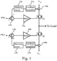
- Fig. 1 represents an example of an architecture of a half bridge configuration in which the present invention may be implemented.
- a first gate trajectory control device which is composed of a current derivative sensing means 10a, a feedback amplifier 11a, a blanking circuit 12a, a summing circuit 13a and a buffer 14a, controls the switching of a power semiconductor switch S1
- a second gate trajectory control device which is composed of a current derivative sensing means 10b, a feedback amplifier 11b, a blanking circuit 12b, a summing circuit 13b and a buffer 14b, controls the switching of a power semiconductor switch S2.
- the present invention is disclosed in an example based on an MOSFET application but can be extended to any unipolar (JFET, IGFET, HEMT) or bipolar transistor (BJT or IGBT), only the name of the electrodes needs to be changed.
- the present invention performs the switching of a power MOSFETs in two steps.
- a first step during the voltage transition, the control of the gate-source voltages is only performed by classical input signals, i.e. a square wave signals. These signals are named PW1 and PW2.
- PW1 and PW2 signals are named PW1 and PW2.
- the usage of only PW1 and PW2 signals during the voltage transition helps reducing the switching losses by having a fast transition.
- two different operations modes take place depending on the power semiconductor switch S1 or S2 function.
- One mode operates on the conducting power semiconductor switch.
- the gate-source voltage of the conducting power semiconductor switch is controlled by the combination of the signal PW1 or PW2 and the amplified feedback signal provided by the feedback amplifier 11.
- a positive current slope in the conducting power semiconductor switch generates a negative voltage at the feedback amplifier output.
- the resulting signal controls the current derivative and therefore limits the overvoltage after the transition.
- the other mode is intended for passive device like a MOSFET used in synchronous rectification and its anti-parallel diode.
- the gate to source voltage is pulled down to the negative power rail by the signal PW1 or PW2. Only the feedback signal is able to modify the gate to source voltage.
- the feedback signal is used to damp the resonant oscillations by partially saturating the power semiconductor switch.
- the power semiconductor switch acts like a variable resistor absorbing the energy stored in the parasitic elements. This energy is considered small compared to the total switching energy, while the reduced ringing improves drastically the electromagnetic perturbation.
- the reference signal PW1 is provided to the summation module 13a.
- the output of the summation module 13a is provided to the buffer 14a and the output of the buffer 14a is provided to the gate of the power semiconductor switch S1.
- the drain of the power semiconductor switch S1 is connected to a positive power supply of a bus and the current going throught the connection is sensed by the current derivative sensing means 10a.
- the outputs of the current derivative means 10a are provided to the feedback amplier 11a.
- the output of the feedback amplifier 11a is provided to the blanking circuit 12a, the output of which is provided to the summation module 13a.
- the reference signal PW2 is provided to the summation module 13b.
- the output of the summation module 13b is provided to the buffer 14b and the output of the buffer 14b is provided to the gate of the power semiconductor suwitch S2.
- the drain of the power semiconductor switch S2 is connected to the source of the power semiconductor switch S1 and to a load.
- the source of the power semiconductor switch S2 is connected to a negative power supply of the bus and the current going throught the connection is sensed by the current derivative sensing means 10b.
- the outputs of the current derivative means 10b are provided to the feedback amplier 11b.
- the output of the feedback amplifier 11b is provided to the blanking circuit 12b, the output of which is provided to the summation module 13b.
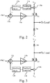
- Fig. 2 represents an example of an architecture of a buck converter in which the present invention may be implemented.
- a gate trajectory control device which is composed of a current derivative sensing means 10a, a feedback amplifier 11a, a blanking circuit 12a, a summing circuit 13a and a buffer 14a, controls the switching of a power semiconductor switch S1 that is connected to a diode Da and a load.
- the reference signal PW1 is provided to the summation module 13a.
- the output of the summation module 13a is provided to the buffer 14a and the output of the buffer 14a is provided to the gate of the power semiconductor switch S1.
- the drain of the power semiconductor switch S1 is connected to a positive power supply of the bus and the current going through the connection is sensed by the current derivative sensing means 10a.
- the source of the power semiconductor switch S1 is connected to a cathode of the diode Da, the anode of which is connected to a negative power supply.
- the outputs of the current derivative means 10a are provided to the feedback amplier 11a.
- the output of the feedback amplifier 11a is provided to the blanking circuit 12a, the output of which is provided to the summation module 13a.
- Fig. 3 represents an example of an architecture of a boost converter in which the present invention may be implemented.
- a gate trajectory control device which is composed of a current derivative sensing means 10b, a feedback amplifier 11b, a blanking circuit 12b, a summing circuit 13b and a buffer 14b, controls the switching of a power semiconductor switch S2 that is connected to a diode Db and a load.
- the reference signal PW2 is provided to the summation module 13b.
- the output of the summation module 13b is provided to the buffer 14b and the output of the buffer 14b is provided to the gate of the power semiconductor suwitch S2.
- the drain of the power semiconductor switch S2 is connected to an anode of the diode and to a load the cathode of wich is connected to a positive power supply.
- the source of the power semiconductor switch S2 is connected to a negative power supply of the bus and the current going through the connection is sensed by the current derivative sensing means 10b.
- the outputs of the current derivative means 10b are provided to the feedback amplier 11b.
- the output of the feedback amplifier 11b is provided to the blanking circuit 12b, the output of which is provided to the summation module 13b.
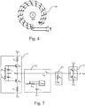
- Fig. 4 represents an example of a current derivative sensor used in the present invention.
- the current derivative sensor is, in the example of Fig. 4 , a Rogowski coil.
- a Rogowski coil is an electrical device for measuring high-speed current pulses. It consists of a helical coil of wire with the lead from one end returning through the centre of the coil to the other end, so that both terminals are at the same end of the coil. The whole assembly is then wrapped around the straight conductor whose current derivative is to be measured. There is no magnetic material core. The winding density, the diameter of the coil and the rigidity of the winding are critical for preserving immunity to external fields and sensitivity to the positioning of the measured conductor.
- Fig. 5 represents a first example of an electronic circuit of the gate trajectory control device according to the present invention.
- the feedback amplifier 11 is composed of two transistors Q 51 and Q 52 connected in a push-pull configuration, four resistors R 51 to R 54 and two capacitors C 51 and C 52 .
- a first output A of the Rogowski coil 10 is connected to first terminals of capacitors C 51 and C 52 and resistors R 53 and R 54 .
- a second output B of the Rogowski coil 10 is connected to emitters of transistors Q 51 and Q 52 .
- the transistor Q 51 is a NPN transistor and the transistor Q 52 is a PNP transistor.
- the second terminals of resistor R 53 and capacitor C 51 are connected to the base of transistor Q 51 .
- the second terminals of resistor R 54 and capacitor C 52 are connected to the base of transistor Q 52 .
- the collector of transistor Q 51 is connected to a first terminal of resistor R 51 , the second terminal of which is connected to a positive power supply Vcc.
- the collector of transistor Q 52 is connected to a first terminal of resistor R 52 , the second terminal of which is connected to a negative power supply Vee.
- the emitters of transistors Q 51 and Q 52 are the output of the feedback amplifier 11.
- the output of the feedback amplifier 11 is connected to the input of the blanking circuit 12.
- the blanking circuit 12 is composed of a resistor R 56 , a capacitor C 53 , a logic Xor gate and a switch S 50 .
- a first terminal of the switch S 50 is connected to the input of the blanking circuit 12 and a second terminal of the switch S 50 is connected to the output of the blanking circuit 12.
- the switch S 50 is controlled through the output of the Xor gate.
- An optional buffer stage may be added if the logic gate is not powerful enough to directly control the switch S 50 .
- a first input of the Xor gate is connected to the reference signal PW.
- the reference signal PW is applied to a first terminal of the resistor R 56 .
- the second terminal of the resistor R 56 is connected to a second input of the Xor gate and to a first terminal of the capacitor C 53 .
- a second terminal of the capacitor C 53 is connected to the negative power supply Vee.
- the capacitor C 53 and the resistor R 56 form a delay that is for example equal to the sum of the gate transition delay, the voltage transition time and the current transition time plus a predetermined margin.
- the output of the blanking circuit 12 is connected to the input of the summation module 13 that is composed of a resistor R 55 .
- a first terminal of the resistor R 55 is connected to the the input of the summation module 13 and a second terminal of resistor R 55 is connected to the reference signal PW.
- the output of the summation module 13 is connected to the input of the buffer 14 that is composed of two transistors Q 53 and Q 54 .
- the input of the buffer 14 is connected to the base of transistors Q 53 and Q 54 .
- the transistor Q 53 is a NPN transistor and the transistor Q 54 is a PNP transistor.
- the collector of transistor Q 53 is connected to the positive power supply Vcc.
- the collector of transistor Q 54 is connected to the negative power supply Vee.
- the emitters of transistors Q 51 and Q 52 are the output of the buffer 14.
- the output of the buffer 14 is connected to gate of power semiconductor switch S1 or S2.
- Fig. 6 represents an example of an electronic circuit of the feedback amplifier of the gate trajectory control device according to the present invention.
- the feedback amplifier 11 is composed of two transistors Q 61 and Q 62 , nine resistors R 61 to R 69 and five capacitors C 61 and C 65 .
- a first output A of the Rogowski coil 10 is connected to first terminals of capacitors C 61 and C C2 and resistors R 63 and R 64 .
- a second output B of the Rogowski coil 10 is connected to first terminals of resistors R 66 , R 67 and R 69 and of capacitors C 63 , C 64 and C 65 .
- the second terminals of transistor R 63 and capacitor C 61 are connected to a first terminal of resistor R 65 and to the base of transistor Q 61 .
- the transistor Q 61 is a NPN transistor and the transistor Q 62 is a PNP transistor.
- the second terminals of resistor R 63 and capacitor C 61 are connected to the base of transistor Q 51 and to a first terminal of resistor R 65 .
- a second terminal of resistor R 65 is connected to the positive power supply Vcc.
- the second terminals of resistor R 64 and capacitor C 62 are connected to the base of transistor Q 62 .
- the second terminals of resistor R 64 and capacitor C 62 are connected to the base of transistor Q 62 and to a first terminal of resistor R 68 .
- a second terminal of resistor R 68 is connected to the negative power supply Veec.
- the collector of transistor Q 61 is connected to a first terminal of resistor R 61 , the second terminal of which is connected to the positive power supply Vcc.
- the collector of transistor Q 62 is connected to a first terminal of resistor R 62 , the second terminal of which is connected to the negative power supply Vee.
- the second terminals of the resistor R69 and the capacitor C65 are the output of the feedback amplifier 11.
- Figs. 7a and 7b represent chronograms of signals provided according to the present invention.
- Figs 7a and 7b show the evolution in the time of the drain to source voltage VDSsi of the power semiconductor switch S1, of the drain to source voltage VDS S2 of the power semiconductor switch S2, of the drain to source current IDsi of the power semiconductor switch S1, of the drain to source current ID S2 of the power semiconductor switch S2, of the reference signals PW1 and PW2, of the gate to source voltage VGSsi of the power semiconductor switch S1, of the gate to source voltage VGS S2 of the power semiconductor switch S2, of the output 12aOut of the blanking circuit 12a, of the output 12bOut of the blanking circuit 12b, of the output 10aOut of the current derivative sensing means 10a and of the output 10bOut of the current derivative sensing means 10b.
- the reference signal PW2 is at high level and the reference signal PW1 is at low state.
- the drain to source voltage VDSsi of the power semiconductor switch S1 is equal to the bus voltage Vbus i.e.
- the drain to source voltage VDS S2 of the power semiconductor switch S2 is null
- the drain to source current IDsi of the power semiconductor switch S1 is null
- the drain to source current ID S2 of the power semiconductor switch S2 is equal to I 0
- the current supplied to the load the gate to source voltage VGSsi of the power semiconductor switch S1 is at the negative rail voltage V ee
- the gate to source voltage VGS S2 of the power semiconductor switch S2 is at high level (Vcc)
- the output 12aOut of the blanking circuit 12a is null
- the output 12bOut of the blanking circuit 12b is null
- the output 10aOut of the current derivative sensing means 10a is null
- the output 10bOut of the current derivative sensing means 10b is null.
- the reference signal PW2 moves from high state to low state and the output of the blanking circuit 12bOut moves from low state to high state.
- the drain to source voltage VDSsi of the power semiconductor switch S1 is equal to the bus voltage Vbus, the drain to source voltage VDS S2 of the power semiconductor switch S2 is null, the drain to source current IDsi of the power semiconductor switch S1 is null, the drain to source current ID S2 of the power semiconductor switch S2 is equal to I 0 , the gate to source voltage VGSsi of the power semiconductor switch S1 is null, the gate to source voltage VGS S2 of the power semiconductor switch S2 is null, the output 12aOut of the blanking circuit 12a is null, the output 10aOut of the current derivative sensing means 10a is null and the output 10bOut of the current derivative sensing means 10b is null.
- the drain to source voltage VDSsi of the power semiconductor switch S1 is equal to the bus voltage minus the voltage drop in parasitic inductances, the drain to source voltage VDS S2 of the power semiconductor switch S2 is null, the drain to source current IDsi of the power semiconductor switch S1 starts to increase, the drain to source current ID S2 of the power semiconductor switch S2 starts to decrease, the gate to source voltage VGS S1 of the power semiconductor switch S1 increases up to the Miller Plateau voltage if the power semiconductor switch has a gate or increases up to a voltage ensuring the target current derivative in the di/dt in the power semiconductor switch , the gate to source voltage VGS S2 of the power semiconductor switch S2 is null, the output 12aOut of the blanking circuit 12a is high as the output of the blanking circuit 12b, the output 10aOut of the current derivative sensing means 10a is negative and the output 10bOut of the current derivative sensing means 10b is negative.
- the reference signal PW1 and the signal 12aOut at the output of the blanking circuit 12a are at high state.
- the drain to source voltage VDSsi of the power semiconductor switch S1 is equal to the bus voltage minus the voltage drop in parastic inductances, the drain to source voltage VDS S2 of the power semiconductor switch S2 is null, the drain to source current IDsi of the power semiconductor switch S1 stops to increase, the drain to source current ID S2 of the power semiconductor switch S2 stops to decrease, the gate to source voltage VGSsi of the power semiconductor switch S1 is rising toward the positive power supply voltage V cc , the gate to source voltage VGS S2 of the power semiconductor switch S2 is null, the output 12aOut of the blanking circuit 12a is high as the output of the blanking circuit 12b, the output 10aOut of the current derivative sensing means 10a is positive and the output 10bOut of the current derivative sensing means 10b is positive.
- the current going through the power semiconductor switch S1 has reached the output current plus the recovery current of the anti-parrallel diode of the power semiconductor switch S2.
- the current is falling back to the output current leading to a positive feedback voltage added to the already positive reference signal.
- the gate voltage of the power semiconductor switch S1 is pulled up to the positive power supply voltage.
- the feedback voltage is also positive; this voltage is added to the pulled down reference signal PW2 leading to a positive voltage on the power semiconductor switch S2 gate.
- Both power semiconductor switches S1 and S2 are in a linear state.
- the power semiconductor switch can be modelled as a variable resistor damping the oscillating circuit made by the parasitic inductance and capacitance.
- the anti-parallel diode of the power semiconductor switch S2 is blocked at time t 2 enabling the voltage fall on the power semiconductor switch S1 and conversely the rise on the power semiconductor switch S1.
- the voltage across the power semiconductor switch S2 has reached the bus voltage V bus . Consequently the voltage across the power semiconductor switch S1 is null. No current is flowing in the power semiconductor switch S2 and all the load current I 0 is flowing in the power semiconductor switch S1.
- the gate to source voltage VGSsi of the power semiconductor switch S1 has reached the positive supplied voltage V cc .
- the gate to source voltage VGS S2 of the power semiconductor switch S2 is pulled down to the negative supply voltage V ee by the signal PW2.
- the output 10bOut of the current derivative sensing means 10b is null. As a result, no feedback is added to PW2.
- the turn-off phase starts at time t 4 .
- the reference signal PW1 moves from high state to low state and the output of the blanking circuit 12aOut moves from low state to high state.
- the gate of the power semiconductor switch S1 is pulled down to the negative power supply V ee .
- the gate to source of the power semiconductor switch S1 is falling towards the negative power supply V ee . All the other signals remain identical until the gate to source voltage of the power semiconductor switch S1 has reached the Miller plateau voltage.
- the current starts falling and a feedback compensation is added to the reference signal PW1 of power semiconductor switch S1 slowing down the current transition.
- the blanking circuit is preventing the feedback on the power semiconductor switch S2 to turn on the power semiconductor switch S2 leading to a leg short-circuit. Since PW2 signal provided to the power semiconductor switch S2 is at low level, the output 12aOut of the blanking circuit 12a stays low during all the turn-off phase. The gate to source voltage VGS S2 of the power semiconductor switch S2 is pulled down to the negative supply voltage.
- the voltage across the power semiconductor switch S2 is null and the voltage across the power semiconductor switch S1 is equal to the bus voltage V bus .
- the current can start to fall in the power semiconductor switch S2 and consequently rises in the power semiconductor switch S1.
- This step current slope induces a positive voltage at the output 10bOut of the current derivative sensing means 10.
- This voltage is added to the negative voltage of the reference signal PW2. Therefore the gate to source voltage VGSsi of the power semiconductor switch S1 increases up to a voltage ensuring the target di/dt in the power semiconductor switch S1.
- the current slope in the switch is regulated by the feedback loop.
- the current in the power semiconductor switch S1 is null and the current in the power semiconductor switch S2 has reached the load current I 0 .
- the output 10bOut of the current derivative sensing means 10 is null.
- the gate to source voltage VGSsi of the power semiconductor switch S is pulled down to the negative power supply Vss of the bus.
- Fig. 8 represents a detailed chronogram of current and voltages on a power semiconductor switch during switching OFF when the present invention is or is not implemented.
- VDSS' shows the drain to source voltage of a power semiconductor switch during switching OFF when the present invention is not implemented and the curve noted VDSS shows the drain to source voltage of a power semiconductor switch during switching OFF when the present invention is implemented.
- the curve noted IDS' shows the drain to source current of a power semiconductor switch during switching OFF when the present invention is not implemented and the curve noted IDS shows the drain to source current of a power semiconductor switch during switching OFF when the present invention is implemented.
- the curve noted VGSS' shows the gate to source voltage of a power semiconductor switch during switching OFF when the present invention is not implemented and the curve noted VGSS shows the drain to source voltage of a power semiconductor switch during switching OFF when the present invention is implemented.
- the present invention reduces the current transient rate and/or the voltage overshoot.
- Fig. 9 represents a detailed chronogram of current and voltages on a power semiconductor switch during switching ON when the present invention is or is not implemented.
- VDSS' shows the drain to source voltage of a power semiconductor switch during switching ON when the present invention is not implemented and the curve noted VDSS shows the drain to source voltage of a power semiconductor switch during switching ON when the present invention is implemented.
- the curve noted IDS' shows the drain to source current of a power semiconductor switch during switching ON when the present invention is not implemented and the curve noted IDS shows the drain to source current of a power semiconductor switch during switching ON when the present invention is implemented.
- the curve noted VGSS' shows the gate to source voltage of a power semiconductor switch during switching ON when the present invention is not implemented and the curve noted VGSS shows the drain to source voltage of a power semiconductor switch during switching ON when the present invention is implemented.
- the present invention reduces the current transient rate and/or the voltage overshoot.
- Fig. 10 represents a second example of an architecture of a gate trajectory control device according to the present invention.
- the gate trajectory control device has, for example, an architecture based on components connected together by a bus 101 and a processor 100 controlled by a program as disclosed in Fig. 11 .
- the bus 101 links the processor 100 to a read only memory ROM 102, a random access memory RAM 103 and an input output I/O IF interface 105.
- the memory 103 contains registers intended to receive variables and the instructions of the program related to the algorithm as disclosed in Fig. 11 .
- the processor 100 receives through the input output I/O IF 105 measurement of the derivative of the drain to source current, the input signal PW1 or PW2.
- the read-only memory, or possibly a Flash memory 102 contains instructions of the program related to the algorithm as disclosed in Fig. 11 , when the reference module 102 is powered on, to the random access memory 103.
- the gate trajectory control device may be implemented in software by execution of a set of instructions or program by a programmable computing machine, such as a PC ( Personal Computer ), a DSP ( Digital Signal Processor ) or a microcontroller; or else implemented in hardware by a machine or a dedicated component, such as an FPGA ( Field-Programmable Gate Array ) or an ASIC ( Application-Specific Integrated Circuit).
- a programmable computing machine such as a PC ( Personal Computer ), a DSP ( Digital Signal Processor ) or a microcontroller; or else implemented in hardware by a machine or a dedicated component, such as an FPGA ( Field-Programmable Gate Array ) or an ASIC ( Application-Specific Integrated Circuit).
- the gate trajectory control device includes circuitry, or a device including circuitry, causing the gate trajectory control device to perform the program related to the algorithm as disclosed in Fig. 11 .
- Fig. 11 represents an algorithm executed by the gate trajectory control device according to the second example of gate trajectory control device.
- the gate trajectory control device receives an input signal that is intended to drive the semiconductor power switch, characterized in that the device comprises:
Landscapes
- Engineering & Computer Science (AREA)
- Power Engineering (AREA)
- Electronic Switches (AREA)
- Dc-Dc Converters (AREA)
- Power Conversion In General (AREA)
Abstract
Description
- The present invention relates generally to a device and a method for controlling the switching of at least a first power semiconductor switch providing current to a load.
- A classical gate driver circuit contains fixed positive and negative voltage/current power supplies called Vcc for the positive voltage and Vee for the negative one, both referenced to the source of the semiconductor switch. Depending on the desired state of the semiconductor switch, the power semiconductor switch gate is connected to either supply rail by means of a switch and an optional gate resistance. For turning-on the semiconductor switch, the positive voltage/current source is connected to the gate control of the semiconductor switch, for turning-off the semiconductor switch the negative voltage/current source is connected to the gate control of the device.
- Today, the switching frequency of power converters is increasing. Wide-band gap devices like GaN and SiC devices provide faster switching capabilities than classical technologies.
- Wide band gap power semiconductor devices are able to switch at a high speed like for example superior to 10V/ns. This reduces the switching losses, and thus allows the use of higher switching frequencies.
- High switching speed may create voltage overshoots between drain and source of power semiconductor transistor for example due to the layout stray inductance increasing the switching losses and over stressing the transistor. Overshoot may also create conducted and radiated EMI.
- Some techniques applied to the gate driver circuit are used to reduce the switching speed (the voltage and current transient rate) and/or the voltage overshoot, and ringing.
- The passive techniques consist in basically changing the power semiconductor switch switching behavior by inserting passive components, changing the external gate resistance and the voltage/current source values. These techniques may be used to adjust the switching speed of the semiconductor switch. However, this permanent modification on the gate driver circuit impacts the performance of the power semiconductor switch. In addition, the switching characteristics are dependent of the operating point of the power semiconductor switch.
- The present invention aims to allow a fast switching with a low voltage overshoot and reduced ringing at the end of the switching either during turn-on and turn-off using an active controlled feedback signal that is injected in the gate driver circuit.
- To that end, the present invention concerns a device for controlling the switching from a conducting state to a non conducting state or from a non conducting state to a conducting state of a semiconductor power switch providing current to a load, the device receiving an input signal that is intended to drive the semiconductor power switch, characterized in that the device comprises:
- means for sensing the derivative of the drain to source current going through the semiconductor power switch in order to obtain a voltage representative of the sensed derivative of the drain to source current,
- means for amplifying the voltage representative of the sensed derivative of the drain to source current,
- means for adding the amplified voltage representative of the sensed derivative of the drain to source current to the input signal during a given time period.
- The present invention concerns also a method for controlling the switching from a conducting state to a non conducting state or from a non conducting state to a conducting state of a semiconductor power switch providing current to a load, characterized in that the method comprises the steps of:
- receiving an input signal that is intended to drive the semiconductor power switch, characterized in that the device comprises:
- sensing the derivative of the drain to source current going through the semiconductor power switch in order to obtain a voltage representative of the sensed derivative of the drain to source current,
- amplifying the voltage representative of the derivative of the sensed drain to source current,
- adding the amplified voltage representative of the derivative of the sensed drain to source current to the input signal during a given time period.
- Thus, the present invention reduces the current transient rate and/or the voltage overshoot.
- According to a particular feature, the means for sensing the derivative of the drain to source current going through the semiconductor power switch are composed of a Rogowski coil.
- Thus, no additional circuitry is required comparing to a current sensor that will need a derivative block. In addition, the Rogowski coil is able to measure the derivative contactless and is not dependent on the switch parasitic inductance.
- According to a particular feature, the given time period is the sum of the gate transition time, the voltage transition time and the current transition time plus a predetermined margin.
- Thus, the current sensor is controlling the semiconductor power switch only during transition avoiding any spurious shoot through during the rest of the switching period.
- According to a particular feature, the semiconductor power switch is included in a buck converter.
- According to a particular feature, the semiconductor power switch is included in a boost converter.
- According to a particular feature, the semiconductor power switch is included in a half bridge configuration that comprises a first and a second semiconductor power switches and the switching of each semiconductor power switch being controlled by a respective device for controlling the switching from a conducting state to a non conducting state or from a non conducting state to a conducting state.
- The characteristics of the invention will emerge more clearly from a reading of the following description of example embodiments, the said description being produced with reference to the accompanying drawings, among which :
-
Fig. 1 represents an example of an architecture of a half bridge configuration in which the present invention may be implemented; -
Fig. 2 represents an example of an architecture of a buck converter in which the present invention may be implemented; -
Fig. 3 represents an example of an architecture of a boost converter in which the present invention may be implemented; -
Fig. 4 represents an example of a current derivative sensor used in the present invention; -
Fig. 5 represents a first example of an electronic circuit of the gate trajectory control device according to the present invention; -
Fig. 6 represents an example of an electronic circuit of the feedback amplifier of the gate trajectory control device according to the present invention; -
Figs. 7a and7b represent chronograms of signals provided according to the present invention; -
Fig. 8 represents a detailled chronogram of current and voltages on a power semiconductor switch during switching OFF when the present invention is or is not implemented; -
Fig. 9 represents a detailled chronogram of current and voltages on a power semiconductor switch during switching ON when the present invention is or is not implemented; -
Fig. 10 represents a second example of an architecture of a gate trajectory control device according to the present invention; -
Fig. 11 represents an algorithm executed by the gate trajectory control device according to the second example of gate trajectory control device. -
Fig. 1 represents an example of an architecture of a half bridge configuration in which the present invention may be implemented. - In the example of
Fig. 1 , a first gate trajectory control device which is composed of a current derivative sensing means 10a, a feedback amplifier 11a, a blankingcircuit 12a, a summingcircuit 13a and abuffer 14a, controls the switching of a power semiconductor switch S1 and a second gate trajectory control device which is composed of a current derivative sensing means 10b, afeedback amplifier 11b, a blankingcircuit 12b, a summingcircuit 13b and abuffer 14b, controls the switching of a power semiconductor switch S2. - The present invention is disclosed in an example based on an MOSFET application but can be extended to any unipolar (JFET, IGFET, HEMT) or bipolar transistor (BJT or IGBT), only the name of the electrodes needs to be changed.
- The present invention performs the switching of a power MOSFETs in two steps. At a first step, during the voltage transition, the control of the gate-source voltages is only performed by classical input signals, i.e. a square wave signals. These signals are named PW1 and PW2. The usage of only PW1 and PW2 signals during the voltage transition helps reducing the switching losses by having a fast transition. Then, during the second step i.e. during the current transition, two different operations modes take place depending on the power semiconductor switch S1 or S2 function.
- One mode operates on the conducting power semiconductor switch. The gate-source voltage of the conducting power semiconductor switch is controlled by the combination of the signal PW1 or PW2 and the amplified feedback signal provided by the
feedback amplifier 11. A positive current slope in the conducting power semiconductor switch generates a negative voltage at the feedback amplifier output. The resulting signal controls the current derivative and therefore limits the overvoltage after the transition. - The other mode is intended for passive device like a MOSFET used in synchronous rectification and its anti-parallel diode. In this mode, the gate to source voltage is pulled down to the negative power rail by the signal PW1 or PW2. Only the feedback signal is able to modify the gate to source voltage.
- After the current transition, in both modes, the feedback signal is used to damp the resonant oscillations by partially saturating the power semiconductor switch. The power semiconductor switch acts like a variable resistor absorbing the energy stored in the parasitic elements. This energy is considered small compared to the total switching energy, while the reduced ringing improves drastically the electromagnetic perturbation.
- The reference signal PW1 is provided to the
summation module 13a. The output of thesummation module 13a is provided to thebuffer 14a and the output of thebuffer 14a is provided to the gate of the power semiconductor switch S1. - The drain of the power semiconductor switch S1 is connected to a positive power supply of a bus and the current going throught the connection is sensed by the current derivative sensing means 10a.
- The outputs of the current derivative means 10a are provided to the feedback amplier 11a. The output of the feedback amplifier 11a is provided to the
blanking circuit 12a, the output of which is provided to thesummation module 13a. - The reference signal PW2 is provided to the
summation module 13b. The output of thesummation module 13b is provided to thebuffer 14b and the output of thebuffer 14b is provided to the gate of the power semiconductor suwitch S2. - The drain of the power semiconductor switch S2 is connected to the source of the power semiconductor switch S1 and to a load.
- The source of the power semiconductor switch S2 is connected to a negative power supply of the bus and the current going throught the connection is sensed by the current derivative sensing means 10b.
- The outputs of the current derivative means 10b are provided to the
feedback amplier 11b. The output of thefeedback amplifier 11b is provided to theblanking circuit 12b, the output of which is provided to thesummation module 13b. -
Fig. 2 represents an example of an architecture of a buck converter in which the present invention may be implemented. - In the example of
Fig. 2 , a gate trajectory control device, which is composed of a current derivative sensing means 10a, a feedback amplifier 11a, a blankingcircuit 12a, a summingcircuit 13a and abuffer 14a, controls the switching of a power semiconductor switch S1 that is connected to a diode Da and a load. - The reference signal PW1 is provided to the
summation module 13a. The output of thesummation module 13a is provided to thebuffer 14a and the output of thebuffer 14a is provided to the gate of the power semiconductor switch S1. - The drain of the power semiconductor switch S1 is connected to a positive power supply of the bus and the current going through the connection is sensed by the current derivative sensing means 10a.
- The source of the power semiconductor switch S1 is connected to a cathode of the diode Da, the anode of which is connected to a negative power supply.
- The outputs of the current derivative means 10a are provided to the feedback amplier 11a. The output of the feedback amplifier 11a is provided to the
blanking circuit 12a, the output of which is provided to thesummation module 13a. -
Fig. 3 represents an example of an architecture of a boost converter in which the present invention may be implemented. - In the example of
Fig. 3 , a gate trajectory control device which is composed of a current derivative sensing means 10b, afeedback amplifier 11b, a blankingcircuit 12b, a summingcircuit 13b and abuffer 14b, controls the switching of a power semiconductor switch S2 that is connected to a diode Db and a load. - The reference signal PW2 is provided to the
summation module 13b. The output of thesummation module 13b is provided to thebuffer 14b and the output of thebuffer 14b is provided to the gate of the power semiconductor suwitch S2. - The drain of the power semiconductor switch S2 is connected to an anode of the diode and to a load the cathode of wich is connected to a positive power supply.
- The source of the power semiconductor switch S2 is connected to a negative power supply of the bus and the current going through the connection is sensed by the current derivative sensing means 10b.
- The outputs of the current derivative means 10b are provided to the
feedback amplier 11b. The output of thefeedback amplifier 11b is provided to theblanking circuit 12b, the output of which is provided to thesummation module 13b. -
Fig. 4 represents an example of a current derivative sensor used in the present invention. - The current derivative sensor is, in the example of
Fig. 4 , a Rogowski coil. A Rogowski coil is an electrical device for measuring high-speed current pulses. It consists of a helical coil of wire with the lead from one end returning through the centre of the coil to the other end, so that both terminals are at the same end of the coil. The whole assembly is then wrapped around the straight conductor whose current derivative is to be measured. There is no magnetic material core. The winding density, the diameter of the coil and the rigidity of the winding are critical for preserving immunity to external fields and sensitivity to the positioning of the measured conductor. -
Fig. 5 represents a first example of an electronic circuit of the gate trajectory control device according to the present invention. - The
feedback amplifier 11 is composed of two transistors Q51 and Q52 connected in a push-pull configuration, four resistors R51 to R54 and two capacitors C51 and C52. - A first output A of the
Rogowski coil 10 is connected to first terminals of capacitors C51 and C52 and resistors R53 and R54. - A second output B of the
Rogowski coil 10 is connected to emitters of transistors Q51 and Q52. - The transistor Q51 is a NPN transistor and the transistor Q52 is a PNP transistor.
- The second terminals of resistor R53 and capacitor C51 are connected to the base of transistor Q51.
- The second terminals of resistor R54 and capacitor C52 are connected to the base of transistor Q52.
- The collector of transistor Q51 is connected to a first terminal of resistor R51, the second terminal of which is connected to a positive power supply Vcc.
- The collector of transistor Q52 is connected to a first terminal of resistor R52, the second terminal of which is connected to a negative power supply Vee.
- The emitters of transistors Q51 and Q52 are the output of the
feedback amplifier 11. - The output of the
feedback amplifier 11 is connected to the input of the blankingcircuit 12. - The blanking
circuit 12 is composed of a resistor R56, a capacitor C53, a logic Xor gate and a switch S50. - A first terminal of the switch S50 is connected to the input of the blanking
circuit 12 and a second terminal of the switch S50 is connected to the output of the blankingcircuit 12. - The switch S50 is controlled through the output of the Xor gate. An optional buffer stage may be added if the logic gate is not powerful enough to directly control the switch S50.
- A first input of the Xor gate is connected to the reference signal PW.
- The reference signal PW is applied to a first terminal of the resistor R56.
- The second terminal of the resistor R56 is connected to a second input of the Xor gate and to a first terminal of the capacitor C53. A second terminal of the capacitor C53 is connected to the negative power supply Vee.
- The capacitor C53 and the resistor R56 form a delay that is for example equal to the sum of the gate transition delay, the voltage transition time and the current transition time plus a predetermined margin.
- The output of the blanking
circuit 12 is connected to the input of thesummation module 13 that is composed of a resistor R55. - A first terminal of the resistor R55 is connected to the the input of the
summation module 13 and a second terminal of resistor R55 is connected to the reference signal PW. - The output of the
summation module 13 is connected to the input of thebuffer 14 that is composed of two transistors Q53 and Q54. - The input of the
buffer 14 is connected to the base of transistors Q53 and Q54. - The transistor Q53 is a NPN transistor and the transistor Q54 is a PNP transistor.
- The collector of transistor Q53 is connected to the positive power supply Vcc.
- The collector of transistor Q54 is connected to the negative power supply Vee.
- The emitters of transistors Q51 and Q52 are the output of the
buffer 14. - The output of the
buffer 14 is connected to gate of power semiconductor switch S1 or S2. -
Fig. 6 represents an example of an electronic circuit of the feedback amplifier of the gate trajectory control device according to the present invention. - The
feedback amplifier 11 is composed of two transistors Q61 and Q62, nine resistors R61 to R69 and five capacitors C61 and C65. - A first output A of the
Rogowski coil 10 is connected to first terminals of capacitors C61 and CC2 and resistors R63 and R64. - A second output B of the
Rogowski coil 10 is connected to first terminals of resistors R66, R67 and R69 and of capacitors C63, C64 and C65. - The second terminals of transistor R63 and capacitor C61 are connected to a first terminal of resistor R65 and to the base of transistor Q61.
- The transistor Q61 is a NPN transistor and the transistor Q62 is a PNP transistor.
- The second terminals of resistor R63 and capacitor C61 are connected to the base of transistor Q51 and to a first terminal of resistor R65.
- A second terminal of resistor R65 is connected to the positive power supply Vcc.
- The second terminals of resistor R64 and capacitor C62 are connected to the base of transistor Q62.
- The second terminals of resistor R64 and capacitor C62 are connected to the base of transistor Q62 and to a first terminal of resistor R68.
- A second terminal of resistor R68 is connected to the negative power supply Veec.
- The collector of transistor Q61 is connected to a first terminal of resistor R61, the second terminal of which is connected to the positive power supply Vcc.
- The collector of transistor Q62 is connected to a first terminal of resistor R62, the second terminal of which is connected to the negative power supply Vee.
- The second terminals of the resistor R69 and the capacitor C65 are the output of the
feedback amplifier 11. -
Figs. 7a and7b represent chronograms of signals provided according to the present invention. - The
Figs 7a and7b show the evolution in the time of the drain to source voltage VDSsi of the power semiconductor switch S1, of the drain to source voltage VDSS2 of the power semiconductor switch S2, of the drain to source current IDsi of the power semiconductor switch S1, of the drain to source current IDS2 of the power semiconductor switch S2, of the reference signals PW1 and PW2, of the gate to source voltage VGSsi of the power semiconductor switch S1, of the gate to source voltage VGSS2 of the power semiconductor switch S2, of the output 12aOut of the blankingcircuit 12a, of the output 12bOut of the blankingcircuit 12b, of the output 10aOut of the current derivative sensing means 10a and of the output 10bOut of the current derivative sensing means 10b. - Before time to of
Figs. 7 , the reference signal PW2 is at high level and the reference signal PW1 is at low state. Before time to, the drain to source voltage VDSsi of the power semiconductor switch S1 is equal to the bus voltage Vbus i.e. the sum of absolute values of the positive and negative power suplies of the bus VDD and Vss, the drain to source voltage VDSS2 of the power semiconductor switch S2 is null, the drain to source current IDsi of the power semiconductor switch S1 is null, the drain to source current IDS2 of the power semiconductor switch S2 is equal to I0, the current supplied to the load, the gate to source voltage VGSsi of the power semiconductor switch S1 is at the negative rail voltage Vee, the gate to source voltage VGSS2 of the power semiconductor switch S2 is at high level (Vcc), the output 12aOut of the blankingcircuit 12a is null, the output 12bOut of the blankingcircuit 12b is null, the output 10aOut of the current derivative sensing means 10a is null and the output 10bOut of the current derivative sensing means 10b is null. - At time to, the reference signal PW2 moves from high state to low state and the output of the blanking circuit 12bOut moves from low state to high state.
- The drain to source voltage VDSsi of the power semiconductor switch S1 is equal to the bus voltage Vbus, the drain to source voltage VDSS2 of the power semiconductor switch S2 is null, the drain to source current IDsi of the power semiconductor switch S1 is null, the drain to source current IDS2 of the power semiconductor switch S2 is equal to I0, the gate to source voltage VGSsi of the power semiconductor switch S1 is null, the gate to source voltage VGSS2 of the power semiconductor switch S2 is null, the output 12aOut of the blanking
circuit 12a is null, the output 10aOut of the current derivative sensing means 10a is null and the output 10bOut of the current derivative sensing means 10b is null. - At time t1, the reference signal PW1 and the signal 12aOut at the output of the blanking
circuit 12a move to high state. - The drain to source voltage VDSsi of the power semiconductor switch S1 is equal to the bus voltage minus the voltage drop in parasitic inductances, the drain to source voltage VDSS2 of the power semiconductor switch S2 is null, the drain to source current IDsi of the power semiconductor switch S1 starts to increase, the drain to source current IDS2 of the power semiconductor switch S2 starts to decrease, the gate to source voltage VGSS1 of the power semiconductor switch S1 increases up to the Miller Plateau voltage if the power semiconductor switch has a gate or increases up to a voltage ensuring the target current derivative in the di/dt in the power semiconductor switch , the gate to source voltage VGSS2 of the power semiconductor switch S2 is null, the output 12aOut of the blanking
circuit 12a is high as the output of the blankingcircuit 12b, the output 10aOut of the current derivative sensing means 10a is negative and the output 10bOut of the current derivative sensing means 10b is negative. - At time t2, the reference signal PW1 and the signal 12aOut at the output of the blanking
circuit 12a are at high state. - The drain to source voltage VDSsi of the power semiconductor switch S1 is equal to the bus voltage minus the voltage drop in parastic inductances, the drain to source voltage VDSS2 of the power semiconductor switch S2 is null, the drain to source current IDsi of the power semiconductor switch S1 stops to increase, the drain to source current IDS2 of the power semiconductor switch S2 stops to decrease, the gate to source voltage VGSsi of the power semiconductor switch S1 is rising toward the positive power supply voltage Vcc, the gate to source voltage VGSS2 of the power semiconductor switch S2 is null, the output 12aOut of the blanking
circuit 12a is high as the output of the blankingcircuit 12b, the output 10aOut of the current derivative sensing means 10a is positive and the output 10bOut of the current derivative sensing means 10b is positive. - At time t2, the current going through the power semiconductor switch S1 has reached the output current plus the recovery current of the anti-parrallel diode of the power semiconductor switch S2. The current is falling back to the output current leading to a positive feedback voltage added to the already positive reference signal. Thus, the gate voltage of the power semiconductor switch S1 is pulled up to the positive power supply voltage. On the power semiconductor switch S2, the feedback voltage is also positive; this voltage is added to the pulled down reference signal PW2 leading to a positive voltage on the power semiconductor switch S2 gate. Both power semiconductor switches S1 and S2 are in a linear state. In this case, the power semiconductor switch can be modelled as a variable resistor damping the oscillating circuit made by the parasitic inductance and capacitance. The anti-parallel diode of the power semiconductor switch S2 is blocked at time t2 enabling the voltage fall on the power semiconductor switch S1 and conversely the rise on the power semiconductor switch S1.
- At time t3, the voltage across the power semiconductor switch S2 has reached the bus voltage Vbus. Consequently the voltage across the power semiconductor switch S1 is null. No current is flowing in the power semiconductor switch S2 and all the load current I0 is flowing in the power semiconductor switch S1. The gate to source voltage VGSsi of the power semiconductor switch S1 has reached the positive supplied voltage Vcc. The gate to source voltage VGSS2 of the power semiconductor switch S2 is pulled down to the negative supply voltage Vee by the signal PW2. The output 10bOut of the current derivative sensing means 10b is null. As a result, no feedback is added to PW2. On the power semiconductor switch S2, there is an overshoot voltage that is directly related to the current slope in the power semiconductor switch just before time t3. The value of this current slope is proportional to the current slope controlled by the power semiconductor switch S1 during the interval between t1 and t2.
- The turn-off phase starts at time t4. At this time, the reference signal PW1 moves from high state to low state and the output of the blanking circuit 12aOut moves from low state to high state. The gate of the power semiconductor switch S1 is pulled down to the negative power supply Vee. The gate to source of the power semiconductor switch S1 is falling towards the negative power supply Vee. All the other signals remain identical until the gate to source voltage of the power semiconductor switch S1 has reached the Miller plateau voltage.
- At time t5, the voltage rises across the power semiconductor switch S1 without any feedback compensation. The opposite voltage transition occurs on the power semiconductor switch S2. This voltage variation induces a current in the power semiconductor switch capacitance:

- Then, at time t6, the current starts falling and a feedback compensation is added to the reference signal PW1 of power semiconductor switch S1 slowing down the current transition. In the mean time, the blanking circuit is preventing the feedback on the power semiconductor switch S2 to turn on the power semiconductor switch S2 leading to a leg short-circuit. Since PW2 signal provided to the power semiconductor switch S2 is at low level, the output 12aOut of the blanking
circuit 12a stays low during all the turn-off phase. The gate to source voltage VGSS2 of the power semiconductor switch S2 is pulled down to the negative supply voltage. - At time t6, the voltage across the power semiconductor switch S2 is null and the voltage across the power semiconductor switch S1 is equal to the bus voltage Vbus. At this time, the current can start to fall in the power semiconductor switch S2 and consequently rises in the power semiconductor switch S1. This step current slope induces a positive voltage at the output 10bOut of the current derivative sensing means 10. This voltage is added to the negative voltage of the reference signal PW2. Therefore the gate to source voltage VGSsi of the power semiconductor switch S1 increases up to a voltage ensuring the target di/dt in the power semiconductor switch S1. During this time interval, the current slope in the switch is regulated by the feedback loop.
- Between intervals t6 and t7, there is an overvoltage on the power semiconductor switch S1. This overvoltage is determined by the current slope in the power semiconductor switch during the aforementioned interval.
- At t7, the current in the power semiconductor switch S1 is null and the current in the power semiconductor switch S2 has reached the load current I0. The output 10bOut of the current derivative sensing means 10 is null. The gate to source voltage VGSsi of the power semiconductor switch S is pulled down to the negative power supply Vss of the bus.
-
Fig. 8 represents a detailed chronogram of current and voltages on a power semiconductor switch during switching OFF when the present invention is or is not implemented. - The curve noted VDSS' shows the drain to source voltage of a power semiconductor switch during switching OFF when the present invention is not implemented and the curve noted VDSS shows the drain to source voltage of a power semiconductor switch during switching OFF when the present invention is implemented.
- The curve noted IDS' shows the drain to source current of a power semiconductor switch during switching OFF when the present invention is not implemented and the curve noted IDS shows the drain to source current of a power semiconductor switch during switching OFF when the present invention is implemented.
- The curve noted VGSS' shows the gate to source voltage of a power semiconductor switch during switching OFF when the present invention is not implemented and the curve noted VGSS shows the drain to source voltage of a power semiconductor switch during switching OFF when the present invention is implemented.
- As it can be seen in
Fig. 8 , the present invention reduces the current transient rate and/or the voltage overshoot. -
Fig. 9 represents a detailed chronogram of current and voltages on a power semiconductor switch during switching ON when the present invention is or is not implemented. - The curve noted VDSS' shows the drain to source voltage of a power semiconductor switch during switching ON when the present invention is not implemented and the curve noted VDSS shows the drain to source voltage of a power semiconductor switch during switching ON when the present invention is implemented.
- The curve noted IDS' shows the drain to source current of a power semiconductor switch during switching ON when the present invention is not implemented and the curve noted IDS shows the drain to source current of a power semiconductor switch during switching ON when the present invention is implemented.
- The curve noted VGSS' shows the gate to source voltage of a power semiconductor switch during switching ON when the present invention is not implemented and the curve noted VGSS shows the drain to source voltage of a power semiconductor switch during switching ON when the present invention is implemented.
- As it can be seen in
Fig. 9 , the present invention reduces the current transient rate and/or the voltage overshoot. -
Fig. 10 represents a second example of an architecture of a gate trajectory control device according to the present invention. - The gate trajectory control device has, for example, an architecture based on components connected together by a
bus 101 and aprocessor 100 controlled by a program as disclosed inFig. 11 . - The
bus 101 links theprocessor 100 to a read onlymemory ROM 102, a randomaccess memory RAM 103 and an input output I/O IF interface 105. - The
memory 103 contains registers intended to receive variables and the instructions of the program related to the algorithm as disclosed inFig. 11 . - The
processor 100 receives through the input output I/O IF 105 measurement of the derivative of the drain to source current, the input signal PW1 or PW2. - The read-only memory, or possibly a
Flash memory 102 contains instructions of the program related to the algorithm as disclosed inFig. 11 , when thereference module 102 is powered on, to therandom access memory 103. - The gate trajectory control device may be implemented in software by execution of a set of instructions or program by a programmable computing machine, such as a PC (Personal Computer), a DSP (Digital Signal Processor) or a microcontroller; or else implemented in hardware by a machine or a dedicated component, such as an FPGA (Field-Programmable Gate Array) or an ASIC (Application-Specific Integrated Circuit).
- In other words, the gate trajectory control device includes circuitry, or a device including circuitry, causing the gate trajectory control device to perform the program related to the algorithm as disclosed in
Fig. 11 . -
Fig. 11 represents an algorithm executed by the gate trajectory control device according to the second example of gate trajectory control device. - At step S110, the gate trajectory control device receives an input signal that is intended to drive the semiconductor power switch, characterized in that the device comprises:
- At step S111, the gate trajectory control device senses the drain to source current going through the semiconductor power switch in order to obtain a voltage representative of the sensed drain to source current,
- At step S112, the gate trajectory control device amplifies the voltage representative of the sensed drain to source current,
- At step S113, the gate trajectory control device adds the amplified voltage representative of the sensed drain to source current to the input signal during a given time period.
- Naturally, many modifications can be made to the embodiments of the invention described above without departing from the scope of the present invention.
Claims (9)
- Device for controlling the switching from a conducting state to a non conducting state or from a non conducting state to a conducting state of a semiconductor power switch providing current to a load, the device receiving an input signal that is intended to drive the semiconductor power switch, characterized in that the device comprises:- means for sensing the derivative of the drain to source current going through the semiconductor power switch in order to obtain a voltage representative of the sensed derivative of drain to source current,- means for amplifying the voltage representative of the sensed derivative of drain to source current,- means for adding the amplified voltage representative of the derivative of the sensed drain to source current to the input signal during a given time period.
- The device according to claim 1, characterized in that the means for sensing the derivative of the drain to source current going through the semiconductor power switch are composed of a Rogowski coil.
- The device according to claim 1 or 2, characterized in that the given time period is the sum of the gate transition time, the voltage transition time and the current transition time plus a predetermined margin.
- The device according to any of the claims 1 or 3, characterized in that the semiconductor power switch is included in a buck converter.
- The device according to any of the claims 1 or 3, characterized in that the semiconductor power switch is included in a boost converter.
- The device according to any of the claims 1 or 3, characterized in that the semiconductor power switch is included in a half bridge configuration that comprises a first and a second semiconductor power switches and the switching of each semiconductor power switch being controlled by a respective device for controlling the switching from a conducting state to a non conducting state or from a non conducting state to a conducting state.
- A method for controlling the switching from a conducting state to a non conducting state or from a non conducting state to a conducting state of a semiconductor power switch providing current to a load, characterized in that the method comprises the steps of:- receiving an input signal that is intended to drive the semiconductor power switch, characterized in that the device comprises:- sensing the derivative of the drain to source current going through the semiconductor power switch in order to obtain a voltage representative of the sensed the derivative of drain to source current,- amplifying the voltage representative of the sensed derivative of the drain to source current,- adding the amplified voltage representative of the sensed derivative of the drain to source current to the input signal during a given time period.
- The method according to claim 6, characterized in that the sensing derivative of the drain to source current going through the semiconductor power switch is performed using a Rogowski coil.
- The device according to claim 6 or 7, characterized in that the given time period is the sum of the gate transition time, the voltage transition time and the current transition time plus a predetermined margin.
Priority Applications (5)
| Application Number | Priority Date | Filing Date | Title |
|---|---|---|---|
| EP18163864.4A EP3547538B1 (en) | 2018-03-26 | 2018-03-26 | A device and a method for controlling the switching of at least a first power semiconductor switch |
| US16/975,947 US11038498B2 (en) | 2018-03-26 | 2019-03-06 | Device and method for controlling switching |
| CN201980020758.2A CN111937308B (en) | 2018-03-26 | 2019-03-06 | Device and method for controlling switching |
| JP2020537022A JP6952903B2 (en) | 2018-03-26 | 2019-03-06 | Devices and methods to control switching |
| PCT/JP2019/010125 WO2019188267A1 (en) | 2018-03-26 | 2019-03-06 | Device and method for controlling switching |
Applications Claiming Priority (1)
| Application Number | Priority Date | Filing Date | Title |
|---|---|---|---|
| EP18163864.4A EP3547538B1 (en) | 2018-03-26 | 2018-03-26 | A device and a method for controlling the switching of at least a first power semiconductor switch |
Publications (2)
| Publication Number | Publication Date |
|---|---|
| EP3547538A1 true EP3547538A1 (en) | 2019-10-02 |
| EP3547538B1 EP3547538B1 (en) | 2021-08-11 |
Family
ID=61801866
Family Applications (1)
| Application Number | Title | Priority Date | Filing Date |
|---|---|---|---|
| EP18163864.4A Active EP3547538B1 (en) | 2018-03-26 | 2018-03-26 | A device and a method for controlling the switching of at least a first power semiconductor switch |
Country Status (5)
| Country | Link |
|---|---|
| US (1) | US11038498B2 (en) |
| EP (1) | EP3547538B1 (en) |
| JP (1) | JP6952903B2 (en) |
| CN (1) | CN111937308B (en) |
| WO (1) | WO2019188267A1 (en) |
Cited By (1)
| Publication number | Priority date | Publication date | Assignee | Title |
|---|---|---|---|---|
| US11616297B2 (en) * | 2019-07-02 | 2023-03-28 | Mitsubishi Electric Corporation | Active phased array antenna device and power supply control method |
Families Citing this family (4)
| Publication number | Priority date | Publication date | Assignee | Title |
|---|---|---|---|---|
| EP3547367A1 (en) * | 2018-03-30 | 2019-10-02 | Mitsubishi Electric R&D Centre Europe B.V. | Power module incorporating pre-packed power cells |
| US12027962B2 (en) | 2021-02-03 | 2024-07-02 | Texas Instruments Incorporated | Load regulation |
| EP4152542A1 (en) * | 2021-09-17 | 2023-03-22 | Mitsubishi Electric R&D Centre Europe B.V. | Overvoltage protection for high power current fed converters using di(t)/dt sensors |
| CN117472133B (en) * | 2023-11-10 | 2025-04-15 | 湖南恩智测控技术有限公司 | Constant voltage source and related methods, constant current source and related methods, devices and media |
Citations (3)
| Publication number | Priority date | Publication date | Assignee | Title |
|---|---|---|---|---|
| EP2418776A1 (en) * | 2010-08-09 | 2012-02-15 | Honda Motor Co., Ltd. | Semiconductor device driving unit and method |
| EP2615737A1 (en) * | 2012-01-13 | 2013-07-17 | ABB Research Ltd. | Active gate drive circuit |
| US20160336936A1 (en) * | 2015-05-13 | 2016-11-17 | Infineon Technologies Austria Ag | Method and Circuit for Reducing Collector-Emitter Voltage Overshoot in an Insulated Gate Bipolar Transistor |
Family Cites Families (9)
| Publication number | Priority date | Publication date | Assignee | Title |
|---|---|---|---|---|
| JPH06233530A (en) * | 1993-02-01 | 1994-08-19 | Nippon Electric Ind Co Ltd | Variable-gain voltage control system of dc/dc converter using detection of load current |
| JP3132648B2 (en) * | 1996-09-20 | 2001-02-05 | 富士電機株式会社 | Gate drive circuit in power converter |
| JPH10248241A (en) * | 1997-03-04 | 1998-09-14 | Toshiba Corp | Power converter |
| JP2000083371A (en) * | 1998-09-02 | 2000-03-21 | Fuji Electric Co Ltd | Gate drive circuit in power converter |
| JP5189929B2 (en) * | 2008-08-19 | 2013-04-24 | ルネサスエレクトロニクス株式会社 | Semiconductor switch control device |
| JP5644115B2 (en) * | 2010-01-20 | 2014-12-24 | 株式会社豊田中央研究所 | Voltage converter |
| JP5460520B2 (en) * | 2010-08-09 | 2014-04-02 | 本田技研工業株式会社 | Semiconductor device driving apparatus and method |
| EP3174205A1 (en) * | 2015-11-27 | 2017-05-31 | ABB Technology Oy | Control circuit with feedback |
| US10536069B2 (en) * | 2018-06-15 | 2020-01-14 | Ford Global Technologies, Llc | Virtual resistance gate driver |
-
2018
- 2018-03-26 EP EP18163864.4A patent/EP3547538B1/en active Active
-
2019
- 2019-03-06 JP JP2020537022A patent/JP6952903B2/en active Active
- 2019-03-06 US US16/975,947 patent/US11038498B2/en active Active
- 2019-03-06 CN CN201980020758.2A patent/CN111937308B/en active Active
- 2019-03-06 WO PCT/JP2019/010125 patent/WO2019188267A1/en not_active Ceased
Patent Citations (3)
| Publication number | Priority date | Publication date | Assignee | Title |
|---|---|---|---|---|
| EP2418776A1 (en) * | 2010-08-09 | 2012-02-15 | Honda Motor Co., Ltd. | Semiconductor device driving unit and method |
| EP2615737A1 (en) * | 2012-01-13 | 2013-07-17 | ABB Research Ltd. | Active gate drive circuit |
| US20160336936A1 (en) * | 2015-05-13 | 2016-11-17 | Infineon Technologies Austria Ag | Method and Circuit for Reducing Collector-Emitter Voltage Overshoot in an Insulated Gate Bipolar Transistor |
Cited By (1)
| Publication number | Priority date | Publication date | Assignee | Title |
|---|---|---|---|---|
| US11616297B2 (en) * | 2019-07-02 | 2023-03-28 | Mitsubishi Electric Corporation | Active phased array antenna device and power supply control method |
Also Published As
| Publication number | Publication date |
|---|---|
| US11038498B2 (en) | 2021-06-15 |
| WO2019188267A1 (en) | 2019-10-03 |
| CN111937308B (en) | 2025-01-14 |
| JP2021511003A (en) | 2021-04-30 |
| JP6952903B2 (en) | 2021-10-27 |
| CN111937308A (en) | 2020-11-13 |
| EP3547538B1 (en) | 2021-08-11 |
| US20200412354A1 (en) | 2020-12-31 |
Similar Documents
| Publication | Publication Date | Title |
|---|---|---|
| US11038498B2 (en) | Device and method for controlling switching | |
| Wang et al. | Gate driver design for 1.7 kV SiC MOSFET module with Rogowski current sensor for shortcircuit protection | |
| KR101449083B1 (en) | Switching Gate Drive | |
| JP6611191B2 (en) | Rectification cell and compensation circuit therefor | |
| US20020070772A1 (en) | Gate drive circuit with feedback-controlled active resistance | |
| US20120326680A1 (en) | Common cascode routing bus for high-efficiency dc-to-dc conversion | |
| Lobsiger et al. | Stability and robustness analysis of d/dt-closed-loop IGBT gate drive | |
| US20170155385A1 (en) | Control circuit with feedback | |
| CN112614826A (en) | Double-gate type power metal oxide semiconductor field effect transistor and driving circuit thereof | |
| Zhang et al. | A crosstalk suppression technique for SiC MOSFETs in the bridge-leg configuration | |
| EP1583235B1 (en) | Emitter switching driving network to control the storage time | |
| EP0921624A1 (en) | Device for driving self arc-extinguishing type power element | |
| JP4091793B2 (en) | Gate drive circuit of voltage driven semiconductor device | |
| Morand et al. | A trajectory control gate driver for Wide Band Gap devices in standard packages | |
| Palmer et al. | Behaviour of IGBT modules under short circuit conditions | |
| US10038442B2 (en) | Circuit arrangement for controlling a transistor | |
| Górecki et al. | Influence of parasitics of components and circuit on switching losses of power SiC and GaN transistors in power converter applications | |
| Turriate et al. | Self-powered gate driver design for a gallium nitride based phase shifted full bridge DC-DC converter for space applications | |
| Kawai et al. | A Digital Gate Driver IC with Active Gate Waveform Calibration Technique Achieving Switching Loss Reduction by 24% and DESAT Turn-off Arbitrary Waveform Memory for Overcurrent Protection Targeting 1200V SiC MOSFETs | |
| Chen et al. | Modeling and analysis of closed-loop gate drive | |
| CN214152896U (en) | Dual-gate power metal-oxide-semiconductor field-effect transistor and its driving circuit | |
| Zhou et al. | Cancellation of power-gate mutual inductance for crosstalk voltage alleviation in sic mosfet multi-chip power modules | |
| Smutka et al. | Improvement of dynamic characteristics of discrete 1200V SiC MOSFETs through Kelvin source connection | |
| Azizoğlu et al. | Investigating a MOSFET driver (buffer) circuit transition ringings using an analytical model | |
| Huang et al. | Printed Circuit Board Layout and Probing for GaN Power Switches |
Legal Events
| Date | Code | Title | Description |
|---|---|---|---|
| PUAI | Public reference made under article 153(3) epc to a published international application that has entered the european phase |
Free format text: ORIGINAL CODE: 0009012 |
|
| STAA | Information on the status of an ep patent application or granted ep patent |
Free format text: STATUS: THE APPLICATION HAS BEEN PUBLISHED |
|
| AK | Designated contracting states |
Kind code of ref document: A1 Designated state(s): AL AT BE BG CH CY CZ DE DK EE ES FI FR GB GR HR HU IE IS IT LI LT LU LV MC MK MT NL NO PL PT RO RS SE SI SK SM TR |
|
| AX | Request for extension of the european patent |
Extension state: BA ME |
|
| STAA | Information on the status of an ep patent application or granted ep patent |
Free format text: STATUS: REQUEST FOR EXAMINATION WAS MADE |
|
| 17P | Request for examination filed |
Effective date: 20200311 |
|
| RBV | Designated contracting states (corrected) |
Designated state(s): AL AT BE BG CH CY CZ DE DK EE ES FI FR GB GR HR HU IE IS IT LI LT LU LV MC MK MT NL NO PL PT RO RS SE SI SK SM TR |
|
| GRAP | Despatch of communication of intention to grant a patent |
Free format text: ORIGINAL CODE: EPIDOSNIGR1 |
|
| STAA | Information on the status of an ep patent application or granted ep patent |
Free format text: STATUS: GRANT OF PATENT IS INTENDED |
|
| INTG | Intention to grant announced |
Effective date: 20210401 |
|
| GRAS | Grant fee paid |
Free format text: ORIGINAL CODE: EPIDOSNIGR3 |
|
| GRAA | (expected) grant |
Free format text: ORIGINAL CODE: 0009210 |
|
| STAA | Information on the status of an ep patent application or granted ep patent |
Free format text: STATUS: THE PATENT HAS BEEN GRANTED |
|
| AK | Designated contracting states |
Kind code of ref document: B1 Designated state(s): AL AT BE BG CH CY CZ DE DK EE ES FI FR GB GR HR HU IE IS IT LI LT LU LV MC MK MT NL NO PL PT RO RS SE SI SK SM TR |
|
| REG | Reference to a national code |
Ref country code: CH Ref legal event code: EP |
|
| REG | Reference to a national code |
Ref country code: DE Ref legal event code: R096 Ref document number: 602018021466 Country of ref document: DE |
|
| REG | Reference to a national code |
Ref country code: IE Ref legal event code: FG4D Ref country code: AT Ref legal event code: REF Ref document number: 1420436 Country of ref document: AT Kind code of ref document: T Effective date: 20210915 |
|
| REG | Reference to a national code |
Ref country code: LT Ref legal event code: MG9D |
|
| REG | Reference to a national code |
Ref country code: NL Ref legal event code: MP Effective date: 20210811 |
|
| REG | Reference to a national code |
Ref country code: AT Ref legal event code: MK05 Ref document number: 1420436 Country of ref document: AT Kind code of ref document: T Effective date: 20210811 |
|
| PG25 | Lapsed in a contracting state [announced via postgrant information from national office to epo] |
Ref country code: RS Free format text: LAPSE BECAUSE OF FAILURE TO SUBMIT A TRANSLATION OF THE DESCRIPTION OR TO PAY THE FEE WITHIN THE PRESCRIBED TIME-LIMIT Effective date: 20210811 Ref country code: SE Free format text: LAPSE BECAUSE OF FAILURE TO SUBMIT A TRANSLATION OF THE DESCRIPTION OR TO PAY THE FEE WITHIN THE PRESCRIBED TIME-LIMIT Effective date: 20210811 Ref country code: HR Free format text: LAPSE BECAUSE OF FAILURE TO SUBMIT A TRANSLATION OF THE DESCRIPTION OR TO PAY THE FEE WITHIN THE PRESCRIBED TIME-LIMIT Effective date: 20210811 Ref country code: FI Free format text: LAPSE BECAUSE OF FAILURE TO SUBMIT A TRANSLATION OF THE DESCRIPTION OR TO PAY THE FEE WITHIN THE PRESCRIBED TIME-LIMIT Effective date: 20210811 Ref country code: ES Free format text: LAPSE BECAUSE OF FAILURE TO SUBMIT A TRANSLATION OF THE DESCRIPTION OR TO PAY THE FEE WITHIN THE PRESCRIBED TIME-LIMIT Effective date: 20210811 Ref country code: NO Free format text: LAPSE BECAUSE OF FAILURE TO SUBMIT A TRANSLATION OF THE DESCRIPTION OR TO PAY THE FEE WITHIN THE PRESCRIBED TIME-LIMIT Effective date: 20211111 Ref country code: PT Free format text: LAPSE BECAUSE OF FAILURE TO SUBMIT A TRANSLATION OF THE DESCRIPTION OR TO PAY THE FEE WITHIN THE PRESCRIBED TIME-LIMIT Effective date: 20211213 Ref country code: LT Free format text: LAPSE BECAUSE OF FAILURE TO SUBMIT A TRANSLATION OF THE DESCRIPTION OR TO PAY THE FEE WITHIN THE PRESCRIBED TIME-LIMIT Effective date: 20210811 Ref country code: AT Free format text: LAPSE BECAUSE OF FAILURE TO SUBMIT A TRANSLATION OF THE DESCRIPTION OR TO PAY THE FEE WITHIN THE PRESCRIBED TIME-LIMIT Effective date: 20210811 Ref country code: BG Free format text: LAPSE BECAUSE OF FAILURE TO SUBMIT A TRANSLATION OF THE DESCRIPTION OR TO PAY THE FEE WITHIN THE PRESCRIBED TIME-LIMIT Effective date: 20211111 |
|
| PG25 | Lapsed in a contracting state [announced via postgrant information from national office to epo] |
Ref country code: PL Free format text: LAPSE BECAUSE OF FAILURE TO SUBMIT A TRANSLATION OF THE DESCRIPTION OR TO PAY THE FEE WITHIN THE PRESCRIBED TIME-LIMIT Effective date: 20210811 Ref country code: LV Free format text: LAPSE BECAUSE OF FAILURE TO SUBMIT A TRANSLATION OF THE DESCRIPTION OR TO PAY THE FEE WITHIN THE PRESCRIBED TIME-LIMIT Effective date: 20210811 Ref country code: GR Free format text: LAPSE BECAUSE OF FAILURE TO SUBMIT A TRANSLATION OF THE DESCRIPTION OR TO PAY THE FEE WITHIN THE PRESCRIBED TIME-LIMIT Effective date: 20211112 |
|
| PG25 | Lapsed in a contracting state [announced via postgrant information from national office to epo] |
Ref country code: NL Free format text: LAPSE BECAUSE OF FAILURE TO SUBMIT A TRANSLATION OF THE DESCRIPTION OR TO PAY THE FEE WITHIN THE PRESCRIBED TIME-LIMIT Effective date: 20210811 |
|
| PG25 | Lapsed in a contracting state [announced via postgrant information from national office to epo] |
Ref country code: DK Free format text: LAPSE BECAUSE OF FAILURE TO SUBMIT A TRANSLATION OF THE DESCRIPTION OR TO PAY THE FEE WITHIN THE PRESCRIBED TIME-LIMIT Effective date: 20210811 |
|
| REG | Reference to a national code |
Ref country code: DE Ref legal event code: R097 Ref document number: 602018021466 Country of ref document: DE |
|
| PG25 | Lapsed in a contracting state [announced via postgrant information from national office to epo] |
Ref country code: SM Free format text: LAPSE BECAUSE OF FAILURE TO SUBMIT A TRANSLATION OF THE DESCRIPTION OR TO PAY THE FEE WITHIN THE PRESCRIBED TIME-LIMIT Effective date: 20210811 Ref country code: SK Free format text: LAPSE BECAUSE OF FAILURE TO SUBMIT A TRANSLATION OF THE DESCRIPTION OR TO PAY THE FEE WITHIN THE PRESCRIBED TIME-LIMIT Effective date: 20210811 Ref country code: RO Free format text: LAPSE BECAUSE OF FAILURE TO SUBMIT A TRANSLATION OF THE DESCRIPTION OR TO PAY THE FEE WITHIN THE PRESCRIBED TIME-LIMIT Effective date: 20210811 Ref country code: EE Free format text: LAPSE BECAUSE OF FAILURE TO SUBMIT A TRANSLATION OF THE DESCRIPTION OR TO PAY THE FEE WITHIN THE PRESCRIBED TIME-LIMIT Effective date: 20210811 Ref country code: CZ Free format text: LAPSE BECAUSE OF FAILURE TO SUBMIT A TRANSLATION OF THE DESCRIPTION OR TO PAY THE FEE WITHIN THE PRESCRIBED TIME-LIMIT Effective date: 20210811 Ref country code: AL Free format text: LAPSE BECAUSE OF FAILURE TO SUBMIT A TRANSLATION OF THE DESCRIPTION OR TO PAY THE FEE WITHIN THE PRESCRIBED TIME-LIMIT Effective date: 20210811 |
|
| PLBE | No opposition filed within time limit |
Free format text: ORIGINAL CODE: 0009261 |
|
| STAA | Information on the status of an ep patent application or granted ep patent |
Free format text: STATUS: NO OPPOSITION FILED WITHIN TIME LIMIT |
|
| 26N | No opposition filed |
Effective date: 20220512 |
|
| PG25 | Lapsed in a contracting state [announced via postgrant information from national office to epo] |
Ref country code: IT Free format text: LAPSE BECAUSE OF FAILURE TO SUBMIT A TRANSLATION OF THE DESCRIPTION OR TO PAY THE FEE WITHIN THE PRESCRIBED TIME-LIMIT Effective date: 20210811 |
|
| PG25 | Lapsed in a contracting state [announced via postgrant information from national office to epo] |
Ref country code: SI Free format text: LAPSE BECAUSE OF FAILURE TO SUBMIT A TRANSLATION OF THE DESCRIPTION OR TO PAY THE FEE WITHIN THE PRESCRIBED TIME-LIMIT Effective date: 20210811 |
|
| PG25 | Lapsed in a contracting state [announced via postgrant information from national office to epo] |
Ref country code: MC Free format text: LAPSE BECAUSE OF FAILURE TO SUBMIT A TRANSLATION OF THE DESCRIPTION OR TO PAY THE FEE WITHIN THE PRESCRIBED TIME-LIMIT Effective date: 20210811 |
|
| REG | Reference to a national code |
Ref country code: CH Ref legal event code: PL |
|
| REG | Reference to a national code |
Ref country code: BE Ref legal event code: MM Effective date: 20220331 |
|
| PG25 | Lapsed in a contracting state [announced via postgrant information from national office to epo] |
Ref country code: LU Free format text: LAPSE BECAUSE OF NON-PAYMENT OF DUE FEES Effective date: 20220326 Ref country code: LI Free format text: LAPSE BECAUSE OF NON-PAYMENT OF DUE FEES Effective date: 20220331 Ref country code: IE Free format text: LAPSE BECAUSE OF NON-PAYMENT OF DUE FEES Effective date: 20220326 Ref country code: CH Free format text: LAPSE BECAUSE OF NON-PAYMENT OF DUE FEES Effective date: 20220331 |
|
| PG25 | Lapsed in a contracting state [announced via postgrant information from national office to epo] |
Ref country code: BE Free format text: LAPSE BECAUSE OF NON-PAYMENT OF DUE FEES Effective date: 20220331 |
|
| P01 | Opt-out of the competence of the unified patent court (upc) registered |
Effective date: 20230512 |
|
| REG | Reference to a national code |
Ref country code: DE Ref legal event code: R082 Ref document number: 602018021466 Country of ref document: DE Representative=s name: PUSCHMANN BORCHERT KAISER KLETTNER PATENTANWAE, DE Ref country code: DE Ref legal event code: R082 Ref document number: 602018021466 Country of ref document: DE Representative=s name: PATCARE PATENTANWAELTE PARTNERSCHAFT MBB, DE |
|
| PG25 | Lapsed in a contracting state [announced via postgrant information from national office to epo] |
Ref country code: MK Free format text: LAPSE BECAUSE OF FAILURE TO SUBMIT A TRANSLATION OF THE DESCRIPTION OR TO PAY THE FEE WITHIN THE PRESCRIBED TIME-LIMIT Effective date: 20210811 Ref country code: CY Free format text: LAPSE BECAUSE OF FAILURE TO SUBMIT A TRANSLATION OF THE DESCRIPTION OR TO PAY THE FEE WITHIN THE PRESCRIBED TIME-LIMIT Effective date: 20210811 |
|
| PG25 | Lapsed in a contracting state [announced via postgrant information from national office to epo] |
Ref country code: HU Free format text: LAPSE BECAUSE OF FAILURE TO SUBMIT A TRANSLATION OF THE DESCRIPTION OR TO PAY THE FEE WITHIN THE PRESCRIBED TIME-LIMIT; INVALID AB INITIO Effective date: 20180326 |
|
| PG25 | Lapsed in a contracting state [announced via postgrant information from national office to epo] |
Ref country code: TR Free format text: LAPSE BECAUSE OF FAILURE TO SUBMIT A TRANSLATION OF THE DESCRIPTION OR TO PAY THE FEE WITHIN THE PRESCRIBED TIME-LIMIT Effective date: 20210811 |
|
| PG25 | Lapsed in a contracting state [announced via postgrant information from national office to epo] |
Ref country code: MT Free format text: LAPSE BECAUSE OF FAILURE TO SUBMIT A TRANSLATION OF THE DESCRIPTION OR TO PAY THE FEE WITHIN THE PRESCRIBED TIME-LIMIT Effective date: 20210811 |
|
| REG | Reference to a national code |
Ref country code: DE Ref legal event code: R084 Ref document number: 602018021466 Country of ref document: DE |
|
| REG | Reference to a national code |
Ref country code: GB Ref legal event code: 746 Effective date: 20250811 |
|
| PGFP | Annual fee paid to national office [announced via postgrant information from national office to epo] |
Ref country code: GB Payment date: 20260209 Year of fee payment: 9 |
|
| PGFP | Annual fee paid to national office [announced via postgrant information from national office to epo] |
Ref country code: DE Payment date: 20260128 Year of fee payment: 9 |
|
| PGFP | Annual fee paid to national office [announced via postgrant information from national office to epo] |
Ref country code: FR Payment date: 20260209 Year of fee payment: 9 |