EP3540928A1 - Electrical apparatus - Google Patents
Electrical apparatus Download PDFInfo
- Publication number
- EP3540928A1 EP3540928A1 EP18161349.8A EP18161349A EP3540928A1 EP 3540928 A1 EP3540928 A1 EP 3540928A1 EP 18161349 A EP18161349 A EP 18161349A EP 3540928 A1 EP3540928 A1 EP 3540928A1
- Authority
- EP
- European Patent Office
- Prior art keywords
- coolant
- electrical apparatus
- electrical
- carrier
- collector
- Prior art date
- Legal status (The legal status is an assumption and is not a legal conclusion. Google has not performed a legal analysis and makes no representation as to the accuracy of the status listed.)
- Granted
Links
Images


Classifications
-
- H—ELECTRICITY
- H02—GENERATION; CONVERSION OR DISTRIBUTION OF ELECTRIC POWER
- H02M—APPARATUS FOR CONVERSION BETWEEN AC AND AC, BETWEEN AC AND DC, OR BETWEEN DC AND DC, AND FOR USE WITH MAINS OR SIMILAR POWER SUPPLY SYSTEMS; CONVERSION OF DC OR AC INPUT POWER INTO SURGE OUTPUT POWER; CONTROL OR REGULATION THEREOF
- H02M7/00—Conversion of AC power input into DC power output; Conversion of DC power input into AC power output
- H02M7/003—Constructional details, e.g. physical layout, assembly, wiring or busbar connections
-
- H—ELECTRICITY
- H05—ELECTRIC TECHNIQUES NOT OTHERWISE PROVIDED FOR
- H05K—PRINTED CIRCUITS; CASINGS OR CONSTRUCTIONAL DETAILS OF ELECTRIC APPARATUS; MANUFACTURE OF ASSEMBLAGES OF ELECTRICAL COMPONENTS
- H05K7/00—Constructional details common to different types of electric apparatus
- H05K7/14—Mounting supporting structure in casing or on frame or rack
- H05K7/1422—Printed circuit boards receptacles, e.g. stacked structures, electronic circuit modules or box like frames
- H05K7/1427—Housings
- H05K7/1432—Housings specially adapted for power drive units or power converters
- H05K7/14339—Housings specially adapted for power drive units or power converters specially adapted for high voltage operation
-
- H—ELECTRICITY
- H05—ELECTRIC TECHNIQUES NOT OTHERWISE PROVIDED FOR
- H05K—PRINTED CIRCUITS; CASINGS OR CONSTRUCTIONAL DETAILS OF ELECTRIC APPARATUS; MANUFACTURE OF ASSEMBLAGES OF ELECTRICAL COMPONENTS
- H05K7/00—Constructional details common to different types of electric apparatus
- H05K7/20—Modifications to facilitate cooling, ventilating, or heating
- H05K7/2089—Modifications to facilitate cooling, ventilating, or heating for power electronics, e.g. for inverters for controlling motor
- H05K7/20927—Liquid coolant without phase change
-
- H—ELECTRICITY
- H02—GENERATION; CONVERSION OR DISTRIBUTION OF ELECTRIC POWER
- H02M—APPARATUS FOR CONVERSION BETWEEN AC AND AC, BETWEEN AC AND DC, OR BETWEEN DC AND DC, AND FOR USE WITH MAINS OR SIMILAR POWER SUPPLY SYSTEMS; CONVERSION OF DC OR AC INPUT POWER INTO SURGE OUTPUT POWER; CONTROL OR REGULATION THEREOF
- H02M1/00—Details of apparatus for conversion
- H02M1/12—Arrangements for reducing harmonics from AC input or output
- H02M1/123—Suppression of common mode voltage or current
Definitions
- This invention relates to an electrical apparatus, preferably a switching valve assembly for use in high voltage direct current (HVDC) applications.
- HVDC high voltage direct current
- an electrical apparatus comprising a coolant carrier for carrying coolant, the coolant carrier arranged to interconnect a plurality of positions in the electrical apparatus, the electrical apparatus operable so as to configure the plurality of positions to be at different electrical potentials, wherein the electrical apparatus further includes a power supply circuit configured to, in use, draw a leakage current from the coolant carrier so as to provide a power supply source for powering one or more electrical devices.
- the coolant carrier may be in the form of any medium or device designed to carry coolant.
- the coolant carrier may include one or more fluid conduits, such as pipes.
- the primary purpose of the coolant carrier is to circulate coolant throughout the electrical apparatus so as to allow the coolant to absorb heat generated by the electrical apparatus, which has the effect of lowering the temperature of the electrical apparatus and thereby advantageously improving the performance of the electrical apparatus.
- an ideal coolant would have zero electrical conductivity.
- a practical coolant would have a minimum level of electrical conductivity in order for the invention to work.
- Practical implementations of the electrical apparatus of the invention may include, but is not limited to, the use of a coolant which is or includes de-ionised water, or the like, in which the achievable minimum level of electrical conductivity is relatively high in comparison to, for example, oil coolant, air coolant, or the like.
- the electrical apparatus of the invention exploits the non-ideal electrical conductivity of the practical coolant.
- a leakage current flows in the coolant carrier interconnecting the plurality of positions in the electrical apparatus.
- the inclusion of the power supply circuit in the electrical apparatus enables power to be harvested from the leakage current for supply to one or more electrical devices.
- Such electrical devices may include, but are not limited to, sensors and instrumentation for measuring and monitoring operating parameters of the electrical apparatus.
- sensors and instrumentation could be configured to, for example, monitor and measure voltage, current or temperature of the electrical apparatus, or detect leakage or spillage of coolant from the coolant carrier.
- the inclusion of the power supply circuit in the electrical apparatus therefore obviates the need to provide an additional power source which would not only increase operating costs but also take up extra space.
- the electrical apparatus of the invention works with any coolant with a non-zero electrical conductivity which is sufficiently high, so that the use of the coolant in the coolant carrier in combination with the presence of the different electrical potentials of the plurality of positions results in a flow of the leakage current in the coolant carrier interconnecting the plurality of positions in the electrical apparatus.
- each of the plurality of positions in the electrical apparatus may correspond to a respective one of the plurality of electrical components.
- the invention is useful for an electrical apparatus with a plurality of electrical components, each of which is operating at a respective different electrical potential.
- the electrical apparatus may include a plurality of additional electrical components, and the coolant carrier may be disconnected from the plurality of additional electrical components. It will be appreciated that the invention is applicable to configurations of the electrical apparatus in which the coolant carrier covers all of its electrical components, and in which the coolant carrier covers only some of the electrical components.
- the electrical apparatus may include a switching valve.
- the switching valve may include a plurality of switching modules, each of the plurality of positions corresponding to a respective one of the plurality of switching modules such that the coolant carrier is arranged to interconnect the plurality of switching modules.
- the flow of leakage current in the coolant carrier results in the coolant carrier acting as a grading resistor, or a plurality of grading resistors, with a resistance value which may be comparable relative to the resistance of the electrical apparatus itself so as to affect the operation of the electrical apparatus.
- the coolant carrier may be arranged to interconnect the plurality of positions such that, in use of the electrical apparatus, the coolant carrier forms an electrically balanced circuit.
- the formation of the electrically balanced circuit eliminates or minimises the influence of the resistance of the coolant carrier on the operation of the electrical apparatus.
- the formation of the electrically balanced circuit may be achieved through the inclusion of an electrically conductive member in the electrical apparatus.
- the coolant carrier may be arranged to interconnect the plurality of positions and the electrically conductive member such that, in use of the electrical apparatus, the coolant carrier forms an electrically balanced circuit.
- the electrical apparatus may further include an electric field shielding member, wherein the coolant carrier may be configured to be connected to the electric field shielding member.
- the electrically conductive member may be or may include the electric field shielding member.
- the electric field shielding member typically does not include any active components which requires cooling, the connection of the coolant carrier to the electric field shielding member provides a convenient way of forming the electrically balanced circuit without requiring additional hardware.
- the electric field shielding member may be arranged in any position about the electrical apparatus, but preferably the electric field shielding member is arranged at one end of the electrical apparatus.
- the electric field shielding member may be arranged at one end of the plurality of switching modules.
- the electric field shielding member is usually at a high electrical potential, it can be challenging to provide power to any electrical device in the vicinity of the electric field shielding member.
- the inclusion of the power supply circuit in the electrical apparatus however provides a reliable means for supplying the desired power to one or more electrical devices in the vicinity of the electric field shielding member.
- the electrically balanced circuit may be formed by the coolant carrier including first and second coolant carrier portions.
- Each of the first and second coolant carrier portions may be arranged to interconnect the plurality of positions, the first and second coolant carrier portions being in fluid communication with each other.
- the electrical apparatus may further include a collector arranged to collect leaked or spilt coolant from the coolant carrier, and the electrical apparatus may further include a monitoring device configured to monitor a level of collected coolant in the collector, wherein the collector may include an outlet for permitting discharge of the collected coolant from the collector.
- the monitoring device may include an optical source configured to direct light towards a surface of the collected coolant in the collector, and the monitoring device may further include an optical sensor configured to detect light reflected off the surface of the collected coolant in the collector.
- the outlet may be in the form of a weir, or the outlet may be in the form of a hole in a base of the collector.
- Such configurations of the electrical apparatus provide a reliable and easy to manufacture means for monitoring the rate at which coolant is leaked or spilled from the coolant carrier, particularly due to the lack of moving parts.
- first and second in this patent specification is merely intended to help distinguish between similar features (e.g. the first and second coolant carrier portions), and is not intended to indicate the relative importance of one feature over another feature, unless otherwise specified.
- a thyristor valve assembly according to an embodiment of the invention is shown in Figure 1 , and is designated generally by the reference numeral 30.
- the thyristor valve assembly 30 is in the form of a Multiple Valve Unit for a converter, such as a Line-Commutated Converter (LCC).
- LCC Line-Commutated Converter
- the thyristor valve assembly 30 is usually suspended from a ceiling of a valve hall (not shown), with the top of the thyristor valve assembly 30 defining a first DC terminal and the bottom of the thyristor valve assembly 30 defining a second DC terminal.
- the bottom of the thyristor valve assembly 30 experiences the highest electrical potential with respect to ground so that suspension insulators, for suspending the thyristor valve assembly 30 from the ceiling, experience a more modest voltage stress.
- the thyristor valve assembly 30 includes a thyristor switching valve.
- the thyristor switching valve includes a plurality of thyristor switching modules 32, which in the embodiment shown are stacked vertically to form two valve stacks of the thyristor switching modules 32.
- the thyristor switching modules 32 of the valve stacks are combined to form a single series connection 34 of thyristor switching modules 32. In use, when a given thyristor switching module 32 is in an off-state, an off-state voltage appears across the thyristor switching module 32.
- a corona shield 36 is located at the bottom of the thyristor valve assembly 30, and is connected to the bottom of the thyristor valve assembly 30 via a busbar 50.
- the function of the corona shield 36 is to present a smooth external electric field profile and thereby prevent electrical corona discharge from occurring under normal conditions. It will be appreciated that one or more additional corona shields may be arranged at other positions about the thyristor valve assembly 30.
- a cooling system including first and second coolant circuits 38,40, is arranged to feed liquid coolant into the valve stacks from the top of the thyristor valve assembly 30 where the electrical insulation requirements are more modest.
- Each coolant circuit 38,40 may include, for example, a number of separate pipes connected to manifold assemblies in the thyristor switching modules 32.
- the first coolant circuit 38 is arranged to direct liquid coolant through each of the thyristor switching modules 32 in a first of the valve stacks. More specifically, in the first valve stack, the first coolant circuit 38 is arranged to extend downwardly through the uppermost thyristor switching module 32, the intermediate thyristor switching modules 32 and the lowermost thyristor switching module 32 in succession, before passing through a first side of the corona shield 36, and looping back to extend upwardly through the lowermost thyristor switching module 32, the intermediate thyristor switching modules 32 and the uppermost thyristor switching module 32 in succession.
- Each thyristor switching module 32 of the first valve stack includes a respective coolant conduit 42 interconnecting the downwardly and upwardly extending coolant circuit sections of the first coolant circuit 38, which allows the liquid coolant to be tapped off at each thyristor switching module 32 to cool the electrical components contained therein.
- the first side of the corona shield 36 also includes a bypass coolant conduit 44 interconnecting the downwardly and upwardly extending coolant circuit sections of the first coolant circuit 38 to prevent the liquid coolant in the first coolant circuit 38 from being stagnant.
- the second coolant circuit 40 is arranged to direct liquid coolant through each of the thyristor switching modules 32 in a second of the valve stacks. More specifically, in the second valve stack, the second coolant circuit 40 is arranged to extend downwardly through the uppermost thyristor switching module 32, the intermediate thyristor switching modules 32 and the lowermost thyristor switching module 32 in succession, before passing through a second side of the corona shield 36, and then looping back to extend upwardly through the lowermost thyristor switching module 32, the intermediate thyristor switching modules 32 and the uppermost thyristor switching module 32 in succession.
- Each thyristor switching module 32 of the second valve stack includes a respective coolant conduit 46 interconnecting the downwardly and upwardly extending coolant circuit sections of the second coolant circuit 40, which allows the liquid coolant to be tapped off at each thyristor switching module 32 to cool the electrical components contained therein.
- the second side of the corona shield 36 also includes a bypass coolant conduit 48 interconnecting the downwardly and upwardly extending coolant circuit sections of the second coolant circuit 40 to prevent the liquid coolant in the second coolant circuit 40 from being stagnant.
- coolant circuit sections of the coolant circuits 38,40 interconnecting different thyristor switching modules 32 act as grading resistors with finite resistances, typically measured in tens or hundreds of M ⁇ , which are comparable relative to the off-state resistances of the thyristor switching modules 32. It is therefore desirable for the coolant circuits 38,40 to form an electrically balanced circuit so that they do not result in voltage unbalance among the thyristor switching modules 32, which would adversely affect the operation of the thyristor valve assembly 30.
- the problem of voltage unbalance can be avoided through the interconnection of the coolant circuits 38,40 and the corona shield 36 which enables the coolant circuits 38,40 to form an electrically balanced circuit.
- Figure 2 shows an equivalent electrical circuit representative of the thyristor valve assembly 30.
- the thyristor switching modules 32, the corona shield 36, and the coolant circuits 38,40 are represented in the equivalent electrical circuit.
- each coolant circuit section of each coolant circuit 38,40 is labelled as FAx or RBx, where 'F' refers to a downwardly extending coolant circuit section, 'R' refers to an upwardly extending coolant circuit section, 'A' refers to a coolant circuit section of the first coolant circuit 38, 'B' refers to a coolant circuit section of the second coolant circuit 40, and 'x' indicates the vertical position of the coolant circuit section with the lowermost coolant circuit section being labelled as '1', the intermediate coolant circuit sections being labelled as '2', '3' and '4', and the uppermost coolant circuit section being labelled as '5'.
- the downwardly and upwardly extending coolant circuit sections of the first coolant circuit 38 interconnecting the lowermost thyristor switching module 32 of the first valve stack and the first side of the corona shield 36 are respectively labelled as FA1 and RA1
- the downwardly and upwardly extending coolant circuit sections of the second coolant circuit 40 interconnecting the lowermost thyristor switching module 32 of the second valve stack and the second side of the corona shield 36 are respectively labelled as FB1 and RB1.
- the first coolant circuit section FA1 experiences no voltage because it is shunted by the busbar 50 connecting the corona shield 36 to the bottom of the thyristor valve assembly 30.
- the first coolant circuit section RA1 and the second coolant circuit section FB1 each experiences a voltage corresponding to the off-state voltage across a single thyristor switching module 32, which in the embodiment shown is the lowermost thyristor module in the first valve stack.
- the first coolant circuit section RA1 and the second coolant circuit section FB1 are designed to have half the length of each of the other coolant circuit sections which experience a voltage corresponding to the off-state voltage across two thyristor switching modules 32.
- Figure 3 illustrates profiles of the voltage across two thyristor switching modules 32 during the operation of the thyristor switching valve when the associated converter is in rectifier mode and inverter mode.
- the voltage consists of a DC offset 52 and an AC component 54 comprising sinusoidal voltage sections.
- the peak voltage across a coolant circuit section corresponding to the off-state voltage across two thyristor switching modules 32 may be approximately 100 kV with a DC component of approximately 20 kV, and the resistance of the coolant circuit section may be in the range of 10 to 100 M ⁇ depending on the electrical conductivity of the coolant, which results in a leakage current of 1 to 10 mA flowing in the corresponding coolant circuit 38,40.
- the thyristor valve assembly 30 further includes a power supply circuit 56.
- the power supply circuit 56 includes a converter which is connected in series with the downwardly extending, lowermost coolant circuit section of the first coolant circuit 38 between the lowermost thyristor switching module 32 of the first valve stack and the first side of the corona shield 36. This may be achieved by, for example, opening a wire link provided for bonding the downwardly extending, lowermost coolant circuit section of the first coolant circuit 38 with the first side of the corona shield 36, and then connecting the converter between the downwardly extending, lowermost coolant circuit section of the first coolant circuit 38 and the first side of the corona shield 36.
- the converter may be connected in series with the upwardly extending, lowermost coolant circuit section of the second coolant circuit 40 between the lowermost thyristor switching module 32 of the second valve stack and the second side of the corona shield 36.
- connection of the power supply circuit 56 permits the leakage current to be drawn from the coolant circuits 38,40 so as to provide a power supply source for powering one or more electrical devices 100, such as sensors and instrumentation for measuring and monitoring operating parameters of the thyristor valve assembly 30. Under such circumstances, the coolant circuits 38,40 acts as current sources.
- the configuration of the thyristor valve assembly 30 of Figure 1 therefore provides a way of harvesting the leakage current flowing in the cooling system for use as a power supply source for powering one or more electrical devices. This is particularly useful for powering electrical devices located in the vicinity of the corona shield 36 which is at a high electrical potential with respect to ground.
- the thyristor valve assembly 30 may include a single valve stack of the thyristor switching modules 32.
- the coolant circuits 38,40 may be arranged in different ways to extend through the thyristor switching modules 32 and the corona shield 36.
- the power supply circuit 56 may be configured to be additionally or alternatively connected to one or more other coolant circuit sections in order to harvest the leakage current from the cooling system for power supply purposes.
- the thyristor valve assembly 30 may include a plurality of power supply circuits, each of which is connected to a different coolant circuit section.
- power supply circuits may be respectively connected to the coolant circuit sections FB1, RA1, RB1 interconnecting the lowermost thyristor switching modules 32 to the corona shield 36. This provides multiple power supply sources and thus provide redundancy in the supply of power.
- the thyristor valve assembly may be mounted on a floor of the valve hall.
- Post insulators may be used to support the base of the thyristor valve assembly, with the cooling system configured to feed liquid coolant from floor level towards the top of the valve stacks and looping back towards the floor level.
- the corona shield may be located at the top of the thyristor valve assembly.
- the invention may be used to harvest the leakage current flowing in the cooling system for use as a power supply source for powering one or more electrical devices in the vicinity of the corona shield at the top of the thyristor valve assembly.
- a fault in the cooling system may result in leakage, or spillage, of coolant from the coolant circuits, which poses a safety hazard.
- the thyristor valve assembly 30 may further include a mechanism for detecting the leakage of coolant from the coolant circuits 38,40.
- a mechanism for detecting the leakage of coolant from the coolant circuits 38,40 is described as follows with reference to Figures 5 to 8 .
- the leaked coolant is collected in a drip tray (not shown) arranged below the coolant circuits 38,40 and near the corona shield 36.
- the leaked coolant is then channelled into a collector 60, which in the embodiment shown is in the exemplary form of an open-top tray.
- a monitoring device includes an optical source and an optical sensor to monitor a level of the collected coolant 58 in the collector 60.
- the optical source is in the form of an optical transmitter 62 (e.g. an LED) which is positioned above one side of the container.
- the optical sensor is in the form of an opto-receiver 64 which is positioned above the opposite side of the container.
- the opto-receiver 64 may include, but is not limited to, a photodiode, phototransistor, or light-dependent resistor.
- An optical barrier 66 is positioned between the optical transmitter 62 and the opto-receiver 64 to block direct transmission of light between the optical transmitter 62 and the opto-receiver 64.
- Figure 5 shows the arrangement of the optical transmitter 62, opto-receiver 64 and optical barrier 66.
- the optical transmitter 62 is configured to direct light 68 towards the surface of the collected coolant 58 so that the light 70 is reflected off the surface of the collected coolant 58 and towards the opto-receiver 64.
- an incident light 68 When an incident light 68 reaches a boundary between two materials with different refractive indices (which in the embodiment shown is the interface between the collected coolant 58 and air), part of the incident light 68 is transmitted while the other part of the incident light is reflected.
- the incident light 68 originates from air with a low refractive index and reaches the coolant with the higher refractive index, most of the incident light 68 is transmitted when the angle of incidence is close to normal (i.e. perpendicular to the surface), but as the angle of incidence changes, so do the reflection and transmission coefficients. At near-grazing incidence, almost all of the incident light 68 is reflected.
- the angle of incidence is low and as a result the reflected light 70 is weak.
- the angle of incidence increases, which in turn increases the strength of the reflected light 70.
- the detection of the reflected light 70 by the opto-receiver 64 results in the generation of an indicator signal for communicating the leakage occurrence to, for example, an operator, control equipment and/or protection equipment.
- the indicator signal may be in the form of an audible signal (e.g. an alarm), a visual signal (e.g. an indicator light), or a data signal configured to convey information about the leakage occurrence.
- the monitoring device may be configured to work with a single predefined level of the collected coolant 58 and a single predefined threshold of the reflected light strength, or with multiple predefined levels of the collected coolant 58 and multiple predefined thresholds of the reflected light strength.
- the predefined levels and predefined thresholds may be designed to correspond to a major leak and a minor leak respectively.
- a further optical barrier 72 may be provided inside the collector 60 such that, at low levels of the collected coolant 58 below the predefined level, the further optical barrier 72 is exposed above the level of the collected coolant 58 to either block the incident light 68 from the optical transmitter 62 reaching the surface of the collected coolant 58 or block the reflected light 70 from reaching the opto-receiver 64.
- Figure 6 shows the arrangement of the further optical barrier. At higher levels of the collected coolant 58 at and above the predefined level, the further optical barrier 72 becomes submerged to permit the reflection of light 70 off the surface of the collected coolant 58. This has the effect of providing greater selectivity between low and high collected coolant levels.
- the optical transmitter and opto-receiver may be placed above the same side of the collector, and a mirror is placed above the opposite side of the collector so that, when the predefined level of the collected coolant 58 is reached, light is reflected off the surface of the collected coolant 58 towards the mirror which is arranged to reflect the light towards the opto-receiver by, for example, directing the light towards the opto-receiver or by reflecting the light off the surface of the collected coolant 58 towards the opto-receiver.
- the optical transmitter 62 and opto-receiver 64 may be placed at the bottom of the collector 60, with an optical barrier 74 arranged therebetween to block direct transmission of light between the optical transmitter 62 and the opto-receiver 64.
- This arrangement is shown in Figure 7 .
- the optical transmitter 62 and opto-receiver 64 are arranged so that, when the predefined level of the collected coolant 58 is reached, light 70 is reflected off the internal surface of the collected coolant 58, i.e. the interface between the collected coolant 58 and air, towards the opto-receiver 64.
- the optical transmitter and opto-receiver 64 may be located outside the collector which includes a window to permit transmission of light into and out of the collector.
- the output of light from the optical transmitter 62 may be passed through a horizontal polarising filter so that the curve of reflection coefficient versus collected coolant depth becomes steeper, as the reflection and transmission coefficients depend on the state of polarisation of the light.
- Fresnel's equations define the reflection and transmission coefficients as a function of the angle of incidence ⁇ and the refractive indices n 1 and n 2 :
- polarised light can be used to provide greater selectivity as a function of collected coolant level.
- the optical transmitter 62 may include a semiconductor laser which would result in a tightly collimated optical beam permitting a more precise predefined level of the collected coolant 58.
- the mechanism for detecting the leakage of coolant from the coolant circuits 38,40, further includes an outlet for permitting discharge 76 of the collected coolant 58 from the collector 60.
- the outlet is configured to have predetermined dimensions. Since the dimensions of the outlet are known, it becomes possible to correlate the coolant leakage flow rate with the collected coolant level in the collector 60.
- the outlet may be in the form of a weir 78 with a V-shaped groove on a side wall of the collector 60. The flow rate of coolant through the V-shaped groove is proportional to the height of the collected coolant 58 above it.
- the outlet may be in the form of a hole in the bottom of the collector.
Landscapes
- Engineering & Computer Science (AREA)
- Microelectronics & Electronic Packaging (AREA)
- Power Engineering (AREA)
- Physics & Mathematics (AREA)
- Thermal Sciences (AREA)
- Cooling Or The Like Of Semiconductors Or Solid State Devices (AREA)
- Rectifiers (AREA)
Abstract
Description
- This invention relates to an electrical apparatus, preferably a switching valve assembly for use in high voltage direct current (HVDC) applications.
- It is known to use cooling equipment to control the temperature of electrical hardware so as to improve their efficiency and reliability.
- According to an aspect of the invention, there is provided an electrical apparatus comprising a coolant carrier for carrying coolant, the coolant carrier arranged to interconnect a plurality of positions in the electrical apparatus, the electrical apparatus operable so as to configure the plurality of positions to be at different electrical potentials, wherein the electrical apparatus further includes a power supply circuit configured to, in use, draw a leakage current from the coolant carrier so as to provide a power supply source for powering one or more electrical devices.
- It will be understood that, for the purposes of this specification, the coolant carrier may be in the form of any medium or device designed to carry coolant. For example, the coolant carrier may include one or more fluid conduits, such as pipes.
- The primary purpose of the coolant carrier is to circulate coolant throughout the electrical apparatus so as to allow the coolant to absorb heat generated by the electrical apparatus, which has the effect of lowering the temperature of the electrical apparatus and thereby advantageously improving the performance of the electrical apparatus.
- Typically, in coolant equipment, an ideal coolant would have zero electrical conductivity. However, in the case of the invention, a practical coolant would have a minimum level of electrical conductivity in order for the invention to work. Practical implementations of the electrical apparatus of the invention may include, but is not limited to, the use of a coolant which is or includes de-ionised water, or the like, in which the achievable minimum level of electrical conductivity is relatively high in comparison to, for example, oil coolant, air coolant, or the like. Thus, the electrical apparatus of the invention exploits the non-ideal electrical conductivity of the practical coolant.
- As a result of the use of a coolant with a sufficiently high non-zero electrical conductivity and the presence of the different electrical potentials of the plurality of positions, a leakage current flows in the coolant carrier interconnecting the plurality of positions in the electrical apparatus. The inclusion of the power supply circuit in the electrical apparatus enables power to be harvested from the leakage current for supply to one or more electrical devices. Such electrical devices may include, but are not limited to, sensors and instrumentation for measuring and monitoring operating parameters of the electrical apparatus. Such sensors and instrumentation could be configured to, for example, monitor and measure voltage, current or temperature of the electrical apparatus, or detect leakage or spillage of coolant from the coolant carrier. The inclusion of the power supply circuit in the electrical apparatus therefore obviates the need to provide an additional power source which would not only increase operating costs but also take up extra space.
- It will be appreciated that the electrical apparatus of the invention works with any coolant with a non-zero electrical conductivity which is sufficiently high, so that the use of the coolant in the coolant carrier in combination with the presence of the different electrical potentials of the plurality of positions results in a flow of the leakage current in the coolant carrier interconnecting the plurality of positions in the electrical apparatus.
- In embodiments of the invention in which the electrical apparatus includes a plurality of electrical components, each of the plurality of positions in the electrical apparatus may correspond to a respective one of the plurality of electrical components. The invention is useful for an electrical apparatus with a plurality of electrical components, each of which is operating at a respective different electrical potential.
- In such embodiments, the electrical apparatus may include a plurality of additional electrical components, and the coolant carrier may be disconnected from the plurality of additional electrical components. It will be appreciated that the invention is applicable to configurations of the electrical apparatus in which the coolant carrier covers all of its electrical components, and in which the coolant carrier covers only some of the electrical components.
- The invention is applicable to a wide range of electrical apparatus. For example, the electrical apparatus may include a switching valve. Optionally the switching valve may include a plurality of switching modules, each of the plurality of positions corresponding to a respective one of the plurality of switching modules such that the coolant carrier is arranged to interconnect the plurality of switching modules.
- The flow of leakage current in the coolant carrier results in the coolant carrier acting as a grading resistor, or a plurality of grading resistors, with a resistance value which may be comparable relative to the resistance of the electrical apparatus itself so as to affect the operation of the electrical apparatus.
- In a preferred embodiment of the invention, the coolant carrier may be arranged to interconnect the plurality of positions such that, in use of the electrical apparatus, the coolant carrier forms an electrically balanced circuit. The formation of the electrically balanced circuit eliminates or minimises the influence of the resistance of the coolant carrier on the operation of the electrical apparatus.
- The formation of the electrically balanced circuit may be achieved through the inclusion of an electrically conductive member in the electrical apparatus. When the electrical apparatus includes an electrically conductive member, the coolant carrier may be arranged to interconnect the plurality of positions and the electrically conductive member such that, in use of the electrical apparatus, the coolant carrier forms an electrically balanced circuit.
- In further embodiments of the invention, the electrical apparatus may further include an electric field shielding member, wherein the coolant carrier may be configured to be connected to the electric field shielding member. In such embodiments, the electrically conductive member may be or may include the electric field shielding member. Although the electric field shielding member typically does not include any active components which requires cooling, the connection of the coolant carrier to the electric field shielding member provides a convenient way of forming the electrically balanced circuit without requiring additional hardware.
- The electric field shielding member may be arranged in any position about the electrical apparatus, but preferably the electric field shielding member is arranged at one end of the electrical apparatus. For example, when the electrical apparatus includes the plurality of switching modules, the electric field shielding member may be arranged at one end of the plurality of switching modules.
- Since the electric field shielding member is usually at a high electrical potential, it can be challenging to provide power to any electrical device in the vicinity of the electric field shielding member. The inclusion of the power supply circuit in the electrical apparatus however provides a reliable means for supplying the desired power to one or more electrical devices in the vicinity of the electric field shielding member.
- The electrically balanced circuit may be formed by the coolant carrier including first and second coolant carrier portions. Each of the first and second coolant carrier portions may be arranged to interconnect the plurality of positions, the first and second coolant carrier portions being in fluid communication with each other.
- In still further embodiments of the invention, the electrical apparatus may further include a collector arranged to collect leaked or spilt coolant from the coolant carrier, and the electrical apparatus may further include a monitoring device configured to monitor a level of collected coolant in the collector, wherein the collector may include an outlet for permitting discharge of the collected coolant from the collector.
- Optionally the monitoring device may include an optical source configured to direct light towards a surface of the collected coolant in the collector, and the monitoring device may further include an optical sensor configured to detect light reflected off the surface of the collected coolant in the collector.
- Further optionally the outlet may be in the form of a weir, or the outlet may be in the form of a hole in a base of the collector.
- Such configurations of the electrical apparatus provide a reliable and easy to manufacture means for monitoring the rate at which coolant is leaked or spilled from the coolant carrier, particularly due to the lack of moving parts.
- It will be appreciated that the use of the terms "first" and "second", and the like, in this patent specification is merely intended to help distinguish between similar features (e.g. the first and second coolant carrier portions), and is not intended to indicate the relative importance of one feature over another feature, unless otherwise specified.
- A preferred embodiment of the invention will now be described, by way of a non-limiting example, with reference to the accompanying drawings in which:
-
Figure 1 shows schematically a thyristor valve assembly according to an embodiment of the invention; -
Figure 2 shows an equivalent electrical circuit representative of the thyristor valve assembly ofFigure 1 ; -
Figure 3 illustrates voltage profiles of thyristor switching modules of the thyristor valve assembly ofFigure 1 ; -
Figure 4 shows schematically a power supply circuit of the thyristor valve assembly ofFigure 1 ; -
Figure 5 shows schematically a mechanism for detecting a leakage of coolant from coolant circuits of the thyristor valve assembly ofFigure 1 ; -
Figures 6 and7 respectively show schematically alternative mechanisms for detecting a leakage of coolant from coolant circuits of the thyristor valve assembly ofFigure 1 ; and -
Figure 8 shows schematically an exemplary collector for use in the mechanisms ofFigures 5 to 7 . - The figures are not necessarily to scale, and certain features and certain views of the figures may be shown exaggerated in scale or in schematic form in the interests of clarity and conciseness.
- The following embodiment of the invention is used primarily in HVDC applications, but it will be appreciated that the following embodiment of the invention is applicable mutatis mutandis to other applications operating at different voltage levels.
- A thyristor valve assembly according to an embodiment of the invention is shown in
Figure 1 , and is designated generally by thereference numeral 30. Thethyristor valve assembly 30 is in the form of a Multiple Valve Unit for a converter, such as a Line-Commutated Converter (LCC). In use, thethyristor valve assembly 30 is usually suspended from a ceiling of a valve hall (not shown), with the top of thethyristor valve assembly 30 defining a first DC terminal and the bottom of thethyristor valve assembly 30 defining a second DC terminal. Typically, the bottom of thethyristor valve assembly 30 experiences the highest electrical potential with respect to ground so that suspension insulators, for suspending thethyristor valve assembly 30 from the ceiling, experience a more modest voltage stress. - The
thyristor valve assembly 30 includes a thyristor switching valve. The thyristor switching valve includes a plurality ofthyristor switching modules 32, which in the embodiment shown are stacked vertically to form two valve stacks of thethyristor switching modules 32. Thethyristor switching modules 32 of the valve stacks are combined to form asingle series connection 34 ofthyristor switching modules 32. In use, when a giventhyristor switching module 32 is in an off-state, an off-state voltage appears across thethyristor switching module 32. - A
corona shield 36 is located at the bottom of thethyristor valve assembly 30, and is connected to the bottom of thethyristor valve assembly 30 via abusbar 50. The function of thecorona shield 36 is to present a smooth external electric field profile and thereby prevent electrical corona discharge from occurring under normal conditions. It will be appreciated that one or more additional corona shields may be arranged at other positions about thethyristor valve assembly 30. - A cooling system, including first and
second coolant circuits thyristor valve assembly 30 where the electrical insulation requirements are more modest. Eachcoolant circuit thyristor switching modules 32. - The
first coolant circuit 38 is arranged to direct liquid coolant through each of thethyristor switching modules 32 in a first of the valve stacks. More specifically, in the first valve stack, thefirst coolant circuit 38 is arranged to extend downwardly through the uppermostthyristor switching module 32, the intermediatethyristor switching modules 32 and the lowermostthyristor switching module 32 in succession, before passing through a first side of thecorona shield 36, and looping back to extend upwardly through the lowermostthyristor switching module 32, the intermediatethyristor switching modules 32 and the uppermostthyristor switching module 32 in succession. - Each
thyristor switching module 32 of the first valve stack includes arespective coolant conduit 42 interconnecting the downwardly and upwardly extending coolant circuit sections of thefirst coolant circuit 38, which allows the liquid coolant to be tapped off at eachthyristor switching module 32 to cool the electrical components contained therein. The first side of thecorona shield 36 also includes abypass coolant conduit 44 interconnecting the downwardly and upwardly extending coolant circuit sections of thefirst coolant circuit 38 to prevent the liquid coolant in thefirst coolant circuit 38 from being stagnant. - Similarly, the
second coolant circuit 40 is arranged to direct liquid coolant through each of thethyristor switching modules 32 in a second of the valve stacks. More specifically, in the second valve stack, thesecond coolant circuit 40 is arranged to extend downwardly through the uppermostthyristor switching module 32, the intermediatethyristor switching modules 32 and the lowermostthyristor switching module 32 in succession, before passing through a second side of thecorona shield 36, and then looping back to extend upwardly through the lowermostthyristor switching module 32, the intermediatethyristor switching modules 32 and the uppermostthyristor switching module 32 in succession. - Each
thyristor switching module 32 of the second valve stack includes arespective coolant conduit 46 interconnecting the downwardly and upwardly extending coolant circuit sections of thesecond coolant circuit 40, which allows the liquid coolant to be tapped off at eachthyristor switching module 32 to cool the electrical components contained therein. The second side of thecorona shield 36 also includes abypass coolant conduit 48 interconnecting the downwardly and upwardly extending coolant circuit sections of thesecond coolant circuit 40 to prevent the liquid coolant in thesecond coolant circuit 40 from being stagnant. - When the liquid coolant is highly purified de-ionised water (sometimes with anti-freeze added), there is always a minimum level of electrical conductivity governed by the extent to which water molecules (H2O) dissociate into hydrogen and hydroxyl ions (H+ and OH-). As a result, coolant circuit sections of the
coolant circuits thyristor switching modules 32 act as grading resistors with finite resistances, typically measured in tens or hundreds of MΩ, which are comparable relative to the off-state resistances of thethyristor switching modules 32. It is therefore desirable for thecoolant circuits thyristor switching modules 32, which would adversely affect the operation of thethyristor valve assembly 30. - The problem of voltage unbalance can be avoided through the interconnection of the
coolant circuits corona shield 36 which enables thecoolant circuits -
Figure 2 shows an equivalent electrical circuit representative of thethyristor valve assembly 30. Thethyristor switching modules 32, thecorona shield 36, and thecoolant circuits - For ease of description, each coolant circuit section of each
coolant circuit first coolant circuit 38, 'B' refers to a coolant circuit section of thesecond coolant circuit 40, and 'x' indicates the vertical position of the coolant circuit section with the lowermost coolant circuit section being labelled as '1', the intermediate coolant circuit sections being labelled as '2', '3' and '4', and the uppermost coolant circuit section being labelled as '5'. - The downwardly and upwardly extending coolant circuit sections of the
first coolant circuit 38 interconnecting the lowermostthyristor switching module 32 of the first valve stack and the first side of thecorona shield 36 are respectively labelled as FA1 and RA1, and the downwardly and upwardly extending coolant circuit sections of thesecond coolant circuit 40 interconnecting the lowermostthyristor switching module 32 of the second valve stack and the second side of thecorona shield 36 are respectively labelled as FB1 and RB1. - The first coolant circuit section FA1 experiences no voltage because it is shunted by the
busbar 50 connecting thecorona shield 36 to the bottom of thethyristor valve assembly 30. The first coolant circuit section RA1 and the second coolant circuit section FB1 each experiences a voltage corresponding to the off-state voltage across a singlethyristor switching module 32, which in the embodiment shown is the lowermost thyristor module in the first valve stack. In order to form an electrically balanced circuit, the first coolant circuit section RA1 and the second coolant circuit section FB1 are designed to have half the length of each of the other coolant circuit sections which experience a voltage corresponding to the off-state voltage across twothyristor switching modules 32.Figure 3 illustrates profiles of the voltage across twothyristor switching modules 32 during the operation of the thyristor switching valve when the associated converter is in rectifier mode and inverter mode. The voltage consists of a DC offset 52 and anAC component 54 comprising sinusoidal voltage sections. - As a result of the voltage experienced by each coolant circuit section and the electrical conductivity of the coolant, a leakage current flows through each
coolant circuit thyristor valve assembly 30, the peak voltage across a coolant circuit section corresponding to the off-state voltage across twothyristor switching modules 32 may be approximately 100 kV with a DC component of approximately 20 kV, and the resistance of the coolant circuit section may be in the range of 10 to 100 MΩ depending on the electrical conductivity of the coolant, which results in a leakage current of 1 to 10 mA flowing in thecorresponding coolant circuit - The
thyristor valve assembly 30 further includes apower supply circuit 56. In the embodiment as shown inFigure 4 , thepower supply circuit 56 includes a converter which is connected in series with the downwardly extending, lowermost coolant circuit section of thefirst coolant circuit 38 between the lowermostthyristor switching module 32 of the first valve stack and the first side of thecorona shield 36. This may be achieved by, for example, opening a wire link provided for bonding the downwardly extending, lowermost coolant circuit section of thefirst coolant circuit 38 with the first side of thecorona shield 36, and then connecting the converter between the downwardly extending, lowermost coolant circuit section of thefirst coolant circuit 38 and the first side of thecorona shield 36. Alternatively, in other embodiments of the invention, the converter may be connected in series with the upwardly extending, lowermost coolant circuit section of thesecond coolant circuit 40 between the lowermostthyristor switching module 32 of the second valve stack and the second side of thecorona shield 36. - Such connection of the
power supply circuit 56 permits the leakage current to be drawn from thecoolant circuits electrical devices 100, such as sensors and instrumentation for measuring and monitoring operating parameters of thethyristor valve assembly 30. Under such circumstances, thecoolant circuits - The configuration of the
thyristor valve assembly 30 ofFigure 1 therefore provides a way of harvesting the leakage current flowing in the cooling system for use as a power supply source for powering one or more electrical devices. This is particularly useful for powering electrical devices located in the vicinity of thecorona shield 36 which is at a high electrical potential with respect to ground. - It will be appreciated that the configuration of the embodiment shown is merely chosen to help illustrate the working of the invention, and may be replaced by another thyristor valve assembly configuration, examples of which are set out as follows.
- The
thyristor valve assembly 30 may include a single valve stack of thethyristor switching modules 32. - The
coolant circuits thyristor switching modules 32 and thecorona shield 36. - The
power supply circuit 56 may be configured to be additionally or alternatively connected to one or more other coolant circuit sections in order to harvest the leakage current from the cooling system for power supply purposes. - The
thyristor valve assembly 30 may include a plurality of power supply circuits, each of which is connected to a different coolant circuit section. For example, power supply circuits may be respectively connected to the coolant circuit sections FB1, RA1, RB1 interconnecting the lowermostthyristor switching modules 32 to thecorona shield 36. This provides multiple power supply sources and thus provide redundancy in the supply of power. - In other embodiments of the invention, the thyristor valve assembly may be mounted on a floor of the valve hall. Post insulators may be used to support the base of the thyristor valve assembly, with the cooling system configured to feed liquid coolant from floor level towards the top of the valve stacks and looping back towards the floor level. The corona shield may be located at the top of the thyristor valve assembly. In such embodiments, the invention may be used to harvest the leakage current flowing in the cooling system for use as a power supply source for powering one or more electrical devices in the vicinity of the corona shield at the top of the thyristor valve assembly.
- It will be also appreciated that the invention is applicable to other types of electrical apparatus, such as other types of switching valve assemblies.
- During the operation of the
thyristor valve assembly 30, a fault in the cooling system may result in leakage, or spillage, of coolant from the coolant circuits, which poses a safety hazard. - Optionally the
thyristor valve assembly 30 may further include a mechanism for detecting the leakage of coolant from thecoolant circuits Figures 5 to 8 . - The leaked coolant is collected in a drip tray (not shown) arranged below the
coolant circuits corona shield 36. The leaked coolant is then channelled into acollector 60, which in the embodiment shown is in the exemplary form of an open-top tray. - A monitoring device includes an optical source and an optical sensor to monitor a level of the collected
coolant 58 in thecollector 60. The optical source is in the form of an optical transmitter 62 (e.g. an LED) which is positioned above one side of the container. The optical sensor is in the form of an opto-receiver 64 which is positioned above the opposite side of the container. The opto-receiver 64 may include, but is not limited to, a photodiode, phototransistor, or light-dependent resistor. Anoptical barrier 66 is positioned between theoptical transmitter 62 and the opto-receiver 64 to block direct transmission of light between theoptical transmitter 62 and the opto-receiver 64.Figure 5 shows the arrangement of theoptical transmitter 62, opto-receiver 64 andoptical barrier 66. - The
optical transmitter 62 is configured to direct light 68 towards the surface of the collectedcoolant 58 so that the light 70 is reflected off the surface of the collectedcoolant 58 and towards the opto-receiver 64. - When an
incident light 68 reaches a boundary between two materials with different refractive indices (which in the embodiment shown is the interface between the collectedcoolant 58 and air), part of theincident light 68 is transmitted while the other part of the incident light is reflected. When theincident light 68 originates from air with a low refractive index and reaches the coolant with the higher refractive index, most of theincident light 68 is transmitted when the angle of incidence is close to normal (i.e. perpendicular to the surface), but as the angle of incidence changes, so do the reflection and transmission coefficients. At near-grazing incidence, almost all of theincident light 68 is reflected. - Thus, at low levels of the collected
coolant 58, the angle of incidence is low and as a result the reflectedlight 70 is weak. As the level of the collectedcoolant 58 rises, the angle of incidence increases, which in turn increases the strength of the reflectedlight 70. When the level of the collectedcoolant 58 reaches a predefined level and as a result the strength of the reflectedlight 70 reaches a predefined threshold, the detection of the reflected light 70 by the opto-receiver 64 results in the generation of an indicator signal for communicating the leakage occurrence to, for example, an operator, control equipment and/or protection equipment. The indicator signal may be in the form of an audible signal (e.g. an alarm), a visual signal (e.g. an indicator light), or a data signal configured to convey information about the leakage occurrence. - It will be appreciated that the monitoring device may be configured to work with a single predefined level of the collected
coolant 58 and a single predefined threshold of the reflected light strength, or with multiple predefined levels of the collectedcoolant 58 and multiple predefined thresholds of the reflected light strength. In the case of the latter, the predefined levels and predefined thresholds may be designed to correspond to a major leak and a minor leak respectively. - Optionally a further
optical barrier 72 may be provided inside thecollector 60 such that, at low levels of the collectedcoolant 58 below the predefined level, the furtheroptical barrier 72 is exposed above the level of the collectedcoolant 58 to either block the incident light 68 from theoptical transmitter 62 reaching the surface of the collectedcoolant 58 or block the reflected light 70 from reaching the opto-receiver 64.Figure 6 shows the arrangement of the further optical barrier. At higher levels of the collectedcoolant 58 at and above the predefined level, the furtheroptical barrier 72 becomes submerged to permit the reflection of light 70 off the surface of the collectedcoolant 58. This has the effect of providing greater selectivity between low and high collected coolant levels. - Further optionally the optical transmitter and opto-receiver may be placed above the same side of the collector, and a mirror is placed above the opposite side of the collector so that, when the predefined level of the collected
coolant 58 is reached, light is reflected off the surface of the collectedcoolant 58 towards the mirror which is arranged to reflect the light towards the opto-receiver by, for example, directing the light towards the opto-receiver or by reflecting the light off the surface of the collectedcoolant 58 towards the opto-receiver. - Still further optionally, the
optical transmitter 62 and opto-receiver 64 may be placed at the bottom of thecollector 60, with anoptical barrier 74 arranged therebetween to block direct transmission of light between theoptical transmitter 62 and the opto-receiver 64. This arrangement is shown inFigure 7 . Theoptical transmitter 62 and opto-receiver 64 are arranged so that, when the predefined level of the collectedcoolant 58 is reached, light 70 is reflected off the internal surface of the collectedcoolant 58, i.e. the interface between the collectedcoolant 58 and air, towards the opto-receiver 64. Alternatively, the optical transmitter and opto-receiver 64 may be located outside the collector which includes a window to permit transmission of light into and out of the collector. - The output of light from the
optical transmitter 62 may be passed through a horizontal polarising filter so that the curve of reflection coefficient versus collected coolant depth becomes steeper, as the reflection and transmission coefficients depend on the state of polarisation of the light. Fresnel's equations define the reflection and transmission coefficients as a function of the angle of incidence θ and the refractive indices n1 and n2:
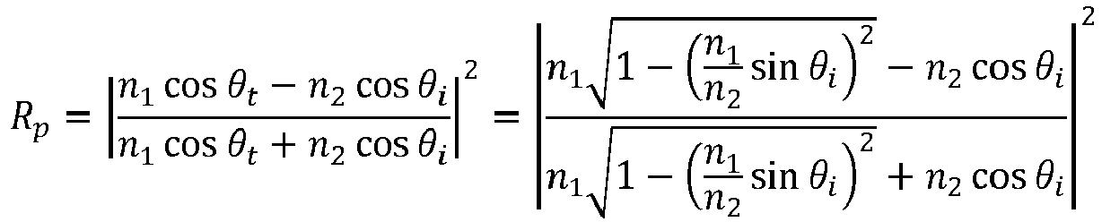
- For moderate angles of incidence, there is a considerable difference in reflection coefficient between the s-polarised and p-polarised directions. Thus, polarised light can be used to provide greater selectivity as a function of collected coolant level.
- As an alternative to an LED, the
optical transmitter 62 may include a semiconductor laser which would result in a tightly collimated optical beam permitting a more precise predefined level of the collectedcoolant 58. - The mechanism, for detecting the leakage of coolant from the
coolant circuits discharge 76 of the collectedcoolant 58 from thecollector 60. The outlet is configured to have predetermined dimensions. Since the dimensions of the outlet are known, it becomes possible to correlate the coolant leakage flow rate with the collected coolant level in thecollector 60. As shown inFigure 8 , the outlet may be in the form of aweir 78 with a V-shaped groove on a side wall of thecollector 60. The flow rate of coolant through the V-shaped groove is proportional to the height of the collectedcoolant 58 above it. Alternatively, the outlet may be in the form of a hole in the bottom of the collector. - It will be appreciated that each numerical value given for the embodiment shown is merely chosen to help illustrate the working of the invention, and may be replaced by another numerical value.
Claims (15)
- An electrical apparatus comprising a coolant carrier (38,40) for carrying coolant, the coolant carrier (38,40) arranged to interconnect a plurality of positions in the electrical apparatus, the electrical apparatus operable so as to configure the plurality of positions to be at different electrical potentials, wherein the electrical apparatus further includes a power supply circuit (56) configured to, in use, draw a leakage current from the coolant carrier (38,40) so as to provide a power supply source for powering one or more electrical devices (100).
- An electrical apparatus according to Claim 1 including a plurality of electrical components, wherein each of the plurality of positions in the electrical apparatus corresponds to a respective one of the plurality of electrical components.
- An electrical apparatus according to Claim 2 wherein the electrical apparatus includes a plurality of additional electrical components, and the coolant carrier (38,40) is disconnected from the plurality of additional electrical components.
- An electrical apparatus according to any one of the preceding claims wherein the electrical apparatus includes a switching valve.
- An electrical apparatus according to Claim 4 wherein the switching valve includes a plurality of switching modules (32), each of the plurality of positions corresponding to a respective one of the plurality of switching modules (32) such that the coolant carrier (38,40) is arranged to interconnect the plurality of switching modules (32).
- An electrical apparatus according to any one of the preceding claims wherein the coolant carrier (38,40) is arranged to interconnect the plurality of positions such that, in use of the electrical apparatus, the coolant carrier (38,40) forms an electrically balanced circuit.
- An electrical apparatus according to Claim 6 further including an electrically conductive member, wherein the coolant carrier (38,40) is arranged to interconnect the plurality of positions and the electrically conductive member such that, in use of the electrical apparatus, the coolant carrier (38,40) forms an electrically balanced circuit.
- An electrical apparatus according to any one of the preceding claims further including an electric field shielding member (36), wherein the coolant carrier (38,40) is configured to be connected to the electric field shielding member (36).
- An electrical apparatus according to Claim 8 when dependent from Claim 7 wherein the electrically conductive member is or includes the electric field shielding member (36).
- An electrical apparatus according to Claim 8 or Claim 9 wherein the electric field shielding member (36) is arranged at one end of the electrical apparatus.
- An electrical apparatus according to Claim 10 in combination with Claim 5, wherein the electric field shielding member (36) is arranged at one end of the plurality of switching modules (32).
- An electrical apparatus according to any one of the preceding claims wherein the coolant carrier (38,40) includes first and second coolant carrier portions, each of the first and second coolant carrier portions arranged to interconnect the plurality of positions, the first and second coolant carrier portions being in fluid communication with each other.
- An electrical apparatus according to any one of the preceding claims further including a collector (60) arranged to collect leaked or spilt coolant from the coolant carrier (38,40), and the electrical apparatus further includes a monitoring device configured to monitor a level of collected coolant (58) in the collector (60), wherein the collector (60) includes an outlet for permitting discharge (76) of the collected coolant (58) from the collector (60).
- An electrical apparatus according to Claim 13 wherein the monitoring device includes an optical source (62) configured to direct light (68) towards a surface of the collected coolant (58) in the collector (60), and the monitoring device further includes an optical sensor (64) configured to detect light (70) reflected off the surface of the collected coolant (58) in the collector (60).
- An electrical apparatus according to Claim 14 or Claim 15 wherein the outlet is in the form of a weir (78), or the outlet is in the form of a hole in a base of the collector.
Priority Applications (3)
| Application Number | Priority Date | Filing Date | Title |
|---|---|---|---|
| EP18161349.8A EP3540928B1 (en) | 2018-03-13 | 2018-03-13 | Electrical apparatus |
| PCT/EP2019/055779 WO2019175030A1 (en) | 2018-03-13 | 2019-03-07 | Electrical apparatus |
| CN201980018791.1A CN111819780A (en) | 2018-03-13 | 2019-03-07 | Electrical Equipment |
Applications Claiming Priority (1)
| Application Number | Priority Date | Filing Date | Title |
|---|---|---|---|
| EP18161349.8A EP3540928B1 (en) | 2018-03-13 | 2018-03-13 | Electrical apparatus |
Publications (2)
| Publication Number | Publication Date |
|---|---|
| EP3540928A1 true EP3540928A1 (en) | 2019-09-18 |
| EP3540928B1 EP3540928B1 (en) | 2022-02-09 |
Family
ID=61691650
Family Applications (1)
| Application Number | Title | Priority Date | Filing Date |
|---|---|---|---|
| EP18161349.8A Not-in-force EP3540928B1 (en) | 2018-03-13 | 2018-03-13 | Electrical apparatus |
Country Status (3)
| Country | Link |
|---|---|
| EP (1) | EP3540928B1 (en) |
| CN (1) | CN111819780A (en) |
| WO (1) | WO2019175030A1 (en) |
Citations (5)
| Publication number | Priority date | Publication date | Assignee | Title |
|---|---|---|---|---|
| JPS5788751A (en) * | 1980-11-21 | 1982-06-02 | Toshiba Corp | Leakage current monitor |
| US20100020452A1 (en) * | 2008-07-24 | 2010-01-28 | Technology Research Corporation | Leakage current detection and interruption circuit powered by leakage current |
| WO2017007229A1 (en) * | 2015-07-06 | 2017-01-12 | 엘지이노텍(주) | Automatic water supply device |
| GB2544820A (en) * | 2015-11-30 | 2017-05-31 | Tridonic Gmbh & Co Kg | A low voltage power supply using an earth connection on a terminal block |
| US20180010833A1 (en) * | 2016-07-07 | 2018-01-11 | Trane International Inc. | Accumulator for charge management |
Family Cites Families (1)
| Publication number | Priority date | Publication date | Assignee | Title |
|---|---|---|---|---|
| JP2006100005A (en) * | 2004-09-28 | 2006-04-13 | Toyota Motor Corp | Fuel cell leakage detection device |
-
2018
- 2018-03-13 EP EP18161349.8A patent/EP3540928B1/en not_active Not-in-force
-
2019
- 2019-03-07 WO PCT/EP2019/055779 patent/WO2019175030A1/en not_active Ceased
- 2019-03-07 CN CN201980018791.1A patent/CN111819780A/en active Pending
Patent Citations (5)
| Publication number | Priority date | Publication date | Assignee | Title |
|---|---|---|---|---|
| JPS5788751A (en) * | 1980-11-21 | 1982-06-02 | Toshiba Corp | Leakage current monitor |
| US20100020452A1 (en) * | 2008-07-24 | 2010-01-28 | Technology Research Corporation | Leakage current detection and interruption circuit powered by leakage current |
| WO2017007229A1 (en) * | 2015-07-06 | 2017-01-12 | 엘지이노텍(주) | Automatic water supply device |
| GB2544820A (en) * | 2015-11-30 | 2017-05-31 | Tridonic Gmbh & Co Kg | A low voltage power supply using an earth connection on a terminal block |
| US20180010833A1 (en) * | 2016-07-07 | 2018-01-11 | Trane International Inc. | Accumulator for charge management |
Also Published As
| Publication number | Publication date |
|---|---|
| WO2019175030A1 (en) | 2019-09-19 |
| CN111819780A (en) | 2020-10-23 |
| EP3540928B1 (en) | 2022-02-09 |
Similar Documents
| Publication | Publication Date | Title |
|---|---|---|
| CN107037302B (en) | Fault Detection Systems and Circuits | |
| CN104578429B (en) | Online operation monitoring system for cable branch box | |
| CN104702208B (en) | Photovoltaic array ground insulation resistance online detecting system for high-power photovoltaic inverter | |
| WO2012026449A1 (en) | Earth-fault detection device, collector box using earth-fault detection device, and photovoltaic power generation device using collector box | |
| KR101245827B1 (en) | Diagnostic apparatus for shadow and defect of pv module using mic | |
| DK2904676T3 (en) | Method for monitoring multiple electrical power lines of a wire string | |
| EP3058636A1 (en) | Converters for wind turbine generators | |
| CN102742022A (en) | Photovoltaic power generation system | |
| US12003095B2 (en) | Abnormality detecting system for a solar power grid | |
| EP3540928B1 (en) | Electrical apparatus | |
| US20120256754A1 (en) | Monitoring device for an ungrounded power network of a photovoltaic system | |
| KR101899080B1 (en) | A module for photovoltaic connection board | |
| EP2837076B1 (en) | Neutral grounding resistor monitor | |
| US10408865B2 (en) | Power monitor protective shroud | |
| KR102646351B1 (en) | Solar power generation system and method capable of detecting leakage section through leakage monitoring for each solar cell module | |
| CN206727443U (en) | A kind of device of inside switch cabinet temperature rise monitoring | |
| KR101582825B1 (en) | Monitoring apparatus for solar cell | |
| CN215526041U (en) | Detection device for primary and secondary fusion switch and primary and secondary electrical cabinet | |
| CN210894485U (en) | Rectifier cabinet current temperature detection management system | |
| EP4182643B1 (en) | Fault gas detection system for a liquid filled high voltage transformer | |
| KR101307939B1 (en) | Incoming panel for protecting current transformer | |
| CN210689867U (en) | Temperature sensing cable detection device | |
| CN205282264U (en) | Outdoor current transformer of open -type | |
| JPH06165371A (en) | Water cooled thyristor valve | |
| CN118282045A (en) | Voltage parallel cabinet for switch station of pumped storage power station |
Legal Events
| Date | Code | Title | Description |
|---|---|---|---|
| PUAI | Public reference made under article 153(3) epc to a published international application that has entered the european phase |
Free format text: ORIGINAL CODE: 0009012 |
|
| STAA | Information on the status of an ep patent application or granted ep patent |
Free format text: STATUS: THE APPLICATION HAS BEEN PUBLISHED |
|
| AK | Designated contracting states |
Kind code of ref document: A1 Designated state(s): AL AT BE BG CH CY CZ DE DK EE ES FI FR GB GR HR HU IE IS IT LI LT LU LV MC MK MT NL NO PL PT RO RS SE SI SK SM TR |
|
| AX | Request for extension of the european patent |
Extension state: BA ME |
|
| STAA | Information on the status of an ep patent application or granted ep patent |
Free format text: STATUS: REQUEST FOR EXAMINATION WAS MADE |
|
| 17P | Request for examination filed |
Effective date: 20200310 |
|
| RBV | Designated contracting states (corrected) |
Designated state(s): AL AT BE BG CH CY CZ DE DK EE ES FI FR GB GR HR HU IE IS IT LI LT LU LV MC MK MT NL NO PL PT RO RS SE SI SK SM TR |
|
| STAA | Information on the status of an ep patent application or granted ep patent |
Free format text: STATUS: EXAMINATION IS IN PROGRESS |
|
| 17Q | First examination report despatched |
Effective date: 20201028 |
|
| GRAP | Despatch of communication of intention to grant a patent |
Free format text: ORIGINAL CODE: EPIDOSNIGR1 |
|
| STAA | Information on the status of an ep patent application or granted ep patent |
Free format text: STATUS: GRANT OF PATENT IS INTENDED |
|
| INTG | Intention to grant announced |
Effective date: 20210611 |
|
| GRAJ | Information related to disapproval of communication of intention to grant by the applicant or resumption of examination proceedings by the epo deleted |
Free format text: ORIGINAL CODE: EPIDOSDIGR1 |
|
| STAA | Information on the status of an ep patent application or granted ep patent |
Free format text: STATUS: EXAMINATION IS IN PROGRESS |
|
| INTC | Intention to grant announced (deleted) | ||
| GRAP | Despatch of communication of intention to grant a patent |
Free format text: ORIGINAL CODE: EPIDOSNIGR1 |
|
| STAA | Information on the status of an ep patent application or granted ep patent |
Free format text: STATUS: GRANT OF PATENT IS INTENDED |
|
| INTG | Intention to grant announced |
Effective date: 20210910 |
|
| GRAS | Grant fee paid |
Free format text: ORIGINAL CODE: EPIDOSNIGR3 |
|
| GRAA | (expected) grant |
Free format text: ORIGINAL CODE: 0009210 |
|
| STAA | Information on the status of an ep patent application or granted ep patent |
Free format text: STATUS: THE PATENT HAS BEEN GRANTED |
|
| AK | Designated contracting states |
Kind code of ref document: B1 Designated state(s): AL AT BE BG CH CY CZ DE DK EE ES FI FR GB GR HR HU IE IS IT LI LT LU LV MC MK MT NL NO PL PT RO RS SE SI SK SM TR |
|
| REG | Reference to a national code |
Ref country code: GB Ref legal event code: FG4D |
|
| REG | Reference to a national code |
Ref country code: CH Ref legal event code: EP Ref country code: AT Ref legal event code: REF Ref document number: 1468123 Country of ref document: AT Kind code of ref document: T Effective date: 20220215 |
|
| REG | Reference to a national code |
Ref country code: DE Ref legal event code: R096 Ref document number: 602018030492 Country of ref document: DE |
|
| REG | Reference to a national code |
Ref country code: IE Ref legal event code: FG4D |
|
| PGFP | Annual fee paid to national office [announced via postgrant information from national office to epo] |
Ref country code: GB Payment date: 20220323 Year of fee payment: 5 Ref country code: DE Payment date: 20220217 Year of fee payment: 5 |
|
| REG | Reference to a national code |
Ref country code: SE Ref legal event code: TRGR |
|
| REG | Reference to a national code |
Ref country code: LT Ref legal event code: MG9D |
|
| REG | Reference to a national code |
Ref country code: NL Ref legal event code: MP Effective date: 20220209 |
|
| REG | Reference to a national code |
Ref country code: AT Ref legal event code: MK05 Ref document number: 1468123 Country of ref document: AT Kind code of ref document: T Effective date: 20220209 |
|
| PG25 | Lapsed in a contracting state [announced via postgrant information from national office to epo] |
Ref country code: RS Free format text: LAPSE BECAUSE OF FAILURE TO SUBMIT A TRANSLATION OF THE DESCRIPTION OR TO PAY THE FEE WITHIN THE PRESCRIBED TIME-LIMIT Effective date: 20220209 Ref country code: PT Free format text: LAPSE BECAUSE OF FAILURE TO SUBMIT A TRANSLATION OF THE DESCRIPTION OR TO PAY THE FEE WITHIN THE PRESCRIBED TIME-LIMIT Effective date: 20220609 Ref country code: NO Free format text: LAPSE BECAUSE OF FAILURE TO SUBMIT A TRANSLATION OF THE DESCRIPTION OR TO PAY THE FEE WITHIN THE PRESCRIBED TIME-LIMIT Effective date: 20220509 Ref country code: NL Free format text: LAPSE BECAUSE OF FAILURE TO SUBMIT A TRANSLATION OF THE DESCRIPTION OR TO PAY THE FEE WITHIN THE PRESCRIBED TIME-LIMIT Effective date: 20220209 Ref country code: LT Free format text: LAPSE BECAUSE OF FAILURE TO SUBMIT A TRANSLATION OF THE DESCRIPTION OR TO PAY THE FEE WITHIN THE PRESCRIBED TIME-LIMIT Effective date: 20220209 Ref country code: HR Free format text: LAPSE BECAUSE OF FAILURE TO SUBMIT A TRANSLATION OF THE DESCRIPTION OR TO PAY THE FEE WITHIN THE PRESCRIBED TIME-LIMIT Effective date: 20220209 Ref country code: ES Free format text: LAPSE BECAUSE OF FAILURE TO SUBMIT A TRANSLATION OF THE DESCRIPTION OR TO PAY THE FEE WITHIN THE PRESCRIBED TIME-LIMIT Effective date: 20220209 Ref country code: BG Free format text: LAPSE BECAUSE OF FAILURE TO SUBMIT A TRANSLATION OF THE DESCRIPTION OR TO PAY THE FEE WITHIN THE PRESCRIBED TIME-LIMIT Effective date: 20220509 |
|
| PG25 | Lapsed in a contracting state [announced via postgrant information from national office to epo] |
Ref country code: PL Free format text: LAPSE BECAUSE OF FAILURE TO SUBMIT A TRANSLATION OF THE DESCRIPTION OR TO PAY THE FEE WITHIN THE PRESCRIBED TIME-LIMIT Effective date: 20220209 Ref country code: LV Free format text: LAPSE BECAUSE OF FAILURE TO SUBMIT A TRANSLATION OF THE DESCRIPTION OR TO PAY THE FEE WITHIN THE PRESCRIBED TIME-LIMIT Effective date: 20220209 Ref country code: GR Free format text: LAPSE BECAUSE OF FAILURE TO SUBMIT A TRANSLATION OF THE DESCRIPTION OR TO PAY THE FEE WITHIN THE PRESCRIBED TIME-LIMIT Effective date: 20220510 Ref country code: FI Free format text: LAPSE BECAUSE OF FAILURE TO SUBMIT A TRANSLATION OF THE DESCRIPTION OR TO PAY THE FEE WITHIN THE PRESCRIBED TIME-LIMIT Effective date: 20220209 Ref country code: AT Free format text: LAPSE BECAUSE OF FAILURE TO SUBMIT A TRANSLATION OF THE DESCRIPTION OR TO PAY THE FEE WITHIN THE PRESCRIBED TIME-LIMIT Effective date: 20220209 |
|
| PG25 | Lapsed in a contracting state [announced via postgrant information from national office to epo] |
Ref country code: IS Free format text: LAPSE BECAUSE OF FAILURE TO SUBMIT A TRANSLATION OF THE DESCRIPTION OR TO PAY THE FEE WITHIN THE PRESCRIBED TIME-LIMIT Effective date: 20220609 |
|
| PG25 | Lapsed in a contracting state [announced via postgrant information from national office to epo] |
Ref country code: SM Free format text: LAPSE BECAUSE OF FAILURE TO SUBMIT A TRANSLATION OF THE DESCRIPTION OR TO PAY THE FEE WITHIN THE PRESCRIBED TIME-LIMIT Effective date: 20220209 Ref country code: SK Free format text: LAPSE BECAUSE OF FAILURE TO SUBMIT A TRANSLATION OF THE DESCRIPTION OR TO PAY THE FEE WITHIN THE PRESCRIBED TIME-LIMIT Effective date: 20220209 Ref country code: RO Free format text: LAPSE BECAUSE OF FAILURE TO SUBMIT A TRANSLATION OF THE DESCRIPTION OR TO PAY THE FEE WITHIN THE PRESCRIBED TIME-LIMIT Effective date: 20220209 Ref country code: EE Free format text: LAPSE BECAUSE OF FAILURE TO SUBMIT A TRANSLATION OF THE DESCRIPTION OR TO PAY THE FEE WITHIN THE PRESCRIBED TIME-LIMIT Effective date: 20220209 Ref country code: DK Free format text: LAPSE BECAUSE OF FAILURE TO SUBMIT A TRANSLATION OF THE DESCRIPTION OR TO PAY THE FEE WITHIN THE PRESCRIBED TIME-LIMIT Effective date: 20220209 Ref country code: CZ Free format text: LAPSE BECAUSE OF FAILURE TO SUBMIT A TRANSLATION OF THE DESCRIPTION OR TO PAY THE FEE WITHIN THE PRESCRIBED TIME-LIMIT Effective date: 20220209 |
|
| REG | Reference to a national code |
Ref country code: CH Ref legal event code: PL |
|
| REG | Reference to a national code |
Ref country code: DE Ref legal event code: R097 Ref document number: 602018030492 Country of ref document: DE |
|
| PG25 | Lapsed in a contracting state [announced via postgrant information from national office to epo] |
Ref country code: MC Free format text: LAPSE BECAUSE OF FAILURE TO SUBMIT A TRANSLATION OF THE DESCRIPTION OR TO PAY THE FEE WITHIN THE PRESCRIBED TIME-LIMIT Effective date: 20220209 Ref country code: AL Free format text: LAPSE BECAUSE OF FAILURE TO SUBMIT A TRANSLATION OF THE DESCRIPTION OR TO PAY THE FEE WITHIN THE PRESCRIBED TIME-LIMIT Effective date: 20220209 |
|
| REG | Reference to a national code |
Ref country code: BE Ref legal event code: MM Effective date: 20220331 |
|
| PLBE | No opposition filed within time limit |
Free format text: ORIGINAL CODE: 0009261 |
|
| STAA | Information on the status of an ep patent application or granted ep patent |
Free format text: STATUS: NO OPPOSITION FILED WITHIN TIME LIMIT |
|
| 26N | No opposition filed |
Effective date: 20221110 |
|
| PG25 | Lapsed in a contracting state [announced via postgrant information from national office to epo] |
Ref country code: LU Free format text: LAPSE BECAUSE OF NON-PAYMENT OF DUE FEES Effective date: 20220313 Ref country code: LI Free format text: LAPSE BECAUSE OF NON-PAYMENT OF DUE FEES Effective date: 20220331 Ref country code: IE Free format text: LAPSE BECAUSE OF NON-PAYMENT OF DUE FEES Effective date: 20220313 Ref country code: FR Free format text: LAPSE BECAUSE OF NON-PAYMENT OF DUE FEES Effective date: 20220409 Ref country code: CH Free format text: LAPSE BECAUSE OF NON-PAYMENT OF DUE FEES Effective date: 20220331 |
|
| PG25 | Lapsed in a contracting state [announced via postgrant information from national office to epo] |
Ref country code: SI Free format text: LAPSE BECAUSE OF FAILURE TO SUBMIT A TRANSLATION OF THE DESCRIPTION OR TO PAY THE FEE WITHIN THE PRESCRIBED TIME-LIMIT Effective date: 20220209 Ref country code: BE Free format text: LAPSE BECAUSE OF NON-PAYMENT OF DUE FEES Effective date: 20220331 |
|
| PG25 | Lapsed in a contracting state [announced via postgrant information from national office to epo] |
Ref country code: IT Free format text: LAPSE BECAUSE OF FAILURE TO SUBMIT A TRANSLATION OF THE DESCRIPTION OR TO PAY THE FEE WITHIN THE PRESCRIBED TIME-LIMIT Effective date: 20220209 |
|
| PGFP | Annual fee paid to national office [announced via postgrant information from national office to epo] |
Ref country code: SE Payment date: 20220217 Year of fee payment: 5 |
|
| REG | Reference to a national code |
Ref country code: DE Ref legal event code: R119 Ref document number: 602018030492 Country of ref document: DE |
|
| REG | Reference to a national code |
Ref country code: SE Ref legal event code: EUG |
|
| GBPC | Gb: european patent ceased through non-payment of renewal fee |
Effective date: 20230313 |
|
| PG25 | Lapsed in a contracting state [announced via postgrant information from national office to epo] |
Ref country code: GB Free format text: LAPSE BECAUSE OF NON-PAYMENT OF DUE FEES Effective date: 20230313 |
|
| PG25 | Lapsed in a contracting state [announced via postgrant information from national office to epo] |
Ref country code: SE Free format text: LAPSE BECAUSE OF NON-PAYMENT OF DUE FEES Effective date: 20230314 Ref country code: GB Free format text: LAPSE BECAUSE OF NON-PAYMENT OF DUE FEES Effective date: 20230313 Ref country code: DE Free format text: LAPSE BECAUSE OF NON-PAYMENT OF DUE FEES Effective date: 20231003 |
|
| PG25 | Lapsed in a contracting state [announced via postgrant information from national office to epo] |
Ref country code: MK Free format text: LAPSE BECAUSE OF FAILURE TO SUBMIT A TRANSLATION OF THE DESCRIPTION OR TO PAY THE FEE WITHIN THE PRESCRIBED TIME-LIMIT Effective date: 20220209 Ref country code: CY Free format text: LAPSE BECAUSE OF FAILURE TO SUBMIT A TRANSLATION OF THE DESCRIPTION OR TO PAY THE FEE WITHIN THE PRESCRIBED TIME-LIMIT Effective date: 20220209 |
|
| PG25 | Lapsed in a contracting state [announced via postgrant information from national office to epo] |
Ref country code: HU Free format text: LAPSE BECAUSE OF FAILURE TO SUBMIT A TRANSLATION OF THE DESCRIPTION OR TO PAY THE FEE WITHIN THE PRESCRIBED TIME-LIMIT; INVALID AB INITIO Effective date: 20180313 |
|
| PG25 | Lapsed in a contracting state [announced via postgrant information from national office to epo] |
Ref country code: MT Free format text: LAPSE BECAUSE OF FAILURE TO SUBMIT A TRANSLATION OF THE DESCRIPTION OR TO PAY THE FEE WITHIN THE PRESCRIBED TIME-LIMIT Effective date: 20220209 |
|
| PG25 | Lapsed in a contracting state [announced via postgrant information from national office to epo] |
Ref country code: TR Free format text: LAPSE BECAUSE OF FAILURE TO SUBMIT A TRANSLATION OF THE DESCRIPTION OR TO PAY THE FEE WITHIN THE PRESCRIBED TIME-LIMIT Effective date: 20220209 |