EP3540798A1 - Piezoelectric element and liquid ejection head - Google Patents
Piezoelectric element and liquid ejection head Download PDFInfo
- Publication number
- EP3540798A1 EP3540798A1 EP19162930.2A EP19162930A EP3540798A1 EP 3540798 A1 EP3540798 A1 EP 3540798A1 EP 19162930 A EP19162930 A EP 19162930A EP 3540798 A1 EP3540798 A1 EP 3540798A1
- Authority
- EP
- European Patent Office
- Prior art keywords
- layer
- piezoelectric
- orientation control
- electrode
- control layer
- Prior art date
- Legal status (The legal status is an assumption and is not a legal conclusion. Google has not performed a legal analysis and makes no representation as to the accuracy of the status listed.)
- Granted
Links
Images





Classifications
-
- H—ELECTRICITY
- H10—SEMICONDUCTOR DEVICES; ELECTRIC SOLID-STATE DEVICES NOT OTHERWISE PROVIDED FOR
- H10N—ELECTRIC SOLID-STATE DEVICES NOT OTHERWISE PROVIDED FOR
- H10N30/00—Piezoelectric or electrostrictive devices
- H10N30/704—Piezoelectric or electrostrictive devices based on piezoelectric or electrostrictive films or coatings
- H10N30/706—Piezoelectric or electrostrictive devices based on piezoelectric or electrostrictive films or coatings characterised by the underlying bases, e.g. substrates
- H10N30/708—Intermediate layers, e.g. barrier, adhesion or growth control buffer layers
-
- H—ELECTRICITY
- H10—SEMICONDUCTOR DEVICES; ELECTRIC SOLID-STATE DEVICES NOT OTHERWISE PROVIDED FOR
- H10N—ELECTRIC SOLID-STATE DEVICES NOT OTHERWISE PROVIDED FOR
- H10N30/00—Piezoelectric or electrostrictive devices
- H10N30/80—Constructional details
- H10N30/85—Piezoelectric or electrostrictive active materials
- H10N30/853—Ceramic compositions
- H10N30/8548—Lead-based oxides
- H10N30/8554—Lead-zirconium titanate [PZT] based
-
- B—PERFORMING OPERATIONS; TRANSPORTING
- B41—PRINTING; LINING MACHINES; TYPEWRITERS; STAMPS
- B41J—TYPEWRITERS; SELECTIVE PRINTING MECHANISMS, i.e. MECHANISMS PRINTING OTHERWISE THAN FROM A FORME; CORRECTION OF TYPOGRAPHICAL ERRORS
- B41J2/00—Typewriters or selective printing mechanisms characterised by the printing or marking process for which they are designed
- B41J2/005—Typewriters or selective printing mechanisms characterised by the printing or marking process for which they are designed characterised by bringing liquid or particles selectively into contact with a printing material
- B41J2/01—Ink jet
- B41J2/135—Nozzles
- B41J2/14—Structure thereof only for on-demand ink jet heads
- B41J2/14201—Structure of print heads with piezoelectric elements
-
- B—PERFORMING OPERATIONS; TRANSPORTING
- B41—PRINTING; LINING MACHINES; TYPEWRITERS; STAMPS
- B41J—TYPEWRITERS; SELECTIVE PRINTING MECHANISMS, i.e. MECHANISMS PRINTING OTHERWISE THAN FROM A FORME; CORRECTION OF TYPOGRAPHICAL ERRORS
- B41J2/00—Typewriters or selective printing mechanisms characterised by the printing or marking process for which they are designed
- B41J2/005—Typewriters or selective printing mechanisms characterised by the printing or marking process for which they are designed characterised by bringing liquid or particles selectively into contact with a printing material
- B41J2/01—Ink jet
- B41J2/135—Nozzles
- B41J2/14—Structure thereof only for on-demand ink jet heads
- B41J2/14201—Structure of print heads with piezoelectric elements
- B41J2/14233—Structure of print heads with piezoelectric elements of film type, deformed by bending and disposed on a diaphragm
-
- H—ELECTRICITY
- H10—SEMICONDUCTOR DEVICES; ELECTRIC SOLID-STATE DEVICES NOT OTHERWISE PROVIDED FOR
- H10N—ELECTRIC SOLID-STATE DEVICES NOT OTHERWISE PROVIDED FOR
- H10N30/00—Piezoelectric or electrostrictive devices
- H10N30/50—Piezoelectric or electrostrictive devices having a stacked or multilayer structure
-
- H—ELECTRICITY
- H10—SEMICONDUCTOR DEVICES; ELECTRIC SOLID-STATE DEVICES NOT OTHERWISE PROVIDED FOR
- H10N—ELECTRIC SOLID-STATE DEVICES NOT OTHERWISE PROVIDED FOR
- H10N30/00—Piezoelectric or electrostrictive devices
- H10N30/50—Piezoelectric or electrostrictive devices having a stacked or multilayer structure
- H10N30/508—Piezoelectric or electrostrictive devices having a stacked or multilayer structure adapted for alleviating internal stress, e.g. cracking control layers
-
- H—ELECTRICITY
- H10—SEMICONDUCTOR DEVICES; ELECTRIC SOLID-STATE DEVICES NOT OTHERWISE PROVIDED FOR
- H10N—ELECTRIC SOLID-STATE DEVICES NOT OTHERWISE PROVIDED FOR
- H10N30/00—Piezoelectric or electrostrictive devices
- H10N30/80—Constructional details
- H10N30/87—Electrodes or interconnections, e.g. leads or terminals
- H10N30/872—Interconnections, e.g. connection electrodes of multilayer piezoelectric or electrostrictive devices
-
- B—PERFORMING OPERATIONS; TRANSPORTING
- B41—PRINTING; LINING MACHINES; TYPEWRITERS; STAMPS
- B41J—TYPEWRITERS; SELECTIVE PRINTING MECHANISMS, i.e. MECHANISMS PRINTING OTHERWISE THAN FROM A FORME; CORRECTION OF TYPOGRAPHICAL ERRORS
- B41J2/00—Typewriters or selective printing mechanisms characterised by the printing or marking process for which they are designed
- B41J2/005—Typewriters or selective printing mechanisms characterised by the printing or marking process for which they are designed characterised by bringing liquid or particles selectively into contact with a printing material
- B41J2/01—Ink jet
- B41J2/135—Nozzles
- B41J2/14—Structure thereof only for on-demand ink jet heads
- B41J2/14201—Structure of print heads with piezoelectric elements
- B41J2/14233—Structure of print heads with piezoelectric elements of film type, deformed by bending and disposed on a diaphragm
- B41J2002/14241—Structure of print heads with piezoelectric elements of film type, deformed by bending and disposed on a diaphragm having a cover around the piezoelectric thin film element
-
- B—PERFORMING OPERATIONS; TRANSPORTING
- B41—PRINTING; LINING MACHINES; TYPEWRITERS; STAMPS
- B41J—TYPEWRITERS; SELECTIVE PRINTING MECHANISMS, i.e. MECHANISMS PRINTING OTHERWISE THAN FROM A FORME; CORRECTION OF TYPOGRAPHICAL ERRORS
- B41J2/00—Typewriters or selective printing mechanisms characterised by the printing or marking process for which they are designed
- B41J2/005—Typewriters or selective printing mechanisms characterised by the printing or marking process for which they are designed characterised by bringing liquid or particles selectively into contact with a printing material
- B41J2/01—Ink jet
- B41J2/135—Nozzles
- B41J2/14—Structure thereof only for on-demand ink jet heads
- B41J2/14201—Structure of print heads with piezoelectric elements
- B41J2/14233—Structure of print heads with piezoelectric elements of film type, deformed by bending and disposed on a diaphragm
- B41J2002/14258—Multi layer thin film type piezoelectric element
-
- H—ELECTRICITY
- H10—SEMICONDUCTOR DEVICES; ELECTRIC SOLID-STATE DEVICES NOT OTHERWISE PROVIDED FOR
- H10N—ELECTRIC SOLID-STATE DEVICES NOT OTHERWISE PROVIDED FOR
- H10N30/00—Piezoelectric or electrostrictive devices
- H10N30/01—Manufacture or treatment
- H10N30/07—Forming of piezoelectric or electrostrictive parts or bodies on an electrical element or another base
- H10N30/074—Forming of piezoelectric or electrostrictive parts or bodies on an electrical element or another base by depositing piezoelectric or electrostrictive layers, e.g. aerosol or screen printing
- H10N30/077—Forming of piezoelectric or electrostrictive parts or bodies on an electrical element or another base by depositing piezoelectric or electrostrictive layers, e.g. aerosol or screen printing by liquid phase deposition
- H10N30/078—Forming of piezoelectric or electrostrictive parts or bodies on an electrical element or another base by depositing piezoelectric or electrostrictive layers, e.g. aerosol or screen printing by liquid phase deposition by sol-gel deposition
-
- H—ELECTRICITY
- H10—SEMICONDUCTOR DEVICES; ELECTRIC SOLID-STATE DEVICES NOT OTHERWISE PROVIDED FOR
- H10N—ELECTRIC SOLID-STATE DEVICES NOT OTHERWISE PROVIDED FOR
- H10N30/00—Piezoelectric or electrostrictive devices
- H10N30/01—Manufacture or treatment
- H10N30/07—Forming of piezoelectric or electrostrictive parts or bodies on an electrical element or another base
- H10N30/074—Forming of piezoelectric or electrostrictive parts or bodies on an electrical element or another base by depositing piezoelectric or electrostrictive layers, e.g. aerosol or screen printing
- H10N30/079—Forming of piezoelectric or electrostrictive parts or bodies on an electrical element or another base by depositing piezoelectric or electrostrictive layers, e.g. aerosol or screen printing using intermediate layers, e.g. for growth control
Definitions
- the present invention relates to a piezoelectric element and a liquid ejection head.
- a piezoelectric element typically includes a piezoelectric layer capable of electromechanical conversion, and two electrodes between which the piezoelectric element is disposed.
- the piezoelectric element may be used, for example, in a liquid ejection head mounted in an ink jet recording apparatus.
- the piezoelectric layer contains lead zirconate titanate (PZT) or any other compound, and many of the possible materials of the piezoelectric layer have a perovskite crystal structure.
- a thin piezoelectric layer has a structure in which many crystals (crystal grains) are arranged. It has been studied to increase the piezoelectric constant of individual crystals in the thin layer from the viewpoint of increasing the displacement of the piezoelectric layer. For example, in JP-A-2011-233817 , lattice distortion (c/a) of the crystals in a piezoelectric body is controlled from the viewpoint of improving the piezoelectric properties and dielectric properties of the piezoelectric body.
- the piezoelectric properties of a piezoelectric element vary depending on many factors, such as composition, crystal structure, crystal orientation, lattice distortion, domain structure, thickness, and structure at the interface with the electrode. Therefore, merely controlling c/a while focusing on the crystals of the piezoelectric material, as disclosed in the foregoing JP-A-2011-233817 , does not sufficiently allow the piezoelectric element to exhibit a large displacement.
- a piezoelectric element including a first electrode disposed over a substrate, an orientation control layer disposed over the first electrode and containing titanium, a piezoelectric layer disposed over the orientation control layer and having a perovskite crystal structure, and a second electrode disposed over the piezoelectric layer.
- the orientation control layer has a thickness in the range of 5.0 nm to 22.0 nm.
- the orientation control layer may have a thickness in the range of 6.85 nm to 21.5 nm.
- the piezoelectric element may further include an additional piezoelectric layer having a perovskite crystal structure between the first electrode and the orientation control layer.
- the total thickness of the piezoelectric layer, the orientation control layer, and the additional piezoelectric layer may be 1.0 ⁇ m or less.
- the first electrode may have a thickness in the range of 50 nm to 140 nm.
- the orientation control layer may contain lead and titanium.
- the second electrode may be a common electrode shared with another piezoelectric element.
- a liquid ejection head including the piezoelectric element described above is provided.
- Fig. 1 is a schematic sectional view of a piezoelectric element 100 according to an embodiment of the invention.
- the piezoelectric element 100 includes a first electrode 10, a first orientation control layer 15, a first piezoelectric layer 20, a second orientation control layer 30, a second piezoelectric layer 40, and a second electrode 50.
- the first electrode 10 is one of the electrodes operable to apply voltage to the first orientation control layer 15, the first piezoelectric layer 20, the second orientation control layer 30, and the second piezoelectric layer 40.
- the first electrode 10 may be referred to as the lower electrode.
- the first electrode 10 is disposed on a substrate 2 (vibration plate 230).
- the first electrode 10 may be in the form of a layer.
- the thickness of the first electrode 10 depends on the size of the piezoelectric element 100 and, in an embodiment, may be in the range of 3 nm to 300 nm, preferably in the range of 50 nm to 140 nm.
- small piezoelectric elements 100 are densely arranged. In a small piezoelectric element 100, as the thickness of the piezoelectric element 100 becomes smaller, the vibration plate is more efficiently driven.
- the total thickness of the first piezoelectric layer 20, the second orientation control layer 30, and the second piezoelectric layer 40 may be 1 ⁇ m or less.
- the thickness of the first electrode 10 may also be reduced in the range of 10 nm to 200 nm, preferably 30 nm to 150 nm or 40 nm to 100 nm.
- the first electrode 10 may contain a platinum group element.
- Platinum group elements are Groups 8, 9 and 10 elements in the fifth and sixth periods in the periodic table and include ruthenium, rhodium, palladium, osmium, iridium, and platinum.
- the first electrode 10 may have a multilayer structure including a platinum layer and an iridium layer that are formed in this order from the side opposite the first piezoelectric layer 20 (the side closer to the substrate 2).
- the iridium layer is a layer containing iridium as a major constituent
- the platinum layer is a layer containing platinum as a major constituent.
- the term "major constituent" of a member or a portion implies that the content of the element of interest accounts for 80% or more (preferably 90% or more, 95% or more, or 98% or more) of the total amount of the elements in the member or portion.
- the material of the first electrode 10 is not particularly limited provided that it is electrically conductive and may be a metal or an electrically conductive oxide.
- the first electrode 10 may be a multilayer composite defined by a plurality of layers made of such materials.
- a first electrode 10 including a platinum layer and an iridium layer in this order from the side opposite the first piezoelectric layer 20 (the side closer to the substrate 2) can act as a barrier, for example, to hinder more effectively one or more constituents of the first piezoelectric layer 20 from penetrating the first electrode 10 and diffusing.
- the first electrode 10 is a discrete electrode separating the active portion 101 of a piezoelectric element 100 from the active portions of the other piezoelectric elements.
- the active portion 101 is the overlap between the first electrode 10 and the second electrode 50 when viewed from above.
- the portion of the piezoelectric element 100 other than the active portion 101 is referred to as the inactive portion.
- the first orientation control layer 15 is disposed over the first electrode 10. In the embodiment shown in Fig. 1 , the first orientation control layer 15 is disposed on the first electrode 10. Also, the first orientation control layer 15 lies between the first electrode 10 and the first piezoelectric layer 20. The first orientation control layer 15 controls the orientation of the crystals in the first piezoelectric layer 20.
- the thickness of the first orientation control layer 15 may be in the range of 1.0 nm to 30.0 nm and is preferably 2.0 nm to 20.0 nm.
- the first orientation control layer 15 is made of a material containing titanium.
- the material of the first orientation control layer 15 may be lead titanate or a solid solution made by substituting another element (for example, zirconium) for the titanium or the lead of lead titanate.
- the first orientation control layer 15 may be formed by depositing a titanium layer by sputtering and firing the titanium layer simultaneously with a precursor of the first piezoelectric layer 20 when the first piezoelectric layer 20 is formed. This firing changes the titanium layer into a layer containing mainly lead titanate. The layer thus prepared may be used as the first orientation control layer 15.
- the first piezoelectric layer 20 is disposed over the first electrode layer 10. In the embodiment shown in Fig. 1 , the first piezoelectric layer 20 is disposed on the first orientation control layer 15. Also, the first piezoelectric layer 20 lies between the first electrode 10 and the second orientation control layer 30.
- the thickness of the first piezoelectric layer 20 may be, for example, in the range of 100 nm to 300 nm. In an embodiment of the piezoelectric element 100 that is used in a liquid ejection head in which liquid ejection nozzles are arranged with a density as high as 400 dpi or more, the first piezoelectric layer 20 may have, for example, as small a thickness as 50 nm to 200 nm.
- the first piezoelectric layer 20 may be deformed by applying a voltage (electric field) between the first electrode 10 and the second electrode 50.
- the first piezoelectric layer 20 contains crystals having a perovskite crystal structure and produces an electromechanical conversion effect when a voltage is applied thereto.
- the first piezoelectric layer 20 may contain a substance having piezoelectric properties, for example a composite oxide having a perovskite crystal structure.
- the metal elements that may be contained in the first piezoelectric layer 20 include Pb, Ba, Ca, Nb, La, Li, Sr, Bi, Na, K, Fe, Ti, Ta, Mg, Mo, Ni, Mn, Zr, Zn, W, and Yb.
- lead zirconate titanate (PZT) containing Ti, Zr, and Pb a composite oxide (KNN) containing potassium (K), sodium (Na), and niobium (Nb), bismuth ferrate (BFO) containing Bi and Fe, or lead zirconate titanate niobate (Pb(Zr,Ti,Nb)O 3 : PZTN) may be used.
- KNN potassium
- Na sodium
- BFO bismuth ferrate
- Pb(Zr,Ti,Nb)O 3 : PZTN lead zirconate titanate niobate
- the first piezoelectric layer 20 is formed into a shape corresponding to the shape of the first electrode 10 by patterning. Therefore, the portion of the first piezoelectric layer 20 lying under the second electrode 50 is located in the active portion 101.
- the first piezoelectric layer 20 is defined by a mass of a large number of crystals (crystal grains) and is composed of preferentially ⁇ 100 ⁇ -oriented crystals.
- the phrase "preferentially ⁇ 100 ⁇ -oriented" means that all the crystals or almost all (50% or more, preferably 80% or more or 90% or more) the crystals in the piezoelectric layer are oriented in the ⁇ 100 ⁇ plane.
- the ⁇ 100 ⁇ plane includes a plurality of planes equivalent to the (100) plane.
- the c-axis extends in the direction normal to the surface of the first electrode 10 and the a-axis extends in the direction parallel to the surface of the first electrode 10, as shown in Fig. 1 .
- the a-axis may extend in any direction rotated on the c-axis.
- the piezoelectric element 100 Since the crystals in the first piezoelectric layer 20 are oriented in the ⁇ 100 ⁇ plane, the piezoelectric element 100 has piezoelectric properties.
- the crystals in the first piezoelectric layer 20 are preferentially oriented in the ⁇ 100 ⁇ plane by an operation of the first orientation control layer 15.
- the crystals in the first piezoelectric layer 20 each include polarized domains.
- a monocrystalline grain has areas having different polarization directions.
- a polarized domain refers to an area of such areas where the polarization directions are aligned.
- polarized domains are formed depending on the process of crystal growth, presence of crystal defects, recovery from crystal defects (heat treatment), and combinations of chemical elements in the piezoelectric material, but it is not clear how the polarized domains are formed.
- the crystal lattice is distorted and the crystals become tetragonal, rhombohedral, or less symmetrical than rhombohedral according to the polarization direction. Accordingly, the lattice constant of a crystal varies according to the polarization direction. Therefore, while the lattice constant of one polarized domain is constant, another polarized domain polarized in a different direction has a different lattice constant according to the polarization direction.
- the first piezoelectric layer 20 disclosed herein contains densely arranged stacking defects in an area of 3 nm or less in diameter. If the domain size is reduced due to the stacking defects, domain walls become dense. Accordingly, the relative dielectric constant increases and the response to electric field is enhanced. Also, the first piezoelectric layer 20 contains a variety of ions having different charges and ionic radiuses. Different charges cause local electric fields, and different ionic radiuses produce stresses. The domains are fixed by such local electric fields or stresses. It is thought that the first piezoelectric layer thus comes into a state having no hysteresis, that is, into a state having a relative dielectric constant independent of electric field. Whether stacking defects are present in or absent from such a very small area can be checked by, for example, nano-beam electron diffraction using a transmission electron microscope, which will be described later herein.
- subdivided nano-domains are present which contain stacking defects in an area of less than 3 nm in diameter to relieve structural distortion in the crystal grain. This causes a new dielectric polarization, enhancing response to electric field and facilitating domain rotation.
- the second orientation control layer 30 is disposed over the first piezoelectric layer 20.
- the second orientation control layer 30 controls the orientation of the crystals in the second piezoelectric layer 40. Therefore, the second orientation control layer 30 is disposed under the second piezoelectric layer 40.
- the second orientation control layer 30 may be disposed in the inactive portion as well as in the active portion 101.
- the second orientation control layer 30 covers the first piezoelectric layer 20, the first orientation control layer 15, the first electrode 10, and the substrate 2.
- the structure under the second orientation control layer 30 is patterned so that the first electrode 10 can be a discrete electrode. Therefore, the surface of the first piezoelectric layer 20, the sides of the first piezoelectric layer 20, the first orientation control layer 15 and the first electrode 10, and the surface of the substrate 2 are exposed by the patterning.
- the second orientation control layer 30 is formed on the structure in such a state.
- the orientation of the second piezoelectric layer 40 over the inactive portion 40 is increased, reducing cracks in the second piezoelectric layer 40.
- the second orientation control layer 30 is made of a material containing titanium.
- the material of the second orientation control layer 30 may be lead titanate or a solid solution made by substituting another element (for example, zirconium) for the titanium or the lead of lead titanate.
- the second orientation control layer 30 may be formed by depositing a titanium layer by sputtering and firing the titanium layer simultaneously with a precursor of the second piezoelectric layer 40 when the second piezoelectric layer 40 is formed. This firing changes the titanium layer into a layer containing mainly lead titanate. The layer thus prepared may be used as the second orientation control layer 30.
- the dielectric constant of the second orientation control layer 30 may be reduced depending on the material.
- the relative dielectric constant of lead titanate is about 100 to 300 and is much lower than the relative dielectric constant (about 1500) of piezoelectric materials, such as lead zirconate titanate (PZT).
- PZT lead zirconate titanate
- a large part of the voltage (partial voltage) applied between the first electrode 10 and the second electrode 50 concentrates on the second orientation control layer 30 disposed between the first electrode 10 and the second electrode 50. Consequently, the voltage (partial voltage) applied to the first piezoelectric layer 20 and the second piezoelectric layer 40 is relatively reduced. This may reduce the displacement of the piezoelectric element 100 with respect to applied voltage. From such a viewpoint, it is beneficial that the material of the second orientation control layer 30 has a higher relative dielectric constant and that the second orientation control layer 30 has a smaller thickness.
- the displacement of the piezoelectric element 100 can be increased.
- the second orientation control layer 30 contains a specific material such as lead titanate
- the relative dielectric constant can be adjusted by controlling distortion of the crystals of the specific material.
- a second orientation control layer 30 made of lead titanate allows continuous crystal growth of the underlying first piezoelectric layer 20 and the overlying second piezoelectric layer 40 that have different compositions.
- the first piezoelectric layer 20, the second orientation control layer 30, and the second piezoelectric layer 40 are epitaxially crystallized.
- the relative dielectric constant of the second orientation control layer 30 can be controlled by controlling the crystal distortion of the second orientation control layer 30.
- the lattice distortion (c/a) of the crystals in the second orientation control layer 30 is 0.980 to less than 1.000.
- the lattice of the crystals in the second orientation control layer 30 have a shape crushed in the c-axis direction (elongating in the a-axis and b-axis directions).
- the second orientation control layer 30 is polarized in the direction parallel to the surface of the first electrode 10 (a-axis).
- the relative dielectric constant ⁇ of PbTiO 3 in a tetragonal system is the minimum ( ⁇ : about 100) in the polarization axis direction and the maximum ( ⁇ : about 200) in the direction perpendicular to the polarization axis. Therefore, by aligning the polarization axes parallel to the in-plane direction (a-axis), the orientation control layer has a larger dielectric constant, increasing the relative dielectric constant in the thickness direction compared to the case where the polarization axes are oriented in the thickness direction (c-axis) perpendicular to the in-plane direction. This alignment therefore increases the relative dielectric constant in the c-axis direction.
- the relative dielectric constant of the second orientation control layer 30 made of lead titanate can be increased up to about 200. Since the relative dielectric constant is thus increased in the thickness direction, the effective electric field applied to the entire PZT layer can be increased.
- the lattice distortion (c/a) of the second orientation control layer 30 is less than 0.980, the distortion of the tetragonal lattice becomes excessive, and a large energy is required for domain rotation. If domains are forcibly rotated, cracks are likely to occur.
- the lattice distortion has a suitable range.
- Fig. 5 depicts a plot of the ratio (V2/V) of partial voltage V2 applied to a PZT layer to voltage V applied to a multilayer composite including a low-dielectric-constant layer having a dielectric constant ⁇ 1 and the PZT layer.
- V2/V the ratio of the ratio of partial voltage V2 applied to a PZT layer to voltage V applied to a multilayer composite including a low-dielectric-constant layer having a dielectric constant ⁇ 1 and the PZT layer.
- the second orientation control layer 30 is disposed between the first electrode 10 and the second electrode 50, it is beneficial to reduce the thickness of the second orientation control layer 30 from the viewpoint of minimizing the partial voltage.
- a second orientation control layer 30 having an excessively small thickness does not function to sufficiently control the crystal orientation of the inactive portion of the second piezoelectric layer 40.
- the thickness of the second orientation control layer 30 therefore has a suitable range over which it is most effective.
- the suitable thickness of the second orientation control layer 30 varies depending on the material of the second orientation control layer 30, the material of the second piezoelectric layer 40, the size of the piezoelectric element 100, the distance between the first electrode 10 and the second electrode 50 (the total thickness of the first orientation control layer 15, the first piezoelectric layer 20, the second orientation control layer 30, and the second piezoelectric layer 40), and other factors.
- the thickness of the second orientation control layer 30 is in the range of 5.0 nm to 22.0 nm and is preferably in the range of 6.0 nm to 21.5 nm, more preferably 6.8 nm to 21.3 nm, for example, 7.0 nm to 20.0 nm or 7.0 nm to 19.0 nm.
- the thickness of the second orientation control layer 30 is in such a range, domains can be 90° rotated easily and efficiently, in the direction in which voltage is applied, from the state where the polarization axes of the tetragonal crystals lean in the a-axis direction. In addition, since the energy for domain rotation is reduced, cracks are also reduced.
- the second orientation control layer 30 can give a distortion corresponding to the c/a ratio to the piezoelectric element 100 to increase the magnitude of displacement, as well as appropriately controlling the crystal orientation of the second piezoelectric layer 40, even though the relative dielectric constant of the second orientation control layer 30 is low.
- a second orientation control layer 30 having a thickness in the above range is particularly beneficial for the case where the total thickness of the first orientation control layer 15, the first piezoelectric layer 20, the second orientation control layer 30, and the second piezoelectric layer 40 is 1 ⁇ m or less.
- the second orientation control layer 30 When the second orientation control layer 30 is made of lead titanate, it may be formed by depositing a titanium layer by sputtering and firing the titanium layer simultaneously with a precursor of the second piezoelectric layer 40. In this instance, the thickness of the second orientation control layer 30 may be varied by, for example, controlling the thickness of the titanium layer. In this instance, also, a calibration curve of the relationship between the thickness of the titanium layer and the thickness of the final second orientation control layer 30 is prepared in advance, and a second orientation control layer 30 having a predetermined thickness may be formed according to the calibration curve (as in the Examples).
- the second orientation control layer 30 is subjected to heat cycles many times by drying, degreasing, and firing.
- the thickness of the second orientation control layer 30 may be measured by, for example, using a transmission electron microscope and an optional analytical device.
- the second piezoelectric layer 40 is disposed over the second orientation control layer 30.
- the second piezoelectric layer 40 is disposed on the second orientation control layer 30 and in the active portion 101 and the inactive portion of the piezoelectric element 100.
- the first piezoelectric layer 20 is called an additional piezoelectric layer.
- the thickness of the second piezoelectric layer 40 may be, for example, in the range of 400 nm to 900 nm. In an embodiment of the piezoelectric element 100 that is used in a liquid ejection head in which liquid ejection nozzles are arranged with a density as high as 400 dpi or more, the second piezoelectric layer 40 may have a smaller thickness, for example, in the range of 300 nm to 700 nm.
- the second piezoelectric layer 40 may be deformed by applying a voltage (electric field) between the first electrode 10 and the second electrode 50.
- the second piezoelectric layer 40 contains crystals having a perovskite crystal structure and produces an electromechanical conversion effect when a voltage is applied thereto.
- the second piezoelectric layer 40 may contain a substance having piezoelectric properties, for example a composite oxide having a perovskite crystal structure.
- the metal elements that may be contained in the second piezoelectric layer 40 include Pb, Ba, Ca, Nb, La, Li, Sr, Bi, Na, K, Fe, Ti, Ta, Mg, Mo, Ni, Mn, Zr, Zn, W, and Yb.
- lead zirconate titanate (PZT) containing Ti, Zr, and Pb a composite oxide (KNN) containing potassium (K), sodium (Na), and niobium (Nb), bismuth ferrate (BFO) containing Bi and Fe, or lead zirconate titanate niobate (Pb(Zr,Ti,Nb)O 3 : PZTN) may be used.
- KNN potassium
- Na sodium
- BFO bismuth ferrate
- Pb(Zr,Ti,Nb)O 3 : PZTN lead zirconate titanate niobate
- the second piezoelectric layer 40 is formed by patterning.
- the portions removed from the second piezoelectric layer 40 by patterning form recesses 40a.
- the active portion 101 of the piezoelectric element 100 is the overlap between the first electrode 10 and the second electrode 50.
- the second piezoelectric layer 40 may be formed by performing a series of some steps once or a plurality of times.
- the second piezoelectric layer 40 in the embodiment shown in Fig. 1 is formed through many steps.
- the broken lines in the second piezoelectric layer 40 shown in Fig. 1 suggest that the second piezoelectric layer 40 is formed by performing a set of steps of coating (application) and firing three times.
- the broken lines in the figure do not represent boundaries between portions having structural variations, and the layers divided by the broken lines form a continuous structure. Such layers may have variations in composition.
- the second piezoelectric layer 40 is defined by a mass of a large number of crystals (crystal grains) as with the first piezoelectric layer 20, and the c-axes of the crystals extend substantially parallel to the normal of the first electrode 10 (in the direction toward the second electrode 50 from the first electrode 10).
- the second piezoelectric layer 40 in which the crystals are preferentially oriented in the ⁇ 100 ⁇ plane can exhibit favorable piezoelectric properties.
- the presence of the above-described second orientation control layer 30 allows the crystals in the second piezoelectric layer 40 to be oriented in the [001] direction.
- the first piezoelectric layer 20, the second orientation control layer 30, and the second piezoelectric layer 40 are stacked and the crystals in these layers may form a continuous structure.
- the crystals in the second piezoelectric layer 40 each include polarized domains as in the case of the first piezoelectric layer 20.
- the domain size of the crystals in the second piezoelectric layer 40 of the piezoelectric element disclosed herein may be, but is not limited to, 10 nm or less or 5 nm or less.
- the reason why the polarized domain size of the crystals in the second piezoelectric layer 40 is larger than the polarized domain size of the crystals in the first piezoelectric layer 20 is that the second piezoelectric layer 40 has more favorable crystallinity than the first piezoelectric layer 20.
- the second piezoelectric layer 40 may be formed by, for example, a sol-gel method and may have a multilayer structure as described above. More specifically, the second piezoelectric layer 40 may be formed by repeating a set of steps including at least two of the steps of application of raw material, drying, degreasing, and firing several times.
- the second electrode 50 is disposed over the second piezoelectric layer 40.
- the second electrode 50 includes a first layer 51 and a second layer 52.
- the first layer 51 of the second electrode 50 is disposed on the second piezoelectric layer 40 and is formed by patterning as in the case of the second piezoelectric layer 40.
- the second layer 52 of the second electrode 50 lies on the first layer 51 on the second piezoelectric layer 40 and within the recesses 40a formed by etching the second piezoelectric layer 40.
- the second electrode 50 is an electrode operable to apply voltage to the first orientation control layer 15, the first piezoelectric layer 20, the second orientation control layer 30, and the second piezoelectric layer 40.
- the second electrode 50 may be referred to as the upper electrode.
- Both the first layer 51 and the second layer 52 of the second electrode 50 may be in the form of a layer.
- the thickness of the first layer of the second electrode 51 may be, for example, in the range of 2 nm to 20 nm.
- the thickness of the second layer of the second electrode 52 may be, for example, in the range of 5 nm to 50 nm.
- the second electrode 50 may be made of a metal such as iridium, platinum, or titanium; an electrically conductive oxide of those metals, such as iridium oxide; strontium ruthenate; or any other material.
- the second electrode 50 may be a multilayer composite defined by some sets of the above-described layers.
- the first layer 51 of the second electrode 50 may have a multilayer structure including an iridium layer and a titanium layer deposited in this order from the second piezoelectric layer 40 side (the side closer to the first electrode 10).
- the second layer 52 of the second electrode 50 may have a multilayer structure including an iridium layer and a titanium layer deposited in this order from the second piezoelectric layer 40 side.
- the iridium layer is a layer containing iridium as a major constituent
- the titanium layer is a layer containing titanium as a major constituent.
- the thickness of the iridium layer may be in the range of 3 nm to 7 nm, and the thickness of the titanium layer may be in the range of 2 nm to 6 nm.
- the thickness of the iridium layer may be in the range of 10 nm to 20 nm, and the thickness of the titanium layer may be in the range of 15 nm to 25 nm.
- Such a structure of the second electrode 50 which includes the first layer 51 and the second layer 52 that form a multilayer structure including an iridium layer, a titanium layer, an iridium layer, and a titanium layer in this order on the second piezoelectric layer 40, increases the Schottky barrier at the interface with the second electrode 50 by recovery annealing after the formation of the second electrode 50, thus reducing leakage current at the interface. In addition, such a structure absorbs excess lead effectively.
- the piezoelectric element 100 may be disposed on a substrate 2.
- the substrate 2 is a flat plate made of, for example, a semiconductor or an insulating material.
- the substrate 2 may be composed of a single layer or a plurality of layers.
- the substrate 2 may have any internal structure provided that the upper surface is flat.
- the substrate 2 may a hollow plate.
- the substrate 2 may be a flexible vibration plate 230 that can be deformed (displaced) by the operation of the piezoelectric element 100 or a more sophisticated structure including the vibration plate 230.
- the vibration plate 230 may be defined by, for example, a silicon oxide layer, a zirconium oxide layer, or a multilayer composite including such layers (for example, a multilayer composite including a silicon oxide layer and a zirconium oxide layer on the silicon oxide layer).
- An adhesion layer (not shown) may be disposed between the first electrode 10 and the substrate 2 so as to enhance the adhesion therebetween.
- the adhesion layer may be, for example, a titanium layer, a titanium oxide layer, or a zirconium layer. If the adhesion layer is an electrically conductive layer, such as a titanium layer or a zirconium layer, the electrically conductive adhesion layer may be considered to be a part of the first electrode 10.
- the structure constituted of the substrate 2 (vibration plate 230) and the piezoelectric element 100 may be referred to as an actuator 110 in some cases.
- the actuator 110 bends or vibrates.
- the vibration plate 230 of the actuator 110 defines a part of the wall of the pressure generating chamber of a liquid ejection head described later herein, the vibration plate 230 enables the capacity of the pressure generating chamber to vary according to the input signal.
- the actuator 110 may be used, for example, as a piezoelectric actuator operable to apply a pressure to the liquid in the pressure generating chamber in a liquid ejection head or a printer including the liquid ejection head.
- the piezoelectric element 100 may be used as a piezoelectric sensor operable to detect a deformation of the piezoelectric layer as an electrical signal (such as a supersonic sensor or a gyroscopic sensor).
- the lattice distortion of the crystals is accurately measured.
- a progression in technology of scanning transmission electron microscopes (STEM) with spherical aberration correction and peripheral devices, such as CMOS cameras, enables nano-size regions to be irradiated with a parallel electron beam.
- STEM-NBD nano-beam diffraction
- an atomic resolution analytical electron microscope JEM-ARM200F (accelerating voltage: 200 kV, manufactured by JEOL) and ONE-VIEW STEMx camera system (manufactured by GATAN) may be used.
- a substantially parallel electron beam of about 3 nm in diameter is emitted to impinge on a randomly selected (columnar) crystal grain in the ⁇ 100> pc direction ( ⁇ DIFF mode, Cs corrector: OFF), and a thus obtained electron diffraction pattern (nano-beam diffraction (NBD) pattern) is synchronized with scan lines to yield a 4D-STEM image (150 nm in width ⁇ 300 nm in height) four-dimensionally distributed in a real space and an inverse space.
- NBD nano-beam diffraction
- the distortion at each point is automatically measured with respect to a referential diffraction pattern of the interior of the crystal grain, and a distortion map image is displayed. Still more specifically, the distortion in the direction parallel to the first electrode 10 ((a-axial length/a-axial length in the referential diffraction pattern) -1: ⁇ xx) and the distortion in the direction perpendicular to the first electrode 10 ((c-axial length/c-axial length in the referential diffraction pattern) - 1: ⁇ yy) may be measured. The two distortions in each direction are converted to the respective axial lengths (1 + ⁇ xx, 1 + ⁇ yy), and the map image of their ratio c/a is displayed. The distortion ratio (c/a) is read from the map image.
- the crystallinity of each of the piezoelectric layers may also be determined from an electron diffraction pattern (nano-beam diffraction pattern).
- An electron diffraction pattern of a monocrystalline region reflects the crystallinity of the region defined by the spot diameter of the convergent electron beam. If the crystal of a diffraction pattern has a defect, a spot or a streak derived from the defect is observed in the diffraction pattern.
- the thickness of the second orientation control layer 30 is in the range of 5.0 nm to 22.0 nm, the displacement of the entire piezoelectric element 100 can be large even if the partial voltage applied to the second orientation control layer 30 of the voltage applied between the first electrode 10 and the second electrode 50 is high.
- the distortion ratio (c/a) of crystals in the second orientation control layer 30 is in the range of 0.980 to less than 1.000, the relative dielectric constant of the second orientation control layer 30 is increased, and consequently, the displacement of the entire piezoelectric element 100 can be large even if the partial voltage applied to the second orientation control layer 30 of the voltage applied between the first electrode 10 and the second electrode 50 is high.
- the first piezoelectric layer 20 of the piezoelectric element 100 since the domains are subdivided by stacking defects in an area having a diameter of 3 nm or less, it is thought that the response to electric field of the first piezoelectric layer is enhanced. Since domains can be rotated in a low electric field, the first piezoelectric layer 20 is unlikely to crack.
- a substrate 2 is prepared. More specifically, a ⁇ 110 ⁇ silicon substrate is oxidized by heating to yield a 520 nm-thick silicon oxide layer. Subsequently, a zirconium layer is deposited on the silicon oxide layer by sputtering, and the zirconium layer is oxidized by heating to yield a 200 nm-thick zirconium oxide layer. Thus, the substrate 2 is prepared through those steps.
- a 20 nm-thick titanium layer is formed as an adhesion layer on the substrate 2, and a first electrode 10 is formed by forming a 50 nm-thick platinum layer and a 5 nm-thick iridium layer in this order on the titanium adhesion layer.
- the thickness of the first electrode 10 may be varied from the thickness in this state by firing described below or any other operation, the thickness is adjusted in this step of sputtering so that the final thickness can be in the range of 10 nm to 200 nm.
- a first orientation control layer 15 is formed.
- the composition of the first orientation control layer 15 will be changed by firing the first piezoelectric layer 20 or the second piezoelectric layer 40.
- a 4 nm-thick titanium layer is formed as a precursor of the first orientation control layer 15.
- the titanium layer may be formed by, for example, sputtering. As described above, the thickness of the titanium layer may be adjusted so that the final first orientation control layer 15 can have a thickness in the range of 1.0 nm to 50.0 nm.
- a first piezoelectric layer 20 is formed on the titanium layer by a liquid-phase process.
- the precursor layer is heated at a temperature of 130°C to 250°C for a certain period for drying (drying step), and the dried precursor layer is further heated to a temperature of 300°C to 450°C and kept at this temperature for a certain period for degreasing (degreasing step).
- the degreased precursor layer is further heated at a temperature of 650°C to 800°C and kept at this temperature for a certain period for crystallization (firing step).
- the first piezoelectric layer 20 is formed over the first electrode 10.
- the first orientation control layer 15 is completed through the steps described above.
- the first piezoelectric layer 20, the first orientation control layer 15, and the first electrode 10 are subjected to patterning so that the patterned first electrodes 10 can act as discrete electrodes for respective piezoelectric elements 100.
- the patterning may be performed by, for example, ion milling.
- the first piezoelectric layer 20, the first orientation control layer 15, and the first electrode 10, each in a predetermined shape, are completed as shown in Fig. 1 .
- a second orientation control layer 30 is formed.
- the composition of the second orientation control layer 30 will be changed by firing the second piezoelectric layer 40.
- a titanium layer is formed as a precursor of the second orientation control layer 30.
- the titanium layer may be formed by, for example, sputtering.
- the thickness of the titanium layer is, for example, in the range of 1.0 nm to 5.0 nm and, as described above, it may be adjusted so that the final second orientation control layer 30 can have a thickness in the range of 5.0 nm to 22.0 nm.
- a second piezoelectric layer 40 is formed on the titanium layer by a liquid-phase process.
- the precursor layer is heated at a temperature of 130°C to 250°C for a certain period for drying (drying step), and the dried precursor layer is further heated to a temperature of 300°C to 450°C and kept at this temperature for a certain period for degreasing (degreasing step).
- the degreased precursor layer is further heated at a temperature of 650°C to 800°C and kept at this temperature for a certain period for crystallization (firing step).
- the composition of the titanium layer is changed by the firing operation, and thus the final second orientation control layer 30 has a predetermined composition.
- a series of steps from application to firing is repeated two times (performed three times in total), thus forming the second piezoelectric layer 40 defined by three layers.
- the second orientation control layer 30 is completed, and the second piezoelectric layer 40 is formed on the second orientation control layer 30.
- a rapid thermal annealing (RTA) apparatus using an infrared lamp may be used as a heating apparatus.
- a second electrode 50 is formed on the second piezoelectric layer 40.
- a first layer 51 is first formed.
- a second layer 52 is formed.
- the first layer 51 for example, a 5 nm-thick iridium layer and a 4 nm-thick titanium layer are formed in this order on the second piezoelectric layer 40 by sputtering.
- heat treatment recovery annealing
- the recovery annealing may be performed at a temperature of, for example, 650°C to 800°C.
- the first layer 51, the second piezoelectric layer 40, and the second orientation control layer 30 are subjected to patterning at one time by, for example, ion milling.
- recesses 40a are formed in the second piezoelectric layer 40, so that the substrate 2 (zirconium layer), the side surface of the second orientation control layer 30, the side surface of the second piezoelectric layer 40, and the first layer 51 are exposed in each recess.
- a second layer 52 is formed by, for example, forming a 15 nm-thick iridium layer and a 20 nm-thick titanium layer in this order on the first layer 51 by sputtering.
- the second electrode 50 is completed as a common electrode.
- the piezoelectric element 100 is completed. If the substrate 2 is a vibration plate 230 or if the substrate 2 is worked into a vibration plate 230, an actuator 110 may be produced by an additional step performed on the substrate 2 or the vibration plate 230.
- the piezoelectric layers are formed by a liquid-phase process, the piezoelectric layers may be formed by, for example, CVD, sputtering, or any other method without particular limitation.
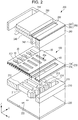
- FIG. 2 is a schematic exploded perspective view of a liquid ejection head 200 according to an embodiment of the invention.
- Fig. 3 is a schematic plan view of the liquid ejection head 200 of the embodiment.
- Fig. 4 is a schematic sectional view of the liquid ejection head 200 of the embodiment taken along line IV-IV in Fig. 3 .
- three directions perpendicular to each other are represented by using an X, a Y, and a Z axis.
- the liquid ejection head according to the present disclosure includes the above-described piezoelectric elements 100 or the actuator 110.
- a liquid ejection head 200 including the piezoelectric elements 100 will be described by way of example.
- the liquid ejection head 200 includes the piezoelectric elements 100, a flow channel substrate 210, a nozzle plate 220, a vibration plate 230, a protective substrate 240, a circuit board 250, and a compliance substrate 260.
- the circuit board 250 and connection wiring lines 204 are omitted for convenience sake.
- the flow channel substrate 210 may be, for example, a silicon substrate.
- the flow channel substrate 210 has a plurality of pressure generating chambers 211.
- the pressure generating chambers 211 are separated by a plurality of partitions 212.
- the flow channel substrate 210 has ink supply ports 213 and communication paths 214 at the end of each pressure generating chamber 211 in the +X axis direction.
- Each ink supply port 213 narrows the corresponding pressure generating chamber 211 in the Y axis direction at the end of the chamber in the +X axis direction to reduce the sectional area of the opening of the chamber.
- the dimension in the Y axis direction of each communication path 214 is, for example, equal to the dimension in the Y axis direction of the pressure generating chamber 211.
- a communicating section 215 is formed adjacent to the communication paths 214 in the +X axis direction. The communicating section 215 defines a part of a manifold 216.
- the manifold 216 acts as a common ink chamber shared by the pressure generating chambers 211.
- the flow channel substrate 210 has therein the liquid flow channels including the pressure generating chambers 211, the ink supply channels 213, the communication paths 214, and the communicating section 215.
- the nozzle plate 220 is disposed on one side (adjacent to the surface in the -Z axis direction) of the flow channel substrate 210.
- the nozzle plate 220 may be made of, for example, SUS (steel use stainless).
- the nozzle plate 220 may be bonded to the flow channel substrate 210 with, for example, an adhesive or a thermal fusion film.
- Nozzle openings 222 are aligned in the Y axis direction in the nozzle plate 220. The nozzle openings 222 communicate with the corresponding pressure generating chambers 211.
- the vibration plate 230 is disposed on one side (adjacent to the surface in the +Z axis direction) of the flow channel substrate 210.
- the vibration plate 230 may include, for example, a first insulating layer 232 disposed on the flow channel substrate 210 and a second insulating layer 234 disposed on the first insulating layer 232.
- the first insulating layer 232 may be made of, for example, silicon oxide.
- the second insulating layer 234 may be made of, for example, zirconium oxide.
- the piezoelectric elements 100 may be arranged, for example, on the vibration plate 230.
- the number of the piezoelectric elements 100 is not particularly limited provided that it is more than one.
- the piezoelectric elements share the second electrode 50 as a common electrode.
- the vibration plate 230 and the first electrodes 10 are displaced by a deformation of the piezoelectric elements 100 capable of electromechanical conversion.
- the vibration plate 230 and the first electrodes 10 effectively act as a vibration plate in the present embodiment.
- only the first electrodes 10 may act as the vibration plate without using the vibration plate 230. If the first electrodes 10 are disposed directly on the flow channel substrate 210, it is beneficial that the first electrodes 10 are protected by a protective film to avoid coming into contact with liquid.
- the first electrodes 10 are discrete electrodes each provided independently for each pressure generating chamber 211.
- the dimension in the Y axis direction of the first electrode 10 is smaller than the dimension in the Y axis direction of the pressure generating chamber 211.
- the dimension in the X axis direction of the first electrode 10 is larger than the dimension in the X axis direction of the pressure generating chamber 211. Both ends in the X axis direction of the first electrode 10 are located outside the pressure generating chamber 211.
- the end of the first electrode 10 on the -X axis direction side is connected to a leading electrode 202.
- the first electrode 10, the first piezoelectric layer 20, the second orientation control layer 30, the second piezoelectric layer 40, and the recess 40a may have any dimensions and any shape, provided that the active portion 101 of the piezoelectric element is located within the pressure generating chamber 211 when viewed from above (see Fig. 3 ).
- the second electrode 50 is a continuous layer disposed over the second piezoelectric layers 40 and the vibration plate 230.
- the second electrode 50 is a common electrode shared by the plurality of piezoelectric elements 100.
- the second electrode 50 has recesses 40a formed by patterning for forming the second piezoelectric layers 40.
- the recesses 40a may be aligned with the pressure generating chambers 211 when viewed from above from the viewpoint of allowing the vibration plate 230 to bend or warp to a greater extent.
- the protective substrate 240 is bonded to the flow channel substrate 210 with an adhesive 203.
- the protective substrate 240 has a through hole 242 therein.
- the through hole 242 passes through the protective substrate 240 in the Z axis direction, thus communicating with the communication section 215.
- the through hole 242 and the communication section 215 define a manifold 216 that will act as a common ink chamber shared by the pressure generating chambers 211.
- the protective substrate 240 also has another through hole 244 passing through the protective substrate 240 in the Z axis direction. One end of each leading electrode 202 is located in the through hole 244.
- the protective substrate 240 has an opening 246 therein.
- the opening 246 is a space that allows the piezoelectric elements 100 to operate without interference.
- the opening 246 may be or may not be sealed.
- the circuit board 250 is disposed on the protective substrate 240.
- the circuit board 250 includes a semiconductor integrated circuit (IC) operable to drive the piezoelectric elements 100.
- the circuit board 250 and the leading electrodes 202 are electrically connected to each other by connection wiring lines 204.
- the compliance substrate 260 is disposed on the protective substrate 240.
- the compliance substrate 260 includes a sealing layer 262 disposed on the protective substrate 240 and a fixing plate 264 disposed on the sealing layer 262.
- the sealing layer 262 seals the manifold 216.
- the sealing layer 262 may be flexible.
- the fixing plate 264 has a through hole 266 therein.
- the through hole 266 passes through the fixing plate 264 in the Z axis direction.
- the through hole 266 is aligned with the manifold 216 when viewed from above (in the Z axis direction).
- the liquid ejection head 200 includes the above-described piezoelectric elements 100, the applied voltage is efficiently used for larger displacement of the vibration plate 230 so that liquid can be efficiently ejected. Also, since the polarized domains of the crystals in the piezoelectric layer are small, pinning is not likely to occur.
- a bias of displacement caused by polarization is reduced, and, for example, changes in volume of the pressure generating chambers 211 can be increased. Consequently, the liquid ejection head 200 can more efficiently eject liquid.
- a substrate 2 was prepared. More specifically, a ⁇ 110 ⁇ silicon substrate was oxidized by heating to yield a 520 nm-thick silicon oxide layer. Subsequently, a zirconium layer was deposited on the silicon oxide layer by sputtering, and the zirconium layer was oxidized by heating to yield a 200 nm-thick zirconium oxide layer. Thus, the substrate 2 was prepared through those steps.
- a 20 nm-thick titanium layer was formed as an adhesion layer on the substrate 2, and a first electrode 10 was formed by forming a 50 nm-thick platinum layer and a 5 nm-thick iridium layer in this order on the titanium adhesion layer.
- a 4 nm-thick titanium layer was formed on the first electrode 10.
- the titanium layer was then subjected to the following operation, and thereby changed into a first orientation control layer 15.
- the degreased precursor layer was further heated at a temperature of 650°C to 800°C and kept at this temperature for a certain period for crystallization (firing step).
- the first orientation control layer 15 and the first piezoelectric layer 20 were formed over the first electrode 10.
- the first piezoelectric layer 20, the first orientation control layer 15, and the first electrode 10 were subjected to patterning so that the patterned first electrodes 10 would act as discrete electrodes for respective piezoelectric elements 100.
- the patterning was performed by ion milling.
- the first piezoelectric layer 20, the first orientation control layer 15, and the first electrode 10, each in a predetermined shape, were completed as shown in Fig. 1 .
- a second orientation control layer 30 was formed.
- the composition of the second orientation control layer 30 is changed by firing the second piezoelectric layer 40.
- a titanium layer was formed as a precursor of the second orientation control layer 30.
- the titanium layer was formed by sputtering.
- the thickness of the titanium layer and the conditions for forming the titanium layer in each Example were as follows.
- titanium layer thickness (nm), argon flow rate (sccm), and sputtering power (W) are shown in this order.
- the degreased precursor layer was further heated at a temperature of 650°C to 800°C and kept at this temperature for a certain period for crystallization (firing step).
- the composition of the titanium layer is changed by the firing operation, and thus the final second orientation control layer 30 has a predetermined composition.
- a series of the steps from the application to the firing was repeated two times so that the resulting piezoelectric body including the first piezoelectric layer 20 had four layers, and thus, the second piezoelectric layer 40 was formed so that the total thickness of the first orientation control layer 15, the first piezoelectric layer 20, the second orientation control layer 30, and the second piezoelectric layer 40 was 760 nm.
- a first layer 51 was first formed. Then, after the first layer 51, the second piezoelectric layer 40, and the second orientation control layer 30 were subjected to patterning, a second layer 52 was formed. More specifically, a 5 nm-thick iridium layer and a 4 nm-thick titanium layer were formed in this order on the second piezoelectric layer 40 by sputtering, thus forming a first layer 51. Subsequently, recovery annealing was performed under the conditions shown below. Then, the first layer 51, the second piezoelectric layer 40, and the second orientation control layer 30 were simultaneously subjected to patterning by ion milling.
- a second layer 52 was formed by forming a 15 nm-thick iridium layer and a 20 nm-thick titanium layer in this order on the first layer 51 by sputtering.
- the second electrode 50 was completed.
- Example 2 The sample of Example 2 was subjected to annealing as Example 5 and Referential Example 2. For each Example, annealing temperature (°C), annealing time (min), and piezoelectric displacement (nm) are shown below in this order.
- Fig. 6 depicts the relationship between the thickness of the titanium layer that will be changed into the second orientation control layer and variation of piezoelectric displacement (Examples 1 to 4 and Referential Example 1).
- the variation of piezoelectric displacement with respect to the displacement in Example 4 in which the thickness of the titanium layer was 4 nm increased toward the thinner side and came to a maximum at the thickness of Example 2 that was 2 nm.
- Fig. 7 depicts the relationship between the thickness of the titanium layer and the thickness of the second orientation control layer after firing.
- the thickness of the titanium layer and the thickness of the second orientation control layer after firing are substantially proportionate to each other, drawing an approximate straight line.
- the thickness of the second orientation control layer corresponding to the thickness of 1.21 nm of the titanium layer is 6.85 nm. Also, the thickness of the second orientation control layer corresponding to the thickness of 4.0 nm of the titanium layer is 21.5 nm.
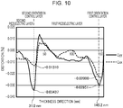
- Figs. 8 and 10 are plots depicting the profile of the crystal distortion in the a-axis direction ((a-axis length/a-axis length of a reference diffraction pattern) - 1: ⁇ xx) of samples of Example 5 and Referential Example 2, respectively, including the first electrode, the first orientation control layer, the first piezoelectric layer, the second orientation control layer, and the second piezoelectric layer and the profile of the crystal distortion in the c-axis direction ((c-axis length/c-axis length of the reference diffraction pattern) - 1: ⁇ yy) of the respective samples.
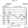
- Figs. 9 and 11 are plots depicting the profile of crystal distortion (c/a) of the samples of Example 5 and Referential Example 2, respectively, including the first electrode, the first orientation control layer, the first piezoelectric layer, the second orientation control layer, and the second piezoelectric layer.
- a substantially parallel electron beam of about 3 nm in diameter was emitted to impinge on a randomly selected (columnar) crystal grain in the second piezoelectric layer on the first electrode in the ⁇ 100> pc direction ( ⁇ DIFF mode, Cs corrector: OFF), and a thus obtained electron diffraction pattern (nano-beam diffraction (NBD) pattern) was synchronized with scan lines to yield a 4D-STEM image (150 nm in width ⁇ 300 nm in height) four-dimensionally distributed in a real space and an inverse space.
- an atomic resolution analytical electron microscope JEM-ARM200F accelerating voltage: 200 kV, manufactured by JEOL
- a camera system ONE-VIEW STEMx system manufactured by GATAN
- Example 5 shown in Fig. 9 and the results of Referential Example 2 shown in Fig. 11 suggest that a large piezoelectric displacement can be produced by aligning the polarization axes in the second orientation control layer, which has a low dielectric constant, parallel to the surface of the first electrode.
- Figs. 9 and 11 suggest that when c/a (ratio of c to a) satisfies 0.980 ⁇ c/a ⁇ 1 (lattice has such a distortion as to lengthen in the plane of the first electrode), piezoelectric displacement increases, and that when 0.985 ⁇ c/a ⁇ 1 holds true, piezoelectric displacement increases with greater reliability.
- the results of analysis show that the composition of the second orientation control layer was changed into titanium-rich lead zirconate titanate (PZT) by a thermal diffusion reaction with the overlying second piezoelectric layer and the thickness thereof increased to about 10 nm (when the titanium layer was formed to a thickness of 2 nm).
- the titanium-rich lead zirconate titanate layer which has a tetragonal nano-domain structure, contributes to 90° domain rotation.
- Figs. 12 and 13 depict section STEM-NBD (nano-beam diffraction) patterns of the first piezoelectric layer (PZT) of Example 5 and Referential Example 2, respectively.
- an atomic resolution analytical electron microscope JEM-ARM200F accelerating voltage: 200 kV, manufactured by JEOL
- a camera system ONE-VIEW STEMx system manufactured by GATAN
- Example 5 the structure of the piezoelectric layer was converted into a fine domain structure having good response to electric field. This is the reason why the piezoelectric layer exhibited a large piezoelectric displacement.
- the expression "a specific member B (herein after referred to as B) disposed over or under a specific member A (hereinafter referred to as A)" includes the case where B is disposed directly on or directly under A and the case where B is disposed on or under A with another member therebetween.
- the expression “B is present over or under A” is independent of the direction of gravity and implies that A and B can be in such a positional relationship by varying the direction in or the angle with which the object is viewed.
Landscapes
- Chemical & Material Sciences (AREA)
- Engineering & Computer Science (AREA)
- Ceramic Engineering (AREA)
- Particle Formation And Scattering Control In Inkjet Printers (AREA)
Abstract
Description
- The present invention relates to a piezoelectric element and a liquid ejection head.
- Typically, a piezoelectric element includes a piezoelectric layer capable of electromechanical conversion, and two electrodes between which the piezoelectric element is disposed. The piezoelectric element may be used, for example, in a liquid ejection head mounted in an ink jet recording apparatus. The piezoelectric layer contains lead zirconate titanate (PZT) or any other compound, and many of the possible materials of the piezoelectric layer have a perovskite crystal structure.
- A thin piezoelectric layer has a structure in which many crystals (crystal grains) are arranged. It has been studied to increase the piezoelectric constant of individual crystals in the thin layer from the viewpoint of increasing the displacement of the piezoelectric layer. For example, in
JP-A-2011-233817 - The piezoelectric properties of a piezoelectric element vary depending on many factors, such as composition, crystal structure, crystal orientation, lattice distortion, domain structure, thickness, and structure at the interface with the electrode. Therefore, merely controlling c/a while focusing on the crystals of the piezoelectric material, as disclosed in the foregoing
JP-A-2011-233817 - According to an aspect of the invention, there is provided a piezoelectric element including a first electrode disposed over a substrate, an orientation control layer disposed over the first electrode and containing titanium, a piezoelectric layer disposed over the orientation control layer and having a perovskite crystal structure, and a second electrode disposed over the piezoelectric layer. The orientation control layer has a thickness in the range of 5.0 nm to 22.0 nm.
- The orientation control layer may have a thickness in the range of 6.85 nm to 21.5 nm.
- The piezoelectric element may further include an additional piezoelectric layer having a perovskite crystal structure between the first electrode and the orientation control layer.
- The total thickness of the piezoelectric layer, the orientation control layer, and the additional piezoelectric layer may be 1.0 µm or less.
- The first electrode may have a thickness in the range of 50 nm to 140 nm.
- The orientation control layer may contain lead and titanium.
- The second electrode may be a common electrode shared with another piezoelectric element.
- According to another aspect of the invention, a liquid ejection head including the piezoelectric element described above is provided.
- Embodiments of the invention will now be described by way of example only with reference to the accompanying drawings, wherein like numbers reference like elements.
-
Fig. 1 is a schematic sectional view of a piezoelectric element according to an embodiment of the invention, including the definition of crystallographic axes. -
Fig. 2 is a schematic exploded perspective view of a liquid ejection head according to an embodiment of the invention. -
Fig. 3 is a schematic plan view of a liquid ejection head according to an embodiment of the invention. -
Fig. 4 is a schematic sectional view of the liquid ejection head shown inFig. 3 , taken along line IV-IV. -
Fig. 5 is a plot of the ratio (V2/V) of the partial voltage V2 applied to a PZT layer to a voltage V applied to a multilayer composite including a low-dielectric-constant layer having a dielectric constant ε1 and the PZT layer (on the assumption that the low-dielectric-constant layer having a capacitance C1 and the PZT layer having a capacitance C2 are coupled in series, wherein the low-dielectric-constant layer has a thickness of 10 nm and the PZT layer has a relative dielectric constant ε2 of 2000 and a thickness of 760 nm). -
Fig. 6 is a plot depicting the relationship between variation of piezoelectric displacement and titanium layer thickness. -
Fig. 7 is a plot depicting the relationship between the thickness of a titanium layer and the thickness of an orientation control layer. -
Fig. 8 is a plot depicting the profile of the crystal distortion in the a-axis direction ((a-axis length/a-axis length of a referential diffraction pattern) -1: εxx) of a sample of Example 5 including a first electrode, a first orientation control layer, a first piezoelectric layer, a second orientation control layer, and a second piezoelectric layer and the profile of the crystal distortion in the c-axis direction ((c-axis length/c-axis length of the referential diffraction pattern) -1: εyy) of the sample. -
Fig. 9 is a plot depicting the profile of crystal distortion (c/a) of the sample of Example 5 including the first electrode, the first orientation control layer, the first piezoelectric layer, the second orientation control layer, and the second piezoelectric layer. -
Fig. 10 is a plot depicting the profile of the crystal distortion in the a-axis direction ((a-axis length/a-axis length of a referential diffraction pattern) -1: εxx) of a sample of Referential Example 2 including a first electrode, a first orientation control layer, a first piezoelectric layer, a second orientation control layer, and a second piezoelectric layer and the profile of the crystal distortion in the c-axis direction ((c-axis length/c-axis length of the referential diffraction pattern) -1: εyy) of the sample. -
Fig. 11 is a plot depicting the profile of crystal distortion (c/a) of the sample of Referential Example 2 including the first electrode, the first orientation control layer, the first piezoelectric layer, the second orientation control layer, and the second piezoelectric layer. -
Fig. 12 is an electron diffraction pattern of PZT crystals in an area of 3 nm in diameter of the sample of Example 5. -
Fig. 13 is an electron diffraction pattern of PZT crystals in an area of 3 nm in diameter of the sample of Referential Example 2. - Some embodiments of the invention will now be described. The following embodiments will be described by way of example. The invention is not limited to the following embodiments, and various modifications may be made within the scope of the invention. All the components disclosed in the following embodiments are not necessarily required for the invention.
- A piezoelectric element disclosed herein will now be described with reference to some of the drawings.
Fig. 1 is a schematic sectional view of apiezoelectric element 100 according to an embodiment of the invention. Thepiezoelectric element 100 includes afirst electrode 10, a firstorientation control layer 15, a firstpiezoelectric layer 20, a secondorientation control layer 30, a secondpiezoelectric layer 40, and asecond electrode 50. - The
first electrode 10 is one of the electrodes operable to apply voltage to the firstorientation control layer 15, the firstpiezoelectric layer 20, the secondorientation control layer 30, and the secondpiezoelectric layer 40. Thefirst electrode 10 may be referred to as the lower electrode. In the embodiment shown inFig. 1 , thefirst electrode 10 is disposed on a substrate 2 (vibration plate 230). - The
first electrode 10 may be in the form of a layer. The thickness of thefirst electrode 10 depends on the size of thepiezoelectric element 100 and, in an embodiment, may be in the range of 3 nm to 300 nm, preferably in the range of 50 nm to 140 nm. For example, in a liquid ejection head in which liquid ejection nozzles are arranged with a high density (for example, 400 dpi or more), smallpiezoelectric elements 100 are densely arranged. In a smallpiezoelectric element 100, as the thickness of thepiezoelectric element 100 becomes smaller, the vibration plate is more efficiently driven. Accordingly, in an embodiment of thepiezoelectric element 100, the total thickness of the firstpiezoelectric layer 20, the secondorientation control layer 30, and the secondpiezoelectric layer 40 may be 1 µm or less. In this instance, the thickness of thefirst electrode 10 may also be reduced in the range of 10 nm to 200 nm, preferably 30 nm to 150 nm or 40 nm to 100 nm. - The
first electrode 10 may contain a platinum group element. Platinum group elements areGroups 8, 9 and 10 elements in the fifth and sixth periods in the periodic table and include ruthenium, rhodium, palladium, osmium, iridium, and platinum. Thefirst electrode 10 may have a multilayer structure including a platinum layer and an iridium layer that are formed in this order from the side opposite the first piezoelectric layer 20 (the side closer to the substrate 2). The iridium layer is a layer containing iridium as a major constituent, and the platinum layer is a layer containing platinum as a major constituent. In the description of the present disclosure, the term "major constituent" of a member or a portion implies that the content of the element of interest accounts for 80% or more (preferably 90% or more, 95% or more, or 98% or more) of the total amount of the elements in the member or portion. - The material of the
first electrode 10 is not particularly limited provided that it is electrically conductive and may be a metal or an electrically conductive oxide. Thefirst electrode 10 may be a multilayer composite defined by a plurality of layers made of such materials. Afirst electrode 10 including a platinum layer and an iridium layer in this order from the side opposite the first piezoelectric layer 20 (the side closer to the substrate 2) can act as a barrier, for example, to hinder more effectively one or more constituents of the firstpiezoelectric layer 20 from penetrating thefirst electrode 10 and diffusing. - In the embodiment shown in
Fig. 1 , thefirst electrode 10 is a discrete electrode separating the active portion 101 of apiezoelectric element 100 from the active portions of the other piezoelectric elements. In this instance, the active portion 101 is the overlap between thefirst electrode 10 and thesecond electrode 50 when viewed from above. In the description of the present disclosure, the portion of thepiezoelectric element 100 other than the active portion 101 is referred to as the inactive portion. - The first
orientation control layer 15 is disposed over thefirst electrode 10. In the embodiment shown inFig. 1 , the firstorientation control layer 15 is disposed on thefirst electrode 10. Also, the firstorientation control layer 15 lies between thefirst electrode 10 and the firstpiezoelectric layer 20. The firstorientation control layer 15 controls the orientation of the crystals in the firstpiezoelectric layer 20. - The thickness of the first
orientation control layer 15 may be in the range of 1.0 nm to 30.0 nm and is preferably 2.0 nm to 20.0 nm. - The first
orientation control layer 15 is made of a material containing titanium. The material of the firstorientation control layer 15 may be lead titanate or a solid solution made by substituting another element (for example, zirconium) for the titanium or the lead of lead titanate. For example, the firstorientation control layer 15 may be formed by depositing a titanium layer by sputtering and firing the titanium layer simultaneously with a precursor of the firstpiezoelectric layer 20 when the firstpiezoelectric layer 20 is formed. This firing changes the titanium layer into a layer containing mainly lead titanate. The layer thus prepared may be used as the firstorientation control layer 15. - The first
piezoelectric layer 20 is disposed over thefirst electrode layer 10. In the embodiment shown inFig. 1 , the firstpiezoelectric layer 20 is disposed on the firstorientation control layer 15. Also, the firstpiezoelectric layer 20 lies between thefirst electrode 10 and the secondorientation control layer 30. - The thickness of the first
piezoelectric layer 20 may be, for example, in the range of 100 nm to 300 nm. In an embodiment of thepiezoelectric element 100 that is used in a liquid ejection head in which liquid ejection nozzles are arranged with a density as high as 400 dpi or more, the firstpiezoelectric layer 20 may have, for example, as small a thickness as 50 nm to 200 nm. The firstpiezoelectric layer 20 may be deformed by applying a voltage (electric field) between thefirst electrode 10 and thesecond electrode 50. The firstpiezoelectric layer 20 contains crystals having a perovskite crystal structure and produces an electromechanical conversion effect when a voltage is applied thereto. - The first
piezoelectric layer 20 may contain a substance having piezoelectric properties, for example a composite oxide having a perovskite crystal structure. Examples of the metal elements that may be contained in the firstpiezoelectric layer 20 include Pb, Ba, Ca, Nb, La, Li, Sr, Bi, Na, K, Fe, Ti, Ta, Mg, Mo, Ni, Mn, Zr, Zn, W, and Yb. - Among compounds containing these metal elements, lead zirconate titanate (PZT) containing Ti, Zr, and Pb, a composite oxide (KNN) containing potassium (K), sodium (Na), and niobium (Nb), bismuth ferrate (BFO) containing Bi and Fe, or lead zirconate titanate niobate (Pb(Zr,Ti,Nb)O3: PZTN) may be used. Such a composite oxide is likely to exhibit favorable piezoelectric properties.
- In the embodiment shown in
Fig. 1 , the firstpiezoelectric layer 20 is formed into a shape corresponding to the shape of thefirst electrode 10 by patterning. Therefore, the portion of the firstpiezoelectric layer 20 lying under thesecond electrode 50 is located in the active portion 101. - The first
piezoelectric layer 20 is defined by a mass of a large number of crystals (crystal grains) and is composed of preferentially {100}-oriented crystals. The phrase "preferentially {100}-oriented" means that all the crystals or almost all (50% or more, preferably 80% or more or 90% or more) the crystals in the piezoelectric layer are oriented in the {100} plane. The {100} plane includes a plurality of planes equivalent to the (100) plane. - For the crystal axes of the crystals in the first
orientation control layer 15, the firstpiezoelectric layer 20, the secondorientation control layer 30, and the secondpiezoelectric layer 40, the c-axis extends in the direction normal to the surface of thefirst electrode 10 and the a-axis extends in the direction parallel to the surface of thefirst electrode 10, as shown inFig. 1 . In the embodiment shown inFig. 1 , the a-axis may extend in any direction rotated on the c-axis. - Since the crystals in the first
piezoelectric layer 20 are oriented in the {100} plane, thepiezoelectric element 100 has piezoelectric properties. The crystals in the firstpiezoelectric layer 20 are preferentially oriented in the {100} plane by an operation of the firstorientation control layer 15. - The crystals in the first
piezoelectric layer 20 each include polarized domains. A monocrystalline grain has areas having different polarization directions. A polarized domain refers to an area of such areas where the polarization directions are aligned. In general, when a piezoelectric material is crystallized (fired), many polarized domains having different spontaneous polarization directions are formed in a crystal. The polarized domains are formed depending on the process of crystal growth, presence of crystal defects, recovery from crystal defects (heat treatment), and combinations of chemical elements in the piezoelectric material, but it is not clear how the polarized domains are formed. - If a perovskite crystal structure is polarized, the crystal lattice is distorted and the crystals become tetragonal, rhombohedral, or less symmetrical than rhombohedral according to the polarization direction. Accordingly, the lattice constant of a crystal varies according to the polarization direction. Therefore, while the lattice constant of one polarized domain is constant, another polarized domain polarized in a different direction has a different lattice constant according to the polarization direction.
- The first
piezoelectric layer 20 disclosed herein contains densely arranged stacking defects in an area of 3 nm or less in diameter. If the domain size is reduced due to the stacking defects, domain walls become dense. Accordingly, the relative dielectric constant increases and the response to electric field is enhanced. Also, the firstpiezoelectric layer 20 contains a variety of ions having different charges and ionic radiuses. Different charges cause local electric fields, and different ionic radiuses produce stresses. The domains are fixed by such local electric fields or stresses. It is thought that the first piezoelectric layer thus comes into a state having no hysteresis, that is, into a state having a relative dielectric constant independent of electric field. Whether stacking defects are present in or absent from such a very small area can be checked by, for example, nano-beam electron diffraction using a transmission electron microscope, which will be described later herein. - In the first
piezoelectric layer 20 of thepiezoelectric element 100 disclosed herein, subdivided nano-domains are present which contain stacking defects in an area of less than 3 nm in diameter to relieve structural distortion in the crystal grain. This causes a new dielectric polarization, enhancing response to electric field and facilitating domain rotation. - The second
orientation control layer 30 is disposed over the firstpiezoelectric layer 20. The secondorientation control layer 30 controls the orientation of the crystals in the secondpiezoelectric layer 40. Therefore, the secondorientation control layer 30 is disposed under the secondpiezoelectric layer 40. The secondorientation control layer 30 may be disposed in the inactive portion as well as in the active portion 101. - In the embodiment shown in
Fig. 1 , the secondorientation control layer 30 covers the firstpiezoelectric layer 20, the firstorientation control layer 15, thefirst electrode 10, and thesubstrate 2. In thepiezoelectric element 100 disclosed herein, the structure under the secondorientation control layer 30 is patterned so that thefirst electrode 10 can be a discrete electrode. Therefore, the surface of the firstpiezoelectric layer 20, the sides of the firstpiezoelectric layer 20, the firstorientation control layer 15 and thefirst electrode 10, and the surface of thesubstrate 2 are exposed by the patterning. The secondorientation control layer 30 is formed on the structure in such a state. Thus, the orientation of the secondpiezoelectric layer 40 over theinactive portion 40 is increased, reducing cracks in the secondpiezoelectric layer 40. - The second
orientation control layer 30 is made of a material containing titanium. The material of the secondorientation control layer 30 may be lead titanate or a solid solution made by substituting another element (for example, zirconium) for the titanium or the lead of lead titanate. For example, the secondorientation control layer 30 may be formed by depositing a titanium layer by sputtering and firing the titanium layer simultaneously with a precursor of the secondpiezoelectric layer 40 when the secondpiezoelectric layer 40 is formed. This firing changes the titanium layer into a layer containing mainly lead titanate. The layer thus prepared may be used as the secondorientation control layer 30. - The dielectric constant of the second
orientation control layer 30 may be reduced depending on the material. For example, the relative dielectric constant of lead titanate is about 100 to 300 and is much lower than the relative dielectric constant (about 1500) of piezoelectric materials, such as lead zirconate titanate (PZT). Accordingly, a large part of the voltage (partial voltage) applied between thefirst electrode 10 and thesecond electrode 50 concentrates on the secondorientation control layer 30 disposed between thefirst electrode 10 and thesecond electrode 50. Consequently, the voltage (partial voltage) applied to the firstpiezoelectric layer 20 and the secondpiezoelectric layer 40 is relatively reduced. This may reduce the displacement of thepiezoelectric element 100 with respect to applied voltage. From such a viewpoint, it is beneficial that the material of the secondorientation control layer 30 has a higher relative dielectric constant and that the secondorientation control layer 30 has a smaller thickness. - Thus, by selecting a material having a higher relative dielectric constant for the second
orientation control layer 30, the displacement of thepiezoelectric element 100 can be increased. In addition, if the secondorientation control layer 30 contains a specific material such as lead titanate, the relative dielectric constant can be adjusted by controlling distortion of the crystals of the specific material. A secondorientation control layer 30 made of lead titanate allows continuous crystal growth of the underlying firstpiezoelectric layer 20 and the overlying secondpiezoelectric layer 40 that have different compositions. In other words, the firstpiezoelectric layer 20, the secondorientation control layer 30, and the secondpiezoelectric layer 40 are epitaxially crystallized. Thus, the relative dielectric constant of the secondorientation control layer 30 can be controlled by controlling the crystal distortion of the secondorientation control layer 30. - In the
piezoelectric element 100 disclosed herein, the lattice distortion (c/a) of the crystals in the secondorientation control layer 30 is 0.980 to less than 1.000. Hence, the lattice of the crystals in the secondorientation control layer 30 have a shape crushed in the c-axis direction (elongating in the a-axis and b-axis directions). Thus, the secondorientation control layer 30 is polarized in the direction parallel to the surface of the first electrode 10 (a-axis). - According to Landolt Bornstein's Data Book, the relative dielectric constant ε of PbTiO3 in a tetragonal system is the minimum (ε: about 100) in the polarization axis direction and the maximum (ε: about 200) in the direction perpendicular to the polarization axis. Therefore, by aligning the polarization axes parallel to the in-plane direction (a-axis), the orientation control layer has a larger dielectric constant, increasing the relative dielectric constant in the thickness direction compared to the case where the polarization axes are oriented in the thickness direction (c-axis) perpendicular to the in-plane direction. This alignment therefore increases the relative dielectric constant in the c-axis direction. Thus, the relative dielectric constant of the second
orientation control layer 30 made of lead titanate can be increased up to about 200. Since the relative dielectric constant is thus increased in the thickness direction, the effective electric field applied to the entire PZT layer can be increased. - If the lattice distortion (c/a) of the second
orientation control layer 30 is less than 0.980, the distortion of the tetragonal lattice becomes excessive, and a large energy is required for domain rotation. If domains are forcibly rotated, cracks are likely to occur. The lattice distortion has a suitable range. -
Fig. 5 depicts a plot of the ratio (V2/V) of partial voltage V2 applied to a PZT layer to voltage V applied to a multilayer composite including a low-dielectric-constant layer having a dielectric constant ε1 and the PZT layer. As shown inFig. 5 , by increasing the dielectric constant ε1 of the low-dielectric-constant layer, the partial voltage (V2/V) applied to the PZT layer is increased and, thus, the efficiency of the displacement of the piezoelectric element can be increased. - Also, since the second
orientation control layer 30 is disposed between thefirst electrode 10 and thesecond electrode 50, it is beneficial to reduce the thickness of the secondorientation control layer 30 from the viewpoint of minimizing the partial voltage. However, a secondorientation control layer 30 having an excessively small thickness does not function to sufficiently control the crystal orientation of the inactive portion of the secondpiezoelectric layer 40. The thickness of the secondorientation control layer 30 therefore has a suitable range over which it is most effective. The suitable thickness of the secondorientation control layer 30 varies depending on the material of the secondorientation control layer 30, the material of the secondpiezoelectric layer 40, the size of thepiezoelectric element 100, the distance between thefirst electrode 10 and the second electrode 50 (the total thickness of the firstorientation control layer 15, the firstpiezoelectric layer 20, the secondorientation control layer 30, and the second piezoelectric layer 40), and other factors. - In the
piezoelectric element 100 disclosed therein, the thickness of the secondorientation control layer 30 is in the range of 5.0 nm to 22.0 nm and is preferably in the range of 6.0 nm to 21.5 nm, more preferably 6.8 nm to 21.3 nm, for example, 7.0 nm to 20.0 nm or 7.0 nm to 19.0 nm. When the thickness of the secondorientation control layer 30 is in such a range, domains can be 90° rotated easily and efficiently, in the direction in which voltage is applied, from the state where the polarization axes of the tetragonal crystals lean in the a-axis direction. In addition, since the energy for domain rotation is reduced, cracks are also reduced. Thus, the secondorientation control layer 30 can give a distortion corresponding to the c/a ratio to thepiezoelectric element 100 to increase the magnitude of displacement, as well as appropriately controlling the crystal orientation of the secondpiezoelectric layer 40, even though the relative dielectric constant of the secondorientation control layer 30 is low. In addition, a secondorientation control layer 30 having a thickness in the above range is particularly beneficial for the case where the total thickness of the firstorientation control layer 15, the firstpiezoelectric layer 20, the secondorientation control layer 30, and the secondpiezoelectric layer 40 is 1 µm or less. - When the second
orientation control layer 30 is made of lead titanate, it may be formed by depositing a titanium layer by sputtering and firing the titanium layer simultaneously with a precursor of the secondpiezoelectric layer 40. In this instance, the thickness of the secondorientation control layer 30 may be varied by, for example, controlling the thickness of the titanium layer. In this instance, also, a calibration curve of the relationship between the thickness of the titanium layer and the thickness of the final secondorientation control layer 30 is prepared in advance, and a secondorientation control layer 30 having a predetermined thickness may be formed according to the calibration curve (as in the Examples). - If the second
piezoelectric layer 40 is formed through a plurality of steps (as described later herein), the secondorientation control layer 30 is subjected to heat cycles many times by drying, degreasing, and firing. - The thickness of the second
orientation control layer 30 may be measured by, for example, using a transmission electron microscope and an optional analytical device. - The second
piezoelectric layer 40 is disposed over the secondorientation control layer 30. In the embodiment shown inFig. 1 , the secondpiezoelectric layer 40 is disposed on the secondorientation control layer 30 and in the active portion 101 and the inactive portion of thepiezoelectric element 100. In the preset disclosure, when the secondpiezoelectric layer 40 is called a/the piezoelectric layer, the firstpiezoelectric layer 20 is called an additional piezoelectric layer. - The thickness of the second
piezoelectric layer 40 may be, for example, in the range of 400 nm to 900 nm. In an embodiment of thepiezoelectric element 100 that is used in a liquid ejection head in which liquid ejection nozzles are arranged with a density as high as 400 dpi or more, the secondpiezoelectric layer 40 may have a smaller thickness, for example, in the range of 300 nm to 700 nm. The secondpiezoelectric layer 40 may be deformed by applying a voltage (electric field) between thefirst electrode 10 and thesecond electrode 50. The secondpiezoelectric layer 40 contains crystals having a perovskite crystal structure and produces an electromechanical conversion effect when a voltage is applied thereto. - The second
piezoelectric layer 40 may contain a substance having piezoelectric properties, for example a composite oxide having a perovskite crystal structure. Examples of the metal elements that may be contained in the secondpiezoelectric layer 40 include Pb, Ba, Ca, Nb, La, Li, Sr, Bi, Na, K, Fe, Ti, Ta, Mg, Mo, Ni, Mn, Zr, Zn, W, and Yb. - Among compounds containing these metal elements, lead zirconate titanate (PZT) containing Ti, Zr, and Pb, a composite oxide (KNN) containing potassium (K), sodium (Na), and niobium (Nb), bismuth ferrate (BFO) containing Bi and Fe, or lead zirconate titanate niobate (Pb(Zr,Ti,Nb)O3: PZTN) may be used. Such a composite oxide is likely to exhibit favorable piezoelectric properties.
- In the embodiment shown in
Figs. 1 and2 , the secondpiezoelectric layer 40 is formed by patterning. The portions removed from the secondpiezoelectric layer 40 by patterning form recesses 40a. The active portion 101 of thepiezoelectric element 100 is the overlap between thefirst electrode 10 and thesecond electrode 50. The secondpiezoelectric layer 40 may be formed by performing a series of some steps once or a plurality of times. The secondpiezoelectric layer 40 in the embodiment shown inFig. 1 is formed through many steps. The broken lines in the secondpiezoelectric layer 40 shown inFig. 1 suggest that the secondpiezoelectric layer 40 is formed by performing a set of steps of coating (application) and firing three times. The broken lines in the figure do not represent boundaries between portions having structural variations, and the layers divided by the broken lines form a continuous structure. Such layers may have variations in composition. - The second
piezoelectric layer 40 is defined by a mass of a large number of crystals (crystal grains) as with the firstpiezoelectric layer 20, and the c-axes of the crystals extend substantially parallel to the normal of the first electrode 10 (in the direction toward thesecond electrode 50 from the first electrode 10). - The second
piezoelectric layer 40 in which the crystals are preferentially oriented in the {100} plane can exhibit favorable piezoelectric properties. The presence of the above-described secondorientation control layer 30 allows the crystals in the secondpiezoelectric layer 40 to be oriented in the [001] direction. The firstpiezoelectric layer 20, the secondorientation control layer 30, and the secondpiezoelectric layer 40 are stacked and the crystals in these layers may form a continuous structure. - The crystals in the second
piezoelectric layer 40 each include polarized domains as in the case of the firstpiezoelectric layer 20. - The domain size of the crystals in the second
piezoelectric layer 40 of the piezoelectric element disclosed herein may be, but is not limited to, 10 nm or less or 5 nm or less. The reason why the polarized domain size of the crystals in the secondpiezoelectric layer 40 is larger than the polarized domain size of the crystals in the firstpiezoelectric layer 20 is that the secondpiezoelectric layer 40 has more favorable crystallinity than the firstpiezoelectric layer 20. This is because the diffusion toward the first electrode of lead due to heat cycles is reduced as the piezoelectric layer concerned is located higher up the stack of layers starting from the first elecrode, and hence the defects of lead in the A site of the perovskite skeleton are reduced in the second piezoelectric layer relative to the first. Thus, such a second piezoelectric layer allows easy polarization rotation independent of the size of polarized domains, and pinning becomes unlikely to occur. - The second
piezoelectric layer 40 may be formed by, for example, a sol-gel method and may have a multilayer structure as described above. More specifically, the secondpiezoelectric layer 40 may be formed by repeating a set of steps including at least two of the steps of application of raw material, drying, degreasing, and firing several times. - The
second electrode 50 is disposed over the secondpiezoelectric layer 40. Thesecond electrode 50 includes afirst layer 51 and asecond layer 52. In the embodiment shown inFig. 1 , thefirst layer 51 of thesecond electrode 50 is disposed on the secondpiezoelectric layer 40 and is formed by patterning as in the case of the secondpiezoelectric layer 40. Thesecond layer 52 of thesecond electrode 50 lies on thefirst layer 51 on the secondpiezoelectric layer 40 and within therecesses 40a formed by etching the secondpiezoelectric layer 40. Thesecond electrode 50 is an electrode operable to apply voltage to the firstorientation control layer 15, the firstpiezoelectric layer 20, the secondorientation control layer 30, and the secondpiezoelectric layer 40. Thesecond electrode 50 may be referred to as the upper electrode. - Both the
first layer 51 and thesecond layer 52 of thesecond electrode 50 may be in the form of a layer. The thickness of the first layer of thesecond electrode 51 may be, for example, in the range of 2 nm to 20 nm. The thickness of the second layer of thesecond electrode 52 may be, for example, in the range of 5 nm to 50 nm. - The
second electrode 50 may be made of a metal such as iridium, platinum, or titanium; an electrically conductive oxide of those metals, such as iridium oxide; strontium ruthenate; or any other material. Thesecond electrode 50 may be a multilayer composite defined by some sets of the above-described layers. For example, thefirst layer 51 of thesecond electrode 50 may have a multilayer structure including an iridium layer and a titanium layer deposited in this order from the secondpiezoelectric layer 40 side (the side closer to the first electrode 10). Similarly, thesecond layer 52 of thesecond electrode 50 may have a multilayer structure including an iridium layer and a titanium layer deposited in this order from the secondpiezoelectric layer 40 side. The iridium layer is a layer containing iridium as a major constituent, and the titanium layer is a layer containing titanium as a major constituent. In thefirst layer 51, in this instance, the thickness of the iridium layer may be in the range of 3 nm to 7 nm, and the thickness of the titanium layer may be in the range of 2 nm to 6 nm. In thesecond layer 52, also, the thickness of the iridium layer may be in the range of 10 nm to 20 nm, and the thickness of the titanium layer may be in the range of 15 nm to 25 nm. - Such a structure of the
second electrode 50, which includes thefirst layer 51 and thesecond layer 52 that form a multilayer structure including an iridium layer, a titanium layer, an iridium layer, and a titanium layer in this order on the secondpiezoelectric layer 40, increases the Schottky barrier at the interface with thesecond electrode 50 by recovery annealing after the formation of thesecond electrode 50, thus reducing leakage current at the interface. In addition, such a structure absorbs excess lead effectively. - The
piezoelectric element 100 may be disposed on asubstrate 2. Thesubstrate 2 is a flat plate made of, for example, a semiconductor or an insulating material. Thesubstrate 2 may be composed of a single layer or a plurality of layers. Thesubstrate 2 may have any internal structure provided that the upper surface is flat. For example, thesubstrate 2 may a hollow plate. - The
substrate 2 may be aflexible vibration plate 230 that can be deformed (displaced) by the operation of thepiezoelectric element 100 or a more sophisticated structure including thevibration plate 230. Thevibration plate 230 may be defined by, for example, a silicon oxide layer, a zirconium oxide layer, or a multilayer composite including such layers (for example, a multilayer composite including a silicon oxide layer and a zirconium oxide layer on the silicon oxide layer). An adhesion layer (not shown) may be disposed between thefirst electrode 10 and thesubstrate 2 so as to enhance the adhesion therebetween. The adhesion layer may be, for example, a titanium layer, a titanium oxide layer, or a zirconium layer. If the adhesion layer is an electrically conductive layer, such as a titanium layer or a zirconium layer, the electrically conductive adhesion layer may be considered to be a part of thefirst electrode 10. - In the present disclosure, the structure constituted of the substrate 2 (vibration plate 230) and the
piezoelectric element 100 may be referred to as anactuator 110 in some cases. When thepiezoelectric element 100 is deformed, theactuator 110 bends or vibrates. In a structure in which thevibration plate 230 of theactuator 110 defines a part of the wall of the pressure generating chamber of a liquid ejection head described later herein, thevibration plate 230 enables the capacity of the pressure generating chamber to vary according to the input signal. - The
actuator 110 may be used, for example, as a piezoelectric actuator operable to apply a pressure to the liquid in the pressure generating chamber in a liquid ejection head or a printer including the liquid ejection head. Thepiezoelectric element 100 may be used as a piezoelectric sensor operable to detect a deformation of the piezoelectric layer as an electrical signal (such as a supersonic sensor or a gyroscopic sensor). - In order to determine the axial lengths of crystals and the size of polarized domains, the lattice distortion of the crystals is accurately measured. A progression in technology of scanning transmission electron microscopes (STEM) with spherical aberration correction and peripheral devices, such as CMOS cameras, enables nano-size regions to be irradiated with a parallel electron beam. Also, a structural analysis method using section STEM-NBD (nano-beam diffraction) that enables electron diffraction patterns of very small spots synchronized with scan lines to be rapidly obtained has been established. This method enables lattice distortion at interfaces, of which the detection has been difficult, to be detected with a sensitivity of 0.1% (1/1000) or less.
- For such analysis, an atomic resolution analytical electron microscope JEM-ARM200F (accelerating voltage: 200 kV, manufactured by JEOL) and ONE-VIEW STEMx camera system (manufactured by GATAN) may be used.
- More specifically, for analysis of the crystals in the second
orientation control layer 30, a substantially parallel electron beam of about 3 nm in diameter is emitted to impinge on a randomly selected (columnar) crystal grain in the <100> pc direction (µµDIFF mode, Cs corrector: OFF), and a thus obtained electron diffraction pattern (nano-beam diffraction (NBD) pattern) is synchronized with scan lines to yield a 4D-STEM image (150 nm in width × 300 nm in height) four-dimensionally distributed in a real space and an inverse space. - For the distortion ratio (c/a) of the crystal, the distortion at each point is automatically measured with respect to a referential diffraction pattern of the interior of the crystal grain, and a distortion map image is displayed. Still more specifically, the distortion in the direction parallel to the first electrode 10 ((a-axial length/a-axial length in the referential diffraction pattern) -1: εxx) and the distortion in the direction perpendicular to the first electrode 10 ((c-axial length/c-axial length in the referential diffraction pattern) - 1: εyy) may be measured. The two distortions in each direction are converted to the respective axial lengths (1 + εxx, 1 + εyy), and the map image of their ratio c/a is displayed. The distortion ratio (c/a) is read from the map image.
- The crystallinity of each of the piezoelectric layers may also be determined from an electron diffraction pattern (nano-beam diffraction pattern). An electron diffraction pattern of a monocrystalline region reflects the crystallinity of the region defined by the spot diameter of the convergent electron beam. If the crystal of a diffraction pattern has a defect, a spot or a streak derived from the defect is observed in the diffraction pattern.
- In the
piezoelectric element 100 disclosed herein, since the thickness of the secondorientation control layer 30 is in the range of 5.0 nm to 22.0 nm, the displacement of the entirepiezoelectric element 100 can be large even if the partial voltage applied to the secondorientation control layer 30 of the voltage applied between thefirst electrode 10 and thesecond electrode 50 is high. In thepiezoelectric element 100 disclosed herein, in addition, since the distortion ratio (c/a) of crystals in the secondorientation control layer 30 is in the range of 0.980 to less than 1.000, the relative dielectric constant of the secondorientation control layer 30 is increased, and consequently, the displacement of the entirepiezoelectric element 100 can be large even if the partial voltage applied to the secondorientation control layer 30 of the voltage applied between thefirst electrode 10 and thesecond electrode 50 is high. Furthermore, in the firstpiezoelectric layer 20 of thepiezoelectric element 100, since the domains are subdivided by stacking defects in an area having a diameter of 3 nm or less, it is thought that the response to electric field of the first piezoelectric layer is enhanced. Since domains can be rotated in a low electric field, the firstpiezoelectric layer 20 is unlikely to crack. - A method for manufacturing the
piezoelectric element 100 disclosed herein will now be described. - First, a
substrate 2 is prepared. More specifically, a {110} silicon substrate is oxidized by heating to yield a 520 nm-thick silicon oxide layer. Subsequently, a zirconium layer is deposited on the silicon oxide layer by sputtering, and the zirconium layer is oxidized by heating to yield a 200 nm-thick zirconium oxide layer. Thus, thesubstrate 2 is prepared through those steps. - Next, a 20 nm-thick titanium layer is formed as an adhesion layer on the
substrate 2, and afirst electrode 10 is formed by forming a 50 nm-thick platinum layer and a 5 nm-thick iridium layer in this order on the titanium adhesion layer. Although the thickness of thefirst electrode 10 may be varied from the thickness in this state by firing described below or any other operation, the thickness is adjusted in this step of sputtering so that the final thickness can be in the range of 10 nm to 200 nm. - Next, a first
orientation control layer 15 is formed. The composition of the firstorientation control layer 15 will be changed by firing the firstpiezoelectric layer 20 or the secondpiezoelectric layer 40. In this step, a 4 nm-thick titanium layer is formed as a precursor of the firstorientation control layer 15. The titanium layer may be formed by, for example, sputtering. As described above, the thickness of the titanium layer may be adjusted so that the final firstorientation control layer 15 can have a thickness in the range of 1.0 nm to 50.0 nm. - Subsequently, a first
piezoelectric layer 20 is formed on the titanium layer by a liquid-phase process. A precursor solution that is a sol having, for example, a composition: lead/zirconium/titanium = 120/52/48 is applied onto the titanium layer by spin coating or the like to form a precursor layer (application step). The precursor layer is heated at a temperature of 130°C to 250°C for a certain period for drying (drying step), and the dried precursor layer is further heated to a temperature of 300°C to 450°C and kept at this temperature for a certain period for degreasing (degreasing step). The degreased precursor layer is further heated at a temperature of 650°C to 800°C and kept at this temperature for a certain period for crystallization (firing step). Thus, the firstpiezoelectric layer 20 is formed over thefirst electrode 10. Also, the firstorientation control layer 15 is completed through the steps described above. - Subsequently, the first
piezoelectric layer 20, the firstorientation control layer 15, and thefirst electrode 10 are subjected to patterning so that the patternedfirst electrodes 10 can act as discrete electrodes for respectivepiezoelectric elements 100. The patterning may be performed by, for example, ion milling. Thus, the firstpiezoelectric layer 20, the firstorientation control layer 15, and thefirst electrode 10, each in a predetermined shape, are completed as shown inFig. 1 . - Next, a second
orientation control layer 30 is formed. The composition of the secondorientation control layer 30 will be changed by firing the secondpiezoelectric layer 40. In this step, a titanium layer is formed as a precursor of the secondorientation control layer 30. The titanium layer may be formed by, for example, sputtering. The thickness of the titanium layer is, for example, in the range of 1.0 nm to 5.0 nm and, as described above, it may be adjusted so that the final secondorientation control layer 30 can have a thickness in the range of 5.0 nm to 22.0 nm. - Subsequently, a second
piezoelectric layer 40 is formed on the titanium layer by a liquid-phase process. A precursor solution that is a sol having a composition: lead/zirconium/titanium = 120/52/48 is applied onto the titanium layer by spin coating to form a precursor layer (application step). The precursor layer is heated at a temperature of 130°C to 250°C for a certain period for drying (drying step), and the dried precursor layer is further heated to a temperature of 300°C to 450°C and kept at this temperature for a certain period for degreasing (degreasing step). The degreased precursor layer is further heated at a temperature of 650°C to 800°C and kept at this temperature for a certain period for crystallization (firing step). The composition of the titanium layer is changed by the firing operation, and thus the final secondorientation control layer 30 has a predetermined composition. In the embodiment shown inFig. 1 , a series of steps from application to firing is repeated two times (performed three times in total), thus forming the secondpiezoelectric layer 40 defined by three layers. Thus, the secondorientation control layer 30 is completed, and the secondpiezoelectric layer 40 is formed on the secondorientation control layer 30. - For the drying, degreasing and firing steps for forming the first
piezoelectric layer 20 and the secondpiezoelectric layer 40, a rapid thermal annealing (RTA) apparatus using an infrared lamp may be used as a heating apparatus. - Next, a
second electrode 50 is formed on the secondpiezoelectric layer 40. For forming thesecond electrode 50, afirst layer 51 is first formed. Then, after thefirst layer 51, the secondpiezoelectric layer 40, and the secondorientation control layer 30 are subjected to patterning, asecond layer 52 is formed. - For forming the
first layer 51, for example, a 5 nm-thick iridium layer and a 4 nm-thick titanium layer are formed in this order on the secondpiezoelectric layer 40 by sputtering. In this state, heat treatment (recovery annealing) may be performed, if necessary, to repair defects in the piezoelectric layer caused by sputtering. The recovery annealing may be performed at a temperature of, for example, 650°C to 800°C. - After the formation of the
first layer 51, thefirst layer 51, the secondpiezoelectric layer 40, and the secondorientation control layer 30 are subjected to patterning at one time by, for example, ion milling. In this step, recesses 40a are formed in the secondpiezoelectric layer 40, so that the substrate 2 (zirconium layer), the side surface of the secondorientation control layer 30, the side surface of the secondpiezoelectric layer 40, and thefirst layer 51 are exposed in each recess. - Then, a
second layer 52 is formed by, for example, forming a 15 nm-thick iridium layer and a 20 nm-thick titanium layer in this order on thefirst layer 51 by sputtering. Thus, thesecond electrode 50 is completed as a common electrode. - Through the above steps, the
piezoelectric element 100 is completed. If thesubstrate 2 is avibration plate 230 or if thesubstrate 2 is worked into avibration plate 230, anactuator 110 may be produced by an additional step performed on thesubstrate 2 or thevibration plate 230. Although in the method described above, the piezoelectric layers are formed by a liquid-phase process, the piezoelectric layers may be formed by, for example, CVD, sputtering, or any other method without particular limitation. - A liquid ejection head according to an embodiment of the invention will now be described with reference to some drawings.
Fig. 2 is a schematic exploded perspective view of aliquid ejection head 200 according to an embodiment of the invention.Fig. 3 is a schematic plan view of theliquid ejection head 200 of the embodiment.Fig. 4 is a schematic sectional view of theliquid ejection head 200 of the embodiment taken along line IV-IV inFig. 3 . InFigs. 2 to 4 , three directions perpendicular to each other are represented by using an X, a Y, and a Z axis. - The liquid ejection head according to the present disclosure includes the above-described
piezoelectric elements 100 or theactuator 110. In the following description, aliquid ejection head 200 including thepiezoelectric elements 100 will be described by way of example. - As shown in
Figs. 2 to 4 , theliquid ejection head 200 includes thepiezoelectric elements 100, aflow channel substrate 210, anozzle plate 220, avibration plate 230, aprotective substrate 240, acircuit board 250, and acompliance substrate 260. InFig. 3 , thecircuit board 250 andconnection wiring lines 204 are omitted for convenience sake. - The
flow channel substrate 210 may be, for example, a silicon substrate. Theflow channel substrate 210 has a plurality ofpressure generating chambers 211. Thepressure generating chambers 211 are separated by a plurality ofpartitions 212. - The
flow channel substrate 210 hasink supply ports 213 andcommunication paths 214 at the end of eachpressure generating chamber 211 in the +X axis direction. Eachink supply port 213 narrows the correspondingpressure generating chamber 211 in the Y axis direction at the end of the chamber in the +X axis direction to reduce the sectional area of the opening of the chamber. The dimension in the Y axis direction of eachcommunication path 214 is, for example, equal to the dimension in the Y axis direction of thepressure generating chamber 211. A communicatingsection 215 is formed adjacent to thecommunication paths 214 in the +X axis direction. The communicatingsection 215 defines a part of amanifold 216. The manifold 216 acts as a common ink chamber shared by thepressure generating chambers 211. Thus, theflow channel substrate 210 has therein the liquid flow channels including thepressure generating chambers 211, theink supply channels 213, thecommunication paths 214, and the communicatingsection 215. - The
nozzle plate 220 is disposed on one side (adjacent to the surface in the -Z axis direction) of theflow channel substrate 210. Thenozzle plate 220 may be made of, for example, SUS (steel use stainless). Thenozzle plate 220 may be bonded to theflow channel substrate 210 with, for example, an adhesive or a thermal fusion film.Nozzle openings 222 are aligned in the Y axis direction in thenozzle plate 220. Thenozzle openings 222 communicate with the correspondingpressure generating chambers 211. - The
vibration plate 230 is disposed on one side (adjacent to the surface in the +Z axis direction) of theflow channel substrate 210. Thevibration plate 230 may include, for example, a first insulatinglayer 232 disposed on theflow channel substrate 210 and a second insulatinglayer 234 disposed on the first insulatinglayer 232. The first insulatinglayer 232 may be made of, for example, silicon oxide. The secondinsulating layer 234 may be made of, for example, zirconium oxide. - The
piezoelectric elements 100 may be arranged, for example, on thevibration plate 230. The number of thepiezoelectric elements 100 is not particularly limited provided that it is more than one. In the embodiment shown inFig. 2 , the piezoelectric elements share thesecond electrode 50 as a common electrode. - In the
liquid ejection head 200, thevibration plate 230 and thefirst electrodes 10 are displaced by a deformation of thepiezoelectric elements 100 capable of electromechanical conversion. In other words, thevibration plate 230 and thefirst electrodes 10 effectively act as a vibration plate in the present embodiment. In an embodiment, only thefirst electrodes 10 may act as the vibration plate without using thevibration plate 230. If thefirst electrodes 10 are disposed directly on theflow channel substrate 210, it is beneficial that thefirst electrodes 10 are protected by a protective film to avoid coming into contact with liquid. - The
first electrodes 10 are discrete electrodes each provided independently for eachpressure generating chamber 211. The dimension in the Y axis direction of thefirst electrode 10 is smaller than the dimension in the Y axis direction of thepressure generating chamber 211. The dimension in the X axis direction of thefirst electrode 10 is larger than the dimension in the X axis direction of thepressure generating chamber 211. Both ends in the X axis direction of thefirst electrode 10 are located outside thepressure generating chamber 211. The end of thefirst electrode 10 on the -X axis direction side is connected to a leadingelectrode 202. - The
first electrode 10, the firstpiezoelectric layer 20, the secondorientation control layer 30, the secondpiezoelectric layer 40, and therecess 40a may have any dimensions and any shape, provided that the active portion 101 of the piezoelectric element is located within thepressure generating chamber 211 when viewed from above (seeFig. 3 ). - The
second electrode 50 is a continuous layer disposed over the secondpiezoelectric layers 40 and thevibration plate 230. Thesecond electrode 50 is a common electrode shared by the plurality ofpiezoelectric elements 100. In the embodiment shown in the drawings, thesecond electrode 50 hasrecesses 40a formed by patterning for forming the second piezoelectric layers 40. Therecesses 40a may be aligned with thepressure generating chambers 211 when viewed from above from the viewpoint of allowing thevibration plate 230 to bend or warp to a greater extent. - The
protective substrate 240 is bonded to theflow channel substrate 210 with an adhesive 203. Theprotective substrate 240 has a throughhole 242 therein. In the embodiment shown in the drawings, the throughhole 242 passes through theprotective substrate 240 in the Z axis direction, thus communicating with thecommunication section 215. The throughhole 242 and thecommunication section 215 define a manifold 216 that will act as a common ink chamber shared by thepressure generating chambers 211. Theprotective substrate 240 also has another throughhole 244 passing through theprotective substrate 240 in the Z axis direction. One end of each leadingelectrode 202 is located in the throughhole 244. - Furthermore, the
protective substrate 240 has anopening 246 therein. Theopening 246 is a space that allows thepiezoelectric elements 100 to operate without interference. Theopening 246 may be or may not be sealed. - The
circuit board 250 is disposed on theprotective substrate 240. Thecircuit board 250 includes a semiconductor integrated circuit (IC) operable to drive thepiezoelectric elements 100. Thecircuit board 250 and the leadingelectrodes 202 are electrically connected to each other by connection wiring lines 204. - The
compliance substrate 260 is disposed on theprotective substrate 240. Thecompliance substrate 260 includes asealing layer 262 disposed on theprotective substrate 240 and a fixingplate 264 disposed on thesealing layer 262. Thesealing layer 262 seals themanifold 216. Thesealing layer 262 may be flexible. The fixingplate 264 has a throughhole 266 therein. The throughhole 266 passes through the fixingplate 264 in the Z axis direction. The throughhole 266 is aligned with the manifold 216 when viewed from above (in the Z axis direction). - Since the
liquid ejection head 200 includes the above-describedpiezoelectric elements 100, the applied voltage is efficiently used for larger displacement of thevibration plate 230 so that liquid can be efficiently ejected. Also, since the polarized domains of the crystals in the piezoelectric layer are small, pinning is not likely to occur. - Accordingly, a bias of displacement caused by polarization is reduced, and, for example, changes in volume of the
pressure generating chambers 211 can be increased. Consequently, theliquid ejection head 200 can more efficiently eject liquid. - The above-described embodiments of the invention will now be further described in detail with reference to Examples. However, the invention is not limited to the disclosed Examples.
- First, a
substrate 2 was prepared. More specifically, a {110} silicon substrate was oxidized by heating to yield a 520 nm-thick silicon oxide layer. Subsequently, a zirconium layer was deposited on the silicon oxide layer by sputtering, and the zirconium layer was oxidized by heating to yield a 200 nm-thick zirconium oxide layer. Thus, thesubstrate 2 was prepared through those steps. - Next, a 20 nm-thick titanium layer was formed as an adhesion layer on the
substrate 2, and afirst electrode 10 was formed by forming a 50 nm-thick platinum layer and a 5 nm-thick iridium layer in this order on the titanium adhesion layer. - Subsequently, a 4 nm-thick titanium layer was formed on the
first electrode 10. The titanium layer was then subjected to the following operation, and thereby changed into a firstorientation control layer 15. - After the formation of the titanium layer, a first
piezoelectric layer 20 was formed on the titanium layer by a liquid-phase process. More specifically, a precursor solution that was a sol having a composition: lead/zirconium/titanium = 120/52/48 was applied onto the titanium layer by spin coating or the like to form a precursor layer (application step). The precursor layer was heated at a temperature of 130°C to 250°C for a certain period for drying (drying step), and the dried precursor layer was further heated to a temperature of 300°C to 450°C and kept at this temperature for a certain period for degreasing (degreasing step). The degreased precursor layer was further heated at a temperature of 650°C to 800°C and kept at this temperature for a certain period for crystallization (firing step). Thus, the firstorientation control layer 15 and the firstpiezoelectric layer 20 were formed over thefirst electrode 10. - Subsequently, the first
piezoelectric layer 20, the firstorientation control layer 15, and thefirst electrode 10 were subjected to patterning so that the patternedfirst electrodes 10 would act as discrete electrodes for respectivepiezoelectric elements 100. The patterning was performed by ion milling. Thus, the firstpiezoelectric layer 20, the firstorientation control layer 15, and thefirst electrode 10, each in a predetermined shape, were completed as shown inFig. 1 . - Next, a second
orientation control layer 30 was formed. The composition of the secondorientation control layer 30 is changed by firing the secondpiezoelectric layer 40. In the present example, a titanium layer was formed as a precursor of the secondorientation control layer 30. The titanium layer was formed by sputtering. The thickness of the titanium layer and the conditions for forming the titanium layer in each Example were as follows. - For each Example, titanium layer thickness (nm), argon flow rate (sccm), and sputtering power (W) are shown in this order.
- Example 1: 1.5, 40, 100
- Example 2: 2.0, 40, 100
- Example 3: 2.5, 40, 100
- Example 4: 4.0, 40, 100
- Referential Example 1: 0.0, 40, 100
- Next, a second
piezoelectric layer 40 was formed on the titanium layer by a liquid-phase process. More specifically, a precursor solution that was a sol having a composition: lead/zirconium/titanium = 120/52/48 was applied onto the titanium layer by spin coating to form a precursor layer (application step). The precursor layer was heated at a temperature of 130°C to 250°C for a certain period for drying (drying step), and the dried precursor layer was further heated to a temperature of 300°C to 450°C and kept at this temperature for a certain period for degreasing (degreasing step). The degreased precursor layer was further heated at a temperature of 650°C to 800°C and kept at this temperature for a certain period for crystallization (firing step). The composition of the titanium layer is changed by the firing operation, and thus the final secondorientation control layer 30 has a predetermined composition. A series of the steps from the application to the firing was repeated two times so that the resulting piezoelectric body including the firstpiezoelectric layer 20 had four layers, and thus, the secondpiezoelectric layer 40 was formed so that the total thickness of the firstorientation control layer 15, the firstpiezoelectric layer 20, the secondorientation control layer 30, and the secondpiezoelectric layer 40 was 760 nm. - For forming the
second electrode 50, afirst layer 51 was first formed. Then, after thefirst layer 51, the secondpiezoelectric layer 40, and the secondorientation control layer 30 were subjected to patterning, asecond layer 52 was formed. More specifically, a 5 nm-thick iridium layer and a 4 nm-thick titanium layer were formed in this order on the secondpiezoelectric layer 40 by sputtering, thus forming afirst layer 51. Subsequently, recovery annealing was performed under the conditions shown below. Then, thefirst layer 51, the secondpiezoelectric layer 40, and the secondorientation control layer 30 were simultaneously subjected to patterning by ion milling. - Then, a
second layer 52 was formed by forming a 15 nm-thick iridium layer and a 20 nm-thick titanium layer in this order on thefirst layer 51 by sputtering. Thus, thesecond electrode 50 was completed. - The conditions for recovery annealing after the formation of the
first layer 51 of thesecond electrode 50 and variations of piezoelectric displacement are shown below. For the piezoelectric displacement, silicon of the substrate of each sample was removed by etching using KOH, and then, piezoelectric displacement being the displacement of the vibration plate was measured with a laser Doppler vibrometer. - The sample of Example 2 was subjected to annealing as Example 5 and Referential Example 2. For each Example, annealing temperature (°C), annealing time (min), and piezoelectric displacement (nm) are shown below in this order.
-
Fig. 6 depicts the relationship between the thickness of the titanium layer that will be changed into the second orientation control layer and variation of piezoelectric displacement (Examples 1 to 4 and Referential Example 1). The variation of piezoelectric displacement with respect to the displacement in Example 4 in which the thickness of the titanium layer was 4 nm increased toward the thinner side and came to a maximum at the thickness of Example 2 that was 2 nm. - In contrast, in the case of Referential Example 1 having no titanium layer (second orientation control layer), the piezoelectric displacement decreased about 14%. These results suggest that there is an optimal thickness of the titanium layer (second orientation control layer) and that the titanium layer contributes to piezoelectric displacement.
Fig. 6 also shows that the thickness of the titanium layer at which the variation of piezoelectric displacement was larger than 0 was 1.21 nm. -
Fig. 7 depicts the relationship between the thickness of the titanium layer and the thickness of the second orientation control layer after firing. As is clear fromFig. 7 , the thickness of the titanium layer and the thickness of the second orientation control layer after firing are substantially proportionate to each other, drawing an approximate straight line. The approximate straight line is expressed by y = 5.25x + 0.5, wherein y represents the vertical axis and x represents the horizontal axis. - From the approximate straight line in
Fig. 7 , the thickness of the second orientation control layer corresponding to the thickness of 1.21 nm of the titanium layer is 6.85 nm. Also, the thickness of the second orientation control layer corresponding to the thickness of 4.0 nm of the titanium layer is 21.5 nm. -
Figs. 8 and10 are plots depicting the profile of the crystal distortion in the a-axis direction ((a-axis length/a-axis length of a reference diffraction pattern) - 1: εxx) of samples of Example 5 and Referential Example 2, respectively, including the first electrode, the first orientation control layer, the first piezoelectric layer, the second orientation control layer, and the second piezoelectric layer and the profile of the crystal distortion in the c-axis direction ((c-axis length/c-axis length of the reference diffraction pattern) - 1: εyy) of the respective samples. -
Figs. 9 and11 are plots depicting the profile of crystal distortion (c/a) of the samples of Example 5 and Referential Example 2, respectively, including the first electrode, the first orientation control layer, the first piezoelectric layer, the second orientation control layer, and the second piezoelectric layer. For obtaining profiles, a substantially parallel electron beam of about 3 nm in diameter was emitted to impinge on a randomly selected (columnar) crystal grain in the second piezoelectric layer on the first electrode in the <100> pc direction (µµDIFF mode, Cs corrector: OFF), and a thus obtained electron diffraction pattern (nano-beam diffraction (NBD) pattern) was synchronized with scan lines to yield a 4D-STEM image (150 nm in width × 300 nm in height) four-dimensionally distributed in a real space and an inverse space. For such an analysis, an atomic resolution analytical electron microscope JEM-ARM200F (accelerating voltage: 200 kV, manufactured by JEOL) and a camera system ONE-VIEW STEMx system (manufactured by GATAN) were used. - The results of Example 5 shown in
Fig. 9 and the results of Referential Example 2 shown inFig. 11 suggest that a large piezoelectric displacement can be produced by aligning the polarization axes in the second orientation control layer, which has a low dielectric constant, parallel to the surface of the first electrode. In addition,Figs. 9 and11 suggest that when c/a (ratio of c to a) satisfies 0.980 ≤ c/a < 1 (lattice has such a distortion as to lengthen in the plane of the first electrode), piezoelectric displacement increases, and that when 0.985 ≤ c/a < 1 holds true, piezoelectric displacement increases with greater reliability. - The results of analysis show that the composition of the second orientation control layer was changed into titanium-rich lead zirconate titanate (PZT) by a thermal diffusion reaction with the overlying second piezoelectric layer and the thickness thereof increased to about 10 nm (when the titanium layer was formed to a thickness of 2 nm). The titanium-rich lead zirconate titanate layer, which has a tetragonal nano-domain structure, contributes to 90° domain rotation.
-
Figs. 12 and13 depict section STEM-NBD (nano-beam diffraction) patterns of the first piezoelectric layer (PZT) of Example 5 and Referential Example 2, respectively. For such an analysis, an atomic resolution analytical electron microscope JEM-ARM200F (accelerating voltage: 200 kV, manufactured by JEOL) and a camera system ONE-VIEW STEMx system (manufactured by GATAN) were used. The electron beam impinges in the <100> pc direction. In the first piezoelectric layer of Example 5 (Fig. 12 ), which exhibited a large piezoelectric displacement, when the crystal grains in the sample were carefully observed every area of 3 nm in diameter, a plurality of diffraction spots successively aligned in the a-axis direction were observed. This suggests that the piezoelectric layer contained densely arranged stacking defects. In other words, domains in an area of 3 nm or less in diameter are subdivided by stacking defects, and thus the piezoelectric layer contains polarized domains of less than 3.0 nm in diameter. Since domains are subdivided by stacking defects, the response to electric field is improved. This is probably the reason for enabling domain rotation in a low electric field. On the other hand, in Referential Example 2 (Fig. 13 ), successively aligned diffraction spots were hardly observed. Thus, in Example 5, the structure of the piezoelectric layer was converted into a fine domain structure having good response to electric field. This is the reason why the piezoelectric layer exhibited a large piezoelectric displacement. - In the description of the present disclosure, the expression "a specific member B (herein after referred to as B) disposed over or under a specific member A (hereinafter referred to as A)" includes the case where B is disposed directly on or directly under A and the case where B is disposed on or under A with another member therebetween. The same applied to the expression "on A" as with "over A". Also, the expression "B is present over or under A" is independent of the direction of gravity and implies that A and B can be in such a positional relationship by varying the direction in or the angle with which the object is viewed.
- The scope of the invention is defined by the claims.
Claims (8)
- A piezoelectric element (110) comprising:a first electrode (10) disposed over a substrate (2);an orientation control layer (30) disposed over the first electrode, the orientation control layer containing titanium;a piezoelectric layer (40) disposed over the orientation control layer, the piezoelectric layer having a perovskite crystal structure; anda second electrode (50) disposed over the piezoelectric layer,wherein the orientation control layer has a thickness in the range of 5.0 nm to 22.0 nm.
- The piezoelectric element according to Claim 1, wherein the orientation control layer has a thickness in the range of 6.85 nm to 21.5 nm.
- The piezoelectric element according to Claim 1, further comprising an additional piezoelectric layer (20) between the first electrode and the orientation control layer, the additional piezoelectric layer having a perovskite crystal structure.
- The piezoelectric element according to Claim 3, wherein the total thickness of the piezoelectric layer, the orientation control layer, and the additional piezoelectric layer is 1.0 µm or less.
- The piezoelectric element according to Claim 1, wherein the first electrode has a thickness in the range of 50 nm to 140 nm.
- The piezoelectric element according to Claim 1, wherein the orientation control layer contains lead and titanium.
- The piezoelectric element according to Claim 1, wherein the second electrode acts as a common electrode shared with another piezoelectric element.
- A liquid ejection head (200) comprising the piezoelectric element as set forth in any of the preceding claims.
Applications Claiming Priority (1)
| Application Number | Priority Date | Filing Date | Title |
|---|---|---|---|
| JP2018048080A JP2019161098A (en) | 2018-03-15 | 2018-03-15 | Piezoelectric element and liquid discharge head |
Publications (2)
| Publication Number | Publication Date |
|---|---|
| EP3540798A1 true EP3540798A1 (en) | 2019-09-18 |
| EP3540798B1 EP3540798B1 (en) | 2020-07-22 |
Family
ID=65817806
Family Applications (1)
| Application Number | Title | Priority Date | Filing Date |
|---|---|---|---|
| EP19162930.2A Active EP3540798B1 (en) | 2018-03-15 | 2019-03-14 | Piezoelectric element and liquid ejection head |
Country Status (4)
| Country | Link |
|---|---|
| US (1) | US10686117B2 (en) |
| EP (1) | EP3540798B1 (en) |
| JP (1) | JP2019161098A (en) |
| CN (1) | CN110271287B (en) |
Families Citing this family (3)
| Publication number | Priority date | Publication date | Assignee | Title |
|---|---|---|---|---|
| JP7423978B2 (en) * | 2019-10-28 | 2024-01-30 | セイコーエプソン株式会社 | Piezoelectric elements, liquid ejection heads, and printers |
| JP7803026B2 (en) * | 2021-02-01 | 2026-01-21 | 日東電工株式会社 | Piezoelectric element, and sensor and actuator using the same |
| JP7722037B2 (en) * | 2021-08-20 | 2025-08-13 | セイコーエプソン株式会社 | Piezoelectric element, liquid ejection head, and liquid ejection device |
Citations (4)
| Publication number | Priority date | Publication date | Assignee | Title |
|---|---|---|---|---|
| US20050218756A1 (en) * | 2004-04-02 | 2005-10-06 | Matsushita Electric Industrial Co., Ltd. | Piezoelectric element, ink jet head, angular velocity sensor, and ink jet recording apparatus |
| JP2011233817A (en) | 2010-04-30 | 2011-11-17 | Hitachi Cable Ltd | Piezoelectric element, method of manufacturing the same, and piezoelectric device |
| US20150280103A1 (en) * | 2014-03-31 | 2015-10-01 | Seiko Epson Corporation | Piezoelectric element, liquid ejecting head, liquid ejecting apparatus, and sensor |
| US20170291419A1 (en) * | 2016-04-11 | 2017-10-12 | Ricoh Company, Ltd. | Electromechanical-transducing electronic component, liquid discharge head, liquid discharge device, and liquid discharge apparatus |
Family Cites Families (7)
| Publication number | Priority date | Publication date | Assignee | Title |
|---|---|---|---|---|
| US7567022B2 (en) * | 2005-10-20 | 2009-07-28 | Canon Kabushiki Kaisha | Method for forming perovskite type oxide thin film, piezoelectric element, liquid discharge head, and liquid discharge apparatus |
| JP5329863B2 (en) * | 2008-07-31 | 2013-10-30 | 富士フイルム株式会社 | Piezoelectric element, method for manufacturing piezoelectric element, and liquid ejection device |
| JP5510663B2 (en) | 2009-09-30 | 2014-06-04 | セイコーエプソン株式会社 | Droplet ejecting head, droplet ejecting apparatus and piezoelectric element |
| JP5641185B2 (en) * | 2010-01-05 | 2014-12-17 | セイコーエプソン株式会社 | Liquid ejecting head, liquid ejecting apparatus, and piezoelectric element |
| JP5531653B2 (en) | 2010-02-02 | 2014-06-25 | 日立金属株式会社 | Piezoelectric thin film element, manufacturing method thereof, and piezoelectric thin film device |
| JP6326991B2 (en) * | 2013-06-12 | 2018-05-23 | セイコーエプソン株式会社 | Piezoelectric element, liquid ejecting head, and liquid ejecting apparatus |
| JP6318682B2 (en) * | 2014-02-19 | 2018-05-09 | セイコーエプソン株式会社 | Piezoelectric actuator and liquid jet head |
-
2018
- 2018-03-15 JP JP2018048080A patent/JP2019161098A/en active Pending
-
2019
- 2019-03-12 CN CN201910183903.0A patent/CN110271287B/en active Active
- 2019-03-14 EP EP19162930.2A patent/EP3540798B1/en active Active
- 2019-03-14 US US16/352,921 patent/US10686117B2/en active Active
Patent Citations (4)
| Publication number | Priority date | Publication date | Assignee | Title |
|---|---|---|---|---|
| US20050218756A1 (en) * | 2004-04-02 | 2005-10-06 | Matsushita Electric Industrial Co., Ltd. | Piezoelectric element, ink jet head, angular velocity sensor, and ink jet recording apparatus |
| JP2011233817A (en) | 2010-04-30 | 2011-11-17 | Hitachi Cable Ltd | Piezoelectric element, method of manufacturing the same, and piezoelectric device |
| US20150280103A1 (en) * | 2014-03-31 | 2015-10-01 | Seiko Epson Corporation | Piezoelectric element, liquid ejecting head, liquid ejecting apparatus, and sensor |
| US20170291419A1 (en) * | 2016-04-11 | 2017-10-12 | Ricoh Company, Ltd. | Electromechanical-transducing electronic component, liquid discharge head, liquid discharge device, and liquid discharge apparatus |
Also Published As
| Publication number | Publication date |
|---|---|
| US20190288179A1 (en) | 2019-09-19 |
| JP2019161098A (en) | 2019-09-19 |
| CN110271287B (en) | 2020-09-29 |
| US10686117B2 (en) | 2020-06-16 |
| EP3540798B1 (en) | 2020-07-22 |
| CN110271287A (en) | 2019-09-24 |
Similar Documents
| Publication | Publication Date | Title |
|---|---|---|
| EP1726050B1 (en) | Piezoelectric thin film, method of manufacturing piezoelectric thin film, piezoelectric element, and ink jet recording head | |
| US7948154B2 (en) | Piezoelectric substance, piezoelectric element, and liquid discharge head and liquid discharge apparatus using piezoelectric element | |
| CN103329297B (en) | Piezoelectric film and manufacture method thereof, ink gun, utilize ink gun to form the method for image, angular-rate sensor, utilize angular-rate sensor to measure the method for angular speed, piezo-electric generating element and utilize the electricity-generating method of piezo-electric generating element | |
| US7518293B2 (en) | Piezoelectric thin-film element | |
| CN102272963B (en) | Piezoelectric thin film, inkjet head, method for forming image using inkjet head, angular velocity sensor, method for determining angular velocity using angular velocity sensor, piezoelectric electricity-generating element, and method for generating electricity by using the piezoelectric electricity-generating element | |
| EP2889927B1 (en) | Piezoelectric element, piezoelectric device, ink-jet head, and ink-jet printer | |
| EP3540798B1 (en) | Piezoelectric element and liquid ejection head | |
| CN102640315B (en) | Piezoelectric film, inkjet head, image forming method using inkjet head, angular velocity sensor, method of measuring angular velocity using angular velocity sensor, piezoelectric power generating element, and power generation method using piezoelectric power generating element | |
| US7984977B2 (en) | Piezoelectric element, manufacturing method for piezoelectric body, and liquid jet head | |
| JP6060485B2 (en) | Piezoelectric element, liquid ejecting head, liquid ejecting apparatus, ferroelectric device, pyroelectric device, and piezoelectric device | |
| JP3996594B2 (en) | Piezoelectric element, inkjet head, and inkjet recording apparatus | |
| US6943485B2 (en) | Piezoelectric actuator, liquid jetting head and liquid jetting device using the same | |
| US7193756B2 (en) | Piezoelectric element, method for fabricating the same, inkjet head, method for fabricating the same, and inkjet recording apparatus | |
| CN102859736B (en) | Piezoelectric film, inkjet head, method for forming image using inkjet head, angular velocity sensor, method for determining angular velocity using angular velocity sensor, piezoelectric power generating element, and power generation method using pie | |
| JP2019161099A (en) | Piezoelectric element and liquid discharge head | |
| JP2020035852A (en) | Piezoelectric element, liquid ejection head, and printer | |
| EP2884551B1 (en) | Piezoelectric element, piezoelectric device, ink-jet head, and ink-jet printer | |
| US10608165B2 (en) | Piezoelectric element and liquid ejecting head | |
| CN110957414A (en) | Piezoelectric element, method for manufacturing the same, liquid ejection head, and printer | |
| JP7067085B2 (en) | Piezoelectric element and liquid discharge head | |
| US12138926B2 (en) | Piezoelectric substrate, piezoelectric element and liquid ejection head |
Legal Events
| Date | Code | Title | Description |
|---|---|---|---|
| PUAI | Public reference made under article 153(3) epc to a published international application that has entered the european phase |
Free format text: ORIGINAL CODE: 0009012 |
|
| STAA | Information on the status of an ep patent application or granted ep patent |
Free format text: STATUS: THE APPLICATION HAS BEEN PUBLISHED |
|
| AK | Designated contracting states |
Kind code of ref document: A1 Designated state(s): AL AT BE BG CH CY CZ DE DK EE ES FI FR GB GR HR HU IE IS IT LI LT LU LV MC MK MT NL NO PL PT RO RS SE SI SK SM TR |
|
| AX | Request for extension of the european patent |
Extension state: BA ME |
|
| STAA | Information on the status of an ep patent application or granted ep patent |
Free format text: STATUS: REQUEST FOR EXAMINATION WAS MADE |
|
| 17P | Request for examination filed |
Effective date: 20191001 |
|
| RBV | Designated contracting states (corrected) |
Designated state(s): AL AT BE BG CH CY CZ DE DK EE ES FI FR GB GR HR HU IE IS IT LI LT LU LV MC MK MT NL NO PL PT RO RS SE SI SK SM TR |
|
| GRAP | Despatch of communication of intention to grant a patent |
Free format text: ORIGINAL CODE: EPIDOSNIGR1 |
|
| STAA | Information on the status of an ep patent application or granted ep patent |
Free format text: STATUS: GRANT OF PATENT IS INTENDED |
|
| INTG | Intention to grant announced |
Effective date: 20200211 |
|
| GRAS | Grant fee paid |
Free format text: ORIGINAL CODE: EPIDOSNIGR3 |
|
| GRAA | (expected) grant |
Free format text: ORIGINAL CODE: 0009210 |
|
| STAA | Information on the status of an ep patent application or granted ep patent |
Free format text: STATUS: THE PATENT HAS BEEN GRANTED |
|
| AK | Designated contracting states |
Kind code of ref document: B1 Designated state(s): AL AT BE BG CH CY CZ DE DK EE ES FI FR GB GR HR HU IE IS IT LI LT LU LV MC MK MT NL NO PL PT RO RS SE SI SK SM TR |
|
| REG | Reference to a national code |
Ref country code: GB Ref legal event code: FG4D |
|
| REG | Reference to a national code |
Ref country code: CH Ref legal event code: EP |
|
| REG | Reference to a national code |
Ref country code: DE Ref legal event code: R096 Ref document number: 602019000299 Country of ref document: DE |
|
| REG | Reference to a national code |
Ref country code: AT Ref legal event code: REF Ref document number: 1294228 Country of ref document: AT Kind code of ref document: T Effective date: 20200815 |
|
| REG | Reference to a national code |
Ref country code: IE Ref legal event code: FG4D |
|
| REG | Reference to a national code |
Ref country code: LT Ref legal event code: MG4D |
|
| REG | Reference to a national code |
Ref country code: AT Ref legal event code: MK05 Ref document number: 1294228 Country of ref document: AT Kind code of ref document: T Effective date: 20200722 |
|
| PG25 | Lapsed in a contracting state [announced via postgrant information from national office to epo] |
Ref country code: NO Free format text: LAPSE BECAUSE OF FAILURE TO SUBMIT A TRANSLATION OF THE DESCRIPTION OR TO PAY THE FEE WITHIN THE PRESCRIBED TIME-LIMIT Effective date: 20201022 Ref country code: GR Free format text: LAPSE BECAUSE OF FAILURE TO SUBMIT A TRANSLATION OF THE DESCRIPTION OR TO PAY THE FEE WITHIN THE PRESCRIBED TIME-LIMIT Effective date: 20201023 Ref country code: BG Free format text: LAPSE BECAUSE OF FAILURE TO SUBMIT A TRANSLATION OF THE DESCRIPTION OR TO PAY THE FEE WITHIN THE PRESCRIBED TIME-LIMIT Effective date: 20201022 Ref country code: SE Free format text: LAPSE BECAUSE OF FAILURE TO SUBMIT A TRANSLATION OF THE DESCRIPTION OR TO PAY THE FEE WITHIN THE PRESCRIBED TIME-LIMIT Effective date: 20200722 Ref country code: HR Free format text: LAPSE BECAUSE OF FAILURE TO SUBMIT A TRANSLATION OF THE DESCRIPTION OR TO PAY THE FEE WITHIN THE PRESCRIBED TIME-LIMIT Effective date: 20200722 Ref country code: AT Free format text: LAPSE BECAUSE OF FAILURE TO SUBMIT A TRANSLATION OF THE DESCRIPTION OR TO PAY THE FEE WITHIN THE PRESCRIBED TIME-LIMIT Effective date: 20200722 Ref country code: FI Free format text: LAPSE BECAUSE OF FAILURE TO SUBMIT A TRANSLATION OF THE DESCRIPTION OR TO PAY THE FEE WITHIN THE PRESCRIBED TIME-LIMIT Effective date: 20200722 Ref country code: LT Free format text: LAPSE BECAUSE OF FAILURE TO SUBMIT A TRANSLATION OF THE DESCRIPTION OR TO PAY THE FEE WITHIN THE PRESCRIBED TIME-LIMIT Effective date: 20200722 Ref country code: PT Free format text: LAPSE BECAUSE OF FAILURE TO SUBMIT A TRANSLATION OF THE DESCRIPTION OR TO PAY THE FEE WITHIN THE PRESCRIBED TIME-LIMIT Effective date: 20201123 Ref country code: ES Free format text: LAPSE BECAUSE OF FAILURE TO SUBMIT A TRANSLATION OF THE DESCRIPTION OR TO PAY THE FEE WITHIN THE PRESCRIBED TIME-LIMIT Effective date: 20200722 |
|
| PG25 | Lapsed in a contracting state [announced via postgrant information from national office to epo] |
Ref country code: LV Free format text: LAPSE BECAUSE OF FAILURE TO SUBMIT A TRANSLATION OF THE DESCRIPTION OR TO PAY THE FEE WITHIN THE PRESCRIBED TIME-LIMIT Effective date: 20200722 Ref country code: PL Free format text: LAPSE BECAUSE OF FAILURE TO SUBMIT A TRANSLATION OF THE DESCRIPTION OR TO PAY THE FEE WITHIN THE PRESCRIBED TIME-LIMIT Effective date: 20200722 Ref country code: RS Free format text: LAPSE BECAUSE OF FAILURE TO SUBMIT A TRANSLATION OF THE DESCRIPTION OR TO PAY THE FEE WITHIN THE PRESCRIBED TIME-LIMIT Effective date: 20200722 Ref country code: IS Free format text: LAPSE BECAUSE OF FAILURE TO SUBMIT A TRANSLATION OF THE DESCRIPTION OR TO PAY THE FEE WITHIN THE PRESCRIBED TIME-LIMIT Effective date: 20201122 |
|
| PG25 | Lapsed in a contracting state [announced via postgrant information from national office to epo] |
Ref country code: NL Free format text: LAPSE BECAUSE OF FAILURE TO SUBMIT A TRANSLATION OF THE DESCRIPTION OR TO PAY THE FEE WITHIN THE PRESCRIBED TIME-LIMIT Effective date: 20200722 |
|
| REG | Reference to a national code |
Ref country code: DE Ref legal event code: R097 Ref document number: 602019000299 Country of ref document: DE |
|
| PG25 | Lapsed in a contracting state [announced via postgrant information from national office to epo] |
Ref country code: EE Free format text: LAPSE BECAUSE OF FAILURE TO SUBMIT A TRANSLATION OF THE DESCRIPTION OR TO PAY THE FEE WITHIN THE PRESCRIBED TIME-LIMIT Effective date: 20200722 Ref country code: RO Free format text: LAPSE BECAUSE OF FAILURE TO SUBMIT A TRANSLATION OF THE DESCRIPTION OR TO PAY THE FEE WITHIN THE PRESCRIBED TIME-LIMIT Effective date: 20200722 Ref country code: CZ Free format text: LAPSE BECAUSE OF FAILURE TO SUBMIT A TRANSLATION OF THE DESCRIPTION OR TO PAY THE FEE WITHIN THE PRESCRIBED TIME-LIMIT Effective date: 20200722 Ref country code: DK Free format text: LAPSE BECAUSE OF FAILURE TO SUBMIT A TRANSLATION OF THE DESCRIPTION OR TO PAY THE FEE WITHIN THE PRESCRIBED TIME-LIMIT Effective date: 20200722 Ref country code: IT Free format text: LAPSE BECAUSE OF FAILURE TO SUBMIT A TRANSLATION OF THE DESCRIPTION OR TO PAY THE FEE WITHIN THE PRESCRIBED TIME-LIMIT Effective date: 20200722 Ref country code: SM Free format text: LAPSE BECAUSE OF FAILURE TO SUBMIT A TRANSLATION OF THE DESCRIPTION OR TO PAY THE FEE WITHIN THE PRESCRIBED TIME-LIMIT Effective date: 20200722 |
|
| PLBE | No opposition filed within time limit |
Free format text: ORIGINAL CODE: 0009261 |
|
| STAA | Information on the status of an ep patent application or granted ep patent |
Free format text: STATUS: NO OPPOSITION FILED WITHIN TIME LIMIT |
|
| PG25 | Lapsed in a contracting state [announced via postgrant information from national office to epo] |
Ref country code: AL Free format text: LAPSE BECAUSE OF FAILURE TO SUBMIT A TRANSLATION OF THE DESCRIPTION OR TO PAY THE FEE WITHIN THE PRESCRIBED TIME-LIMIT Effective date: 20200722 |
|
| 26N | No opposition filed |
Effective date: 20210423 |
|
| PG25 | Lapsed in a contracting state [announced via postgrant information from national office to epo] |
Ref country code: SK Free format text: LAPSE BECAUSE OF FAILURE TO SUBMIT A TRANSLATION OF THE DESCRIPTION OR TO PAY THE FEE WITHIN THE PRESCRIBED TIME-LIMIT Effective date: 20200722 |
|
| PG25 | Lapsed in a contracting state [announced via postgrant information from national office to epo] |
Ref country code: SI Free format text: LAPSE BECAUSE OF FAILURE TO SUBMIT A TRANSLATION OF THE DESCRIPTION OR TO PAY THE FEE WITHIN THE PRESCRIBED TIME-LIMIT Effective date: 20200722 |
|
| REG | Reference to a national code |
Ref country code: NL Ref legal event code: MP Effective date: 20200722 |
|
| PG25 | Lapsed in a contracting state [announced via postgrant information from national office to epo] |
Ref country code: MC Free format text: LAPSE BECAUSE OF FAILURE TO SUBMIT A TRANSLATION OF THE DESCRIPTION OR TO PAY THE FEE WITHIN THE PRESCRIBED TIME-LIMIT Effective date: 20200722 |
|
| REG | Reference to a national code |
Ref country code: BE Ref legal event code: MM Effective date: 20210331 |
|
| PG25 | Lapsed in a contracting state [announced via postgrant information from national office to epo] |
Ref country code: LU Free format text: LAPSE BECAUSE OF NON-PAYMENT OF DUE FEES Effective date: 20210314 Ref country code: IE Free format text: LAPSE BECAUSE OF NON-PAYMENT OF DUE FEES Effective date: 20210314 |
|
| PG25 | Lapsed in a contracting state [announced via postgrant information from national office to epo] |
Ref country code: BE Free format text: LAPSE BECAUSE OF NON-PAYMENT OF DUE FEES Effective date: 20210331 |
|
| REG | Reference to a national code |
Ref country code: CH Ref legal event code: PL |
|
| REG | Reference to a national code |
Ref country code: DE Ref legal event code: R079 Ref document number: 602019000299 Country of ref document: DE Free format text: PREVIOUS MAIN CLASS: H01L0041080000 Ipc: H10N0030000000 |
|
| PG25 | Lapsed in a contracting state [announced via postgrant information from national office to epo] |
Ref country code: LI Free format text: LAPSE BECAUSE OF NON-PAYMENT OF DUE FEES Effective date: 20220331 Ref country code: CH Free format text: LAPSE BECAUSE OF NON-PAYMENT OF DUE FEES Effective date: 20220331 |
|
| PG25 | Lapsed in a contracting state [announced via postgrant information from national office to epo] |
Ref country code: CY Free format text: LAPSE BECAUSE OF FAILURE TO SUBMIT A TRANSLATION OF THE DESCRIPTION OR TO PAY THE FEE WITHIN THE PRESCRIBED TIME-LIMIT Effective date: 20200722 |
|
| PG25 | Lapsed in a contracting state [announced via postgrant information from national office to epo] |
Ref country code: HU Free format text: LAPSE BECAUSE OF FAILURE TO SUBMIT A TRANSLATION OF THE DESCRIPTION OR TO PAY THE FEE WITHIN THE PRESCRIBED TIME-LIMIT; INVALID AB INITIO Effective date: 20190314 |
|
| PG25 | Lapsed in a contracting state [announced via postgrant information from national office to epo] |
Ref country code: MK Free format text: LAPSE BECAUSE OF FAILURE TO SUBMIT A TRANSLATION OF THE DESCRIPTION OR TO PAY THE FEE WITHIN THE PRESCRIBED TIME-LIMIT Effective date: 20200722 |
|
| PG25 | Lapsed in a contracting state [announced via postgrant information from national office to epo] |
Ref country code: TR Free format text: LAPSE BECAUSE OF FAILURE TO SUBMIT A TRANSLATION OF THE DESCRIPTION OR TO PAY THE FEE WITHIN THE PRESCRIBED TIME-LIMIT Effective date: 20200722 |
|
| PG25 | Lapsed in a contracting state [announced via postgrant information from national office to epo] |
Ref country code: MT Free format text: LAPSE BECAUSE OF FAILURE TO SUBMIT A TRANSLATION OF THE DESCRIPTION OR TO PAY THE FEE WITHIN THE PRESCRIBED TIME-LIMIT Effective date: 20200722 |
|
| PGFP | Annual fee paid to national office [announced via postgrant information from national office to epo] |
Ref country code: GB Payment date: 20260202 Year of fee payment: 8 |
|
| PGFP | Annual fee paid to national office [announced via postgrant information from national office to epo] |
Ref country code: DE Payment date: 20260128 Year of fee payment: 8 |
|
| PGFP | Annual fee paid to national office [announced via postgrant information from national office to epo] |
Ref country code: FR Payment date: 20260209 Year of fee payment: 8 |