EP3540737A1 - Level shifter circuit having improved efficiency and two-domain level shifting capability, in particular for use in a memory device - Google Patents
Level shifter circuit having improved efficiency and two-domain level shifting capability, in particular for use in a memory device Download PDFInfo
- Publication number
- EP3540737A1 EP3540737A1 EP19160145.9A EP19160145A EP3540737A1 EP 3540737 A1 EP3540737 A1 EP 3540737A1 EP 19160145 A EP19160145 A EP 19160145A EP 3540737 A1 EP3540737 A1 EP 3540737A1
- Authority
- EP
- European Patent Office
- Prior art keywords
- input
- reset
- output
- bot
- latching
- Prior art date
- Legal status (The legal status is an assumption and is not a legal conclusion. Google has not performed a legal analysis and makes no representation as to the accuracy of the status listed.)
- Granted
Links
Images




Classifications
-
- G—PHYSICS
- G11—INFORMATION STORAGE
- G11C—STATIC STORES
- G11C13/00—Digital stores characterised by the use of storage elements not covered by groups G11C11/00, G11C23/00, or G11C25/00
- G11C13/0002—Digital stores characterised by the use of storage elements not covered by groups G11C11/00, G11C23/00, or G11C25/00 using resistive RAM [RRAM] elements
- G11C13/0021—Auxiliary circuits
- G11C13/0023—Address circuits or decoders
- G11C13/0026—Bit-line or column circuits
-
- G—PHYSICS
- G11—INFORMATION STORAGE
- G11C—STATIC STORES
- G11C16/00—Erasable programmable read-only memories
- G11C16/02—Erasable programmable read-only memories electrically programmable
- G11C16/06—Auxiliary circuits, e.g. for writing into memory
- G11C16/34—Determination of programming status, e.g. threshold voltage, overprogramming or underprogramming, retention
- G11C16/3436—Arrangements for verifying correct programming or erasure
- G11C16/344—Arrangements for verifying correct erasure or for detecting overerased cells
- G11C16/3445—Circuits or methods to verify correct erasure of nonvolatile memory cells
-
- G—PHYSICS
- G11—INFORMATION STORAGE
- G11C—STATIC STORES
- G11C13/00—Digital stores characterised by the use of storage elements not covered by groups G11C11/00, G11C23/00, or G11C25/00
- G11C13/0002—Digital stores characterised by the use of storage elements not covered by groups G11C11/00, G11C23/00, or G11C25/00 using resistive RAM [RRAM] elements
- G11C13/0004—Digital stores characterised by the use of storage elements not covered by groups G11C11/00, G11C23/00, or G11C25/00 using resistive RAM [RRAM] elements comprising amorphous/crystalline phase transition cells
-
- G—PHYSICS
- G11—INFORMATION STORAGE
- G11C—STATIC STORES
- G11C13/00—Digital stores characterised by the use of storage elements not covered by groups G11C11/00, G11C23/00, or G11C25/00
- G11C13/0002—Digital stores characterised by the use of storage elements not covered by groups G11C11/00, G11C23/00, or G11C25/00 using resistive RAM [RRAM] elements
- G11C13/0021—Auxiliary circuits
- G11C13/0023—Address circuits or decoders
- G11C13/0028—Word-line or row circuits
-
- G—PHYSICS
- G11—INFORMATION STORAGE
- G11C—STATIC STORES
- G11C16/00—Erasable programmable read-only memories
- G11C16/02—Erasable programmable read-only memories electrically programmable
- G11C16/06—Auxiliary circuits, e.g. for writing into memory
-
- G—PHYSICS
- G11—INFORMATION STORAGE
- G11C—STATIC STORES
- G11C16/00—Erasable programmable read-only memories
- G11C16/02—Erasable programmable read-only memories electrically programmable
- G11C16/06—Auxiliary circuits, e.g. for writing into memory
- G11C16/10—Programming or data input circuits
- G11C16/20—Initialising; Data preset; Chip identification
-
- G—PHYSICS
- G11—INFORMATION STORAGE
- G11C—STATIC STORES
- G11C5/00—Details of stores covered by group G11C11/00
- G11C5/14—Power supply arrangements, e.g. power down, chip selection or deselection, layout of wirings or power grids, or multiple supply levels
- G11C5/145—Applications of charge pumps; Boosted voltage circuits; Clamp circuits therefor
-
- G—PHYSICS
- G11—INFORMATION STORAGE
- G11C—STATIC STORES
- G11C8/00—Arrangements for selecting an address in a digital store
- G11C8/06—Address interface arrangements, e.g. address buffers
-
- G—PHYSICS
- G11—INFORMATION STORAGE
- G11C—STATIC STORES
- G11C8/00—Arrangements for selecting an address in a digital store
- G11C8/08—Word line control circuits, e.g. drivers, boosters, pull-up circuits, pull-down circuits, precharging circuits, for word lines
-
- G—PHYSICS
- G11—INFORMATION STORAGE
- G11C—STATIC STORES
- G11C8/00—Arrangements for selecting an address in a digital store
- G11C8/10—Decoders
-
- H—ELECTRICITY
- H03—ELECTRONIC CIRCUITRY
- H03K—PULSE TECHNIQUE
- H03K19/00—Logic circuits, i.e. having at least two inputs acting on one output; Inverting circuits
- H03K19/0008—Arrangements for reducing power consumption
- H03K19/0016—Arrangements for reducing power consumption by using a control or a clock signal, e.g. in order to apply power supply
-
- H—ELECTRICITY
- H03—ELECTRONIC CIRCUITRY
- H03K—PULSE TECHNIQUE
- H03K19/00—Logic circuits, i.e. having at least two inputs acting on one output; Inverting circuits
- H03K19/0175—Coupling arrangements; Interface arrangements
-
- H—ELECTRICITY
- H03—ELECTRONIC CIRCUITRY
- H03K—PULSE TECHNIQUE
- H03K19/00—Logic circuits, i.e. having at least two inputs acting on one output; Inverting circuits
- H03K19/0175—Coupling arrangements; Interface arrangements
- H03K19/0185—Coupling arrangements; Interface arrangements using field effect transistors only
- H03K19/018507—Interface arrangements
-
- H—ELECTRICITY
- H03—ELECTRONIC CIRCUITRY
- H03K—PULSE TECHNIQUE
- H03K19/00—Logic circuits, i.e. having at least two inputs acting on one output; Inverting circuits
- H03K19/0175—Coupling arrangements; Interface arrangements
- H03K19/0185—Coupling arrangements; Interface arrangements using field effect transistors only
- H03K19/018557—Coupling arrangements; Impedance matching circuits
-
- H—ELECTRICITY
- H03—ELECTRONIC CIRCUITRY
- H03K—PULSE TECHNIQUE
- H03K19/00—Logic circuits, i.e. having at least two inputs acting on one output; Inverting circuits
- H03K19/20—Logic circuits, i.e. having at least two inputs acting on one output; Inverting circuits characterised by logic function, e.g. AND, OR, NOR, NOT circuits
Definitions
- the present solution relates to a level shifter circuit having improved efficiency, in particular for use in a memory device, and to a corresponding memory device, in particular of a non-volatile type.
- level shifter circuits in short, level shifters
- level shifters have several applications, wherever it is required to interface two or more circuits operating at different voltage levels.
- Level shifters are used in non-volatile memory devices, for example of a PCM (Phase-Change Memory) type, where storage of information is obtained by exploiting phase-change materials (e.g. "chalcogenides” or “chalcogenic materials”), having the property of switching between phases that have resistivity of considerably different value.
- PCM Phase-Change Memory
- an internal supply voltage is present (the so-called logic supply voltage V dd , with low voltage values, for example comprised between 1 V and 1.35 V).
- V dd logic supply voltage
- level shifter circuits Due to the different ranges of values of the voltages present in these memory devices, use of level shifter circuits is required, in order to interface and operatively couple low-voltage and high-voltage circuit portions.
- a medium-voltage domain with voltages in the range between a ground reference and a medium, or intermediate, voltage level, e.g. 2.25 V
- a high-voltage domain with voltages in the range between the medium voltage level and a high voltage level, e.g. 4.5 V.
- row and column decoders require voltages shifted in the medium-voltage and high-voltage domains for their operation (as will also be discussed in the following).
- level shifters particularly for memory applications, are fast level transitions, low power consumption and small area occupation.
- level shifting operations in the medium-voltage and high-voltage domains are performed in parallel, with minimum delays between the level transitions, for example in order to avoid current cross-conductions in corresponding NMOS and PMOS transistors.
- level shifter is also a desired requirement that level shifting operations in the medium-voltage and high-voltage domains are performed in parallel, with minimum delays between the level transitions, for example in order to avoid current cross-conductions in corresponding NMOS and PMOS transistors.
- the level shifter to offer flexibility as regards the supply voltage values that may be applied.
- the aim of the present solution is to solve the problems highlighted previously, and in particular to provide an improved solution for a level shifter circuit.
- a level shifter circuit and a corresponding memory device are consequently provided as defined in the annexed claims.
- the level shifter circuit 1 comprises an input stage 2, which receives an input signal LV_IN at a low voltage level, i.e. in a range [GND, V dd ], where V dd is a logic supply voltage with a value that is for example comprised between 1 V and 1.35 V; and provides at the output a medium level shifted input voltage MLS_IN, in the medium-voltage domain, with voltages in the range [GND, V PL ], between the ground reference GND and an intermediate supply voltage V PL at medium voltage, with a value greater than the logic supply voltage V dd , for example comprised between 1.2 V and 2.25 V (in the exemplary application for a non-volatile memory, the value of the intermediate supply voltage V PL may depend on the memory operation being performed, being it a reading or a writing operation).
- the input stage 2 implements a medium voltage shifting of the input signal LV_IN, and may have any known circuit configuration suitable for medium voltage shifting.
- Figure 2 shows a possible circuit configuration (here not disclosed in detail) for the input stage 2, implementing medium-voltage level shifting of the input signal LV_IN to generate the corresponding medium-level shifted input voltage MLS_IN.
- the level shifter circuit 1 further comprises (see again Figure 1 ) a high-level shifting stage 4, having a signal input receiving the medium-level shifted input voltage MLS_IN, and a first output providing a corresponding high-level shifted output voltage HLS_OUT, in the range [V PL , V PH ], between the intermediate supply voltage V PL and a high supply voltage V PH , at a high voltage level with a value greater than the intermediate supply voltage V PL , for example comprised between 1.2 V and 4.5 V (in the exemplary application for a non-volatile memory, also the value of the high supply voltage V PH may depend on the memory operation being performed, being it a reading or a writing operation).
- the high-level shifting stage 4 thus has: a first supply input, receiving the intermediate supply voltage V PL and a second supply input receiving the high supply voltage V PH ; and moreover a shifted-ground input, receiving a level-shifted ground reference SHIFTED_GND, having a voltage value higher than the ground reference GND, in the present embodiment equal to 2.25 V.
- the high-level shifting stage 4 also has a second output providing a corresponding medium-level shifted output voltage MLS_OUT, in the range [GND, V PL ], which has corresponding and substantially simultaneous transitions as the high-level shifted output voltage HLS_OUT.
- the high-level shifting stage 4 has: a first reset input, receiving a level shifted input reset signal LS_RESET, in the medium-voltage domain [GND, V PL ]; a second reset input, receiving a first high-level shifted input reset signal LS_RESET_P, in the high-voltage domain [V PL , V PH ]; and a third reset input, receiving a second high-level shifted input reset signal LS_RESET_N, also in the high-voltage domain [V PL , V PH ], with opposite level transitions with respect to the first high-level shifted input reset signal LS_RESET_P.
- the level shifter circuit 1 further comprises a reset generation stage 6, having an input receiving the level shifted input reset signal LS_RESET, and configured to perform high-level shifting operations to generate at a first reset output the first high-level shifted input reset signal LS_RESET_P, and at a second reset output the second high-level shifted input reset signal LS_RESET_N, both having transitions corresponding to the level shifted input reset signal LS_RESET;
- the reset generation stage 6 also has respective first and a second supply inputs receiving the intermediate supply voltage V PL and, respectively, the high supply voltage V PH , and moreover a clock input, receiving a level-shifted clock signal LS_CK, as a timing signal, also being in the medium-voltage domain [GND, V PL ].
- the level shifted input reset signal LS_RESET is generated by a first medium-voltage shifting stage 8a, which receives at an input a low-voltage input reset signal LV_RESET; and the level-shifted clock signal LS_CK is generated by a second medium-voltage shifting stage 8b, which receives at a respective input a low-voltage input clock signal LV_CK (both first and second medium-voltage shifting stages 8a, 8b can be implemented in any known manner, for example with a circuit corresponding to that shown in Figure 2 ).
- the level shifter circuit 1 moreover comprises: a first inverting stage 9a, supplied by the high supply voltage V PH , that receives the high-level shifted output voltage HLS_OUT from the high-level shifting stage 4 and provides, at a first output terminal of the same level shifter circuit 1, a first output voltage HV_OUT, with transitions in the high-voltage domain [V PL , V PH ] (in the example, switching between 2.25 V and 4.5 V); and a second inverting stage 9b, supplied by the intermediate supply voltage V PL , that receives the medium-level shifted output voltage MLS_OUT from the same high-level shifting stage 4 and provides, at a second output terminal of the same level shifter circuit 1, a second output voltage MV_OUT, with corresponding and simultaneous transitions in the medium-voltage domain [GND, V PL ] (in the example, switching between 0 V and 2.25 V).
- a first inverting stage 9a supplied by the high supply voltage V PH , that receives the
- the first output voltage HV_OUT can be provided, for example, to the base terminal of a PMOS transistor, having a conduction terminal coupled to the high supply voltage V PH , to switch the same PMOS transistor in a ON or OFF state; in a corresponding manner, the second output voltage MV_OUT can be provided, for example, to the base terminal of a NMOS transistor, having a conduction terminal coupled to the ground reference GND, to switch the same NMOS transistor in a ON or OFF state.
- the high level shifting stage 4 includes a latching (or holding) core 10, which is configured to switch its latching state in response to the transitions of the medium level shifted input voltage MLS_IN and to maintain the latching state until a next transition of the same medium level shifted input voltage MLS_IN, or a reset input, is received.
- a latching (or holding) core 10 which is configured to switch its latching state in response to the transitions of the medium level shifted input voltage MLS_IN and to maintain the latching state until a next transition of the same medium level shifted input voltage MLS_IN, or a reset input, is received.
- the latching core 10 includes a first and a second latching units 10a, 10b, each comprising a respective first and second latch inverters 11, 12, cross-coupled between a respective latching input L_IN and a respective latching output L_OUT and having a first biasing input and a second biasing input, coupled to a top level-shifted line LS_TOP and, respectively, a bottom level-shifted line LS_BOT.
- Each of the first and second inverters 11, 12 includes a respective couple of NMOS and PMOS transistors (denoted as MN0-MP0 and MN1-MP1 for the first latching unit 10a and as MN4-MP4 and MN5-MP5 for the second latching unit 10b), with first conduction terminals coupled to the bottom level-shifted line LS_BOT and the top level-shifted line LS_TOP, second conduction terminals coupled together and to the latching output L_OUT or latching input L_IN, and gate terminals coupled together and to the latching output L_OUT or latching input L_IN.
- NMOS and PMOS transistors denoted as MN0-MP0 and MN1-MP1 for the first latching unit 10a and as MN4-MP4 and MN5-MP5 for the second latching unit 10b
- the high level shifting stage 4 further includes a capacitive-coupling unit 13 for each latching unit 10a, 10b, comprising a first coupling capacitor 13a, having a top plate coupled to the latching input L_IN of the respective latching unit 10a, 10b, and a second coupling capacitor 13b, having a top plate coupled to the latching output L_OUT of the respective latching unit 10a, 10b.
- a capacitive-coupling unit 13 for each latching unit 10a, 10b comprising a first coupling capacitor 13a, having a top plate coupled to the latching input L_IN of the respective latching unit 10a, 10b, and a second coupling capacitor 13b, having a top plate coupled to the latching output L_OUT of the respective latching unit 10a, 10b.
- the high level shifting stage 4 moreover comprises a first and a second decoupling units 14, 15, the first decoupling unit 14 operable to selectively couple/decouple the top level-shifted line LS_TOP to/from a line set at the high supply voltage V PH , and the second decoupling unit 15 operable to selectively couple/decouple the bottom level-shifted line LS_BOT to/from a line set at the level-shifted ground reference SHIFTED_GND.
- the first decoupling unit 14 includes a first and a second PMOS decoupling transistors 14a, 14b coupled between the top level-shifted line LS_TOP and the line at the high supply voltage V PH and having gate, or control, terminals coupled to the top plate of the first coupling capacitor 13a and, respectively, to the top plate of the second coupling capacitor 13b of the capacitive-coupling unit 13 coupled to the first latching unit 10a, receiving respective biasing signals CP1_TOP, CP2_TOP.
- the second decoupling unit 15 includes a first and a second NMOS decoupling transistors 15a, 15b coupled between the bottom level-shifted line LS_BOT and the line at the level-shifted ground reference SHIFTED_GND and having gate, or control, terminals coupled to the top plate of the first coupling capacitor 13a and, respectively, to the top plate of the second coupling capacitor 13b of the capacitive-coupling unit 13 coupled to the second latching unit 10b, receiving respective biasing signals CP3_TOP, CP4_TOP.
- the high level shifting stage 4 further comprises a driving stage 16 including a first and a second driving units 16a, 16b, of a logic type, the first driving unit 16a being configured to bias the bottom plates of the first and second coupling capacitors 13a, 13b of the first latching unit 10a with respective biasing signals CP1_BOT, CP2_BOT; and the second driving unit 16b being configured to drive the bottom plates of the first and second coupling capacitors 13a, 13b of the second latching unit 10b with respective biasing signals CP3_BOT, CP4_BOT.
- a driving stage 16 including a first and a second driving units 16a, 16b, of a logic type, the first driving unit 16a being configured to bias the bottom plates of the first and second coupling capacitors 13a, 13b of the first latching unit 10a with respective biasing signals CP1_BOT, CP2_BOT; and the second driving unit 16b being configured to drive the bottom plates of the first and second coupling capacitors 13a, 13
- the first and second coupling capacitors 13a, 13b of the first and second latching units 10a, 10b thus capacitively couple the latching input L_IN and the latching output L_OUT of the respective latching unit 10a, 10b to output lines of the driving stage 16 carrying the biasing signals CP1_BOT-CP4_BOT (in particular to the output lines of the first and, respectively, second driving units 16a, 16b carrying the biasing signals CP1_BOT, CP2_BOT, respectively CP3_BOT, CP4_BOT.
- the first and second driving units 16a, 16b are configured to generate the respective biasing signals CP1_BOT, CP2_BOT and CP3_BOT, CP4_BOT, having overlapping values during switching of the medium level shifted input voltage MLS_IN (i.e. in response to shifting of the value of the input signal LV_IN).
- the first driving unit 16a is of the NAND logic type and is configured to generate the respective biasing signals CP1_BOT, CP2_BOT with positive overlapping values during switching of the medium level shifted input voltage MLS_IN, so as to drive (as will also be detailed in the following) the gate terminals of the first and second PMOS decoupling transistors 14a, 14b of the first decoupling unit 14 both at a high value (corresponding to the high supply voltage V PH ), thus turning off the same PMOS decoupling transistors 14a, 14b and decoupling the top level-shifted line LS_TOP from the line at the high supply voltage V PH during switching of the medium level shifted input voltage MLS_IN.
- the second driving unit 16b is of the NOR logic type and is configured to generate the respective biasing signals CP3_BOT, CP4_BOT with negative overlapping values during switching of the medium level shifted input voltage MLS_IN, so as to drive (as will also be detailed in the following) the gate terminals of the first and second NMOS decoupling transistors 15a, 15b of the second decoupling unit 15 both at a low value (corresponding to the level-shifted ground reference SHIFTED_GND), thus turning off the same NMOS decoupling transistors 15a, 15b and decoupling the bottom level-shifted line LS_BOT from the line at the level-shifted ground reference SHIFTED_GND during switching of the medium level shifted input voltage MLS_IN.
- Both the first and the second driving units 16a, 16b receive a common biasing (or polarization) input P_IN, which is generated at the output of a AND logic gate 18, receiving at its inputs the medium level shifted input voltage MLS_IN and the level shifted input reset signal LS_RESET.
- the first driving unit 16a includes a first and a second NAND logic gates 16a', 16a", wherein: the first NAND logic gate 16a' has a first input coupled to the output of the AND logic gate 18 receiving the biasing input P_IN, a second input coupled to the output of the second NAND logic gate 16a", and an output coupled to the bottom plate of the first coupling capacitor 13a of the first latching unit 10a; and the second NAND logic gate 16a" has a first, negated, input coupled to the output of the AND logic gate 18 and receiving the negated biasing input, a second input coupled to the output of the first NAND logic gate 16a', and an output coupled to the bottom plate of the second coupling capacitor 13b of the first latching unit 10a.
- the second driving unit 16b includes a first and a second NOR logic gates 16b', 16b", wherein: the first NOR logic gate 16b' has a first input coupled to the output of the AND logic gate 18 and receiving the biasing input P_IN, a second input coupled to the output of the second NOR logic gate 16b", and an output coupled to the bottom plate of the first coupling capacitor 13a of the second latching unit 10b; and the second NOR logic gate 16b" has a first, negated, input coupled to the output of the AND logic gate 18 and receiving the negated biasing input, a second input coupled to the output of the first NOR logic gate 16b', and an output coupled to the bottom plate of the second coupling capacitor 13b of the second latching unit 10b.
- the high-level shifting stage 4 further comprises an output inverter unit 19, having an input coupled to the latching output L_OUT of the second latching unit 10b (and to the top plate of the second coupling capacitor 13b of the second latching unit 10b), and an output defining the first output of the high-level shifting stage 4 providing the high-level shifted output voltage HLS_OUT.
- the output inverter unit 19 includes a PMOS transistor 19a, having a first conduction terminal coupled to the line at the high supply voltage V PH , a second conduction terminal coupled to the first output of the high-level shifting stage 4, and a gate terminal coupled to the top plate of the second coupling capacitor 13b of the second latching unit 10b and receiving the control signals CP3_TOP; and a NMOS transistor 19b, having a first conduction terminal coupled to the line at the level-shifted ground reference SHIFTED_GND, a second conduction terminal coupled to the first output of the high-level shifting stage 4, and a gate terminal coupled to the top plate of the second coupling capacitor 13b of the second latching unit 10b and receiving the same control signals CP3_TOP.
- a PMOS transistor 19a having a first conduction terminal coupled to the line at the high supply voltage V PH , a second conduction terminal coupled to the first output of the high-level shifting stage 4, and a gate terminal coupled to the top plate of the second coupling capacitor 13b
- the high-level shifting stage 4 comprises: a first reset transistor 20a, of the PMOS type, having a first conduction terminal coupled to the line at the high supply voltage V PH , a second conduction terminal coupled to the latching output L_OUT of the second latching unit 10b (and to the top plate of the second coupling capacitor 13b of the same second latching unit 10b), and a gate terminal coupled to the second reset input of the high-level shifting stage 4, receiving the first high-level shifted input reset signal LS_RESET_P; and a second reset transistor 20b, of the NMOS type, having a first conduction terminal coupled to the line at the level-shifted ground reference SHIFTED_GND, a second conduction terminal coupled to the latching output L_OUT of the first latching unit 10a (and to the top plate of the second coupling capacitor 13b of the same first latching unit 10a), and a gate terminal coupled to the third reset input of the same high-level shifting stage 4, receiving the second high-level shifted input reset signal LS_RES
- the high-level shifting stage 4 further comprises an output inverting buffer 22, having an input coupled to the output of the first NOR logic gate 16b' of the second driving unit 16b (and the bottom plate of the second coupling capacitor 13b of the second latching unit 10b), receiving the biasing signal CP3_BOT, and an output defining the second output of the high-level shifting stage 4 providing the medium-level shifted output voltage MLS_OUT.
- operation of the high-level shifting stage 4 is based on inputting the switching transitions of the medium level shifted input voltage MLS_IN into the latching core 10 via capacitive coupling, through the capacitive-coupling units 13, determining shifting of the biasing signals and switching of the latching state.
- local supply to the first and second latching units 10a, 10b is cut-off during switching, driving in the OFF state both decoupling transistors 14a, 14b and 15a, 15b of the first and second decoupling units 14, 15; in this manner, energy required for switching is greatly reduced and, also, switching speed is greatly increased, since the latching units 10a, 10b are set in the proper switching state when the local supply to the same latching units 10a, 10b is restored, thereby providing a very fast switching of the high-level shifted output voltage HLS_OUT and of the medium-level shifted output voltage MLS_OUT.
- the medium level shifted input voltage MLS_IN switches from the low (GND) to a high value (i.e. equal to the intermediate supply voltage V PL ) for a 0 -> 1 switching transition, with the level shifted input reset signal LS_RESET being inactive (in this case, as will be discussed in detail also in the following, being at the high level, i.e. equal to the intermediate supply voltage V PL ).
- the output of the first NAND logic gate 16a' of the first driving unit 16a is in the high state ('1'), while the output of the second NAND logic gate 16a" of the same first driving unit 16a is in the low state ('0').
- the output of the second NAND logic gate 16a" immediately switches to the high state, while the output of the first NAND logic gate 16a' is still in the high state; indeed, switching of the output of the first NAND logic gate 16a' to the low state may occur only after a certain delay, due to propagation delay of the signals from the second NAND logic gate 16a".
- the gate terminal of the first decoupling transistor 14a is already high (causing turn-off of the first decoupling transistor 14a), while the gate terminal of the second decoupling transistor 14b is switching in the same high state (thereby causing turn-off also of the second decoupling transistor 14b); accordingly, the top level-shifted line LS_TOP is decoupled or isolated from the line at the high supply voltage V PH (i.e. it is connected to the same high supply voltage V PH via a very high resistance) during switching of the medium level shifted input voltage MLS_IN.
- Operation of the second driving unit 16b substantially corresponds to what discussed above for the first driving unit 16a.
- the output of the second NOR logic gate 16b" of the second driving unit 16b is initially in the low state ('0'), while the output of the first NOR logic gate 16b' is in the high state ('1').
- the output of the first NOR logic gate 16b' immediately switches to the low state, while the output of the second NOR logic gate 16b" is still in the low state; indeed, switching of the output of the second NOR logic gate 16b" to the high state may occur only after a certain delay, due to the propagation of the signals from the first NOR logic gate 16b'.
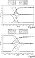
- the above discussed time interval occurs, during switching, in which biasing signals CP3_BOT, CP4_BOT are overlapping, in this case, at the low level (this time interval is also shown with the arrow in Figure 4A ).
- the gate terminal of the second decoupling transistor 15b is already low (causing turn-off of the same second decoupling transistor 15b), while the gate terminal of the first decoupling transistor 15a is switching in the same low state (thereby causing turn-off also of the first decoupling transistor 15a); accordingly, also the bottom level-shifted line LS_BOT is decoupled or isolated from the line at the level-shifted ground reference SHIFTED_GND (i.e. it is connected to the same level-shifted ground reference SHIFTED_GND via a very high resistance) during switching of the medium level shifted input voltage MLS_IN.
- a drop of the local supply voltage to the latching core 10 therefore occurs (i.e. a drop of the voltage at the top and bottom level-shifted lines LS_TOP, LS_BOT), which facilitates latch switching.
- the first and second latching units 10a, 10b are isolated from the supply during switching (i.e. they are left floating), providing for a very low energy consumption and a very fast switching of both the high-level shifted output voltage HLS_OUT and the medium-level shifted output voltage MLS_OUT, e.g. in the order of 200-250 ps.
- switching of the medium level shifted input voltage MLS_IN from the high to the low value (1 -> 0 switching transition) entails a wholly corresponding operation of the high-level shifting stage 4, again with the latching core 10 being isolated from the supply during commutation, thanks to the biasing signals CP1_BOT, CP2_BOT again overlapping at the high level and the biasing signals CP3_BOT, CP4_BOT again overlapping at the low level.
- the first high-level shifted input reset signal LS_RESET_P and the second high-level shifted input reset signal LS_RESET_N respectively active at a low level and at a high level, allow to reset, at any time, the state of the first and second latching units 10a, 10b of the latching core 10, in particular by setting the respective latching output L_OUT to the level-shifted ground reference SHIFTED_GND and, respectively, to the high supply voltage V PH .
- the level shifted input reset signal LS_RESET at the input of the AND logic gate 18, also sets a reset value for the biasing signals CP1_BOT, CP2_BOT and CP3_BOT, CP4_BOT, independently from the value of the medium level shifted input voltage MLS_IN.
- the reset generation stage 6 assures that the first high-level shifted input reset signal LS_RESET_P and the second high-level shifted input reset signal LS_RESET_N are available at any moment during operation of the level shifter circuit 1, and moreover that they are suitably generated with a voltage level that is always referred to proper shifted values, i.e. to the value of the intermediate and high supply voltages V PL , V PH (that may even change during operation, e.g. due to charge pump circuit stages generating the same voltages, as will be clear for a person skilled in the art).
- the first high-level shifted input reset signal LS_RESET_P and the second high-level shifted input reset signal LS_RESET_N are to be generated with values switching between the intermediate and the high supply voltages V PL , V PH .
- the reset generation stage 6 comprises a first generation circuit 6a, for generation of the first high-level shifted input reset signal LS_RESET_P, and a second generation circuit 6b, for generation of the second high-level shifted input reset signal LS_RESET_N.
- Each of the first and second generation circuits 6a, 6b includes: a respective storing capacitor 30; a refreshing unit 32; a first and a second boosting capacitors 33, 34; a boosting unit 35; and an output buffer 36.
- the refreshing unit 32 has a supply input coupled to the line at the high supply voltage V PH , in case of the first generation circuit 6a, and the intermediate supply voltage V PL in case of the second generation circuit 6b, and comprises refresh transistors of the PMOS type in case of the first generation circuit 6a and of the NMOS type in case of the second generation circuit 6b, and in particular: a first and a second refresh transistors 38a, 38b, coupled between the supply input and a top plate of the storing capacitor 30 (having a voltage denoted as LS_RESET_TOP_P for the first generation circuit 6a and as LS_RESET_TOP_N for the second generation circuit 6b), and having a gate terminal coupled to a top plate of the first, respectively, the second boosting capacitor 33, 34 (having voltages denoted as NLS_BOOSTED_P, LS_BOOSTED_P for the first generation circuit 6a and as NLS_BOOSTED_N, LS_BOOSTED_N for the second generation
- the boosting unit 35 includes logic gates (NAND logic gates in case of the first generation circuit 6a and NOR logic gates in case of the second generation circuit 6b), and in particular a first logic gate 39a and a second logic gate 39b.
- the first logic gate 39a has a first input receiving a timing or clock signal CK, a second input receiving the level shifted input reset signal LS_RESET, in case of the first generation circuit 6a, or a negated version of the same level shifted input reset signal LS_RESET, generated by a suitable inverter 40, in case of the second generation circuit 6b, a third input coupled to an output of the second logic gate 39b, and a respective output coupled to the bottom plate of the first boosting capacitor 33; and a second logic gate 39b, having a first input coupled to the output of the first logic gate 39a, a second input receiving the level shifted input reset signal LS_RESET, in case of the first generation circuit 6a, or a negated version of the same level shifted input reset signal LS_RESET, generated by the inverter 40, in case of the second generation circuit 6b, a third input, negated, receiving the clock signal CK (thus inputting a negated version thereof), and an output coupled to the bottom plate of the second
- the bottom plate of the storing capacitor 30 (having a voltage denoted as LS_RESET_BOT_P for the first generation circuit 6a and as LS_RESET_BOT_N for the second generation circuit 6b) is coupled to the output of a buffer 41, which receives at its input the level shifted input reset signal LS_RESET in case of the first generation circuit 6a; or it is coupled to the output of the inverter 40, in case of the second generation circuit 6b, thus receiving the negated version of the same level shifted input reset signal LS_RESET.
- the output buffer 36 is referred between the high power supply V PH and the intermediate power supply V PL and has an input coupled to the top plate of the storing capacitor 30 and an output defining the first reset output of the reset generation stage 6 providing the first high-level shifted input reset signal LS_RESET_P, in case of the first generation circuit 6a, or the second reset output of the same reset generation stage 6 providing the second high-level shifted input reset signal LS_RESET_N, in case of the second generation circuit 6b.
- the combined operation of the boosting unit 35, first and second boosting capacitors 33, 34 and refreshing unit 32 is that of continuously refreshing the voltage value stored in the storing capacitor 30; in particular, the bottom plate of the storing capacitor 30 is at the level of the intermediate supply voltage V PL , while the top plate of the same storing capacitor 30 is at the level of the high supply voltage V PH .
- the value of the first high-level shifted input reset signal LS_RESET_P at the output of the output buffer 36 is high, i.e. equal to the high supply voltage V PH ; as previously discussed, this value drives in the OFF state the first reset transistor 20a of the high-level shifting stage 4, since no reset is in this case required.
- either the output of the first logic gate 39a, or the output of the second logic gate 39b is high (while the output of the other logic gate is low), so that either the first or second boosting capacitor 33, 34 provides a boosted voltage at the gate terminals of the first and fourth refresh transistors 38a, 38d, respectively of the second and third refresh transistors 38b, 38c.
- the clock signal CK is at the high level ('1')
- the output of the first logic gate 39a is high and the output of the second logic gate 39b is low
- the clock signal CK is at the low level ('0')
- the output of the first logic gate 39a is low and the output of the second logic gate 39b is high.
- the top plate of the storing capacitor 30 is refreshed to the level of the high supply voltage V PH , either by the first and fourth refresh transistors 38a, 38d, or by the second and third refresh transistors 38b, 38c, being in the ON state.
- the level shifted input reset signal LS_RESET switches to the low level (in the discussed embodiment, being equal to the ground reference GND), so that the output of both the first and the second logic gates 39a, 39b is brought to the high level.
- the gate terminals of all refresh transistors 38a, 38b, 38c, 38d is high, and the same refresh transistors are all set in the OFF state, thus stopping refresh of the storing capacitor 30 to the high supply voltage V PH .
- the top plate of the same storing capacitor 30 undergoes a same voltage drop as the bottom plate, shifting from V PH to V PH -V PL , i.e. to the value of the intermediate supply voltage V PL , since in the discussed embodiment it is assumed that V PH ⁇ 2 ⁇ V PL .
- the value of the first high-level shifted input reset signal LS_RESET_P at the output of the output buffer 36 shifts to the low state, i.e. being equal to the intermediate supply voltage V PL ; as previously discussed, this value drives in the ON state the first reset transistor 20a of the high-level shifting stage 4, implementing reset of the second latching unit 10b.
- this reset condition may be maintained as long as the storing capacitor 30 maintains its charge, for example for a time interval in the order of 1 ⁇ s (as in the example shown in Figures 7A-7D ).
- Operation of the second generation circuit 6b corresponds to that of the first generation circuit 6a, so that it is not discussed in details.
- the bottom plate of the respective storing capacitor 30 is set at the ground reference GND, while the top plate of the same storing capacitor 30 is continuously refreshed at the value of the intermediate supply voltage V PL , that is provided at the supply input of the second generation circuit 6b, through the combined operation of the boosting unit 35, first and second boosting capacitors 33, 34 and refreshing unit 32.
- the value of the second high-level shifted input reset signal LS_RESET_N at the output of the respective output buffer 36 is low, i.e. equal to the intermediate supply voltage V PL ; as previously discussed, this value drives in the OFF state the second reset transistor 20b of the high-level shifting stage 4, since no reset is in this case required.
- the bottom plate of the storing capacitor 30 experiences an increase equal to the value of the intermediate supply voltage V PL , while refresh of the top plate thereof is stopped (since the output of both first and second logic gates 39a, 39b is brought to the low level, thus driving all refresh transistors 38a-38d in the OFF state).
- the top plate of the same storing capacitor 30 undergoes a same voltage increase as the bottom plate, shifting from V PL to V PL +V PL , i.e. to the value of the high supply voltage V PH , since in the discussed embodiment it is assumed that V PH ⁇ 2 ⁇ V PL .
- the value of the second high-level shifted input reset signal LS_RESET_N at the output of the output buffer 36 shifts to the high state, i.e. being equal to the high supply voltage V PH ; as previously discussed, this value drives in the ON state the second reset transistor 20b of the high-level shifting stage 4, implementing reset of the first latching unit 10a.
- the value of the first and second high-level shifted reset signals LS_RESET_P LS_RESET_N follows possible variations of the supply voltage (in the example, an increase of the high supply voltage V PH is shown), in a very short time.
- the level shifter circuit 1 may find advantageous application in an integrated non-volatile memory device.
- a non-volatile memory device designated by 100, comprises in general a memory array 42 constituted by a plurality of memory cells 43, arranged in wordlines WL and bitlines BL.
- Each memory cell 43 is constituted by a storage element, including a phase-change material element (for example, a chalcogenide, such as GST) in the example shown of PCM memories and an access transistor (in the case shown a BJT transistor), appropriately connected to a respective bitline BL and to a respective wordline WL.
- a phase-change material element for example, a chalcogenide, such as GST
- an access transistor in the case shown a BJT transistor
- a column decoder 44 and a row decoder 45 enable selection of the memory cells 43 on the basis of address signals received at the input (generated in a known way and designated as a whole by AS) and appropriate decoding schemes, and in particular selection of the corresponding bitlines BL and of the corresponding wordlines WL, each time addressed, enabling their biasing at desired voltage and current values during the reading and programming operations, by means of appropriate driving stages.
- a reading stage is selectively coupled to the memory array 42 via the column decoder 44, during the operations of reading of the contents of the memory cells 43.
- the level shifter circuit 1 may, for example, be used within the column and row decoders 44, 45 to enable generation of the appropriate quantities, for selection and biasing of the bitlines BL and wordlines WL.
- the column decoder 44 may have, in a per se known manner, a hierarchical decoding structure, with a number of decoding stages.
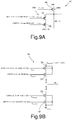
- a first decoding stage 44a includes a plurality of global-selection transistors 46 (only one of which is shown in the schematic depiction of Figure 9A ), in the example of a PMOS type, which enable selection and biasing of a respective global bitline (or main bitline) MBL, for a respective sector of the memory array 42 (here not shown).
- Each global-selection transistor 46 receives on a control terminal thereof a respective global-selection signal YN ⁇ k>, having a first value, for example a low value, for connecting the respective global bitline MBL to a respective module (driver) of the driving stage of the non-volatile memory device 100, which supplies a driving signal YMP, and a second value, in the example high, for disconnecting the same global bitline MBL from the driving stage.
- a second decoding stage 44b includes a plurality of local-selection transistors 48 (again, only one of which is shown in Figure 9A ), in the example of a PMOS type, for each sector of the memory array 42, each connected between a respective global bitline MBL and a respective local bit line BL to which memory cells 43 are connected (not illustrated herein).
- Each local-selection transistor 48 receives on a control terminal thereof a respective local-selection signal YO ⁇ i>, which has a first value, for example low, for connecting the global bitline MBL associated to the respective sector to a respective local bitline BL (and to the associated memory cells 43), and a second value, in the example high, for disconnecting the same global bitline MBL from the respective bitline BL.
- a cascode transistor 49 is coupled between the local bitline BL and each local-selection transistor 48, having a control terminal receiving a cascode voltage V CASC , with a value suitable to avoid over-voltages across the decoder transistor terminals (for example, transistors may be sized so that a maximum voltage allowed between their terminals is equal to 1.8 V).
- the global-selection signal YN ⁇ k> and the local-selection signal YO ⁇ i> are referred to shifted voltage values, e.g. equal to 4.2V or 2.1V depending on the memory operation being performed and may be generated by a respective level shifter circuit 1 (as the one previously disclosed in details). Also the cascode voltage V CASC is required to have suitable shifted voltages, e.g. equal to 2.1 V and may be also generated by level shifter circuit 1.
- the two parallel shifting paths present in the level shifter circuit 1 may be exploited to generate the intermediate supply voltage V PL , in this case corresponding to the cascode voltage V CASC ; and the high supply voltage V PH , in this case corresponding to the global-selection signal YN ⁇ k> and local-selection signal YO ⁇ i>.
- level shifter circuits 1 is also required in the row decoders 45.
- the row decoder 45 may envisage that word lines WL are normally biased to a positive voltage in an unselected status, and grounded when selected.
- the row decoder 44 may include a pull-up transistor 50, of a PMOS type, controllable to couple the word line WL to a row decoder supply voltage V ROWDEC (e.g. equal to 4.2V for writing operations or 1,5V for reading operations); a first cascode transistor 51, also of a PMOS type, may again be coupled between the word line WL and the respective pull-up transistor 50, for overvoltage protection, receiving a first cascode voltage V CASCP at the control terminal.
- V ROWDEC row decoder supply voltage
- the control terminal of the a pull-up transistor 50 may require e.g. voltages V PUP equal to 4.2V or 2.1V during writing and 1.5V or 0V during reading operations; while the first cascode voltage V CASCP provided to the control terminal of the first cascode transistor 51 may be equal to 2,1V or 0V during writing or, respectively, reading operations.
- the row decoder 45 may include a pull-down transistor 52, of a NMOS type, controllable to couple the word line WL to a ground reference GND; a second cascode transistor 53, also of a NMOS type, may again be coupled between the word line WL and the respective pull-down transistor 52, for overvoltage protection, receiving a second cascode voltage V CASCN at the control terminal.
- the control terminal of the pull-down transistor 52 may require e.g. voltages V PDOWN equal to 2.1V or 0V during writing and 1.5V or 0V during reading operations; while the second cascode voltage V CASCN provided to the control terminal of the second cascode transistor 53 may be equal to 2.1V or 1.8V during writing or, respectively, reading operations.
- the two parallel shifting paths present in the level shifter circuit 1 may in this case be exploited to generate the first and second cascode voltages V CASCP , V CASCN , required for the above discussed different voltage domains.
- simultaneous switching transitions obtained for the first and second cascode voltages V CASCP , V CASCN allow to avoid crossbar currents between supply and ground reference in the row decoder 45.
- level shifting operations in the medium-voltage and high-voltage domains are performed in parallel, with minimum delays between the level transitions, so as to avoid current cross-conductions, e.g. through NMOS and PMOS transistors.
- the level shifter circuit 1 also provides a dedicated reset scheme for initialization, with properly level-shifted reset signals, which are also able to adapt to the supply voltage values that are applied.
- the proposed solution is therefore particularly advantageous in particularly scaled technologies (for example, the 28-nm FD-SOI technology), and, in general, for applications in non-volatile memory devices, for example in corresponding column and/or row decoders.
Landscapes
- Engineering & Computer Science (AREA)
- Computer Hardware Design (AREA)
- Physics & Mathematics (AREA)
- Computing Systems (AREA)
- General Engineering & Computer Science (AREA)
- Mathematical Physics (AREA)
- Microelectronics & Electronic Packaging (AREA)
- Chemical & Material Sciences (AREA)
- Crystallography & Structural Chemistry (AREA)
- Power Engineering (AREA)
- Logic Circuits (AREA)
- Techniques For Improving Reliability Of Storages (AREA)
Abstract
Description
- The present solution relates to a level shifter circuit having improved efficiency, in particular for use in a memory device, and to a corresponding memory device, in particular of a non-volatile type.
- As it is known, level shifter circuits (in short, level shifters) have several applications, wherever it is required to interface two or more circuits operating at different voltage levels.
- Level shifters are used in non-volatile memory devices, for example of a PCM (Phase-Change Memory) type, where storage of information is obtained by exploiting phase-change materials (e.g. "chalcogenides" or "chalcogenic materials"), having the property of switching between phases that have resistivity of considerably different value.
- In these memory devices, an internal supply voltage is present (the so-called logic supply voltage Vdd, with low voltage values, for example comprised between 1 V and 1.35 V). In order to perform reading and writing (programming or erasing) operations on the contents of the memory cells, use of higher operating voltages, for example up to values of 4.5 V, is required.
- Due to the different ranges of values of the voltages present in these memory devices, use of level shifter circuits is required, in order to interface and operatively couple low-voltage and high-voltage circuit portions.
- In particular, it is often required to have two distinct level-shifted voltage domains, i.e. a medium-voltage domain (with voltages in the range between a ground reference and a medium, or intermediate, voltage level, e.g. 2.25 V) and a high-voltage domain (with voltages in the range between the medium voltage level and a high voltage level, e.g. 4.5 V).
- For example, in non-volatile memory application, particularly in PCM memories, row and column decoders require voltages shifted in the medium-voltage and high-voltage domains for their operation (as will also be discussed in the following).
-
US 2002/180508 A1 ,US 2002/080651 A1 andUS 2018/061495 disclose known level-shifter circuits for use in semiconductor memory devices. - Common desired requirements for the level shifters, particularly for memory applications, are fast level transitions, low power consumption and small area occupation.
- It is also a desired requirement that level shifting operations in the medium-voltage and high-voltage domains are performed in parallel, with minimum delays between the level transitions, for example in order to avoid current cross-conductions in corresponding NMOS and PMOS transistors. Another common desired requirement is for the level shifter to offer flexibility as regards the supply voltage values that may be applied.
- The present Applicant has realized that known level shifters solutions are not satisfactory in meeting the above requirements.
- The aim of the present solution is to solve the problems highlighted previously, and in particular to provide an improved solution for a level shifter circuit.
- According to the present invention, a level shifter circuit, and a corresponding memory device are consequently provided as defined in the annexed claims.
- For a better understanding of the present invention, preferred embodiments thereof are now described, purely by way of non-limiting example and with reference to the attached drawings, wherein:
-
Figure 1 shows a schematic block diagram of a level shifter circuit according to an embodiment of the present solution; -
Figure 2 shows a possible circuit configuration of an input stage for medium voltage level shifting operations in the level shifter circuit ofFigure 1 ; -
Figure 3 shows a detailed circuit diagram of a high-voltage level shifter stage in the level shifter circuit ofFigure 1 ; -
Figures 4A-4B and5A-5B show plots of electrical quantities related to operation of the high-voltage level shifter stage; -
Figure 6 shows a detailed circuit diagram of a reset buffer stage in the level shifter circuit ofFigure 1 ; -
Figures 7A-7D show plots of electrical quantities related to operation of the reset buffer stage; -
Figure 8 shows a block diagram of a memory device using the level shifter circuit ofFigure 1 , in corresponding address-decoder stages; -
Figure 9A is a schematic depiction of a portion of a column decoder in the memory device ofFigure 8 ; and -
Figure 9B is a schematic depiction of a portion of a row decoder in the memory device ofFigure 8 . - With initial reference to
Figure 1 , an embodiment of a level shifter circuit, designated as a whole by 1, is now described. - The level shifter circuit 1 comprises an
input stage 2, which receives an input signal LV_IN at a low voltage level, i.e. in a range [GND, Vdd], where Vdd is a logic supply voltage with a value that is for example comprised between 1 V and 1.35 V; and provides at the output a medium level shifted input voltage MLS_IN, in the medium-voltage domain, with voltages in the range [GND, VPL], between the ground reference GND and an intermediate supply voltage VPL at medium voltage, with a value greater than the logic supply voltage Vdd, for example comprised between 1.2 V and 2.25 V (in the exemplary application for a non-volatile memory, the value of the intermediate supply voltage VPL may depend on the memory operation being performed, being it a reading or a writing operation). - The
input stage 2 implements a medium voltage shifting of the input signal LV_IN, and may have any known circuit configuration suitable for medium voltage shifting. For example,Figure 2 shows a possible circuit configuration (here not disclosed in detail) for theinput stage 2, implementing medium-voltage level shifting of the input signal LV_IN to generate the corresponding medium-level shifted input voltage MLS_IN. - The level shifter circuit 1 further comprises (see again
Figure 1 ) a high-level shifting stage 4, having a signal input receiving the medium-level shifted input voltage MLS_IN, and a first output providing a corresponding high-level shifted output voltage HLS_OUT, in the range [VPL, VPH], between the intermediate supply voltage VPL and a high supply voltage VPH, at a high voltage level with a value greater than the intermediate supply voltage VPL, for example comprised between 1.2 V and 4.5 V (in the exemplary application for a non-volatile memory, also the value of the high supply voltage VPH may depend on the memory operation being performed, being it a reading or a writing operation). The high-level shifting stage 4 thus has: a first supply input, receiving the intermediate supply voltage VPL and a second supply input receiving the high supply voltage VPH; and moreover a shifted-ground input, receiving a level-shifted ground reference SHIFTED_GND, having a voltage value higher than the ground reference GND, in the present embodiment equal to 2.25 V. - According to an aspect of the present solution, the high-
level shifting stage 4 also has a second output providing a corresponding medium-level shifted output voltage MLS_OUT, in the range [GND, VPL], which has corresponding and substantially simultaneous transitions as the high-level shifted output voltage HLS_OUT. - Moreover, the high-
level shifting stage 4 has: a first reset input, receiving a level shifted input reset signal LS_RESET, in the medium-voltage domain [GND, VPL]; a second reset input, receiving a first high-level shifted input reset signal LS_RESET_P, in the high-voltage domain [VPL, VPH]; and a third reset input, receiving a second high-level shifted input reset signal LS_RESET_N, also in the high-voltage domain [VPL, VPH], with opposite level transitions with respect to the first high-level shifted input reset signal LS_RESET_P. - The level shifter circuit 1 further comprises a
reset generation stage 6, having an input receiving the level shifted input reset signal LS_RESET, and configured to perform high-level shifting operations to generate at a first reset output the first high-level shifted input reset signal LS_RESET_P, and at a second reset output the second high-level shifted input reset signal LS_RESET_N, both having transitions corresponding to the level shifted input reset signal LS_RESET; thereset generation stage 6 also has respective first and a second supply inputs receiving the intermediate supply voltage VPL and, respectively, the high supply voltage VPH, and moreover a clock input, receiving a level-shifted clock signal LS_CK, as a timing signal, also being in the medium-voltage domain [GND, VPL]. - In particular, the level shifted input reset signal LS_RESET is generated by a first medium-
voltage shifting stage 8a, which receives at an input a low-voltage input reset signal LV_RESET; and the level-shifted clock signal LS_CK is generated by a second medium-voltage shifting stage 8b, which receives at a respective input a low-voltage input clock signal LV_CK (both first and second medium-voltage shifting stages Figure 2 ). - In the embodiment shown in
Figure 1 , the level shifter circuit 1 moreover comprises: afirst inverting stage 9a, supplied by the high supply voltage VPH, that receives the high-level shifted output voltage HLS_OUT from the high-level shifting stage 4 and provides, at a first output terminal of the same level shifter circuit 1, a first output voltage HV_OUT, with transitions in the high-voltage domain [VPL, VPH] (in the example, switching between 2.25 V and 4.5 V); and asecond inverting stage 9b, supplied by the intermediate supply voltage VPL, that receives the medium-level shifted output voltage MLS_OUT from the same high-level shifting stage 4 and provides, at a second output terminal of the same level shifter circuit 1, a second output voltage MV_OUT, with corresponding and simultaneous transitions in the medium-voltage domain [GND, VPL] (in the example, switching between 0 V and 2.25 V). - As schematically shown, the first output voltage HV_OUT can be provided, for example, to the base terminal of a PMOS transistor, having a conduction terminal coupled to the high supply voltage VPH, to switch the same PMOS transistor in a ON or OFF state; in a corresponding manner, the second output voltage MV_OUT can be provided, for example, to the base terminal of a NMOS transistor, having a conduction terminal coupled to the ground reference GND, to switch the same NMOS transistor in a ON or OFF state.
- With reference to
Figure 3 , an embodiment of the highlevel shifting stage 4 is now discussed in greater details. - The high
level shifting stage 4 includes a latching (or holding)core 10, which is configured to switch its latching state in response to the transitions of the medium level shifted input voltage MLS_IN and to maintain the latching state until a next transition of the same medium level shifted input voltage MLS_IN, or a reset input, is received. - The latching
core 10 includes a first and asecond latching units second latch inverters - Each of the first and
second inverters first latching unit 10a and as MN4-MP4 and MN5-MP5 for thesecond latching unit 10b), with first conduction terminals coupled to the bottom level-shifted line LS_BOT and the top level-shifted line LS_TOP, second conduction terminals coupled together and to the latching output L_OUT or latching input L_IN, and gate terminals coupled together and to the latching output L_OUT or latching input L_IN. - The high
level shifting stage 4 further includes a capacitive-coupling unit 13 for eachlatching unit first coupling capacitor 13a, having a top plate coupled to the latching input L_IN of therespective latching unit second coupling capacitor 13b, having a top plate coupled to the latching output L_OUT of therespective latching unit - The high
level shifting stage 4 moreover comprises a first and asecond decoupling units first decoupling unit 14 operable to selectively couple/decouple the top level-shifted line LS_TOP to/from a line set at the high supply voltage VPH, and thesecond decoupling unit 15 operable to selectively couple/decouple the bottom level-shifted line LS_BOT to/from a line set at the level-shifted ground reference SHIFTED_GND. - In particular, the
first decoupling unit 14 includes a first and a secondPMOS decoupling transistors first coupling capacitor 13a and, respectively, to the top plate of thesecond coupling capacitor 13b of the capacitive-coupling unit 13 coupled to thefirst latching unit 10a, receiving respective biasing signals CP1_TOP, CP2_TOP. - In a corresponding manner, the
second decoupling unit 15 includes a first and a secondNMOS decoupling transistors first coupling capacitor 13a and, respectively, to the top plate of thesecond coupling capacitor 13b of the capacitive-coupling unit 13 coupled to thesecond latching unit 10b, receiving respective biasing signals CP3_TOP, CP4_TOP. - The high
level shifting stage 4 further comprises adriving stage 16 including a first and asecond driving units first driving unit 16a being configured to bias the bottom plates of the first andsecond coupling capacitors first latching unit 10a with respective biasing signals CP1_BOT, CP2_BOT; and thesecond driving unit 16b being configured to drive the bottom plates of the first andsecond coupling capacitors second latching unit 10b with respective biasing signals CP3_BOT, CP4_BOT. - The first and
second coupling capacitors second latching units respective latching unit driving stage 16 carrying the biasing signals CP1_BOT-CP4_BOT (in particular to the output lines of the first and, respectively,second driving units - According to a particular aspect of the present solution, the first and
second driving units - In particular, the
first driving unit 16a is of the NAND logic type and is configured to generate the respective biasing signals CP1_BOT, CP2_BOT with positive overlapping values during switching of the medium level shifted input voltage MLS_IN, so as to drive (as will also be detailed in the following) the gate terminals of the first and secondPMOS decoupling transistors first decoupling unit 14 both at a high value (corresponding to the high supply voltage VPH), thus turning off the samePMOS decoupling transistors - In a corresponding manner, the
second driving unit 16b is of the NOR logic type and is configured to generate the respective biasing signals CP3_BOT, CP4_BOT with negative overlapping values during switching of the medium level shifted input voltage MLS_IN, so as to drive (as will also be detailed in the following) the gate terminals of the first and secondNMOS decoupling transistors second decoupling unit 15 both at a low value (corresponding to the level-shifted ground reference SHIFTED_GND), thus turning off the sameNMOS decoupling transistors - Both the first and the
second driving units AND logic gate 18, receiving at its inputs the medium level shifted input voltage MLS_IN and the level shifted input reset signal LS_RESET. - In more details, the
first driving unit 16a includes a first and a secondNAND logic gates 16a', 16a", wherein: the firstNAND logic gate 16a' has a first input coupled to the output of theAND logic gate 18 receiving the biasing input P_IN, a second input coupled to the output of the secondNAND logic gate 16a", and an output coupled to the bottom plate of thefirst coupling capacitor 13a of thefirst latching unit 10a; and the secondNAND logic gate 16a" has a first, negated, input coupled to the output of theAND logic gate 18 and receiving the negated biasing input, a second input coupled to the output of the firstNAND logic gate 16a', and an output coupled to the bottom plate of thesecond coupling capacitor 13b of thefirst latching unit 10a. - The
second driving unit 16b includes a first and a secondNOR logic gates 16b', 16b", wherein: the firstNOR logic gate 16b' has a first input coupled to the output of theAND logic gate 18 and receiving the biasing input P_IN, a second input coupled to the output of the secondNOR logic gate 16b", and an output coupled to the bottom plate of thefirst coupling capacitor 13a of thesecond latching unit 10b; and the secondNOR logic gate 16b" has a first, negated, input coupled to the output of theAND logic gate 18 and receiving the negated biasing input, a second input coupled to the output of the firstNOR logic gate 16b', and an output coupled to the bottom plate of thesecond coupling capacitor 13b of thesecond latching unit 10b. - The high-
level shifting stage 4 further comprises anoutput inverter unit 19, having an input coupled to the latching output L_OUT of thesecond latching unit 10b (and to the top plate of thesecond coupling capacitor 13b of thesecond latching unit 10b), and an output defining the first output of the high-level shifting stage 4 providing the high-level shifted output voltage HLS_OUT. - In more details, the
output inverter unit 19 includes aPMOS transistor 19a, having a first conduction terminal coupled to the line at the high supply voltage VPH, a second conduction terminal coupled to the first output of the high-level shifting stage 4, and a gate terminal coupled to the top plate of thesecond coupling capacitor 13b of thesecond latching unit 10b and receiving the control signals CP3_TOP; and aNMOS transistor 19b, having a first conduction terminal coupled to the line at the level-shifted ground reference SHIFTED_GND, a second conduction terminal coupled to the first output of the high-level shifting stage 4, and a gate terminal coupled to the top plate of thesecond coupling capacitor 13b of thesecond latching unit 10b and receiving the same control signals CP3_TOP. - Moreover, the high-
level shifting stage 4 comprises: afirst reset transistor 20a, of the PMOS type, having a first conduction terminal coupled to the line at the high supply voltage VPH, a second conduction terminal coupled to the latching output L_OUT of thesecond latching unit 10b (and to the top plate of thesecond coupling capacitor 13b of the samesecond latching unit 10b), and a gate terminal coupled to the second reset input of the high-level shifting stage 4, receiving the first high-level shifted input reset signal LS_RESET_P; and asecond reset transistor 20b, of the NMOS type, having a first conduction terminal coupled to the line at the level-shifted ground reference SHIFTED_GND, a second conduction terminal coupled to the latching output L_OUT of thefirst latching unit 10a (and to the top plate of thesecond coupling capacitor 13b of the samefirst latching unit 10a), and a gate terminal coupled to the third reset input of the same high-level shifting stage 4, receiving the second high-level shifted input reset signal LS_RESET_N. - The high-
level shifting stage 4 further comprises anoutput inverting buffer 22, having an input coupled to the output of the firstNOR logic gate 16b' of thesecond driving unit 16b (and the bottom plate of thesecond coupling capacitor 13b of thesecond latching unit 10b), receiving the biasing signal CP3_BOT, and an output defining the second output of the high-level shifting stage 4 providing the medium-level shifted output voltage MLS_OUT. - Operation of the high-
level shifting stage 4 is now discussed, also referring to the plots of the relevant signals shown inFigure 4A, 4B andFigure 5A, 5B . - In general, operation of the high-
level shifting stage 4 is based on inputting the switching transitions of the medium level shifted input voltage MLS_IN into the latchingcore 10 via capacitive coupling, through the capacitive-coupling units 13, determining shifting of the biasing signals and switching of the latching state. - According to a particular aspect of the present solution, local supply to the first and
second latching units transistors second decoupling units latching units same latching units - According to the above, advantageously, reduced capacitance values and minimum-sized transistors may be used in the level shifter circuit 1, with a great saving in term of area occupation.
- In more details, let's suppose that the medium level shifted input voltage MLS_IN switches from the low (GND) to a high value (i.e. equal to the intermediate supply voltage VPL) for a 0 -> 1 switching transition, with the level shifted input reset signal LS_RESET being inactive (in this case, as will be discussed in detail also in the following, being at the high level, i.e. equal to the intermediate supply voltage VPL).
- Before switching, the output of the first
NAND logic gate 16a' of thefirst driving unit 16a is in the high state ('1'), while the output of the secondNAND logic gate 16a" of the samefirst driving unit 16a is in the low state ('0'). - At the rising edge of the medium level shifted input voltage MLS_IN, the output of the second
NAND logic gate 16a" immediately switches to the high state, while the output of the firstNAND logic gate 16a' is still in the high state; indeed, switching of the output of the firstNAND logic gate 16a' to the low state may occur only after a certain delay, due to propagation delay of the signals from the secondNAND logic gate 16a". - Therefore, there is a time interval, during switching, e.g. in the order of 100-150 ps (10-12 s), in which biasing signals CP1_BOT, CP2_BOT are overlapping at the high level (this time interval is shown with the arrow in
Figure 4A , relating to the 0 -> 1 switching transition). In particular, the gate terminal of thefirst decoupling transistor 14a is already high (causing turn-off of thefirst decoupling transistor 14a), while the gate terminal of thesecond decoupling transistor 14b is switching in the same high state (thereby causing turn-off also of thesecond decoupling transistor 14b); accordingly, the top level-shifted line LS_TOP is decoupled or isolated from the line at the high supply voltage VPH (i.e. it is connected to the same high supply voltage VPH via a very high resistance) during switching of the medium level shifted input voltage MLS_IN. - Operation of the
second driving unit 16b substantially corresponds to what discussed above for thefirst driving unit 16a. - In this case, before switching, the output of the second NOR
logic gate 16b" of thesecond driving unit 16b is initially in the low state ('0'), while the output of the first NORlogic gate 16b' is in the high state ('1'). - At the rising edge of the medium level shifted input voltage MLS_IN, the output of the first NOR
logic gate 16b' immediately switches to the low state, while the output of the second NORlogic gate 16b" is still in the low state; indeed, switching of the output of the second NORlogic gate 16b" to the high state may occur only after a certain delay, due to the propagation of the signals from the first NORlogic gate 16b'. - Therefore, the above discussed time interval occurs, during switching, in which biasing signals CP3_BOT, CP4_BOT are overlapping, in this case, at the low level (this time interval is also shown with the arrow in
Figure 4A ). In particular, the gate terminal of thesecond decoupling transistor 15b is already low (causing turn-off of the samesecond decoupling transistor 15b), while the gate terminal of thefirst decoupling transistor 15a is switching in the same low state (thereby causing turn-off also of thefirst decoupling transistor 15a); accordingly, also the bottom level-shifted line LS_BOT is decoupled or isolated from the line at the level-shifted ground reference SHIFTED_GND (i.e. it is connected to the same level-shifted ground reference SHIFTED_GND via a very high resistance) during switching of the medium level shifted input voltage MLS_IN. - As shown in
Figure 4A , a drop of the local supply voltage to the latchingcore 10 therefore occurs (i.e. a drop of the voltage at the top and bottom level-shifted lines LS_TOP, LS_BOT), which facilitates latch switching. The first andsecond latching units - In particular, as shown in
Figure 5A (again relating to the 0 -> 1 switching transition), the transitions of the high-level shifted output voltage HLS_OUT and the medium-level shifted output voltage MLS_OUT occur substantially at a same time, with no appreciable delay therebetween. As will be readily appreciated by those skilled in the art, this feature is of great relevance, e.g. to avoid so called cross-conduction or "crossbar" currents between PMOS and NMOS transistors. - As it will be clear based on the previous discussion, and as shown in
Figures 5A and 5B , switching of the medium level shifted input voltage MLS_IN from the high to the low value (1 -> 0 switching transition) entails a wholly corresponding operation of the high-level shifting stage 4, again with the latchingcore 10 being isolated from the supply during commutation, thanks to the biasing signals CP1_BOT, CP2_BOT again overlapping at the high level and the biasing signals CP3_BOT, CP4_BOT again overlapping at the low level. - According to a further aspect of the present solution, the first high-level shifted input reset signal LS_RESET_P and the second high-level shifted input reset signal LS_RESET_N, respectively active at a low level and at a high level, allow to reset, at any time, the state of the first and
second latching units core 10, in particular by setting the respective latching output L_OUT to the level-shifted ground reference SHIFTED_GND and, respectively, to the high supply voltage VPH. - Moreover, the level shifted input reset signal LS_RESET, at the input of the AND
logic gate 18, also sets a reset value for the biasing signals CP1_BOT, CP2_BOT and CP3_BOT, CP4_BOT, independently from the value of the medium level shifted input voltage MLS_IN. - A possible circuit embodiment and the operation of the
reset generation stage 6 of the level shifter circuit 1 are now discussed, according to a further aspect of the present solution. - The
reset generation stage 6 assures that the first high-level shifted input reset signal LS_RESET_P and the second high-level shifted input reset signal LS_RESET_N are available at any moment during operation of the level shifter circuit 1, and moreover that they are suitably generated with a voltage level that is always referred to proper shifted values, i.e. to the value of the intermediate and high supply voltages VPL, VPH (that may even change during operation, e.g. due to charge pump circuit stages generating the same voltages, as will be clear for a person skilled in the art). - As previously discussed, the first high-level shifted input reset signal LS_RESET_P and the second high-level shifted input reset signal LS_RESET_N are to be generated with values switching between the intermediate and the high supply voltages VPL, VPH.
- As shown in
Figure 6 , thereset generation stage 6 comprises afirst generation circuit 6a, for generation of the first high-level shifted input reset signal LS_RESET_P, and asecond generation circuit 6b, for generation of the second high-level shifted input reset signal LS_RESET_N. - Each of the first and
second generation circuits respective storing capacitor 30; arefreshing unit 32; a first and a second boostingcapacitors unit 35; and anoutput buffer 36. - In detail, the
refreshing unit 32 has a supply input coupled to the line at the high supply voltage VPH, in case of thefirst generation circuit 6a, and the intermediate supply voltage VPL in case of thesecond generation circuit 6b, and comprises refresh transistors of the PMOS type in case of thefirst generation circuit 6a and of the NMOS type in case of thesecond generation circuit 6b, and in particular: a first and asecond refresh transistors first generation circuit 6a and as LS_RESET_TOP_N for thesecond generation circuit 6b), and having a gate terminal coupled to a top plate of the first, respectively, the second boostingcapacitor 33, 34 (having voltages denoted as NLS_BOOSTED_P, LS_BOOSTED_P for thefirst generation circuit 6a and as NLS_BOOSTED_N, LS_BOOSTED_N for thesecond generation circuit 6b); and a third and afourth refresh transistors capacitor capacitor - The boosting
unit 35 includes logic gates (NAND logic gates in case of thefirst generation circuit 6a and NOR logic gates in case of thesecond generation circuit 6b), and in particular afirst logic gate 39a and asecond logic gate 39b. - The
first logic gate 39a has a first input receiving a timing or clock signal CK, a second input receiving the level shifted input reset signal LS_RESET, in case of thefirst generation circuit 6a, or a negated version of the same level shifted input reset signal LS_RESET, generated by asuitable inverter 40, in case of thesecond generation circuit 6b, a third input coupled to an output of thesecond logic gate 39b, and a respective output coupled to the bottom plate of the first boostingcapacitor 33; and asecond logic gate 39b, having a first input coupled to the output of thefirst logic gate 39a, a second input receiving the level shifted input reset signal LS_RESET, in case of thefirst generation circuit 6a, or a negated version of the same level shifted input reset signal LS_RESET, generated by theinverter 40, in case of thesecond generation circuit 6b, a third input, negated, receiving the clock signal CK (thus inputting a negated version thereof), and an output coupled to the bottom plate of the second boostingcapacitor 34. - The bottom plate of the storing capacitor 30 (having a voltage denoted as LS_RESET_BOT_P for the
first generation circuit 6a and as LS_RESET_BOT_N for thesecond generation circuit 6b) is coupled to the output of abuffer 41, which receives at its input the level shifted input reset signal LS_RESET in case of thefirst generation circuit 6a; or it is coupled to the output of theinverter 40, in case of thesecond generation circuit 6b, thus receiving the negated version of the same level shifted input reset signal LS_RESET. - The
output buffer 36 is referred between the high power supply VPH and the intermediate power supply VPL and has an input coupled to the top plate of the storingcapacitor 30 and an output defining the first reset output of thereset generation stage 6 providing the first high-level shifted input reset signal LS_RESET_P, in case of thefirst generation circuit 6a, or the second reset output of the samereset generation stage 6 providing the second high-level shifted input reset signal LS_RESET_N, in case of thesecond generation circuit 6b. - Operation of the
reset generation stage 6 is now discussed in more details, also referring to the diagrams of the relevant electrical quantities shown inFigures 7A-7D ; in particular, reference is made first to thefirst generation circuit 6a. - When the level shifted input reset signal LS_RESET is not active (in the discussed embodiment, being at the high level, i.e. equal to the intermediate supply voltage VPL), the combined operation of the boosting
unit 35, first and second boostingcapacitors refreshing unit 32 is that of continuously refreshing the voltage value stored in the storingcapacitor 30; in particular, the bottom plate of the storingcapacitor 30 is at the level of the intermediate supply voltage VPL, while the top plate of thesame storing capacitor 30 is at the level of the high supply voltage VPH. - Accordingly, the value of the first high-level shifted input reset signal LS_RESET_P at the output of the
output buffer 36 is high, i.e. equal to the high supply voltage VPH; as previously discussed, this value drives in the OFF state thefirst reset transistor 20a of the high-level shifting stage 4, since no reset is in this case required. - In more details, at each half period of the clock signal CK, either the output of the
first logic gate 39a, or the output of thesecond logic gate 39b is high (while the output of the other logic gate is low), so that either the first or second boostingcapacitor fourth refresh transistors third refresh transistors first logic gate 39a is high and the output of thesecond logic gate 39b is low; whereas, when the clock signal CK is at the low level ('0'), the output of thefirst logic gate 39a is low and the output of thesecond logic gate 39b is high. - Accordingly, at each half period of the clock signal CK, the top plate of the storing
capacitor 30 is refreshed to the level of the high supply voltage VPH, either by the first andfourth refresh transistors third refresh transistors - When the reset signal is to be activated, the level shifted input reset signal LS_RESET switches to the low level (in the discussed embodiment, being equal to the ground reference GND), so that the output of both the first and the
second logic gates refresh transistors capacitor 30 to the high supply voltage VPH. - Therefore, the top plate of the
same storing capacitor 30 undergoes a same voltage drop as the bottom plate, shifting from VPH to VPH-VPL, i.e. to the value of the intermediate supply voltage VPL, since in the discussed embodiment it is assumed that VPH≈2·VPL. - Accordingly, the value of the first high-level shifted input reset signal LS_RESET_P at the output of the
output buffer 36 shifts to the low state, i.e. being equal to the intermediate supply voltage VPL; as previously discussed, this value drives in the ON state thefirst reset transistor 20a of the high-level shifting stage 4, implementing reset of thesecond latching unit 10b. - It is noted that this reset condition may be maintained as long as the storing
capacitor 30 maintains its charge, for example for a time interval in the order of 1 µs (as in the example shown inFigures 7A-7D ). - Operation of the
second generation circuit 6b corresponds to that of thefirst generation circuit 6a, so that it is not discussed in details. - In this case, when reset is not active, the bottom plate of the
respective storing capacitor 30 is set at the ground reference GND, while the top plate of thesame storing capacitor 30 is continuously refreshed at the value of the intermediate supply voltage VPL, that is provided at the supply input of thesecond generation circuit 6b, through the combined operation of the boostingunit 35, first and second boostingcapacitors refreshing unit 32. - Accordingly, the value of the second high-level shifted input reset signal LS_RESET_N at the output of the
respective output buffer 36 is low, i.e. equal to the intermediate supply voltage VPL; as previously discussed, this value drives in the OFF state thesecond reset transistor 20b of the high-level shifting stage 4, since no reset is in this case required. - When the reset signal is to be activated and the level shifted input reset signal LS_RESET switches to the low level, the bottom plate of the storing
capacitor 30 experiences an increase equal to the value of the intermediate supply voltage VPL, while refresh of the top plate thereof is stopped (since the output of both first andsecond logic gates refresh transistors 38a-38d in the OFF state). - Therefore, the top plate of the
same storing capacitor 30 undergoes a same voltage increase as the bottom plate, shifting from VPL to VPL+VPL, i.e. to the value of the high supply voltage VPH, since in the discussed embodiment it is assumed that VPH≈2·VPL. - Accordingly, the value of the second high-level shifted input reset signal LS_RESET_N at the output of the
output buffer 36 shifts to the high state, i.e. being equal to the high supply voltage VPH; as previously discussed, this value drives in the ON state thesecond reset transistor 20b of the high-level shifting stage 4, implementing reset of thefirst latching unit 10a. - As shown in
Figures 7A-7C , the value of the first and second high-level shifted reset signals LS_RESET_P LS_RESET_N follows possible variations of the supply voltage (in the example, an increase of the high supply voltage VPH is shown), in a very short time. - Indeed, just a few clock cycles (e.g. less than five clock cycles) are sufficient for the refresh operations performed on the storing
capacitor 30 to bring the voltage of the top plate of thesame storing capacitor 30 to the new value of the supply voltage (in the example shown, experiencing a corresponding increase as the high supply voltage VPH). - As mentioned previously, the level shifter circuit 1 may find advantageous application in an integrated non-volatile memory device.
- As illustrated schematically in
Figure 8 , a non-volatile memory device, designated by 100, comprises in general amemory array 42 constituted by a plurality ofmemory cells 43, arranged in wordlines WL and bitlines BL. - Each
memory cell 43 is constituted by a storage element, including a phase-change material element (for example, a chalcogenide, such as GST) in the example shown of PCM memories and an access transistor (in the case shown a BJT transistor), appropriately connected to a respective bitline BL and to a respective wordline WL. - A
column decoder 44 and arow decoder 45 enable selection of thememory cells 43 on the basis of address signals received at the input (generated in a known way and designated as a whole by AS) and appropriate decoding schemes, and in particular selection of the corresponding bitlines BL and of the corresponding wordlines WL, each time addressed, enabling their biasing at desired voltage and current values during the reading and programming operations, by means of appropriate driving stages. - Moreover, a reading stage is selectively coupled to the
memory array 42 via thecolumn decoder 44, during the operations of reading of the contents of thememory cells 43. - The level shifter circuit 1 according to the present solution may, for example, be used within the column and
row decoders - In particular, as schematically shown in in
Figure 9A , thecolumn decoder 44 may have, in a per se known manner, a hierarchical decoding structure, with a number of decoding stages. - A
first decoding stage 44a includes a plurality of global-selection transistors 46 (only one of which is shown in the schematic depiction ofFigure 9A ), in the example of a PMOS type, which enable selection and biasing of a respective global bitline (or main bitline) MBL, for a respective sector of the memory array 42 (here not shown). - Each global-
selection transistor 46 receives on a control terminal thereof a respective global-selection signal YN<k>, having a first value, for example a low value, for connecting the respective global bitline MBL to a respective module (driver) of the driving stage of thenon-volatile memory device 100, which supplies a driving signal YMP, and a second value, in the example high, for disconnecting the same global bitline MBL from the driving stage. - A
second decoding stage 44b includes a plurality of local-selection transistors 48 (again, only one of which is shown inFigure 9A ), in the example of a PMOS type, for each sector of thememory array 42, each connected between a respective global bitline MBL and a respective local bit line BL to whichmemory cells 43 are connected (not illustrated herein). - Each local-
selection transistor 48 receives on a control terminal thereof a respective local-selection signal YO<i>, which has a first value, for example low, for connecting the global bitline MBL associated to the respective sector to a respective local bitline BL (and to the associated memory cells 43), and a second value, in the example high, for disconnecting the same global bitline MBL from the respective bitline BL. - Moreover, a
cascode transistor 49 is coupled between the local bitline BL and each local-selection transistor 48, having a control terminal receiving a cascode voltage VCASC, with a value suitable to avoid over-voltages across the decoder transistor terminals (for example, transistors may be sized so that a maximum voltage allowed between their terminals is equal to 1.8 V). - The global-selection signal YN<k> and the local-selection signal YO<i> are referred to shifted voltage values, e.g. equal to 4.2V or 2.1V depending on the memory operation being performed and may be generated by a respective level shifter circuit 1 (as the one previously disclosed in details). Also the cascode voltage VCASC is required to have suitable shifted voltages, e.g. equal to 2.1 V and may be also generated by level shifter circuit 1.
- Advantageously, the two parallel shifting paths present in the level shifter circuit 1 may be exploited to generate the intermediate supply voltage VPL, in this case corresponding to the cascode voltage VCASC; and the high supply voltage VPH, in this case corresponding to the global-selection signal YN<k> and local-selection signal YO<i>.
- The presence of level shifter circuits 1 is also required in the
row decoders 45. - In particular, as schematically shown in in
Figure 9B , therow decoder 45 may envisage that word lines WL are normally biased to a positive voltage in an unselected status, and grounded when selected. - Accordingly, for each word line WL, the
row decoder 44 may include a pull-uptransistor 50, of a PMOS type, controllable to couple the word line WL to a row decoder supply voltage VROWDEC (e.g. equal to 4.2V for writing operations or 1,5V for reading operations); a first cascode transistor 51, also of a PMOS type, may again be coupled between the word line WL and the respective pull-uptransistor 50, for overvoltage protection, receiving a first cascode voltage VCASCP at the control terminal. - The control terminal of the a pull-up
transistor 50 may require e.g. voltages VPUP equal to 4.2V or 2.1V during writing and 1.5V or 0V during reading operations; while the first cascode voltage VCASCP provided to the control terminal of the first cascode transistor 51 may be equal to 2,1V or 0V during writing or, respectively, reading operations. - Likewise, the
row decoder 45 may include a pull-down transistor 52, of a NMOS type, controllable to couple the word line WL to a ground reference GND; asecond cascode transistor 53, also of a NMOS type, may again be coupled between the word line WL and the respective pull-down transistor 52, for overvoltage protection, receiving a second cascode voltage VCASCN at the control terminal. - The control terminal of the pull-
down transistor 52 may require e.g. voltages VPDOWN equal to 2.1V or 0V during writing and 1.5V or 0V during reading operations; while the second cascode voltage VCASCN provided to the control terminal of thesecond cascode transistor 53 may be equal to 2.1V or 1.8V during writing or, respectively, reading operations. - Advantageously, the two parallel shifting paths present in the level shifter circuit 1 may in this case be exploited to generate the first and second cascode voltages VCASCP, VCASCN, required for the above discussed different voltage domains. In particular, simultaneous switching transitions obtained for the first and second cascode voltages VCASCP, VCASCN allow to avoid crossbar currents between supply and ground reference in the
row decoder 45. - The advantages of the solution proposed are clear from the foregoing description.
- In any case, it is again underlined that it allows to achieve fast level transitions, low power consumption and small area occupation.
- Moreover, in the proposed solution, level shifting operations in the medium-voltage and high-voltage domains are performed in parallel, with minimum delays between the level transitions, so as to avoid current cross-conductions, e.g. through NMOS and PMOS transistors.
- The level shifter circuit 1 also provides a dedicated reset scheme for initialization, with properly level-shifted reset signals, which are also able to adapt to the supply voltage values that are applied.
- The proposed solution is therefore particularly advantageous in particularly scaled technologies (for example, the 28-nm FD-SOI technology), and, in general, for applications in non-volatile memory devices, for example in corresponding column and/or row decoders.
- Finally, it is clear that modifications and variations may be made to what has been described and illustrated herein, without thereby departing from the scope of the present invention, as defined in the annexed claims.
- In particular, it is underlined that, even though particular reference has been made to the use of the level shifter circuit within non-volatile memory devices, the solution described may be advantageously employed in any application in which level shifting of an input signal into an output signal with fast transitions, low circuit complexity and low power consumption is required.
Claims (15)
- A level shifter circuit (1), configured to shift an input signal (LV_IN), switching within a first voltage range, to generate at least a first output signal (HV_OUT), correspondingly switching within a second voltage range, higher than the first voltage range, comprising:a latching core (10) having latching input and output terminals (L_IN, L_OUT) and having a supply line (LS_TOP) designed to be supplied by a supply voltage (VPH) and a reference line (LS_BOT) designed to be coupled to a reference voltage (SHIFTED_GND);capacitive-coupling elements (13a-13b) coupled to the latching input and output terminals of the latching core (10);a driving stage (16) configured to bias the capacitive-coupling elements (13a-13b) with biasing signals (CP1_BOT-CP4_BOT) generated based on the input signal, said capacitive-coupling elements (13a-13b) capacitively coupling the latching input terminal (L_IN) and the latching output terminal (L_OUT) to output lines of the driving stage (16) carrying the biasing signals (CP1_BOT-CP4_BOT); anda decoupling stage (14, 15) configured to decouple the supply line (LS_TOP) from the supply voltage (VPH) and the reference line (LS_BOT) from the reference voltage (SHIFTED_GND) during switching of the input signal,characterized in that the decoupling stage (14, 15), is driven by the driving stage (16) through the capacitive-coupling elements (13a-13b), to decouple the supply line (LS_TOP) from the supply voltage (VPH) and the reference line (LS_BOT) from the reference voltage (SHIFTED_GND) during switching of the input signal.
- The level shifter circuit according to claim 1, further configured to generate a second output signal (MV_OUT), correspondingly switching within a third voltage range, intermediate between the first voltage range and the second voltage range; wherein the first and the second output signals (HV_OUT; MV_OUT) have corresponding and concurrent switching transitions.
- The level shifter circuit according to claim 1 or 2, wherein the decoupling stage comprises a first decoupling unit (14), including a couple of decoupling PMOS transistors (14a, 14b) connected between the supply line (LS_TOP) and a line at the supply voltage (VPH) and having control terminals driven by the driving stage (16) through the capacitive-coupling elements (13a-13b), and a second decoupling unit (15) including a couple of decoupling NMOS transistors (15a, 15b) connected between the reference line (LS_BOT) and a line at the reference voltage (SHIFTED_GND) and having respective control terminals driven by the driving stage (16) through the capacitive-coupling elements (13a-13b); wherein the driving stage (16) is configured to generate a first and a second biasing signals (CP1_BOT, CP2_BOT) with overlapping positive values during switching of the input signal, to drive the control terminals of the couple of decoupling PMOS transistors (14a, 14b) through respective capacitive-coupling elements (13a-13b), and a third and a fourth biasing signals (CP3_BOT, CP4_BOT) with overlapping negative values during switching of the input signal, to drive the control terminals of the couple of decoupling NMOS transistors (15a, 15b) through respective capacitive-coupling elements (13a-13b).
- The level shifter circuit according to claim 3, wherein the driving stage (16) comprises a first and a second driving units (16a, 16b), of a NAND and, respectively, NOR logic type, each including a first (16a', 16a") and a second (16b', 16b") logic gates, configured to provide at the output the biasing signals (CP1_BOT-CP4_BOT); wherein the first and second driving units (16a, 16b) are configured to generate the first and second biasing signals (CP1_BOT, CP2_BOT), respectively the third and a fourth biasing signals (CP3_BOT, CP4_BOT), having opposite values, except for an overlapping interval during switching of the input signal, during which the first and second biasing signals (CP1_BOT, CP2_BOT) have the overlapping positive values and the third and fourth biasing signals (CP3_BOT, CP4_BOT) have the overlapping negative values; the overlapping period being a function of a logic-gate propagation delay between the first (16a', 16a") and the second (16b', 16b") logic gates.
- The level shifter circuit according to claim 4, wherein the first logic gate (16a', 16b') has a first input receiving a biasing input (P_IN) being a function of the input signal (LV_IN), a second input coupled to the output of the second logic gate (16a", 16b") and an output providing a respective biasing signal (CP1_BOT, CP3_BOT); and the second logic gate (16a", 16b") has a respective first input receiving the negated biasing input, a respective second input coupled to the output of the first logic gate (16a', 16b') and a respective output providing a respective biasing signal (CP2_BOT, CP4_BOT).
- The level shifter circuit according to any of claims 3-5, wherein the latching core (10) includes a first latching unit (10a) and a second latching unit (10b), each having a latching input (L_IN) and a latching output (L_OUT); wherein the latching input and output of the first latching unit (10a) are coupled to a top plate of a first, respectively, second capacitive-coupling element (13a, 13b) and to the control terminals of the decoupling PMOS transistors (14a, 14b), and the latching input and output of the second latching unit (10b) are coupled to a top plate of a respective first, respectively, second capacitive-coupling element (13a, 13b) and to the control terminals of the decoupling NMOS transistors (15a, 15b); and wherein bottom plates of the first and second capacitive-coupling elements associated to the first latching unit (10a) are coupled to the driving stage (16) to receive the first and second biasing signals (CP1_BOT, CP2_BOT), and bottom plates of the first and second capacitive-coupling elements associated to the second latching unit (10b) are coupled to the driving stage (16) to receive the third and fourth biasing signals (CP3_BOT, CP4_BOT).
- The level shifter circuit according to claim 6, comprising a first output configured to provide a high-level shifted output signal (HLS_OUT) for generation of the first output signal (HV_OUT), and coupled to the top plate of the capacitive-coupling element (13b) associated to the latching output (L_OUT) of the second latching unit (10b) via an inverting stage (19) referred to the supply voltage (VPH) and the reference voltage (SHIFTED_GND); and a second output configured to provide a medium-level shifted output signal (MLS_OUT) for generation of a second output signal (MV_OUT), switching within a third voltage range, intermediate between the first and the second voltage range, coupled to the bottom plate of said capacitive-coupling element (13b) associated to the latching output (L_OUT) of the second latching unit (10b) via an inverting buffer (22); wherein the first and the second output signals (MV_OUT, HV_OUT) have corresponding and concurrent switching transitions.
- The level shifter circuit according to any of the preceding claims, further comprising: a reset generation stage (6) configured to generate a first and a second level-shifted reset signals (LS_RESET_P, LS_RESET_N) at a first and a second reset output, to initialize the latching core (10) based on an input reset signal (LS_RESET) and a timing signal (CK); a first reset transistor (20a), of the PMOS type, coupled between the supply line (LS_TOP) and a first latching output terminal (L_OUT) of the latching core (10) and having a control terminal receiving the first level-shifted reset signal (LS_RESET_P); and a second reset transistor (20b), of the NMOS type, coupled between the reference line (LS_BOT) and a second latching output terminal (L_OUT) of the latching core (10) and having a control terminal receiving the second level-shifted reset signal (LS_RESET_N).
- The level shifter circuit according to claim 8, wherein the reset generation stage (6) comprises a first generation circuit (6a), for generation of the first level-shifted reset signal (LS_RESET_P), and a second generation circuit (6b), for generation of the second level-shifted reset signal (LS_RESET_N); wherein each of the first and second generation circuits (6a, 6b) includes: a respective storing capacitor (30), having a bottom plate receiving the input reset signal (LS_RESET), in case of the first generation circuit (6a), respectively the negated input reset signal, in case of the second generation circuit (6b), and a top plate coupled to the first, respectively, second reset output via a respective output buffer (36) having a first supply input receiving the supply voltage (VPH) and a second supply input receiving an intermediate voltage (VPL), lower than the supply voltage (VPH) ; a refreshing unit (32) supplied by the supply voltage (VPH), in case of the first generation circuit (6a), respectively the intermediate voltage (VPL) in case of the second generation circuit (6b), and configured to refresh a voltage of the top plate of the storing capacitor (30) to the value of the supply voltage (VPH), respectively to the value of the intermediate voltage (VPL), continuously at each cycle of the clock signal (CK) if the reset signal (LS_RESET) is in an inactive state, and to stop refreshing the storing capacitor (30) if the reset signal (LS_RESET) switches to the active state.
- The level shifter circuit according to claim 9, wherein the refreshing unit (32) includes at least a first (38a) and a second (38b) refresh transistors, in case of the first generation circuit (6a) being of the PMOS type and coupled between the supply voltage (VPH) and the top plate of the respective storing capacitor (30), and in case of the second generation circuit (6b) being of the NMOS type and coupled between the intermediate voltage (VPL) and the top plate of the respective storing capacitor (30); and wherein each of the first and second generation circuits (6a, 6b) further includes: a first and a second boosting capacitors (33, 34), having a top plate coupled to the control terminal of the first (38a), respectively the second (38b) refresh transistors; and a boosting unit (35), coupled to a bottom plate of the first and second boosting capacitors (33, 34), configured to drive said bottom plate with opposite-level boosting signals at each cycle of the timing signal (CK) if the input reset signal (LS_RESET) is in an inactive state, and with boosting signals of a same level, such as to turn-off both first and second refresh transistors (38a, 38b), upon the input reset signal (LS_RESET) switching to the active state.
- The level shifter circuit according to claim 10, wherein the boosting unit (35) is of a NAND logic type in case of the first generation circuit (6a), respectively of the NOR logic type in case of the second generation circuit (6b), and includes a first (39a) and a second (39b) logic gates, configured to provide at the output the boosting signals; wherein the first logic gate (39a) has a first input receiving the timing signal (CK), a second input receiving the input reset signal (LS_RESET) in case of the first generation circuit (6a), respectively the negated input reset signal in case of the second generation circuit (6b), a third input coupled to the output of the second logic gate (39b) and an output providing a respective boosting signal; and the second logic gate (39b) has a respective first input receiving the negated timing signal, a second input receiving the input reset signal (LS_RESET) in case of the first generation circuit (6a), respectively the negated input reset signal in case of the second generation circuit (6b), a third input coupled to the output of the first logic gate (39a) and an output providing a respective boosting signal.
- A decoder stage (44, 45) for a memory device (100), having a memory array (42) including a plurality of memory cells (43) arranged in wordlines (WL) and bitlines (BL), the decoder stage (44, 45) configured to select and bias the wordlines (WL) and/or bitlines (BL) as a function of address signals (AS); wherein said decoder stage (44, 45) comprises a plurality of shifter modules, each including at least a level shifter circuit (1) according to any one of the preceding claims.
- The decoder stage according to claim 12, comprising a plurality of selection transistors (46, 48, 50, 52), which are operable for selecting said wordlines (WL) and/or said bitlines (BL) for memory operations, and cascode transistors (49, 51, 53), coupled to the selection transistors; wherein the level shifter circuits (1) are configured to generate a respective control signal (YN, YO, VPUP, VPDOWN) for the control terminals of said selection transistors and/or a respective cascode voltage (VCASC, VCASCN, VCASCP) for the gate terminals of said cascode transistors.
- A memory device (100), including a memory array (42) with wordlines (WL) and bitlines (BL) and a decoder stage (44, 45) according to claim 12 or 13, to select the wordlines and bitlines according to address signals (AS).
- The memory device according to claim 14, being of a PCM type.
Applications Claiming Priority (1)
| Application Number | Priority Date | Filing Date | Title |
|---|---|---|---|
| IT102018000003622A IT201800003622A1 (en) | 2018-03-15 | 2018-03-15 | LEVEL TRANSLATOR CIRCUIT WITH IMPROVED EFFICIENCY AND LEVEL TRANSLATION CAPACITY IN TWO DOMAINS, ESPECIALLY FOR USE IN A MEMORY DEVICE |
Publications (2)
| Publication Number | Publication Date |
|---|---|
| EP3540737A1 true EP3540737A1 (en) | 2019-09-18 |
| EP3540737B1 EP3540737B1 (en) | 2020-12-30 |
Family
ID=62167850
Family Applications (1)
| Application Number | Title | Priority Date | Filing Date |
|---|---|---|---|
| EP19160145.9A Active EP3540737B1 (en) | 2018-03-15 | 2019-02-28 | Level shifter circuit having improved efficiency and two-domain level shifting capability, in particular for use in a memory device |
Country Status (4)
| Country | Link |
|---|---|
| US (1) | US10818368B2 (en) |
| EP (1) | EP3540737B1 (en) |
| CN (2) | CN110277986B (en) |
| IT (1) | IT201800003622A1 (en) |
Cited By (2)
| Publication number | Priority date | Publication date | Assignee | Title |
|---|---|---|---|---|
| EP3955252A1 (en) * | 2020-08-10 | 2022-02-16 | MediaTek Inc. | High speed circuit with driver circuit |
| CN114679167A (en) * | 2022-04-12 | 2022-06-28 | 电子科技大学 | A high-speed level shift circuit without static power consumption |
Families Citing this family (9)
| Publication number | Priority date | Publication date | Assignee | Title |
|---|---|---|---|---|
| IT201800003622A1 (en) * | 2018-03-15 | 2019-09-15 | St Microelectronics Srl | LEVEL TRANSLATOR CIRCUIT WITH IMPROVED EFFICIENCY AND LEVEL TRANSLATION CAPACITY IN TWO DOMAINS, ESPECIALLY FOR USE IN A MEMORY DEVICE |
| US10659038B1 (en) * | 2019-03-12 | 2020-05-19 | Nxp Usa, Inc. | Power on reset latch circuit |
| CN114631143B (en) * | 2019-11-11 | 2025-10-17 | 高通股份有限公司 | Low power and robust level shifting pulse latch for dual power memory |
| US11165430B1 (en) * | 2020-12-21 | 2021-11-02 | Kepler Computing Inc. | Majority logic gate based sequential circuit |
| CN115620758B (en) * | 2021-07-16 | 2025-08-01 | 长鑫存储技术有限公司 | Voltage conversion circuit and memory |
| US12498427B2 (en) * | 2022-11-16 | 2025-12-16 | Nuvolta Technologies (Hefei) Co., Ltd. | Voltage sampling apparatus and method |
| CN117318697B (en) * | 2023-09-15 | 2024-06-14 | 辰芯半导体(深圳)有限公司 | Level shift circuit and power supply device |
| US20250159879A1 (en) * | 2023-11-14 | 2025-05-15 | Ememory Technology Inc. | Non-volatile memory device for low operation voltage |
| CN121542204B (en) * | 2026-01-16 | 2026-04-07 | 南京沁恒微电子股份有限公司 | Low-power-consumption IO unit, chip and working method thereof |
Citations (3)
| Publication number | Priority date | Publication date | Assignee | Title |
|---|---|---|---|---|
| US20020080651A1 (en) | 2000-12-27 | 2002-06-27 | Toru Tanzawa | Level shifter for converting a voltage level and a semiconductor memory device having the level shifter |
| US20020180508A1 (en) | 2000-01-27 | 2002-12-05 | Yusuke Kanno | Semiconductor device |
| US20180061495A1 (en) | 2016-08-30 | 2018-03-01 | Stmicroelectronics S.R.L. | Level shifter circuit |
Family Cites Families (14)
| Publication number | Priority date | Publication date | Assignee | Title |
|---|---|---|---|---|
| US6064250A (en) * | 1996-07-29 | 2000-05-16 | Townsend And Townsend And Crew Llp | Various embodiments for a low power adaptive charge pump circuit |
| KR100800482B1 (en) * | 2006-08-25 | 2008-02-04 | 삼성전자주식회사 | Level shifter with boosting circuit |
| JP2009152754A (en) * | 2007-12-19 | 2009-07-09 | Nec Electronics Corp | Level shifting circuit, and driver and display using it |
| KR100968152B1 (en) * | 2008-06-04 | 2010-07-06 | 주식회사 하이닉스반도체 | Level shifter circuit |
| US8324955B2 (en) * | 2011-03-18 | 2012-12-04 | Taiwan Semiconductor Manufacturing Company, Ltd. | Level shifter design |
| KR20130096797A (en) * | 2012-02-23 | 2013-09-02 | 에스케이하이닉스 주식회사 | Voltage level converting circuit |
| KR20140105932A (en) * | 2013-02-25 | 2014-09-03 | 삼성전자주식회사 | Voltage level conversion circuit and display device including the same |
| US8975943B2 (en) * | 2013-05-29 | 2015-03-10 | Silanna Semiconductor U.S.A., Inc. | Compact level shifter |
| US20150228314A1 (en) * | 2014-02-10 | 2015-08-13 | Qualcomm Incorporated | Level shifters for systems with multiple voltage domains |
| JP6245375B2 (en) * | 2014-10-01 | 2017-12-13 | 富士電機株式会社 | Level shift circuit |
| ITUB20155858A1 (en) * | 2015-11-24 | 2017-05-24 | St Microelectronics Srl | LEVEL TRANSLATOR CIRCUIT, EQUIPMENT AND CORRESPONDING PROCEDURE |
| US9466347B1 (en) * | 2015-12-16 | 2016-10-11 | Stmicroelectronics International N.V. | Row decoder for non-volatile memory devices and related methods |
| ITUA20161478A1 (en) * | 2016-03-09 | 2017-09-09 | St Microelectronics Srl | CIRCUIT AND METHOD OF READING A MEMORY CELL OF A NON-VOLATILE MEMORY DEVICE |
| IT201800003622A1 (en) * | 2018-03-15 | 2019-09-15 | St Microelectronics Srl | LEVEL TRANSLATOR CIRCUIT WITH IMPROVED EFFICIENCY AND LEVEL TRANSLATION CAPACITY IN TWO DOMAINS, ESPECIALLY FOR USE IN A MEMORY DEVICE |
-
2018
- 2018-03-15 IT IT102018000003622A patent/IT201800003622A1/en unknown
-
2019
- 2019-02-28 EP EP19160145.9A patent/EP3540737B1/en active Active
- 2019-03-06 US US16/294,386 patent/US10818368B2/en active Active
- 2019-03-07 CN CN201910173172.1A patent/CN110277986B/en active Active
- 2019-03-07 CN CN201920289758.XU patent/CN209488552U/en not_active Withdrawn - After Issue
Patent Citations (3)
| Publication number | Priority date | Publication date | Assignee | Title |
|---|---|---|---|---|
| US20020180508A1 (en) | 2000-01-27 | 2002-12-05 | Yusuke Kanno | Semiconductor device |
| US20020080651A1 (en) | 2000-12-27 | 2002-06-27 | Toru Tanzawa | Level shifter for converting a voltage level and a semiconductor memory device having the level shifter |
| US20180061495A1 (en) | 2016-08-30 | 2018-03-01 | Stmicroelectronics S.R.L. | Level shifter circuit |
Cited By (4)
| Publication number | Priority date | Publication date | Assignee | Title |
|---|---|---|---|---|
| EP3955252A1 (en) * | 2020-08-10 | 2022-02-16 | MediaTek Inc. | High speed circuit with driver circuit |
| US11632110B2 (en) | 2020-08-10 | 2023-04-18 | Mediatek Inc. | High speed circuit with driver circuit |
| CN114679167A (en) * | 2022-04-12 | 2022-06-28 | 电子科技大学 | A high-speed level shift circuit without static power consumption |
| CN114679167B (en) * | 2022-04-12 | 2023-05-05 | 电子科技大学 | High-speed level shift circuit without static power consumption |
Also Published As
| Publication number | Publication date |
|---|---|
| CN110277986A (en) | 2019-09-24 |
| IT201800003622A1 (en) | 2019-09-15 |
| CN110277986B (en) | 2025-03-25 |
| EP3540737B1 (en) | 2020-12-30 |
| US10818368B2 (en) | 2020-10-27 |
| US20190287633A1 (en) | 2019-09-19 |
| CN209488552U (en) | 2019-10-11 |
Similar Documents
| Publication | Publication Date | Title |
|---|---|---|
| EP3540737B1 (en) | Level shifter circuit having improved efficiency and two-domain level shifting capability, in particular for use in a memory device | |
| US7599210B2 (en) | Nonvolatile memory cell, storage device and nonvolatile logic circuit | |
| US5608667A (en) | Ferroelectric memory automatically generating biasing pulse for plate electrode | |
| US5574698A (en) | Ram row decode circuitry that utilizes a precharge circuit that is deactivated by a feedback from an activated word line driver | |
| US8199603B2 (en) | Nonvolatile memory devices having variable-resistance memory cells and methods of programming the same | |
| US9972394B2 (en) | Level shifter circuit and associated memory device | |
| US7301797B2 (en) | Method of operating semiconductor integrated circuit including SRAM block and semiconductor integrated circuit including SRAM block | |
| KR100190839B1 (en) | Semiconductor memory device | |
| US12131770B1 (en) | Word line booster circuit and method | |
| KR20190103008A (en) | Level shifter and semiconductor device | |
| US7400526B2 (en) | Memory element, memory read-out element and memory cell | |
| KR20030012992A (en) | Circuit for generating reference voltage of nonvolatile ferroelectric memory device | |
| US6181611B1 (en) | Techniques of isolating and enabling higher speed access of memory cells | |
| KR102378227B1 (en) | Floating data line circuits and methods | |
| US5523970A (en) | Non-volatile memory utilizing a thin film, floating gate, amorphous transistor | |
| JP2630284B2 (en) | Memory line decoder driver, bias circuit, and bias method for nonvolatile memory | |
| KR20000058108A (en) | Ferroelectric memory | |
| US6166982A (en) | High voltage switch for eeprom/flash memories | |
| US4860258A (en) | Electrically programmable non-volatile memory having sequentially deactivated write circuits | |
| USRE45753E1 (en) | Semiconductor device including bit line groups | |
| US6836145B2 (en) | Programming circuit and method having extended duration programming capabilities | |
| JP2020155192A (en) | Memory device | |
| US6944041B1 (en) | Circuit for accessing a chalcogenide memory array | |
| US6859377B2 (en) | Dynamic associative memory device | |
| JPS6299996A (en) | EEPROM device |
Legal Events
| Date | Code | Title | Description |
|---|---|---|---|
| PUAI | Public reference made under article 153(3) epc to a published international application that has entered the european phase |
Free format text: ORIGINAL CODE: 0009012 |
|
| STAA | Information on the status of an ep patent application or granted ep patent |
Free format text: STATUS: THE APPLICATION HAS BEEN PUBLISHED |
|
| AK | Designated contracting states |
Kind code of ref document: A1 Designated state(s): AL AT BE BG CH CY CZ DE DK EE ES FI FR GB GR HR HU IE IS IT LI LT LU LV MC MK MT NL NO PL PT RO RS SE SI SK SM TR |
|
| AX | Request for extension of the european patent |
Extension state: BA ME |
|
| STAA | Information on the status of an ep patent application or granted ep patent |
Free format text: STATUS: REQUEST FOR EXAMINATION WAS MADE |
|
| 17P | Request for examination filed |
Effective date: 20200227 |
|
| RBV | Designated contracting states (corrected) |
Designated state(s): AL AT BE BG CH CY CZ DE DK EE ES FI FR GB GR HR HU IE IS IT LI LT LU LV MC MK MT NL NO PL PT RO RS SE SI SK SM TR |
|
| GRAP | Despatch of communication of intention to grant a patent |
Free format text: ORIGINAL CODE: EPIDOSNIGR1 |
|
| STAA | Information on the status of an ep patent application or granted ep patent |
Free format text: STATUS: GRANT OF PATENT IS INTENDED |
|
| RIC1 | Information provided on ipc code assigned before grant |
Ipc: G11C 8/06 20060101ALI20200526BHEP Ipc: H03K 19/0175 20060101ALI20200526BHEP Ipc: H03K 19/0185 20060101ALI20200526BHEP Ipc: G11C 8/10 20060101ALI20200526BHEP Ipc: G11C 13/00 20060101AFI20200526BHEP |
|
| INTG | Intention to grant announced |
Effective date: 20200615 |
|
| GRAJ | Information related to disapproval of communication of intention to grant by the applicant or resumption of examination proceedings by the epo deleted |
Free format text: ORIGINAL CODE: EPIDOSDIGR1 |
|
| STAA | Information on the status of an ep patent application or granted ep patent |
Free format text: STATUS: REQUEST FOR EXAMINATION WAS MADE |
|
| GRAR | Information related to intention to grant a patent recorded |
Free format text: ORIGINAL CODE: EPIDOSNIGR71 |
|
| GRAS | Grant fee paid |
Free format text: ORIGINAL CODE: EPIDOSNIGR3 |
|
| STAA | Information on the status of an ep patent application or granted ep patent |
Free format text: STATUS: GRANT OF PATENT IS INTENDED |
|
| INTC | Intention to grant announced (deleted) | ||
| GRAA | (expected) grant |
Free format text: ORIGINAL CODE: 0009210 |
|
| STAA | Information on the status of an ep patent application or granted ep patent |
Free format text: STATUS: THE PATENT HAS BEEN GRANTED |
|
| INTG | Intention to grant announced |
Effective date: 20201112 |
|
| AK | Designated contracting states |
Kind code of ref document: B1 Designated state(s): AL AT BE BG CH CY CZ DE DK EE ES FI FR GB GR HR HU IE IS IT LI LT LU LV MC MK MT NL NO PL PT RO RS SE SI SK SM TR |
|
| REG | Reference to a national code |
Ref country code: GB Ref legal event code: FG4D |
|
| REG | Reference to a national code |
Ref country code: AT Ref legal event code: REF Ref document number: 1350730 Country of ref document: AT Kind code of ref document: T Effective date: 20210115 |
|
| REG | Reference to a national code |
Ref country code: DE Ref legal event code: R096 Ref document number: 602019001917 Country of ref document: DE |
|
| REG | Reference to a national code |
Ref country code: IE Ref legal event code: FG4D |
|
| PG25 | Lapsed in a contracting state [announced via postgrant information from national office to epo] |
Ref country code: GR Free format text: LAPSE BECAUSE OF FAILURE TO SUBMIT A TRANSLATION OF THE DESCRIPTION OR TO PAY THE FEE WITHIN THE PRESCRIBED TIME-LIMIT Effective date: 20210331 Ref country code: NO Free format text: LAPSE BECAUSE OF FAILURE TO SUBMIT A TRANSLATION OF THE DESCRIPTION OR TO PAY THE FEE WITHIN THE PRESCRIBED TIME-LIMIT Effective date: 20210330 Ref country code: FI Free format text: LAPSE BECAUSE OF FAILURE TO SUBMIT A TRANSLATION OF THE DESCRIPTION OR TO PAY THE FEE WITHIN THE PRESCRIBED TIME-LIMIT Effective date: 20201230 Ref country code: RS Free format text: LAPSE BECAUSE OF FAILURE TO SUBMIT A TRANSLATION OF THE DESCRIPTION OR TO PAY THE FEE WITHIN THE PRESCRIBED TIME-LIMIT Effective date: 20201230 |
|
| REG | Reference to a national code |
Ref country code: AT Ref legal event code: MK05 Ref document number: 1350730 Country of ref document: AT Kind code of ref document: T Effective date: 20201230 |
|
| PG25 | Lapsed in a contracting state [announced via postgrant information from national office to epo] |
Ref country code: SE Free format text: LAPSE BECAUSE OF FAILURE TO SUBMIT A TRANSLATION OF THE DESCRIPTION OR TO PAY THE FEE WITHIN THE PRESCRIBED TIME-LIMIT Effective date: 20201230 Ref country code: LV Free format text: LAPSE BECAUSE OF FAILURE TO SUBMIT A TRANSLATION OF THE DESCRIPTION OR TO PAY THE FEE WITHIN THE PRESCRIBED TIME-LIMIT Effective date: 20201230 Ref country code: BG Free format text: LAPSE BECAUSE OF FAILURE TO SUBMIT A TRANSLATION OF THE DESCRIPTION OR TO PAY THE FEE WITHIN THE PRESCRIBED TIME-LIMIT Effective date: 20210330 |
|
| REG | Reference to a national code |
Ref country code: NL Ref legal event code: MP Effective date: 20201230 |
|
| PG25 | Lapsed in a contracting state [announced via postgrant information from national office to epo] |
Ref country code: HR Free format text: LAPSE BECAUSE OF FAILURE TO SUBMIT A TRANSLATION OF THE DESCRIPTION OR TO PAY THE FEE WITHIN THE PRESCRIBED TIME-LIMIT Effective date: 20201230 |
|
| REG | Reference to a national code |
Ref country code: LT Ref legal event code: MG9D |
|
| PG25 | Lapsed in a contracting state [announced via postgrant information from national office to epo] |
Ref country code: CZ Free format text: LAPSE BECAUSE OF FAILURE TO SUBMIT A TRANSLATION OF THE DESCRIPTION OR TO PAY THE FEE WITHIN THE PRESCRIBED TIME-LIMIT Effective date: 20201230 Ref country code: EE Free format text: LAPSE BECAUSE OF FAILURE TO SUBMIT A TRANSLATION OF THE DESCRIPTION OR TO PAY THE FEE WITHIN THE PRESCRIBED TIME-LIMIT Effective date: 20201230 Ref country code: SK Free format text: LAPSE BECAUSE OF FAILURE TO SUBMIT A TRANSLATION OF THE DESCRIPTION OR TO PAY THE FEE WITHIN THE PRESCRIBED TIME-LIMIT Effective date: 20201230 Ref country code: RO Free format text: LAPSE BECAUSE OF FAILURE TO SUBMIT A TRANSLATION OF THE DESCRIPTION OR TO PAY THE FEE WITHIN THE PRESCRIBED TIME-LIMIT Effective date: 20201230 Ref country code: PT Free format text: LAPSE BECAUSE OF FAILURE TO SUBMIT A TRANSLATION OF THE DESCRIPTION OR TO PAY THE FEE WITHIN THE PRESCRIBED TIME-LIMIT Effective date: 20210430 Ref country code: LT Free format text: LAPSE BECAUSE OF FAILURE TO SUBMIT A TRANSLATION OF THE DESCRIPTION OR TO PAY THE FEE WITHIN THE PRESCRIBED TIME-LIMIT Effective date: 20201230 |
|
| PG25 | Lapsed in a contracting state [announced via postgrant information from national office to epo] |
Ref country code: AT Free format text: LAPSE BECAUSE OF FAILURE TO SUBMIT A TRANSLATION OF THE DESCRIPTION OR TO PAY THE FEE WITHIN THE PRESCRIBED TIME-LIMIT Effective date: 20201230 Ref country code: PL Free format text: LAPSE BECAUSE OF FAILURE TO SUBMIT A TRANSLATION OF THE DESCRIPTION OR TO PAY THE FEE WITHIN THE PRESCRIBED TIME-LIMIT Effective date: 20201230 |
|
| PG25 | Lapsed in a contracting state [announced via postgrant information from national office to epo] |
Ref country code: IS Free format text: LAPSE BECAUSE OF FAILURE TO SUBMIT A TRANSLATION OF THE DESCRIPTION OR TO PAY THE FEE WITHIN THE PRESCRIBED TIME-LIMIT Effective date: 20210430 Ref country code: MC Free format text: LAPSE BECAUSE OF FAILURE TO SUBMIT A TRANSLATION OF THE DESCRIPTION OR TO PAY THE FEE WITHIN THE PRESCRIBED TIME-LIMIT Effective date: 20201230 |
|
| REG | Reference to a national code |
Ref country code: DE Ref legal event code: R097 Ref document number: 602019001917 Country of ref document: DE |
|
| REG | Reference to a national code |
Ref country code: BE Ref legal event code: MM Effective date: 20210228 |
|
| PG25 | Lapsed in a contracting state [announced via postgrant information from national office to epo] |
Ref country code: LU Free format text: LAPSE BECAUSE OF NON-PAYMENT OF DUE FEES Effective date: 20210228 Ref country code: IT Free format text: LAPSE BECAUSE OF FAILURE TO SUBMIT A TRANSLATION OF THE DESCRIPTION OR TO PAY THE FEE WITHIN THE PRESCRIBED TIME-LIMIT Effective date: 20201230 Ref country code: AL Free format text: LAPSE BECAUSE OF FAILURE TO SUBMIT A TRANSLATION OF THE DESCRIPTION OR TO PAY THE FEE WITHIN THE PRESCRIBED TIME-LIMIT Effective date: 20201230 |
|
| PLBE | No opposition filed within time limit |
Free format text: ORIGINAL CODE: 0009261 |
|
| STAA | Information on the status of an ep patent application or granted ep patent |
Free format text: STATUS: NO OPPOSITION FILED WITHIN TIME LIMIT |
|
| PG25 | Lapsed in a contracting state [announced via postgrant information from national office to epo] |
Ref country code: DK Free format text: LAPSE BECAUSE OF FAILURE TO SUBMIT A TRANSLATION OF THE DESCRIPTION OR TO PAY THE FEE WITHIN THE PRESCRIBED TIME-LIMIT Effective date: 20201230 |
|
| 26N | No opposition filed |
Effective date: 20211001 |
|
| PG25 | Lapsed in a contracting state [announced via postgrant information from national office to epo] |
Ref country code: ES Free format text: LAPSE BECAUSE OF FAILURE TO SUBMIT A TRANSLATION OF THE DESCRIPTION OR TO PAY THE FEE WITHIN THE PRESCRIBED TIME-LIMIT Effective date: 20201230 Ref country code: IE Free format text: LAPSE BECAUSE OF NON-PAYMENT OF DUE FEES Effective date: 20210228 Ref country code: FR Free format text: LAPSE BECAUSE OF NON-PAYMENT OF DUE FEES Effective date: 20210228 |
|
| PG25 | Lapsed in a contracting state [announced via postgrant information from national office to epo] |
Ref country code: SI Free format text: LAPSE BECAUSE OF FAILURE TO SUBMIT A TRANSLATION OF THE DESCRIPTION OR TO PAY THE FEE WITHIN THE PRESCRIBED TIME-LIMIT Effective date: 20201230 |
|
| PG25 | Lapsed in a contracting state [announced via postgrant information from national office to epo] |
Ref country code: IS Free format text: LAPSE BECAUSE OF FAILURE TO SUBMIT A TRANSLATION OF THE DESCRIPTION OR TO PAY THE FEE WITHIN THE PRESCRIBED TIME-LIMIT Effective date: 20210430 |
|
| PG25 | Lapsed in a contracting state [announced via postgrant information from national office to epo] |
Ref country code: BE Free format text: LAPSE BECAUSE OF NON-PAYMENT OF DUE FEES Effective date: 20210228 |
|
| REG | Reference to a national code |
Ref country code: CH Ref legal event code: PL |
|
| PG25 | Lapsed in a contracting state [announced via postgrant information from national office to epo] |
Ref country code: LI Free format text: LAPSE BECAUSE OF NON-PAYMENT OF DUE FEES Effective date: 20220228 Ref country code: CH Free format text: LAPSE BECAUSE OF NON-PAYMENT OF DUE FEES Effective date: 20220228 |
|
| PG25 | Lapsed in a contracting state [announced via postgrant information from national office to epo] |
Ref country code: NL Free format text: LAPSE BECAUSE OF NON-PAYMENT OF DUE FEES Effective date: 20201230 Ref country code: CY Free format text: LAPSE BECAUSE OF FAILURE TO SUBMIT A TRANSLATION OF THE DESCRIPTION OR TO PAY THE FEE WITHIN THE PRESCRIBED TIME-LIMIT Effective date: 20201230 |
|
| PG25 | Lapsed in a contracting state [announced via postgrant information from national office to epo] |
Ref country code: SM Free format text: LAPSE BECAUSE OF FAILURE TO SUBMIT A TRANSLATION OF THE DESCRIPTION OR TO PAY THE FEE WITHIN THE PRESCRIBED TIME-LIMIT Effective date: 20201230 Ref country code: HU Free format text: LAPSE BECAUSE OF FAILURE TO SUBMIT A TRANSLATION OF THE DESCRIPTION OR TO PAY THE FEE WITHIN THE PRESCRIBED TIME-LIMIT; INVALID AB INITIO Effective date: 20190228 |
|
| GBPC | Gb: european patent ceased through non-payment of renewal fee |
Effective date: 20230228 |
|
| PG25 | Lapsed in a contracting state [announced via postgrant information from national office to epo] |
Ref country code: GB Free format text: LAPSE BECAUSE OF NON-PAYMENT OF DUE FEES Effective date: 20230228 |
|
| PG25 | Lapsed in a contracting state [announced via postgrant information from national office to epo] |
Ref country code: GB Free format text: LAPSE BECAUSE OF NON-PAYMENT OF DUE FEES Effective date: 20230228 |
|
| PG25 | Lapsed in a contracting state [announced via postgrant information from national office to epo] |
Ref country code: MK Free format text: LAPSE BECAUSE OF FAILURE TO SUBMIT A TRANSLATION OF THE DESCRIPTION OR TO PAY THE FEE WITHIN THE PRESCRIBED TIME-LIMIT Effective date: 20201230 |
|
| PG25 | Lapsed in a contracting state [announced via postgrant information from national office to epo] |
Ref country code: MT Free format text: LAPSE BECAUSE OF FAILURE TO SUBMIT A TRANSLATION OF THE DESCRIPTION OR TO PAY THE FEE WITHIN THE PRESCRIBED TIME-LIMIT Effective date: 20201230 |
|
| PG25 | Lapsed in a contracting state [announced via postgrant information from national office to epo] |
Ref country code: TR Free format text: LAPSE BECAUSE OF FAILURE TO SUBMIT A TRANSLATION OF THE DESCRIPTION OR TO PAY THE FEE WITHIN THE PRESCRIBED TIME-LIMIT Effective date: 20201230 |
|
| PGFP | Annual fee paid to national office [announced via postgrant information from national office to epo] |
Ref country code: DE Payment date: 20260121 Year of fee payment: 8 |