EP3540450A1 - Jtag lockout with dual function communication channels - Google Patents
Jtag lockout with dual function communication channels Download PDFInfo
- Publication number
- EP3540450A1 EP3540450A1 EP19160997.3A EP19160997A EP3540450A1 EP 3540450 A1 EP3540450 A1 EP 3540450A1 EP 19160997 A EP19160997 A EP 19160997A EP 3540450 A1 EP3540450 A1 EP 3540450A1
- Authority
- EP
- European Patent Office
- Prior art keywords
- jtag
- lockout
- unlock
- processor
- sequence
- Prior art date
- Legal status (The legal status is an assumption and is not a legal conclusion. Google has not performed a legal analysis and makes no representation as to the accuracy of the status listed.)
- Granted
Links
Images


Classifications
-
- G—PHYSICS
- G01—MEASURING; TESTING
- G01R—MEASURING ELECTRIC VARIABLES; MEASURING MAGNETIC VARIABLES
- G01R31/00—Arrangements for testing electric properties; Arrangements for locating electric faults; Arrangements for electrical testing characterised by what is being tested not provided for elsewhere
- G01R31/28—Testing of electronic circuits, e.g. by signal tracer
- G01R31/317—Testing of digital circuits
- G01R31/3181—Functional testing
- G01R31/3185—Reconfiguring for testing, e.g. LSSD, partitioning
- G01R31/318516—Test of programmable logic devices [PLDs]
- G01R31/318519—Test of field programmable gate arrays [FPGA]
-
- G—PHYSICS
- G06—COMPUTING OR CALCULATING; COUNTING
- G06F—ELECTRIC DIGITAL DATA PROCESSING
- G06F9/00—Arrangements for program control, e.g. control units
- G06F9/06—Arrangements for program control, e.g. control units using stored programs, i.e. using an internal store of processing equipment to receive or retain programs
- G06F9/46—Multiprogramming arrangements
- G06F9/52—Program synchronisation; Mutual exclusion, e.g. by means of semaphores
- G06F9/526—Mutual exclusion algorithms
-
- G—PHYSICS
- G01—MEASURING; TESTING
- G01R—MEASURING ELECTRIC VARIABLES; MEASURING MAGNETIC VARIABLES
- G01R31/00—Arrangements for testing electric properties; Arrangements for locating electric faults; Arrangements for electrical testing characterised by what is being tested not provided for elsewhere
- G01R31/005—Testing of electric installations on transport means
- G01R31/008—Testing of electric installations on transport means on air- or spacecraft, railway rolling stock or sea-going vessels
-
- G—PHYSICS
- G01—MEASURING; TESTING
- G01R—MEASURING ELECTRIC VARIABLES; MEASURING MAGNETIC VARIABLES
- G01R31/00—Arrangements for testing electric properties; Arrangements for locating electric faults; Arrangements for electrical testing characterised by what is being tested not provided for elsewhere
- G01R31/28—Testing of electronic circuits, e.g. by signal tracer
- G01R31/317—Testing of digital circuits
- G01R31/3181—Functional testing
- G01R31/3185—Reconfiguring for testing, e.g. LSSD, partitioning
- G01R31/318533—Reconfiguring for testing, e.g. LSSD, partitioning using scanning techniques, e.g. LSSD, Boundary Scan, JTAG
- G01R31/318558—Addressing or selecting of subparts of the device under test
-
- G—PHYSICS
- G01—MEASURING; TESTING
- G01R—MEASURING ELECTRIC VARIABLES; MEASURING MAGNETIC VARIABLES
- G01R31/00—Arrangements for testing electric properties; Arrangements for locating electric faults; Arrangements for electrical testing characterised by what is being tested not provided for elsewhere
- G01R31/28—Testing of electronic circuits, e.g. by signal tracer
- G01R31/317—Testing of digital circuits
- G01R31/3181—Functional testing
- G01R31/3185—Reconfiguring for testing, e.g. LSSD, partitioning
- G01R31/318533—Reconfiguring for testing, e.g. LSSD, partitioning using scanning techniques, e.g. LSSD, Boundary Scan, JTAG
- G01R31/318583—Design for test
- G01R31/318588—Security aspects
Definitions
- Exemplary embodiments pertain to the art of programmable device security, and particularly, to Joint Test Action Group (JTAG) lockout for embedded processor programming in a programmable device.
- JTAG Joint Test Action Group
- JTAG Joint Test Action Group
- JTAG Closed box access provided through JTAG (i.e., connecting to the device without directly accessing the physical programmable device itself) gives direct access to the control logic on the device with the ability to intentionality copy, or maliciously modify the operation of the device.
- Current JTAG security designs use complex encryption methodologies that require significant configuration control, key management, and complex testing rigs.
- the lockout assembly includes a programmable device having an embedded processor, and a lockout processor operatively connected to the embedded processor.
- the lockout processor has an unlock logic configured to allow or disallow a JTAG communication with the programmable device and/or embedded processor based on a unlock sequence operational across a dual function JTAG communication bus.
- the assembly also includes a test interface as a separate computer operatively connected to the embedded processor via a communication bus, that is removable after configuration of the system.
- the test interface is configured to retrieve the unlock sequence from one or more memory registers via an unlock controller operating on the test interface, and execute, via the unlock controller, the unlock sequence across the dual function JTAG communication bus. If the execution of the unlock sequence, which was retrieved from one or more predetermined memory registers located either on or off-device respective to the embedded processor, is determined to be valid by the lockout processor, the test interface can then access the programmable device through the JTAG.
- JTAG Joint Test Action Group
- the processor connects a test interface to an embedded processor, receives a unlock sequence, validates the unlock sequence, and allows or disallows JTAG communication to one or more of the programmable device and the embedded processor.
- JTAG Joint Test Action Group
- the method includes connecting an embedded processor to a programmable device configured to control a portion of the aircraft.
- the method further includes configuring the lockout processor with an unlock logic configured that can allow or disallow JTAG communication with the via a dual function JTAG communication bus, and connecting a test interface to the programmable device and a lockout processor via a communication bus.
- the unlock channel is configured to transmit a unlock sequence across the communication bus.
- the method further includes configuring the lockout processor to allow or disallow the JTAG communication based on the unlock sequence.
- FIG. 1 depicts a JTAG lockout assembly 100 for locking out JTAG communication with embedded processors and/or programmable devices, according to one embodiment.
- system 100 is implemented on one or more systems on an aircraft, and provides JTAG security for programming the embedded processor without reliance on encryption that necessitates additional hardware and complexity in design.
- system 100 includes a programming and test interface 102 (hereafter “test interface 102" or “interface 102"), an embedded processor 104, a JTAG lockout processor 106, and programmable devices 108 and 110.
- Programmable devices 108 and 110 are devices connected to embedded processor 104 that are also isolated from test interface 102.
- Test interface 102 connects with embedded processor 104 via a communication bus 132 to retrieve all of the various portions of an unlock sequence that, when correctly executed, provide JTAG access to embedded processor 104.
- the provided access allows for JTAG programming operations of embedded processor 104 (and any embedded processors and/or programmable devices connected devices) by test interface 102.
- Programmable device 108 and programmable device 110 are operatively connected with embedded processor 104 via the same JTAG bus.
- Protected bus 126 is protected by being isolated from programming and test interface 102 by JTAG lockout processor.
- Embedded processor 104 is connected to programming and test interface 102 via lockout processor 106. After correct entry (execution) of the unlock sequence via the dual function JTAG communication bus 120, programming and test interface 102 may program any one or more of embedded processor 104, programmable device 1 (shown as block 108) and programmable device 2 (shown as block 110).
- Test interface 102 may be a computer, tablet, handheld device, or other processor operative for connecting to embedded devices and performing programming and/or testing steps with JTAG.
- Test interface 102 includes an unlock controller 105 configured to perform one or more operations described herein.
- test interface 102 includes one or more features described herein that can protect against malicious access to critical systems to prevent updates, reconfiguration, or download of proprietary information and logic stored on embedded processor 104, programmable device 108, and/or programmable device 110.
- Lockout processor 106 includes a gate 116, and unlock logic 112 that can control access to protected bus 126 (and thus embedded processor 104 and subsequently connected devices 108 and 110) via gate 116.
- Gate 116 may be any electronically operated gate, switch, etc., configured to allow and disallow data traffic to pass based on a control signal from a processor executing control logic (e.g., unlock logic 112). Examples of electronically operated gates include, for example, a MOSFET or other semiconductor or analog device.
- Unlock logic 112 is configured to control gate 116 via gate bus 118.
- Memory 114 may be any operatively connected computer memory including, for example, a plurality of memory addresses in embedded processor 104 or in lockout processor 106 (if lockout processor 106 is configured as an independent controller). Memory 114 may also be configured in lockout processor 106, devices 108 or 110, or any other operatively connected computing module (not shown) that is separate from test interface 102 (shown as separate from test interface 102 by a device box 103). Memory 114 can include a plurality of memory registers 126, 128, 130 ... etc. Although the physical location(s) of memory 114 can vary, the locations of memory registers 126 - 130 are known by embedded processor 104 and unlock logic 112, and thus, are predetermined. Knowledge of the specific locations of the memory registers 126 - 130 is protected by and known only to unlock controller 105.
- Modern aircraft include multiple embedded processing systems such as, for example, programmable gate arrays (FPGAs), complex programmable logic device (CPLDs), memory devices, and many processors.
- Programmable devices generally use JTAG communication for programming, which is always implemented via a communication bus directly connected to the programmable device.
- one or more low cost and robust JTAG lockout features are provided that have low overhead costs for configuration and maintenance.
- system 100 instead of configuring system 100 with encryption that secures embedded processor 104 from unwanted access, system 100 instead implements a multi bit programmable lockout feature.
- embedded processor 104 can be, for example, an aircraft system or sub-system (or portion thereof) for flight control, communication, etc., and may be encased in a housing (e.g., closed box) that provides access to the programmable device through a serial communication port configured to connect via a communication bus 132, and JTAG communication line 120.
- a housing e.g., closed box
- Lockout processor 106 includes an unlock logic 112 configured to allow or disallow a JTAG communication with the embedded processor 104 using JTAG communication channel 120 based on a unlock sequence.
- the unlock sequence is operational across the JTAG communication bus 120 as it functions as an unlock channel as one function of its dual functionality. For example, in one embodiment, system 100 transmits an unlock sequence across the JTAG communication bus 120 (as shown in FIG. 1 ).
- JTAG lockout processor 106 provides accessibility to embedded processor 104 only when in programming mode.
- the operational mode is changed by test interface 102 via communication bus 132 by causing a triggering event such as a device restart (power cycle), actuation of a mode switch (e.g., changing from operation mode to programming mode) or in some other way. Accordingly, test interface 102 can cause embedded processor 104 to change an operational mode.
- Embedded processor 104 is configured to generate a unique lockout sequence at each change in the operational mode of the programmable device or any pre-defined event. For example, after each system restart, embedded processor 104 generates a unique lockout sequence, which over-writes the previously saved lockout sequence stored in predetermined static memory location(s). In one embodiment, the lockout sequence changes based on a predefined event (like power up, read of a register, a power cycle, etc.). The sequence is different for every new JTAG access. As previously explained, the static memory locations are known only to embedded processor 104 and JTAG lockout processor 106.
- the unlock sequence includes a sequence portion indicative of one or more pulse sequences that are sequential with respect to a computer clock time.
- the pulse sequences are configured to pulse across the JTAG communication bus 120.
- the pulse sequences may change at each triggering of a mode change, and are uniquely determined by JTAG lockout processor 106 at each triggering of the mode change.
- unlock logic 112 is configured to save the unlock sequence to one or more of a plurality of predetermined memory register locations 114.
- each of the predetermined memory register locations 114 can be configured to include a predetermined portion of the unlock sequence.
- the predetermined portion can include only one of the sequence portion and the channel portion.
- a single memory register location may contain an entire unlock sequence. The location(s) are predetermined and known only to lockout processor 106. This feature provides a layer of security without encryption of the data.
- test interface 102 when in normal operation mode, queries lockout processor 106 via communication bus 132 for the unlock sequence from a specific, known, private address such as, for example, address register 130. After retrieving the unlock sequence, unlock controller 105 may transmit (execute) the retrieved sequences over the JTAG communication bus 120.
- An exemplary unlock sequence includes two portions: the unlock sequence may be a series of pulses with respect to time.
- the unlock sequence may be four sequential pulses, followed by two cycles of no pulses, then a single pulse on the JTAG communication bus 120.
- unlock controller 105 may execute the retrieved sequences across the JTAG communication bus 120.
- JTAG lockout processor 106 receives, via the JTAG communication bus 120, four sequential pulses, followed by two cycles of no pulses, then a single pulse. Any combination of pulses, channels, and time diminutions are contemplated.
- the unlock sequence includes the pulses in a particular order, and at a particular rate with respect to computer clock cycle time.
- the number of pulses and the time portion may be determined based on a random number generator that is triggered at each mode change of embedded processor 104 and/or lockout processor 106.
- a random number generator that is triggered at each mode change of embedded processor 104 and/or lockout processor 106.
- test interface 102 may retrieve, via unlock controller 105, the unlock sequence from one or more memory registers 114, and execute, via lockout processor 106, the unlock sequence.
- Lockout processor 106 may provide or deny access to programmable device (e.g., embedded processor 104) responsive to test interface 102 executing the unlock sequence across the JTAG communication bus 120.
- unlock sequences are known only to embedded processor 104 and test interface 102. Although the specific lockout or access is controlled by the unlock sequence that changes at each mode change (startup for example), the location at which they are stored is not changed.
- FIG. 2 depicts an exemplary implementation of operation of the system of FIG. 1 , according to one embodiment.
- mode trigger 202 depicts a starting low power operational mode that transitions into a normal operational mode.
- test interface 102 retrieves an unlock sequence 206.
- Unlock sequence 206 includes the sequence portion 210 indicative of one or more pulse sequences 208 and 210 that are sequential with respect to a computer clock time (demonstrated generally from left to right in FIG. 2 ) the number prior to the ":" is the number of clock periods for the first pulse on the JTAG communication bus 120 and the number to the right of ":” is the number of clock periods for the second pulse on the JTAG communication bus 120.
- unlock sequence 206 could have 3, 4, 5, or more numbers where each number represents the next pulse duration.
- the pulse pattern could alternate between length of high/low periods, etc.
- the syntax of unlock sequence 206 is exemplary only, and not intended to be a limiting feature to embodiments described herein.
- unlock logic 112 determines whether the unlock sequence executed by test interface 102 is valid. Determining whether the sequence is valid includes comparing the executed sequence from test interface 102 with the last stored sequences in memory. As demonstrated in FIG. 2 , the execution of the unlock sequence was determined to be valid, and thus, JTAG enable line 212 shows a gate closing 214 (e.g., gate 116). The gate closing is effectuated by unlock logic 112 via gate bus 118. JTAG communication is now allowed via JTAG communication line 120. Gate 116 is opened by unlock logic 112 after cessation of JTAG communication, or subsequent to a mode change.
- a unique unlock sequence 216 is generated by JTAG lockout processor 106 having three pulses on the JTAG communication bus 120. After receipt of a valid execution of this sequence, JTAG lockout processor 106 closes gate 116 and access is permitted (enabled 218) to embedded processor 104. Now JTAG programming operations are allowed.
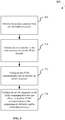
- FIG. 3 depicts a method 300 for JTAG lockout using the system of FIG. 1 , according to one embodiment.
- programming and test interface 102 retrieves the unlock sequence from embedded processor 104.
- the next step includes connecting the test interface to lockout processor 104 via the JTAG communication bus 120.
- step 306 we next configure the dual function JTAG communication bus 120 for transmission of the retrieved unlock sequence.
- the concluding step 308 includes validating the unlock sequence on the dual function JTAG communication bus 120, and allowing or disallowing JTAG communication to the programmable device(s) and/or embedded processor 104.
- Embodiments of the present invention provide a low cost, and flexible protection mechanism for JTAG protection.
- Most electronic units that require the use of JTAG have an existing processing element, and communication bus which can be used as is.
- One additional standard, low cost, configurable component is required to implement the lockout functionality.
- Embodiments do not rely on complicated encryption/decryption capabilities or complicated test rig capabilities.
Landscapes
- Engineering & Computer Science (AREA)
- Physics & Mathematics (AREA)
- General Physics & Mathematics (AREA)
- General Engineering & Computer Science (AREA)
- Software Systems (AREA)
- Theoretical Computer Science (AREA)
- Computer Security & Cryptography (AREA)
- Tests Of Electronic Circuits (AREA)
- Programmable Controllers (AREA)
- Test And Diagnosis Of Digital Computers (AREA)
Abstract
Description
- Exemplary embodiments pertain to the art of programmable device security, and particularly, to Joint Test Action Group (JTAG) lockout for embedded processor programming in a programmable device.
- The Institute of Electrical and Electronics Engineers (IEEE) provides industry Standard IEEE1149.1, commonly referred to as JTAG (which stands for Joint Test Action Group) communication. This standard details an industry set of commands that allow the JTAG user to read, modify, upload and download the program loaded into a programmable device. This access is a method for programming devices during production. For example, field programmable gate arrays (FPGAs), complex programmable logic device (CPLDs), memory devices, and many other types of processors can implement JTAG communication. Along with this capability comes the risk of undesired and/or malicious access to the programmable devices. Closed box access provided through JTAG (i.e., connecting to the device without directly accessing the physical programmable device itself) gives direct access to the control logic on the device with the ability to intentionality copy, or maliciously modify the operation of the device. Current JTAG security designs use complex encryption methodologies that require significant configuration control, key management, and complex testing rigs.
- Disclosed is a JTAG lockout assembly for a programmable device. The lockout assembly includes a programmable device having an embedded processor, and a lockout processor operatively connected to the embedded processor. The lockout processor has an unlock logic configured to allow or disallow a JTAG communication with the programmable device and/or embedded processor based on a unlock sequence operational across a dual function JTAG communication bus. The assembly also includes a test interface as a separate computer operatively connected to the embedded processor via a communication bus, that is removable after configuration of the system. The test interface is configured to retrieve the unlock sequence from one or more memory registers via an unlock controller operating on the test interface, and execute, via the unlock controller, the unlock sequence across the dual function JTAG communication bus. If the execution of the unlock sequence, which was retrieved from one or more predetermined memory registers located either on or off-device respective to the embedded processor, is determined to be valid by the lockout processor, the test interface can then access the programmable device through the JTAG.
- A Joint Test Action Group (JTAG) lockout processor is also disclosed. The processor connects a test interface to an embedded processor, receives a unlock sequence, validates the unlock sequence, and allows or disallows JTAG communication to one or more of the programmable device and the embedded processor.
- Also disclosed is a method for Joint Test Action Group (JTAG) lockout for a programmable device on an aircraft. The method includes connecting an embedded processor to a programmable device configured to control a portion of the aircraft. The method further includes configuring the lockout processor with an unlock logic configured that can allow or disallow JTAG communication with the via a dual function JTAG communication bus, and connecting a test interface to the programmable device and a lockout processor via a communication bus. The unlock channel is configured to transmit a unlock sequence across the communication bus. The method further includes configuring the lockout processor to allow or disallow the JTAG communication based on the unlock sequence.
- The following descriptions should not be considered limiting in any way. With reference to the accompanying drawings, like elements are numbered alike:
-
FIG. 1 depicts a system for JTAG lockout of programmable devices according to one embodiment; -
FIG. 2 depicts an exemplary implementation of the system ofFIG. 1 according to one embodiment; and -
FIG. 3 depicts a method for JTAG lockout using the system ofFIG. 1 according to one embodiment. - A detailed description of one or more embodiments of the disclosed apparatus and method are presented herein by way of exemplification and not limitation with reference to the Figures.
- Security features that do not rely on encryption for programming embedded processors or programmable devices may be advantageous when providing closed box access to the devices.
FIG. 1 depicts aJTAG lockout assembly 100 for locking out JTAG communication with embedded processors and/or programmable devices, according to one embodiment. Although not shown,system 100 is implemented on one or more systems on an aircraft, and provides JTAG security for programming the embedded processor without reliance on encryption that necessitates additional hardware and complexity in design. - Referring now to
FIG. 1 ,system 100 includes a programming and test interface 102 (hereafter "test interface 102" or "interface 102"), an embeddedprocessor 104, a JTAGlockout processor 106, andprogrammable devices Programmable devices processor 104 that are also isolated fromtest interface 102. -
Test interface 102 connects with embeddedprocessor 104 via acommunication bus 132 to retrieve all of the various portions of an unlock sequence that, when correctly executed, provide JTAG access to embeddedprocessor 104. Once allowed programming access to embeddedprocessor 104 orprogrammable devices 108 or 110 (by virtue of entry of a correct sequence)test interface 102 is permitted by JTAGlockout processor 106 to proceed JTAG communication with embeddedprocessor 104 for programming operations via JTAGcommunication line 120. The provided access allows for JTAG programming operations of embedded processor 104 (and any embedded processors and/or programmable devices connected devices) bytest interface 102. -
Programmable device 108 andprogrammable device 110 are operatively connected with embeddedprocessor 104 via the same JTAG bus.Protected bus 126 is protected by being isolated from programming andtest interface 102 by JTAG lockout processor. Embeddedprocessor 104 is connected to programming andtest interface 102 vialockout processor 106. After correct entry (execution) of the unlock sequence via the dual functionJTAG communication bus 120, programming andtest interface 102 may program any one or more of embeddedprocessor 104, programmable device 1 (shown as block 108) and programmable device 2 (shown as block 110). Although only three embedded processors are shown (that is, embeddedprocessor 104, and imbedded processors that are integrated withprogrammable device 108 and programmable device 110) it is appreciated that modern aircraft may have many programmable devices operatively connected together in various ways in one or more systems. -
Test interface 102 may be a computer, tablet, handheld device, or other processor operative for connecting to embedded devices and performing programming and/or testing steps with JTAG.Test interface 102 includes anunlock controller 105 configured to perform one or more operations described herein. In order to provide the capability for closed box access through JTAG,test interface 102 includes one or more features described herein that can protect against malicious access to critical systems to prevent updates, reconfiguration, or download of proprietary information and logic stored on embeddedprocessor 104,programmable device 108, and/orprogrammable device 110. -
Lockout processor 106 includes agate 116, andunlock logic 112 that can control access to protected bus 126 (and thus embeddedprocessor 104 and subsequently connecteddevices 108 and 110) viagate 116. Gate 116 may be any electronically operated gate, switch, etc., configured to allow and disallow data traffic to pass based on a control signal from a processor executing control logic (e.g., unlock logic 112). Examples of electronically operated gates include, for example, a MOSFET or other semiconductor or analog device.Unlock logic 112 is configured to controlgate 116 viagate bus 118. -
Memory 114 may be any operatively connected computer memory including, for example, a plurality of memory addresses in embeddedprocessor 104 or in lockout processor 106 (iflockout processor 106 is configured as an independent controller).Memory 114 may also be configured inlockout processor 106,devices test interface 102 by a device box 103).Memory 114 can include a plurality ofmemory registers memory 114 can vary, the locations of memory registers 126 - 130 are known by embeddedprocessor 104 andunlock logic 112, and thus, are predetermined. Knowledge of the specific locations of the memory registers 126 - 130 is protected by and known only to unlockcontroller 105. - Many electronic units used in aerospace include processing systems or programmable logic with closed box JTAG access. Modern aircraft include multiple embedded processing systems such as, for example, programmable gate arrays (FPGAs), complex programmable logic device (CPLDs), memory devices, and many processors. Programmable devices generally use JTAG communication for programming, which is always implemented via a communication bus directly connected to the programmable device. In one embodiment, one or more low cost and robust JTAG lockout features are provided that have low overhead costs for configuration and maintenance. Instead of configuring
system 100 with encryption that secures embeddedprocessor 104 from unwanted access,system 100 instead implements a multi bit programmable lockout feature. - Referring still to
FIG. 1 , embeddedprocessor 104 can be, for example, an aircraft system or sub-system (or portion thereof) for flight control, communication, etc., and may be encased in a housing (e.g., closed box) that provides access to the programmable device through a serial communication port configured to connect via acommunication bus 132, and JTAGcommunication line 120. -
Lockout processor 106 includes anunlock logic 112 configured to allow or disallow a JTAG communication with the embeddedprocessor 104 using JTAGcommunication channel 120 based on a unlock sequence. The unlock sequence is operational across the JTAGcommunication bus 120 as it functions as an unlock channel as one function of its dual functionality. For example, in one embodiment,system 100 transmits an unlock sequence across the JTAG communication bus 120 (as shown inFIG. 1 ). - Most programmable devices include a normal operation mode and a separate programming mode for programming the embedded processor. According to one embodiment,
JTAG lockout processor 106 provides accessibility to embeddedprocessor 104 only when in programming mode. In one embodiment, the operational mode is changed bytest interface 102 viacommunication bus 132 by causing a triggering event such as a device restart (power cycle), actuation of a mode switch (e.g., changing from operation mode to programming mode) or in some other way. Accordingly,test interface 102 can cause embeddedprocessor 104 to change an operational mode. - Embedded
processor 104 is configured to generate a unique lockout sequence at each change in the operational mode of the programmable device or any pre-defined event. For example, after each system restart, embeddedprocessor 104 generates a unique lockout sequence, which over-writes the previously saved lockout sequence stored in predetermined static memory location(s). In one embodiment, the lockout sequence changes based on a predefined event (like power up, read of a register, a power cycle, etc.). The sequence is different for every new JTAG access. As previously explained, the static memory locations are known only to embeddedprocessor 104 andJTAG lockout processor 106. - The unlock sequence includes a sequence portion indicative of one or more pulse sequences that are sequential with respect to a computer clock time. The pulse sequences are configured to pulse across the
JTAG communication bus 120. The pulse sequences may change at each triggering of a mode change, and are uniquely determined byJTAG lockout processor 106 at each triggering of the mode change. - According to one embodiment, unlock
logic 112 is configured to save the unlock sequence to one or more of a plurality of predeterminedmemory register locations 114. In one aspect, each of the predeterminedmemory register locations 114 can be configured to include a predetermined portion of the unlock sequence. For example, the predetermined portion can include only one of the sequence portion and the channel portion. In another aspect, a single memory register location may contain an entire unlock sequence. The location(s) are predetermined and known only tolockout processor 106. This feature provides a layer of security without encryption of the data. - According to one embodiment, when in normal operation mode,
test interface 102queries lockout processor 106 viacommunication bus 132 for the unlock sequence from a specific, known, private address such as, for example,address register 130. After retrieving the unlock sequence, unlockcontroller 105 may transmit (execute) the retrieved sequences over theJTAG communication bus 120. - An exemplary unlock sequence includes two portions: the unlock sequence may be a series of pulses with respect to time. For example, the unlock sequence may be four sequential pulses, followed by two cycles of no pulses, then a single pulse on the
JTAG communication bus 120. According to this example, afterunlock controller 105 has retrieved the saved unlock sequence portions from embeddedprocessor 104, unlockcontroller 105 may execute the retrieved sequences across theJTAG communication bus 120. Accordingly,JTAG lockout processor 106 receives, via theJTAG communication bus 120, four sequential pulses, followed by two cycles of no pulses, then a single pulse. Any combination of pulses, channels, and time diminutions are contemplated. According to the present example, the unlock sequence includes the pulses in a particular order, and at a particular rate with respect to computer clock cycle time. The number of pulses and the time portion may be determined based on a random number generator that is triggered at each mode change of embeddedprocessor 104 and/orlockout processor 106. There are many known ways to generate a random number including, for example, a number generation algorithm, a number generator chip, etc. Accordingly,test interface 102 may retrieve, viaunlock controller 105, the unlock sequence from one or more memory registers 114, and execute, vialockout processor 106, the unlock sequence.Lockout processor 106 may provide or deny access to programmable device (e.g., embedded processor 104) responsive to testinterface 102 executing the unlock sequence across theJTAG communication bus 120. - It is again emphasized that the precise location(s) for storing unlock sequences are known only to embedded
processor 104 andtest interface 102. Although the specific lockout or access is controlled by the unlock sequence that changes at each mode change (startup for example), the location at which they are stored is not changed. -
FIG. 2 depicts an exemplary implementation of operation of the system ofFIG. 1 , according to one embodiment. Referring now toFIG. 2 ,mode trigger 202 depicts a starting low power operational mode that transitions into a normal operational mode. As shown on the subsequent line depicting data transmission oncommunication bus 132,test interface 102 retrieves anunlock sequence 206.Unlock sequence 206 includes thesequence portion 210 indicative of one ormore pulse sequences FIG. 2 ) the number prior to the ":" is the number of clock periods for the first pulse on theJTAG communication bus 120 and the number to the right of ":" is the number of clock periods for the second pulse on theJTAG communication bus 120. Although only two pulse sequences are shown, it is appreciated that three, four, five, or more pulse sequence patterns are contemplated. For example, theunlock sequence 206 could have 3, 4, 5, or more numbers where each number represents the next pulse duration. In another aspect, the pulse pattern could alternate between length of high/low periods, etc. The syntax ofunlock sequence 206 is exemplary only, and not intended to be a limiting feature to embodiments described herein. - As shown in the
JTAG Enable line 212, once the third pulse is complete on channel 124 (the final portion of unlock sequence 206), unlocklogic 112 determines whether the unlock sequence executed bytest interface 102 is valid. Determining whether the sequence is valid includes comparing the executed sequence fromtest interface 102 with the last stored sequences in memory. As demonstrated inFIG. 2 , the execution of the unlock sequence was determined to be valid, and thus, JTAG enableline 212 shows a gate closing 214 (e.g., gate 116). The gate closing is effectuated byunlock logic 112 viagate bus 118. JTAG communication is now allowed viaJTAG communication line 120.Gate 116 is opened byunlock logic 112 after cessation of JTAG communication, or subsequent to a mode change. - Demonstrating a second generation of a unique unlock sequence, subsequent to another mode change, a
unique unlock sequence 216 is generated byJTAG lockout processor 106 having three pulses on theJTAG communication bus 120. After receipt of a valid execution of this sequence,JTAG lockout processor 106 closesgate 116 and access is permitted (enabled 218) to embeddedprocessor 104. Now JTAG programming operations are allowed. -
FIG. 3 depicts amethod 300 for JTAG lockout using the system ofFIG. 1 , according to one embodiment. Referring briefly toFIG. 3 , as shown inblock 302, programming andtest interface 102 retrieves the unlock sequence from embeddedprocessor 104. - As shown in
block 304, the next step includes connecting the test interface tolockout processor 104 via theJTAG communication bus 120. - In
step 306, we next configure the dual functionJTAG communication bus 120 for transmission of the retrieved unlock sequence. - The concluding
step 308 includes validating the unlock sequence on the dual functionJTAG communication bus 120, and allowing or disallowing JTAG communication to the programmable device(s) and/or embeddedprocessor 104. - Embodiments of the present invention provide a low cost, and flexible protection mechanism for JTAG protection. Most electronic units that require the use of JTAG have an existing processing element, and communication bus which can be used as is. One additional standard, low cost, configurable component is required to implement the lockout functionality. Embodiments do not rely on complicated encryption/decryption capabilities or complicated test rig capabilities.
- The term "about" is intended to include the degree of error associated with measurement of the particular quantity based upon the equipment available at the time of filing the application. For example, "about" can include a range of ± 8% or 5%, or 2% of a given value.
- The terminology used herein is for the purpose of describing particular embodiments only and is not intended to be limiting of the present disclosure. As used herein, the singular forms "a", "an" and "the" are intended to include the plural forms as well, unless the context clearly indicates otherwise. It will be further understood that the terms "comprises" and/or "comprising," when used in this specification, specify the presence of stated features, integers, steps, operations, elements, and/or components, but do not preclude the presence or addition of one or more other features, integers, steps, operations, element components, and/or groups thereof.
- While the present disclosure has been described with reference to an exemplary embodiment or embodiments, it will be understood by those skilled in the art that various changes may be made and equivalents may be substituted for elements thereof without departing from the scope of the present invention as defined by the claims. In addition, many modifications may be made to adapt a particular situation or material to the teachings of the present disclosure without departing from the scope of the invention. Therefore, it is intended that the present disclosure not be limited to the particular embodiment disclosed as the best mode contemplated for carrying out this present disclosure, but that the invention is defined by the scope of the claims.
Claims (12)
- A Joint Test Action Group (JTAG) lockout assembly for a programmable device comprising:an embedded processor (104) in the programmable device (108);a lockout processor (106) operatively connected to the embedded processor, wherein the lockout processor comprises an unlock logic (112) configured to allow or disallow JTAG communication with the embedded processor based on an unlock sequence operational across a dual function JTAG communication bus (120); anda test interface (102) operatively connected to the embedded processor and the lockout processor, the test interface configured to cause an unlock controller to:retrieve an unlock sequence on the JTAG communication bus from one or more memory registers via a lockout controller operating on the test interface; andexecute the unlock sequence across the JTAG communication bus; andaccess the programmable device through the JTAG communication bus responsive to executing the unlock sequence.
- The JTAG lockout assembly of claim 1, wherein the JTAG communication bus (120) is configured for dual functions comprising JTAG communication and unlock communication.
- The JTAG lockout assembly of claim 1 or 2, wherein the lockout processor comprises:
unlock logic (112) configured to:validate the unlock sequence based on an operational mode change; anda gate (116) operatively connected to the unlock logic and configured to connect the JTAG communication bus with the programmable device when the test interface has executed a valid unlock sequence. - The JTAG lockout assembly of claim 3, wherein the embedded processor is configured to generate a unique lockout sequence at each change in the operational mode of the programmable device.
- The JTAG lockout assembly of claim 3 or 4, wherein the unlock logic is configured to save the unlock sequence to a predetermined memory register location.
- The JTAG lockout assembly of claim 3, 4 or 5, wherein the unlock sequence comprises a sequence portion indicative of one or more pulse sequences that are sequential with respect to a computer clock time.
- The JTAG lockout assembly of claim 2, wherein the unlock sequence is saved to a plurality of predetermined memory register locations, wherein each of the predetermined memory register locations comprises a predetermined portion of the unlock sequence.
- The JTAG lockout assembly of any preceding claim, further comprising a second programmable device (110) operatively connected to the embedded processor and the lockout processor, wherein the lockout processor allows JTAG communication with the second programmable device responsive to the test interface executing the unlock sequence.
- A method for Joint Test Action Group (JTAG) lockout for a programmable device on an aircraft comprising:connecting a lockout processor to an embedded processor in a programmable device configured to control a portion of the aircraft;configuring the lockout processor with an unlock logic configured that can allow or disallow JTAG communication with the a JTAG communication bus; andconnecting a test interface to the programmable device and a lockout processor via a JTAG communication bus.
- The method of claim 9, further comprising:configuring the embedded processor to create a unique unlock sequence responsive to a change in an operational mode of the programmable device; andconfiguring the test interface with a lockout controller for:retrieving the unlock sequence from one or more memory registers;executing the unlock sequence across the JTAG bus andaccessing the programmable device responsive to a valid execution the unlock sequence.
- The method of claim 9, further comprising configuring the embedded processor to generate a unique lockout sequence at each change in the operational mode of the programmable device.
- The method of claim 9, further comprising connecting the unlock logic to a plurality of memory registers and configuring the unlock logic to save the unlock sequence to a predetermined memory register location at each change in the operational mode of the programmable device.
Applications Claiming Priority (1)
| Application Number | Priority Date | Filing Date | Title |
|---|---|---|---|
| US15/914,121 US10540213B2 (en) | 2018-03-07 | 2018-03-07 | JTAG lockout with dual function communication channels |
Publications (2)
| Publication Number | Publication Date |
|---|---|
| EP3540450A1 true EP3540450A1 (en) | 2019-09-18 |
| EP3540450B1 EP3540450B1 (en) | 2022-10-19 |
Family
ID=65717878
Family Applications (1)
| Application Number | Title | Priority Date | Filing Date |
|---|---|---|---|
| EP19160997.3A Active EP3540450B1 (en) | 2018-03-07 | 2019-03-06 | Jtag lockout with dual function communication channels |
Country Status (2)
| Country | Link |
|---|---|
| US (1) | US10540213B2 (en) |
| EP (1) | EP3540450B1 (en) |
Citations (3)
| Publication number | Priority date | Publication date | Assignee | Title |
|---|---|---|---|---|
| US20120060067A1 (en) * | 2008-12-17 | 2012-03-08 | Samsung Electronics Co., Ltd. | Apparatus and method of authenticating joint test action group (jtag) |
| US8438436B1 (en) * | 2010-06-04 | 2013-05-07 | Xilinx, Inc. | Secure design-for-test scan chains |
| US20150349968A1 (en) * | 2014-03-23 | 2015-12-03 | Southern Methodist University | Protecting Hidden Content In Integrated Circuits |
Family Cites Families (16)
| Publication number | Priority date | Publication date | Assignee | Title |
|---|---|---|---|---|
| US7171542B1 (en) * | 2000-06-19 | 2007-01-30 | Silicon Labs Cp, Inc. | Reconfigurable interface for coupling functional input/output blocks to limited number of i/o pins |
| US6983441B2 (en) | 2002-06-28 | 2006-01-03 | Texas Instruments Incorporated | Embedding a JTAG host controller into an FPGA design |
| US7313730B1 (en) * | 2004-05-20 | 2007-12-25 | Xilinx, Inc. | Configuration logic for embedded software |
| US7685418B1 (en) | 2005-01-19 | 2010-03-23 | Altera Corporation | Mechanisms and techniques for protecting intellectual property |
| US7657807B1 (en) | 2005-06-27 | 2010-02-02 | Sun Microsystems, Inc. | Integrated circuit with embedded test functionality |
| US7363564B2 (en) | 2005-07-15 | 2008-04-22 | Seagate Technology Llc | Method and apparatus for securing communications ports in an electronic device |
| US20070162759A1 (en) * | 2005-12-28 | 2007-07-12 | Motorola, Inc. | Protected port for electronic access to an embedded device |
| US7844997B2 (en) * | 2006-01-12 | 2010-11-30 | Honeywell International Inc. | Securing standard test access port with an independent security key interface |
| US8099629B2 (en) * | 2006-07-14 | 2012-01-17 | Marvell World Trade Ltd. | System-on-a-chip (SoC) test interface security |
| US8356361B2 (en) * | 2006-11-07 | 2013-01-15 | Spansion Llc | Secure co-processing memory controller integrated into an embedded memory subsystem |
| US9564902B2 (en) * | 2007-04-17 | 2017-02-07 | Cypress Semiconductor Corporation | Dynamically configurable and re-configurable data path |
| US7886150B2 (en) * | 2007-05-11 | 2011-02-08 | Mips Technologies, Inc. | System debug and trace system and method, and applications thereof |
| US7906983B2 (en) | 2008-12-08 | 2011-03-15 | Intuitive Research And Technology | Programmable logic device having an embedded test logic with secure access control |
| US9262340B1 (en) * | 2011-12-29 | 2016-02-16 | Cypress Semiconductor Corporation | Privileged mode methods and circuits for processor systems |
| US9224012B2 (en) * | 2013-05-20 | 2015-12-29 | Advanced Micro Devices, Inc. | Debug functionality in a secure computing environment |
| US20170090909A1 (en) * | 2015-09-25 | 2017-03-30 | Qualcomm Incorporated | Secure patch updates for programmable memories |
-
2018
- 2018-03-07 US US15/914,121 patent/US10540213B2/en active Active
-
2019
- 2019-03-06 EP EP19160997.3A patent/EP3540450B1/en active Active
Patent Citations (3)
| Publication number | Priority date | Publication date | Assignee | Title |
|---|---|---|---|---|
| US20120060067A1 (en) * | 2008-12-17 | 2012-03-08 | Samsung Electronics Co., Ltd. | Apparatus and method of authenticating joint test action group (jtag) |
| US8438436B1 (en) * | 2010-06-04 | 2013-05-07 | Xilinx, Inc. | Secure design-for-test scan chains |
| US20150349968A1 (en) * | 2014-03-23 | 2015-12-03 | Southern Methodist University | Protecting Hidden Content In Integrated Circuits |
Non-Patent Citations (1)
| Title |
|---|
| CLARK C J: "Anti-tamper JTAG TAP design enables DRM to JTAG registers and P1687 on-chip instruments", HARDWARE-ORIENTED SECURITY AND TRUST (HOST), 2010 IEEE INTERNATIONAL SYMPOSIUM ON, IEEE, PISCATAWAY, NJ, USA, 13 June 2010 (2010-06-13), pages 19 - 24, XP031710173, ISBN: 978-1-4244-7811-8 * |
Also Published As
| Publication number | Publication date |
|---|---|
| US10540213B2 (en) | 2020-01-21 |
| US20190278633A1 (en) | 2019-09-12 |
| EP3540450B1 (en) | 2022-10-19 |
Similar Documents
| Publication | Publication Date | Title |
|---|---|---|
| EP3385736B1 (en) | Jtag lockout for embedded processors in programmable devices | |
| KR100977675B1 (en) | Integrated circuit security and how | |
| US6304970B1 (en) | Hardware access control locking | |
| EP1499906B1 (en) | Method and apparatus for secure scan testing | |
| EP2973198B1 (en) | Integrated circuit with parts activated based on intrinsic features | |
| US10305679B2 (en) | Method for implementing a communication between control units | |
| US8341475B2 (en) | Microprocessor comprising signature means for detecting an attack by error injection | |
| US20070237325A1 (en) | Method and apparatus to improve security of cryptographic systems | |
| US20110145934A1 (en) | Autonomous distributed programmable logic for monitoring and securing electronic systems | |
| US10107855B1 (en) | Electromagnetic verification of integrated circuits | |
| US10762177B2 (en) | Method for preventing an unauthorized operation of a motor vehicle | |
| US10025954B2 (en) | Method for operating a control unit | |
| EP2384482A1 (en) | Method, system and integrated circuit for enabling access to a memory element | |
| US8438436B1 (en) | Secure design-for-test scan chains | |
| US8896346B1 (en) | Self-modifying FPGA for anti-tamper applications | |
| EP3540450B1 (en) | Jtag lockout with dual function communication channels | |
| US11347837B2 (en) | Method and apparatus for enhancing security of vehicle controller | |
| JP2020072431A (en) | Control device | |
| US20160116893A1 (en) | Autonomous control systems and methods | |
| US9483665B2 (en) | Method for monitoring an electronic security module | |
| US7398441B1 (en) | System and method for providing secure boundary scan interface access | |
| US20150324610A1 (en) | Method for managing software functionalities in a control unit | |
| Kalligeros et al. | Oracle-based logic locking attacks: Protect the oracle not only the netlist | |
| US20230109011A1 (en) | Placing a device in secure mode | |
| US10289872B2 (en) | Secure mechanism for finite provisioning of an integrated circuit |
Legal Events
| Date | Code | Title | Description |
|---|---|---|---|
| PUAI | Public reference made under article 153(3) epc to a published international application that has entered the european phase |
Free format text: ORIGINAL CODE: 0009012 |
|
| STAA | Information on the status of an ep patent application or granted ep patent |
Free format text: STATUS: THE APPLICATION HAS BEEN PUBLISHED |
|
| AK | Designated contracting states |
Kind code of ref document: A1 Designated state(s): AL AT BE BG CH CY CZ DE DK EE ES FI FR GB GR HR HU IE IS IT LI LT LU LV MC MK MT NL NO PL PT RO RS SE SI SK SM TR |
|
| AX | Request for extension of the european patent |
Extension state: BA ME |
|
| STAA | Information on the status of an ep patent application or granted ep patent |
Free format text: STATUS: REQUEST FOR EXAMINATION WAS MADE |
|
| 17P | Request for examination filed |
Effective date: 20191216 |
|
| RBV | Designated contracting states (corrected) |
Designated state(s): AL AT BE BG CH CY CZ DE DK EE ES FI FR GB GR HR HU IE IS IT LI LT LU LV MC MK MT NL NO PL PT RO RS SE SI SK SM TR |
|
| GRAP | Despatch of communication of intention to grant a patent |
Free format text: ORIGINAL CODE: EPIDOSNIGR1 |
|
| STAA | Information on the status of an ep patent application or granted ep patent |
Free format text: STATUS: GRANT OF PATENT IS INTENDED |
|
| INTG | Intention to grant announced |
Effective date: 20220509 |
|
| GRAS | Grant fee paid |
Free format text: ORIGINAL CODE: EPIDOSNIGR3 |
|
| GRAA | (expected) grant |
Free format text: ORIGINAL CODE: 0009210 |
|
| STAA | Information on the status of an ep patent application or granted ep patent |
Free format text: STATUS: THE PATENT HAS BEEN GRANTED |
|
| AK | Designated contracting states |
Kind code of ref document: B1 Designated state(s): AL AT BE BG CH CY CZ DE DK EE ES FI FR GB GR HR HU IE IS IT LI LT LU LV MC MK MT NL NO PL PT RO RS SE SI SK SM TR |
|
| REG | Reference to a national code |
Ref country code: GB Ref legal event code: FG4D |
|
| REG | Reference to a national code |
Ref country code: CH Ref legal event code: EP |
|
| REG | Reference to a national code |
Ref country code: DE Ref legal event code: R096 Ref document number: 602019020704 Country of ref document: DE |
|
| REG | Reference to a national code |
Ref country code: IE Ref legal event code: FG4D |
|
| REG | Reference to a national code |
Ref country code: AT Ref legal event code: REF Ref document number: 1525878 Country of ref document: AT Kind code of ref document: T Effective date: 20221115 |
|
| REG | Reference to a national code |
Ref country code: LT Ref legal event code: MG9D |
|
| REG | Reference to a national code |
Ref country code: NL Ref legal event code: MP Effective date: 20221019 |
|
| REG | Reference to a national code |
Ref country code: AT Ref legal event code: MK05 Ref document number: 1525878 Country of ref document: AT Kind code of ref document: T Effective date: 20221019 |
|
| PG25 | Lapsed in a contracting state [announced via postgrant information from national office to epo] |
Ref country code: NL Free format text: LAPSE BECAUSE OF FAILURE TO SUBMIT A TRANSLATION OF THE DESCRIPTION OR TO PAY THE FEE WITHIN THE PRESCRIBED TIME-LIMIT Effective date: 20221019 |
|
| PG25 | Lapsed in a contracting state [announced via postgrant information from national office to epo] |
Ref country code: SE Free format text: LAPSE BECAUSE OF FAILURE TO SUBMIT A TRANSLATION OF THE DESCRIPTION OR TO PAY THE FEE WITHIN THE PRESCRIBED TIME-LIMIT Effective date: 20221019 Ref country code: PT Free format text: LAPSE BECAUSE OF FAILURE TO SUBMIT A TRANSLATION OF THE DESCRIPTION OR TO PAY THE FEE WITHIN THE PRESCRIBED TIME-LIMIT Effective date: 20230220 Ref country code: NO Free format text: LAPSE BECAUSE OF FAILURE TO SUBMIT A TRANSLATION OF THE DESCRIPTION OR TO PAY THE FEE WITHIN THE PRESCRIBED TIME-LIMIT Effective date: 20230119 Ref country code: LT Free format text: LAPSE BECAUSE OF FAILURE TO SUBMIT A TRANSLATION OF THE DESCRIPTION OR TO PAY THE FEE WITHIN THE PRESCRIBED TIME-LIMIT Effective date: 20221019 Ref country code: FI Free format text: LAPSE BECAUSE OF FAILURE TO SUBMIT A TRANSLATION OF THE DESCRIPTION OR TO PAY THE FEE WITHIN THE PRESCRIBED TIME-LIMIT Effective date: 20221019 Ref country code: ES Free format text: LAPSE BECAUSE OF FAILURE TO SUBMIT A TRANSLATION OF THE DESCRIPTION OR TO PAY THE FEE WITHIN THE PRESCRIBED TIME-LIMIT Effective date: 20221019 Ref country code: AT Free format text: LAPSE BECAUSE OF FAILURE TO SUBMIT A TRANSLATION OF THE DESCRIPTION OR TO PAY THE FEE WITHIN THE PRESCRIBED TIME-LIMIT Effective date: 20221019 |
|
| PG25 | Lapsed in a contracting state [announced via postgrant information from national office to epo] |
Ref country code: RS Free format text: LAPSE BECAUSE OF FAILURE TO SUBMIT A TRANSLATION OF THE DESCRIPTION OR TO PAY THE FEE WITHIN THE PRESCRIBED TIME-LIMIT Effective date: 20221019 Ref country code: PL Free format text: LAPSE BECAUSE OF FAILURE TO SUBMIT A TRANSLATION OF THE DESCRIPTION OR TO PAY THE FEE WITHIN THE PRESCRIBED TIME-LIMIT Effective date: 20221019 Ref country code: LV Free format text: LAPSE BECAUSE OF FAILURE TO SUBMIT A TRANSLATION OF THE DESCRIPTION OR TO PAY THE FEE WITHIN THE PRESCRIBED TIME-LIMIT Effective date: 20221019 Ref country code: IS Free format text: LAPSE BECAUSE OF FAILURE TO SUBMIT A TRANSLATION OF THE DESCRIPTION OR TO PAY THE FEE WITHIN THE PRESCRIBED TIME-LIMIT Effective date: 20230219 Ref country code: HR Free format text: LAPSE BECAUSE OF FAILURE TO SUBMIT A TRANSLATION OF THE DESCRIPTION OR TO PAY THE FEE WITHIN THE PRESCRIBED TIME-LIMIT Effective date: 20221019 Ref country code: GR Free format text: LAPSE BECAUSE OF FAILURE TO SUBMIT A TRANSLATION OF THE DESCRIPTION OR TO PAY THE FEE WITHIN THE PRESCRIBED TIME-LIMIT Effective date: 20230120 |
|
| P01 | Opt-out of the competence of the unified patent court (upc) registered |
Effective date: 20230522 |
|
| REG | Reference to a national code |
Ref country code: DE Ref legal event code: R097 Ref document number: 602019020704 Country of ref document: DE |
|
| PG25 | Lapsed in a contracting state [announced via postgrant information from national office to epo] |
Ref country code: SM Free format text: LAPSE BECAUSE OF FAILURE TO SUBMIT A TRANSLATION OF THE DESCRIPTION OR TO PAY THE FEE WITHIN THE PRESCRIBED TIME-LIMIT Effective date: 20221019 Ref country code: RO Free format text: LAPSE BECAUSE OF FAILURE TO SUBMIT A TRANSLATION OF THE DESCRIPTION OR TO PAY THE FEE WITHIN THE PRESCRIBED TIME-LIMIT Effective date: 20221019 Ref country code: EE Free format text: LAPSE BECAUSE OF FAILURE TO SUBMIT A TRANSLATION OF THE DESCRIPTION OR TO PAY THE FEE WITHIN THE PRESCRIBED TIME-LIMIT Effective date: 20221019 Ref country code: DK Free format text: LAPSE BECAUSE OF FAILURE TO SUBMIT A TRANSLATION OF THE DESCRIPTION OR TO PAY THE FEE WITHIN THE PRESCRIBED TIME-LIMIT Effective date: 20221019 Ref country code: CZ Free format text: LAPSE BECAUSE OF FAILURE TO SUBMIT A TRANSLATION OF THE DESCRIPTION OR TO PAY THE FEE WITHIN THE PRESCRIBED TIME-LIMIT Effective date: 20221019 |
|
| PLBE | No opposition filed within time limit |
Free format text: ORIGINAL CODE: 0009261 |
|
| STAA | Information on the status of an ep patent application or granted ep patent |
Free format text: STATUS: NO OPPOSITION FILED WITHIN TIME LIMIT |
|
| PG25 | Lapsed in a contracting state [announced via postgrant information from national office to epo] |
Ref country code: SK Free format text: LAPSE BECAUSE OF FAILURE TO SUBMIT A TRANSLATION OF THE DESCRIPTION OR TO PAY THE FEE WITHIN THE PRESCRIBED TIME-LIMIT Effective date: 20221019 Ref country code: AL Free format text: LAPSE BECAUSE OF FAILURE TO SUBMIT A TRANSLATION OF THE DESCRIPTION OR TO PAY THE FEE WITHIN THE PRESCRIBED TIME-LIMIT Effective date: 20221019 |
|
| 26N | No opposition filed |
Effective date: 20230720 |
|
| PG25 | Lapsed in a contracting state [announced via postgrant information from national office to epo] |
Ref country code: MC Free format text: LAPSE BECAUSE OF FAILURE TO SUBMIT A TRANSLATION OF THE DESCRIPTION OR TO PAY THE FEE WITHIN THE PRESCRIBED TIME-LIMIT Effective date: 20221019 |
|
| REG | Reference to a national code |
Ref country code: CH Ref legal event code: PL |
|
| PG25 | Lapsed in a contracting state [announced via postgrant information from national office to epo] |
Ref country code: SI Free format text: LAPSE BECAUSE OF FAILURE TO SUBMIT A TRANSLATION OF THE DESCRIPTION OR TO PAY THE FEE WITHIN THE PRESCRIBED TIME-LIMIT Effective date: 20221019 |
|
| REG | Reference to a national code |
Ref country code: BE Ref legal event code: MM Effective date: 20230331 |
|
| PG25 | Lapsed in a contracting state [announced via postgrant information from national office to epo] |
Ref country code: LU Free format text: LAPSE BECAUSE OF NON-PAYMENT OF DUE FEES Effective date: 20230306 |
|
| REG | Reference to a national code |
Ref country code: IE Ref legal event code: MM4A |
|
| PG25 | Lapsed in a contracting state [announced via postgrant information from national office to epo] |
Ref country code: LI Free format text: LAPSE BECAUSE OF NON-PAYMENT OF DUE FEES Effective date: 20230331 Ref country code: IE Free format text: LAPSE BECAUSE OF NON-PAYMENT OF DUE FEES Effective date: 20230306 Ref country code: CH Free format text: LAPSE BECAUSE OF NON-PAYMENT OF DUE FEES Effective date: 20230331 |
|
| PG25 | Lapsed in a contracting state [announced via postgrant information from national office to epo] |
Ref country code: BE Free format text: LAPSE BECAUSE OF NON-PAYMENT OF DUE FEES Effective date: 20230331 |
|
| PG25 | Lapsed in a contracting state [announced via postgrant information from national office to epo] |
Ref country code: IT Free format text: LAPSE BECAUSE OF FAILURE TO SUBMIT A TRANSLATION OF THE DESCRIPTION OR TO PAY THE FEE WITHIN THE PRESCRIBED TIME-LIMIT Effective date: 20221019 |
|
| PG25 | Lapsed in a contracting state [announced via postgrant information from national office to epo] |
Ref country code: BG Free format text: LAPSE BECAUSE OF FAILURE TO SUBMIT A TRANSLATION OF THE DESCRIPTION OR TO PAY THE FEE WITHIN THE PRESCRIBED TIME-LIMIT Effective date: 20221019 |
|
| PG25 | Lapsed in a contracting state [announced via postgrant information from national office to epo] |
Ref country code: BG Free format text: LAPSE BECAUSE OF FAILURE TO SUBMIT A TRANSLATION OF THE DESCRIPTION OR TO PAY THE FEE WITHIN THE PRESCRIBED TIME-LIMIT Effective date: 20221019 |
|
| PG25 | Lapsed in a contracting state [announced via postgrant information from national office to epo] |
Ref country code: CY Free format text: LAPSE BECAUSE OF FAILURE TO SUBMIT A TRANSLATION OF THE DESCRIPTION OR TO PAY THE FEE WITHIN THE PRESCRIBED TIME-LIMIT; INVALID AB INITIO Effective date: 20190306 |
|
| PG25 | Lapsed in a contracting state [announced via postgrant information from national office to epo] |
Ref country code: HU Free format text: LAPSE BECAUSE OF FAILURE TO SUBMIT A TRANSLATION OF THE DESCRIPTION OR TO PAY THE FEE WITHIN THE PRESCRIBED TIME-LIMIT; INVALID AB INITIO Effective date: 20190306 |
|
| PG25 | Lapsed in a contracting state [announced via postgrant information from national office to epo] |
Ref country code: TR Free format text: LAPSE BECAUSE OF FAILURE TO SUBMIT A TRANSLATION OF THE DESCRIPTION OR TO PAY THE FEE WITHIN THE PRESCRIBED TIME-LIMIT Effective date: 20221019 |
|
| PGFP | Annual fee paid to national office [announced via postgrant information from national office to epo] |
Ref country code: GB Payment date: 20260219 Year of fee payment: 8 |
|
| PGFP | Annual fee paid to national office [announced via postgrant information from national office to epo] |
Ref country code: DE Payment date: 20260219 Year of fee payment: 8 |
|
| PGFP | Annual fee paid to national office [announced via postgrant information from national office to epo] |
Ref country code: FR Payment date: 20260219 Year of fee payment: 8 |