EP3537610A2 - Hybrid half/quarter-rate decision feedback equalizer and display including hybrid half/quarter-rate decision feedback equalizer - Google Patents
Hybrid half/quarter-rate decision feedback equalizer and display including hybrid half/quarter-rate decision feedback equalizer Download PDFInfo
- Publication number
- EP3537610A2 EP3537610A2 EP19160874.4A EP19160874A EP3537610A2 EP 3537610 A2 EP3537610 A2 EP 3537610A2 EP 19160874 A EP19160874 A EP 19160874A EP 3537610 A2 EP3537610 A2 EP 3537610A2
- Authority
- EP
- European Patent Office
- Prior art keywords
- clock
- stage
- decision feedback
- phase
- feedback equalizer
- Prior art date
- Legal status (The legal status is an assumption and is not a legal conclusion. Google has not performed a legal analysis and makes no representation as to the accuracy of the status listed.)
- Ceased
Links
- 230000000630 rising effect Effects 0.000 claims description 15
- 230000000295 complement effect Effects 0.000 claims description 12
- 230000007704 transition Effects 0.000 claims description 8
- 229910044991 metal oxide Inorganic materials 0.000 claims description 7
- 150000004706 metal oxides Chemical class 0.000 claims description 7
- 239000004065 semiconductor Substances 0.000 claims description 7
- 239000004020 conductor Substances 0.000 description 8
- 238000010586 diagram Methods 0.000 description 5
- 238000006243 chemical reaction Methods 0.000 description 2
- 230000000694 effects Effects 0.000 description 2
- 238000011084 recovery Methods 0.000 description 2
- 230000014509 gene expression Effects 0.000 description 1
- 238000012986 modification Methods 0.000 description 1
- 230000004048 modification Effects 0.000 description 1
Images

Classifications
-
- H—ELECTRICITY
- H04—ELECTRIC COMMUNICATION TECHNIQUE
- H04L—TRANSMISSION OF DIGITAL INFORMATION, e.g. TELEGRAPHIC COMMUNICATION
- H04L25/00—Baseband systems
- H04L25/02—Details ; arrangements for supplying electrical power along data transmission lines
- H04L25/03—Shaping networks in transmitter or receiver, e.g. adaptive shaping networks
- H04L25/03006—Arrangements for removing intersymbol interference
- H04L25/03178—Arrangements involving sequence estimation techniques
- H04L25/03248—Arrangements for operating in conjunction with other apparatus
- H04L25/03254—Operation with other circuitry for removing intersymbol interference
- H04L25/03267—Operation with other circuitry for removing intersymbol interference with decision feedback equalisers
-
- G—PHYSICS
- G09—EDUCATION; CRYPTOGRAPHY; DISPLAY; ADVERTISING; SEALS
- G09G—ARRANGEMENTS OR CIRCUITS FOR CONTROL OF INDICATING DEVICES USING STATIC MEANS TO PRESENT VARIABLE INFORMATION
- G09G3/00—Control arrangements or circuits, of interest only in connection with visual indicators other than cathode-ray tubes
- G09G3/20—Control arrangements or circuits, of interest only in connection with visual indicators other than cathode-ray tubes for presentation of an assembly of a number of characters, e.g. a page, by composing the assembly by combination of individual elements arranged in a matrix no fixed position being assigned to or needed to be assigned to the individual characters or partial characters
-
- H—ELECTRICITY
- H03—ELECTRONIC CIRCUITRY
- H03D—DEMODULATION OR TRANSFERENCE OF MODULATION FROM ONE CARRIER TO ANOTHER
- H03D7/00—Transference of modulation from one carrier to another, e.g. frequency-changing
- H03D7/14—Balanced arrangements
- H03D7/1425—Balanced arrangements with transistors
- H03D7/1441—Balanced arrangements with transistors using field-effect transistors
-
- H—ELECTRICITY
- H03—ELECTRONIC CIRCUITRY
- H03K—PULSE TECHNIQUE
- H03K19/00—Logic circuits, i.e. having at least two inputs acting on one output; Inverting circuits
- H03K19/0008—Arrangements for reducing power consumption
-
- H—ELECTRICITY
- H03—ELECTRONIC CIRCUITRY
- H03K—PULSE TECHNIQUE
- H03K19/00—Logic circuits, i.e. having at least two inputs acting on one output; Inverting circuits
- H03K19/02—Logic circuits, i.e. having at least two inputs acting on one output; Inverting circuits using specified components
- H03K19/08—Logic circuits, i.e. having at least two inputs acting on one output; Inverting circuits using specified components using semiconductor devices
- H03K19/094—Logic circuits, i.e. having at least two inputs acting on one output; Inverting circuits using specified components using semiconductor devices using field-effect transistors
- H03K19/09432—Logic circuits, i.e. having at least two inputs acting on one output; Inverting circuits using specified components using semiconductor devices using field-effect transistors with coupled sources or source coupled logic
-
- H—ELECTRICITY
- H03—ELECTRONIC CIRCUITRY
- H03K—PULSE TECHNIQUE
- H03K3/00—Circuits for generating electric pulses; Monostable, bistable or multistable circuits
- H03K3/02—Generators characterised by the type of circuit or by the means used for producing pulses
- H03K3/353—Generators characterised by the type of circuit or by the means used for producing pulses by the use, as active elements, of field-effect transistors with internal or external positive feedback
- H03K3/356—Bistable circuits
- H03K3/356104—Bistable circuits using complementary field-effect transistors
- H03K3/356113—Bistable circuits using complementary field-effect transistors using additional transistors in the input circuit
- H03K3/35613—Bistable circuits using complementary field-effect transistors using additional transistors in the input circuit the input circuit having a differential configuration
-
- H—ELECTRICITY
- H03—ELECTRONIC CIRCUITRY
- H03M—CODING; DECODING; CODE CONVERSION IN GENERAL
- H03M9/00—Parallel/series conversion or vice versa
-
- H—ELECTRICITY
- H04—ELECTRIC COMMUNICATION TECHNIQUE
- H04L—TRANSMISSION OF DIGITAL INFORMATION, e.g. TELEGRAPHIC COMMUNICATION
- H04L25/00—Baseband systems
- H04L25/02—Details ; arrangements for supplying electrical power along data transmission lines
- H04L25/0264—Arrangements for coupling to transmission lines
- H04L25/0272—Arrangements for coupling to multiple lines, e.g. for differential transmission
-
- H—ELECTRICITY
- H04—ELECTRIC COMMUNICATION TECHNIQUE
- H04L—TRANSMISSION OF DIGITAL INFORMATION, e.g. TELEGRAPHIC COMMUNICATION
- H04L25/00—Baseband systems
- H04L25/02—Details ; arrangements for supplying electrical power along data transmission lines
- H04L25/03—Shaping networks in transmitter or receiver, e.g. adaptive shaping networks
- H04L25/03006—Arrangements for removing intersymbol interference
- H04L25/03012—Arrangements for removing intersymbol interference operating in the time domain
- H04L25/03019—Arrangements for removing intersymbol interference operating in the time domain adaptive, i.e. capable of adjustment during data reception
- H04L25/03057—Arrangements for removing intersymbol interference operating in the time domain adaptive, i.e. capable of adjustment during data reception with a recursive structure
-
- H—ELECTRICITY
- H04—ELECTRIC COMMUNICATION TECHNIQUE
- H04L—TRANSMISSION OF DIGITAL INFORMATION, e.g. TELEGRAPHIC COMMUNICATION
- H04L25/00—Baseband systems
- H04L25/02—Details ; arrangements for supplying electrical power along data transmission lines
- H04L25/03—Shaping networks in transmitter or receiver, e.g. adaptive shaping networks
- H04L25/03006—Arrangements for removing intersymbol interference
- H04L25/03012—Arrangements for removing intersymbol interference operating in the time domain
- H04L25/03114—Arrangements for removing intersymbol interference operating in the time domain non-adaptive, i.e. not adjustable, manually adjustable, or adjustable only during the reception of special signals
- H04L25/03133—Arrangements for removing intersymbol interference operating in the time domain non-adaptive, i.e. not adjustable, manually adjustable, or adjustable only during the reception of special signals with a non-recursive structure
- H04L25/0314—Arrangements for removing intersymbol interference operating in the time domain non-adaptive, i.e. not adjustable, manually adjustable, or adjustable only during the reception of special signals with a non-recursive structure using fractionally spaced delay lines or combinations of fractionally integrally spaced taps
-
- H—ELECTRICITY
- H04—ELECTRIC COMMUNICATION TECHNIQUE
- H04L—TRANSMISSION OF DIGITAL INFORMATION, e.g. TELEGRAPHIC COMMUNICATION
- H04L25/00—Baseband systems
- H04L25/02—Details ; arrangements for supplying electrical power along data transmission lines
- H04L25/03—Shaping networks in transmitter or receiver, e.g. adaptive shaping networks
- H04L25/03878—Line equalisers; line build-out devices
- H04L25/03885—Line equalisers; line build-out devices adaptive
-
- H—ELECTRICITY
- H04—ELECTRIC COMMUNICATION TECHNIQUE
- H04L—TRANSMISSION OF DIGITAL INFORMATION, e.g. TELEGRAPHIC COMMUNICATION
- H04L27/00—Modulated-carrier systems
- H04L27/01—Equalisers
-
- H—ELECTRICITY
- H04—ELECTRIC COMMUNICATION TECHNIQUE
- H04L—TRANSMISSION OF DIGITAL INFORMATION, e.g. TELEGRAPHIC COMMUNICATION
- H04L7/00—Arrangements for synchronising receiver with transmitter
- H04L7/0016—Arrangements for synchronising receiver with transmitter correction of synchronization errors
- H04L7/002—Arrangements for synchronising receiver with transmitter correction of synchronization errors correction by interpolation
- H04L7/0025—Arrangements for synchronising receiver with transmitter correction of synchronization errors correction by interpolation interpolation of clock signal
-
- H—ELECTRICITY
- H04—ELECTRIC COMMUNICATION TECHNIQUE
- H04L—TRANSMISSION OF DIGITAL INFORMATION, e.g. TELEGRAPHIC COMMUNICATION
- H04L7/00—Arrangements for synchronising receiver with transmitter
- H04L7/02—Speed or phase control by the received code signals, the signals containing no special synchronisation information
- H04L7/033—Speed or phase control by the received code signals, the signals containing no special synchronisation information using the transitions of the received signal to control the phase of the synchronising-signal-generating means, e.g. using a phase-locked loop
-
- G—PHYSICS
- G09—EDUCATION; CRYPTOGRAPHY; DISPLAY; ADVERTISING; SEALS
- G09G—ARRANGEMENTS OR CIRCUITS FOR CONTROL OF INDICATING DEVICES USING STATIC MEANS TO PRESENT VARIABLE INFORMATION
- G09G2310/00—Command of the display device
- G09G2310/02—Addressing, scanning or driving the display screen or processing steps related thereto
- G09G2310/0264—Details of driving circuits
-
- H—ELECTRICITY
- H04—ELECTRIC COMMUNICATION TECHNIQUE
- H04L—TRANSMISSION OF DIGITAL INFORMATION, e.g. TELEGRAPHIC COMMUNICATION
- H04L25/00—Baseband systems
- H04L25/02—Details ; arrangements for supplying electrical power along data transmission lines
- H04L25/03—Shaping networks in transmitter or receiver, e.g. adaptive shaping networks
- H04L25/03006—Arrangements for removing intersymbol interference
- H04L2025/03433—Arrangements for removing intersymbol interference characterised by equaliser structure
- H04L2025/03439—Fixed structures
- H04L2025/03445—Time domain
- H04L2025/03471—Tapped delay lines
- H04L2025/03484—Tapped delay lines time-recursive
- H04L2025/0349—Tapped delay lines time-recursive as a feedback filter
-
- H—ELECTRICITY
- H04—ELECTRIC COMMUNICATION TECHNIQUE
- H04L—TRANSMISSION OF DIGITAL INFORMATION, e.g. TELEGRAPHIC COMMUNICATION
- H04L25/00—Baseband systems
- H04L25/02—Details ; arrangements for supplying electrical power along data transmission lines
- H04L25/03—Shaping networks in transmitter or receiver, e.g. adaptive shaping networks
- H04L25/03006—Arrangements for removing intersymbol interference
- H04L2025/03433—Arrangements for removing intersymbol interference characterised by equaliser structure
- H04L2025/03439—Fixed structures
- H04L2025/03445—Time domain
- H04L2025/03471—Tapped delay lines
- H04L2025/03484—Tapped delay lines time-recursive
- H04L2025/03503—Tapped delay lines time-recursive as a combination of feedback and prediction filters
-
- H—ELECTRICITY
- H04—ELECTRIC COMMUNICATION TECHNIQUE
- H04L—TRANSMISSION OF DIGITAL INFORMATION, e.g. TELEGRAPHIC COMMUNICATION
- H04L25/00—Baseband systems
- H04L25/02—Details ; arrangements for supplying electrical power along data transmission lines
- H04L25/03—Shaping networks in transmitter or receiver, e.g. adaptive shaping networks
- H04L25/03006—Arrangements for removing intersymbol interference
- H04L2025/03433—Arrangements for removing intersymbol interference characterised by equaliser structure
- H04L2025/03439—Fixed structures
- H04L2025/03445—Time domain
- H04L2025/03471—Tapped delay lines
- H04L2025/03509—Tapped delay lines fractionally spaced
Definitions
- One or more aspects of embodiments according to the present invention relate to serial data receivers, and more particularly to a decision feedback equalizer for a serial data receiver, and a display comprising such a decision feedback equalizer.
- a serial data receiver may be configured to operate at high speed, to achieve high data rate data transfers with other integrated circuits.
- the data rate and the corresponding clock rate may be sufficiently high that complementary metal oxide semiconductor (CMOS) circuits also within the integrated circuit may be incapable of operating at the same clock rate, or would exhibit unacceptably high power consumption were they operating at such a clock rate.
- CMOS complementary metal oxide semiconductor
- a half-rate or quarter-rate decision feedback equalizer may be employed to convert the received serial data stream into two or four parallel data streams each at one half or one quarter, respectively, of the received data.
- Such a half-rate or quarter-rate decision feedback equalizer may be implemented in current mode logic, which, however, may exhibit relatively high power consumption.
- a two-stage decision feedback equalizer for receiving serial data, at an analog input, at a first data rate
- the two-stage decision feedback equalizer comprising: a first stage, comprising a half-rate predictive decision feedback equalizer having: an analog input connected to the analog input of the two-stage decision feedback equalizer, a first digital output, and a second digital output; and a second stage, comprising: a first flip flop having a data input connected to the first digital output, a second flip flop having a data input connected to the first digital output, a third flip flop having a data input connected to the second digital output, and a fourth flip flop having a data input connected to the second digital output, the first stage being in a first clock domain configured to operate with a first clock at a frequency equal to one half of the first data rate, and the second stage being in a second clock domain configured to operate with a second clock at a frequency equal to one quarter of the first data rate.
- the first stage comprises current mode logic circuits.
- the second stage comprises complementary metal oxide semiconductor circuits.
- the first stage comprises: a first path having an input connected to the analog input, and a second path having an input connected to the analog input, the first path being configured to generate, at the first digital output, a digital data value with every cycle of the first clock, during a portion of a time interval when the first clock is low; and the second path being configured to generate, at the second digital output, a digital data value with every cycle of the first clock, during a portion of a time interval when the first clock is high.
- the two-stage decision feedback equalizer further comprises a phase control circuit configured to align transitions of a first phase of the second clock with transitions of a first phase of the first clock.
- the phase control circuit comprises a fifth flip flop having: a data input connected to the first phase of the first clock, a clock input connected to the first phase of the second clock, and an output.
- the phase control circuit further comprises: a phase interpolator, configured: to receive: two phases of the second clock, the two phases differing by more than 0 degrees and less than 180 degrees, and a control signal; and to form, as output, a signal having a phase corresponding to the control signal.
- a phase interpolator configured: to receive: two phases of the second clock, the two phases differing by more than 0 degrees and less than 180 degrees, and a control signal; and to form, as output, a signal having a phase corresponding to the control signal.
- the two phases differ by around 90 degrees.
- the two-stage decision feedback equalizer further comprises a logic circuit having: an input connected to the output of the fifth flip flop, and an output connected to the phase interpolator, the logic circuit being configured to generate the control signal for the phase interpolator.
- the logic circuit comprises an up-down counter, configured: to increment a count value when the output of the fifth flip flop is high and to decrement the count value when the output of the fifth flip flop is low.
- the logic circuit comprises an up-down counter, configured: to increment a count value when the output of the fifth flip flop has a first state and to decrement the count value when the output of the fifth flip flop has a second state.
- the first state may be a high state.
- the second state may be a low state.
- the first flip flop has a clock input configured to receive a first phase of the second clock, the first phase of the second clock having a rising edge aligned with every other falling edge of the first clock.
- the second flip flop has a clock input configured to receive a second phase of the second clock, the second phase of the second clock having a rising edge aligned with every falling edge of the first phase of the second clock.
- the third flip flop has a clock input configured to receive a third phase of the second clock, the third phase of the second clock having a rising edge following each rising edge of the first phase of the second clock by one quarter cycle of the second clock.
- the fourth flip flop has a clock input configured to receive a fourth phase of the second clock, the fourth phase of the second clock having a rising edge aligned with every falling edge of the third phase of the second clock.
- a two-stage decision feedback equalizer for receiving serial data, at an analog input, at a first data rate, the two-stage decision feedback equalizer comprising: a first stage, connected to the analog input, the first stage comprising a half-rate predictive decision feedback equalizer comprising current mode logic circuits; and a second stage, connected to the first stage, the second stage comprising complementary metal oxide semiconductor circuits.
- the half-rate predictive decision feedback equalizer of the first stage has: an analog input connected to the analog input of the two-stage decision feedback equalizer, a first digital output, and a second digital output; and the second stage comprises: a first flip flop having a data input connected to the first digital output, a second flip flop having a data input connected to the first digital output, a third flip flop having a data input connected to the second digital output, and a fourth flip flop having a data input connected to the second digital output, the first stage being in a first clock domain configured to operate with a first clock at a frequency equal to one half of the first data rate, and the second stage being in a second clock domain configured to operate with a second clock at a frequency equal to one quarter of the first data rate.
- the first stage comprises: a first path having an input connected to the analog input, and a second path having an input connected to the analog input, the first path being configured to generate, at the first digital output, a digital data value with every cycle of the first clock, during a portion of a time interval when the first clock is low; and the second path being configured to generate, at the second digital output, a digital data value with every cycle of the first clock, during a portion of a time interval when the first clock is high.
- the two-stage decision feedback equalizer further comprises a phase control circuit configured to align transitions of a first phase of the second clock with transitions of a first phase of the first clock.
- the phase control circuit comprises a fifth flip flop having: a data input connected to the first phase of the first clock, a clock input connected to the first phase of the second clock, and an output.
- the phase control circuit further comprises: a phase interpolator, configured: to receive: two phases of the second clock, the two phases differing by more than 0 degrees and less than 180 degrees, and a control signal; and to form, as output, a signal having a phase corresponding to the control signal.
- a phase interpolator configured: to receive: two phases of the second clock, the two phases differing by more than 0 degrees and less than 180 degrees, and a control signal; and to form, as output, a signal having a phase corresponding to the control signal.
- the two phases differ by around 90 degrees.
- a display comprising: a timing controller having a serial data output; and a driver integrated circuit having an analog input for receiving serial data, at a first data rate, the driver integrated circuit comprising a two-stage decision feedback equalizer for receiving the serial data, the two-stage decision feedback equalizer having an analog input connected to the analog input of the driver integrated circuit, the two-stage decision feedback equalizer comprising: a first stage, connected to the analog input, the first stage comprising a half-rate predictive decision feedback equalizer comprising current mode logic circuits; and a second stage, connected to the first stage, the second stage comprising complementary metal oxide semiconductor circuits.
- a display comprising: a timing controller having a serial data output; and a driver integrated circuit having an analog input for receiving serial data, at a first data rate.
- the driver integrated circuit comprises a two-stage decision feedback equalizer for receiving the serial data, the two-stage decision feedback equalizer has an analog input connected to the analog input of the driver integrated circuit.
- the two-stage decision feedback equalizer comprises a two-stage decision feedback equalizer according to another embodiment of the present disclosure.
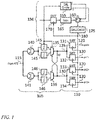
- a hybrid half/quarter-rate decision feedback equalizer includes a first stage 105, consisting of current mode logic (CML) circuits, and a second stage 110, consisting of complementary metal oxide semiconductor (CMOS) circuits.
- the hybrid half/quarter-rate DFE has an analog input 115 for receiving a high-speed serial data signal, and four digital outputs 120, at which the serial data are produced, parallelized by a factor of 4 (and transmitted, at each of the four digital outputs 120, at one quarter the rate of the received serial data).
- the CML circuits may operate in a first clock domain, having a first, half-rate, clock (i.e., a clock that has one period for every two bits of the received serial data signal) and the CMOS circuits may operate in a second clock domain, having a second, quarter-rate, clock, i.e., a clock with a frequency that is one half of the frequency of the first clock.
- the first clock may be generated from the received serial data signal by a clock recovery circuit.
- Each CML circuit may operate with differential digital signals assuming, at any time, one of two discrete differential voltage values.
- Each of the conductors carrying a differential CML signal may have a voltage swing (in changing between the two states) of, for example, 0.4 V (which may be significantly less than the difference between Vdd and ground); accordingly, the differential swing may be 0.8 V.
- Each CMOS circuit may similarly operate with digital signals assuming, at any time, one of two discrete voltage values, the two values being near ground and near Vdd, respectively.
- the first stage 105 includes an analog input that is (e.g., that is connected to) the analog input 115 of the two-stage quarter-rate decision feedback equalizer, a first digital output 125, and a second digital output 130.
- the first stage 105 includes (i) a first path including a first adder 140, a first pair of clocked comparators (or “samplers” or “slicers") 145, and a first multiplexer 135 feeding the first digital output 125 of the first stage 105, and (ii) a second path including a second adder 141, a second pair of clocked comparators 146, and a second multiplexer 136 feeding the second digital output 130 of the first stage 105.
- Each of the multiplexers 135, 136 may be a latching multiplexer (or "MUX-latch").
- Serial data bits from the received serial data stream are produced alternately at the first digital output 125, and at the second digital output 130; each output is used by a multiplexer 135, 136 in the circuit feeding the other output to select between two predictively corrected data values, each corrected based on a respective one of the two possible values of the data bit received immediately previously.
- the first digital output 125 may be configured to generate a digital data value with every cycle of the first clock during a portion of a time interval when the first clock is low.
- the second digital output 130 may be configured to generate a digital data value with every cycle of the first clock during a portion of a time interval when the first clock is high.
- the second stage 110 includes four flip flops (e.g., strong arm flip flops, "SAFF") 131, 132, 133, 134, each having an output that is (e.g., that is connected to) a respective one of the four digital outputs 120, a data input, and a clock input.
- SAFF strong arm flip flops
- the clock signals fed to the clock inputs of the first two flip flops 131, 132 have triggering edges (e.g., rising edges) timed so that the flip flops capture alternating bits from the first digital output 125, as discussed in further detail below, and the clock signals fed to the clock inputs of the third and fourth flip flops 133, 134 have triggering edges timed so that the flip flops capture alternating bits from the second digital output 130.
- Each flip flop 131, 132, 133, 134 may also serve as a CML-to-CMOS converter for data.
- a clock synchronization circuit 150 may be employed to synchronize the second clock (the quarter-rate clock) to the first clock (the half-rate clock).
- the clock synchronization circuit 150 includes a CML divider 155, a phase interpolator 160, a control logic circuit 165, a replica flip flop 170 (which may be a copy of the strong arm flip flops 131, 132, 133, 134, all of which may be nominally identical), and a CML to CMOS conversion circuit 175.
- the output 180 of the CML to CMOS conversion circuit 175 includes four phases of the second clock, which may, for example be transmitted on two pairs of conductors (i.e., four conductors), each of which may carry a differential signal (i.e., a signal and its complement). Of these four conductors a first pair of conductors may carry a first phase of the second clock and its complement, and the second pair of conductors may carry a third phase of the second clock and its complement. A second phase of the second clock may be formed by inverting the first phase (i.e., by interchanging the conductors) and a fourth phase of the second clock may be formed by inverting the third phase (i.e., by interchanging the conductors). The first, second, third and fourth phases may be fed to the clock inputs of the first flip flop 131, the second flip flop 132, the third flip flop 133, and the fourth flip flop 134, respectively.
- the CML divider 155 generates two signals, an in-phase signal and a quadrature phase signal, each at one half of the frequency of the first clock.
- the replica flip flop 170 receives at its data input the first clock, and at its clock input the first phase of the second clock.
- the control logic circuit 165 adjusts the phase of the phase interpolator 160 based on whether the output of the replica flip flop 170 consists primarily of zeros or ones, so that edges of the first clock are aligned with rising edges of the second clock (e.g., so that falling edges of the first clock are aligned with rising edges of the first phase of the second clock (see FIG. 3 )).
- the control logic circuit 165 may for example include a counter that counts up when a one is received and that counts down when a zero is received (or vice versa), and the value of the count may periodically be sent to the phase interpolator 160 as a phase command.
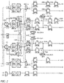
- FIG. 2 shows the first stage and the second stage of the hybrid half/quarter-rate DFE, as well as additional circuits used to generate crossing clocks and crossing data (x ⁇ 0>, x ⁇ 1>, x ⁇ 2>, x ⁇ 3>) which may be used by the clock recovery circuit, and to control the phase of the first clock at the data slicers and crossing slicers of the first stage.
- Each of the circuits for producing the crossing data may include a portion within the first stage, e.g., up to and including the multiplexers (labeled "MuxL") (and these portions may be constructed of CML circuits), and a portion within the second stage (beginning with the strong arm flip flops receiving the signals from the multiplexers) (and these portions may be constructed of CMOS circuits).
- MuxL multiplexers
- FIG. 2 shows a partial timing diagram for the circuit of FIGs. 1 and 2 .
- the timing waveform for the first digital output 125 is shown as the fourth waveform of FIG. 3 , labelled "MuxL-out”.
- the input data stream containing data bits "A”, “B”, “C”, etc., is the first waveform shown; the sixth and seventh waveforms show the first and fifth bits (“A” and “E") being transmitted at the output of the first flip flop 131, and the third and seventh bits (“C” and “G”) being transmitted at the output of the second flip flop 132.
- the first phase of the second clock (the quarter-rate clock) is the fifth waveform ("dclk_0p") (and the second phase is its complement).
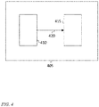
- a display 405 contains a timing controller 410 configured to send high-speed digital data to a driver integrated circuit (driver IC) 415, over a serial data link 420.
- the driver integrated circuit 415 includes a serial data receiver, at the receiving end of the serial data link 420, constructed according to an embodiment of the present disclosure.
- a phase of a clock signal is a version of the clock signal having some phase offset with respect to a first phase of the clock signal.
- a differential clock signal is referred to herein as a two-phase clock, if in some circuits the clock is connected to have an effect on a first edge (e.g., a rising edge of the clock signal) and in some circuits the clock is connected to have an effect on a second edge (e.g., a rising edge of the complementary clock signal).
- first, second, third, etc. may be used herein to describe various elements, components, regions, layers and/or sections, these elements, components, regions, layers and/or sections should not be limited by these terms. These terms are only used to distinguish one element, component, region, layer or section from another element, component, region, layer or section. Thus, a first element, component, region, layer or section discussed herein could be termed a second element, component, region, layer or section, without departing from the scope of the inventive concept.
- spatially relative terms such as “beneath”, “below”, “lower”, “under”, “above”, “upper” and the like, may be used herein for ease of description to describe one element or feature's relationship to another element(s) or feature(s) as illustrated in the figures. It will be understood that such spatially relative terms are intended to encompass different orientations of the device in use or in operation, in addition to the orientation depicted in the figures. For example, if the device in the figures is turned over, elements described as “below” or “beneath” or “under” other elements or features would then be oriented “above” the other elements or features. Thus, the example terms “below” and “under” can encompass both an orientation of above and below.
- the device may be otherwise oriented (e.g., rotated 90 degrees or at other orientations) and the spatially relative descriptors used herein should be interpreted accordingly.
- a layer when referred to as being "between" two layers, it can be the only layer between the two layers, or one or more intervening layers may also be present.
- any numerical range recited herein is intended to include all sub-ranges of the same numerical precision subsumed within the recited range.
- a range of "1.0 to 10.0" is intended to include all subranges between (and including) the recited minimum value of 1.0 and the recited maximum value of 10.0, that is, having a minimum value equal to or greater than 1.0 and a maximum value equal to or less than 10.0, such as, for example, 2.4 to 7.6.
- Any maximum numerical limitation recited herein is intended to include all lower numerical limitations subsumed therein and any minimum numerical limitation recited in this specification is intended to include all higher numerical limitations subsumed therein.
Landscapes
- Engineering & Computer Science (AREA)
- Signal Processing (AREA)
- Computer Networks & Wireless Communication (AREA)
- Power Engineering (AREA)
- Computer Hardware Design (AREA)
- Physics & Mathematics (AREA)
- Theoretical Computer Science (AREA)
- General Engineering & Computer Science (AREA)
- Computing Systems (AREA)
- Mathematical Physics (AREA)
- General Physics & Mathematics (AREA)
- Cable Transmission Systems, Equalization Of Radio And Reduction Of Echo (AREA)
- Dc Digital Transmission (AREA)
Abstract
Description
- One or more aspects of embodiments according to the present invention relate to serial data receivers, and more particularly to a decision feedback equalizer for a serial data receiver, and a display comprising such a decision feedback equalizer.
- In an integrated circuit, a serial data receiver may be configured to operate at high speed, to achieve high data rate data transfers with other integrated circuits. In some embodiments the data rate and the corresponding clock rate may be sufficiently high that complementary metal oxide semiconductor (CMOS) circuits also within the integrated circuit may be incapable of operating at the same clock rate, or would exhibit unacceptably high power consumption were they operating at such a clock rate.
- In such cases, a half-rate or quarter-rate decision feedback equalizer may be employed to convert the received serial data stream into two or four parallel data streams each at one half or one quarter, respectively, of the received data. Such a half-rate or quarter-rate decision feedback equalizer may be implemented in current mode logic, which, however, may exhibit relatively high power consumption.
- Thus, there is a need for a low-power circuit for reducing the data rate of serial data.
- According to an embodiment of the present disclosure, there is provided a two-stage decision feedback equalizer for receiving serial data, at an analog input, at a first data rate, the two-stage decision feedback equalizer comprising: a first stage, comprising a half-rate predictive decision feedback equalizer having: an analog input connected to the analog input of the two-stage decision feedback equalizer, a first digital output, and a second digital output; and a second stage, comprising: a first flip flop having a data input connected to the first digital output, a second flip flop having a data input connected to the first digital output, a third flip flop having a data input connected to the second digital output, and a fourth flip flop having a data input connected to the second digital output, the first stage being in a first clock domain configured to operate with a first clock at a frequency equal to one half of the first data rate, and the second stage being in a second clock domain configured to operate with a second clock at a frequency equal to one quarter of the first data rate.
- In some embodiments, the first stage comprises current mode logic circuits.
- In some embodiments, the second stage comprises complementary metal oxide semiconductor circuits.
- In some embodiments, the first stage comprises: a first path having an input connected to the analog input, and a second path having an input connected to the analog input, the first path being configured to generate, at the first digital output, a digital data value with every cycle of the first clock, during a portion of a time interval when the first clock is low; and the second path being configured to generate, at the second digital output, a digital data value with every cycle of the first clock, during a portion of a time interval when the first clock is high.
- In some embodiments, the two-stage decision feedback equalizer further comprises a phase control circuit configured to align transitions of a first phase of the second clock with transitions of a first phase of the first clock.
- In some embodiments, the phase control circuit comprises a fifth flip flop having: a data input connected to the first phase of the first clock, a clock input connected to the first phase of the second clock, and an output.
- In some embodiments, the phase control circuit further comprises: a phase interpolator, configured: to receive: two phases of the second clock, the two phases differing by more than 0 degrees and less than 180 degrees, and a control signal; and to form, as output, a signal having a phase corresponding to the control signal.
- In some embodiments, the two phases differ by around 90 degrees.
- In some embodiments, the two-stage decision feedback equalizer further comprises a logic circuit having: an input connected to the output of the fifth flip flop, and an output connected to the phase interpolator, the logic circuit being configured to generate the control signal for the phase interpolator.
- In some embodiments, the logic circuit comprises an up-down counter, configured: to increment a count value when the output of the fifth flip flop is high and to decrement the count value when the output of the fifth flip flop is low.
- In some embodiments, the logic circuit comprises an up-down counter, configured: to increment a count value when the output of the fifth flip flop has a first state and to decrement the count value when the output of the fifth flip flop has a second state. The first state may be a high state. The second state may be a low state.
- In some embodiments, the first flip flop has a clock input configured to receive a first phase of the second clock, the first phase of the second clock having a rising edge aligned with every other falling edge of the first clock.
- In some embodiments, the second flip flop has a clock input configured to receive a second phase of the second clock, the second phase of the second clock having a rising edge aligned with every falling edge of the first phase of the second clock.
- In some embodiments, the third flip flop has a clock input configured to receive a third phase of the second clock, the third phase of the second clock having a rising edge following each rising edge of the first phase of the second clock by one quarter cycle of the second clock.
- In some embodiments, the fourth flip flop has a clock input configured to receive a fourth phase of the second clock, the fourth phase of the second clock having a rising edge aligned with every falling edge of the third phase of the second clock.
- According to an embodiment of the present disclosure, there is provided a two-stage decision feedback equalizer for receiving serial data, at an analog input, at a first data rate, the two-stage decision feedback equalizer comprising: a first stage, connected to the analog input, the first stage comprising a half-rate predictive decision feedback equalizer comprising current mode logic circuits; and a second stage, connected to the first stage, the second stage comprising complementary metal oxide semiconductor circuits.
- In some embodiments: the half-rate predictive decision feedback equalizer of the first stage has: an analog input connected to the analog input of the two-stage decision feedback equalizer, a first digital output, and a second digital output; and the second stage comprises: a first flip flop having a data input connected to the first digital output, a second flip flop having a data input connected to the first digital output, a third flip flop having a data input connected to the second digital output, and a fourth flip flop having a data input connected to the second digital output, the first stage being in a first clock domain configured to operate with a first clock at a frequency equal to one half of the first data rate, and the second stage being in a second clock domain configured to operate with a second clock at a frequency equal to one quarter of the first data rate.
- In some embodiments, the first stage comprises: a first path having an input connected to the analog input, and a second path having an input connected to the analog input, the first path being configured to generate, at the first digital output, a digital data value with every cycle of the first clock, during a portion of a time interval when the first clock is low; and the second path being configured to generate, at the second digital output, a digital data value with every cycle of the first clock, during a portion of a time interval when the first clock is high.
- In some embodiments, the two-stage decision feedback equalizer further comprises a phase control circuit configured to align transitions of a first phase of the second clock with transitions of a first phase of the first clock.
- In some embodiments, the phase control circuit comprises a fifth flip flop having: a data input connected to the first phase of the first clock, a clock input connected to the first phase of the second clock, and an output.
- In some embodiments , the phase control circuit further comprises: a phase interpolator, configured: to receive: two phases of the second clock, the two phases differing by more than 0 degrees and less than 180 degrees, and a control signal; and to form, as output, a signal having a phase corresponding to the control signal.
- In some embodiments, the two phases differ by around 90 degrees.
- According to an embodiment of the present disclosure, there is provided a display, comprising: a timing controller having a serial data output; and a driver integrated circuit having an analog input for receiving serial data, at a first data rate, the driver integrated circuit comprising a two-stage decision feedback equalizer for receiving the serial data, the two-stage decision feedback equalizer having an analog input connected to the analog input of the driver integrated circuit, the two-stage decision feedback equalizer comprising: a first stage, connected to the analog input, the first stage comprising a half-rate predictive decision feedback equalizer comprising current mode logic circuits; and a second stage, connected to the first stage, the second stage comprising complementary metal oxide semiconductor circuits.
- According to an embodiment of the present disclosure, there is provided a display, comprising: a timing controller having a serial data output; and a driver integrated circuit having an analog input for receiving serial data, at a first data rate. The driver integrated circuit comprises a two-stage decision feedback equalizer for receiving the serial data, the two-stage decision feedback equalizer has an analog input connected to the analog input of the driver integrated circuit. The two-stage decision feedback equalizer comprises a two-stage decision feedback equalizer according to another embodiment of the present disclosure.
- It will be appreciated that features described in the context of, or in combination with, one embodiment of the present disclosure may be used in combination with other embodiments described herein.
- At least some of the above features that accord with the invention and other features according to the invention are set out in the claims.
- These and other features and advantages of the present disclosure will be appreciated and understood with reference to the specification, claims, and appended drawings wherein:
-
FIG. 1 is a schematic diagram of a two-stage decision feedback equalizer, according to an embodiment of the present disclosure; -
FIG. 2 is a schematic diagram of a two-stage decision feedback equalizer, according to an embodiment of the present disclosure; -
FIG. 3 is a timing diagram of a two-stage decision feedback equalizer, according to an embodiment of the present disclosure; and -
FIG. 4 is a block diagram of a display, according to an embodiment of the present disclosure. - The detailed description set forth below in connection with the appended drawings is intended as a description of embodiments of a hybrid half/quarter-rate DFE provided in accordance with the present disclosure and is not intended to represent the only forms in which the present disclosure may be constructed or utilized. The description sets forth the features of the present disclosure in connection with the illustrated embodiments. It is to be understood, however, that the same or equivalent functions and structures may be accomplished by different embodiments that are also intended to be encompassed within the scope of the disclosure. As denoted elsewhere herein, like element numbers are intended to indicate like elements or features.
- Referring to
FIG. 1 , in some embodiments a hybrid half/quarter-rate decision feedback equalizer (DFE) includes afirst stage 105, consisting of current mode logic (CML) circuits, and asecond stage 110, consisting of complementary metal oxide semiconductor (CMOS) circuits. The hybrid half/quarter-rate DFE has ananalog input 115 for receiving a high-speed serial data signal, and fourdigital outputs 120, at which the serial data are produced, parallelized by a factor of 4 (and transmitted, at each of the fourdigital outputs 120, at one quarter the rate of the received serial data). The CML circuits may operate in a first clock domain, having a first, half-rate, clock (i.e., a clock that has one period for every two bits of the received serial data signal) and the CMOS circuits may operate in a second clock domain, having a second, quarter-rate, clock, i.e., a clock with a frequency that is one half of the frequency of the first clock. The first clock may be generated from the received serial data signal by a clock recovery circuit. Each CML circuit may operate with differential digital signals assuming, at any time, one of two discrete differential voltage values. Each of the conductors carrying a differential CML signal may have a voltage swing (in changing between the two states) of, for example, 0.4 V (which may be significantly less than the difference between Vdd and ground); accordingly, the differential swing may be 0.8 V. Each CMOS circuit may similarly operate with digital signals assuming, at any time, one of two discrete voltage values, the two values being near ground and near Vdd, respectively. - The
first stage 105 includes an analog input that is (e.g., that is connected to) theanalog input 115 of the two-stage quarter-rate decision feedback equalizer, a firstdigital output 125, and a seconddigital output 130. Thefirst stage 105 includes (i) a first path including afirst adder 140, a first pair of clocked comparators (or "samplers" or "slicers") 145, and afirst multiplexer 135 feeding the firstdigital output 125 of thefirst stage 105, and (ii) a second path including asecond adder 141, a second pair of clockedcomparators 146, and asecond multiplexer 136 feeding the seconddigital output 130 of thefirst stage 105. Each of themultiplexers - Serial data bits from the received serial data stream are produced alternately at the first
digital output 125, and at the seconddigital output 130; each output is used by amultiplexer digital output 125 may be configured to generate a digital data value with every cycle of the first clock during a portion of a time interval when the first clock is low. The seconddigital output 130 may be configured to generate a digital data value with every cycle of the first clock during a portion of a time interval when the first clock is high. - The
second stage 110 includes four flip flops (e.g., strong arm flip flops, "SAFF") 131, 132, 133, 134, each having an output that is (e.g., that is connected to) a respective one of the fourdigital outputs 120, a data input, and a clock input. The data inputs of the first twoflip flops digital output 125, and the data inputs of third andfourth flip flops digital output 130. The clock signals fed to the clock inputs of the first twoflip flops digital output 125, as discussed in further detail below, and the clock signals fed to the clock inputs of the third andfourth flip flops digital output 130. Eachflip flop - In some embodiments a
clock synchronization circuit 150 may be employed to synchronize the second clock (the quarter-rate clock) to the first clock (the half-rate clock). Theclock synchronization circuit 150 includes aCML divider 155, aphase interpolator 160, acontrol logic circuit 165, a replica flip flop 170 (which may be a copy of the strongarm flip flops CMOS conversion circuit 175. Theoutput 180 of the CML to CMOSconversion circuit 175 includes four phases of the second clock, which may, for example be transmitted on two pairs of conductors (i.e., four conductors), each of which may carry a differential signal (i.e., a signal and its complement). Of these four conductors a first pair of conductors may carry a first phase of the second clock and its complement, and the second pair of conductors may carry a third phase of the second clock and its complement. A second phase of the second clock may be formed by inverting the first phase (i.e., by interchanging the conductors) and a fourth phase of the second clock may be formed by inverting the third phase (i.e., by interchanging the conductors). The first, second, third and fourth phases may be fed to the clock inputs of thefirst flip flop 131, thesecond flip flop 132, thethird flip flop 133, and thefourth flip flop 134, respectively. - The
CML divider 155 generates two signals, an in-phase signal and a quadrature phase signal, each at one half of the frequency of the first clock. Thereplica flip flop 170 receives at its data input the first clock, and at its clock input the first phase of the second clock. Thecontrol logic circuit 165 adjusts the phase of thephase interpolator 160 based on whether the output of thereplica flip flop 170 consists primarily of zeros or ones, so that edges of the first clock are aligned with rising edges of the second clock (e.g., so that falling edges of the first clock are aligned with rising edges of the first phase of the second clock (seeFIG. 3 )). Thecontrol logic circuit 165 may for example include a counter that counts up when a one is received and that counts down when a zero is received (or vice versa), and the value of the count may periodically be sent to thephase interpolator 160 as a phase command. -
FIG. 2 shows the first stage and the second stage of the hybrid half/quarter-rate DFE, as well as additional circuits used to generate crossing clocks and crossing data (x<0>, x<1>, x<2>, x<3>) which may be used by the clock recovery circuit, and to control the phase of the first clock at the data slicers and crossing slicers of the first stage. Each of the circuits for producing the crossing data may include a portion within the first stage, e.g., up to and including the multiplexers (labeled "MuxL") (and these portions may be constructed of CML circuits), and a portion within the second stage (beginning with the strong arm flip flops receiving the signals from the multiplexers) (and these portions may be constructed of CMOS circuits). - Also shown in
FIG. 2 are pass transistor logic (PTL) latches 210 that are used to align the phases of the four digital outputs (d<0>, d<1>, d<2>, d<3>).FIG. 3 shows a partial timing diagram for the circuit ofFIGs. 1 and2 . The timing waveform for the firstdigital output 125 is shown as the fourth waveform ofFIG. 3 , labelled "MuxL-out". The input data stream containing data bits "A", "B", "C", etc., is the first waveform shown; the sixth and seventh waveforms show the first and fifth bits ("A" and "E") being transmitted at the output of thefirst flip flop 131, and the third and seventh bits ("C" and "G") being transmitted at the output of thesecond flip flop 132. The first phase of the second clock (the quarter-rate clock) is the fifth waveform ("dclk_0p") (and the second phase is its complement). - Referring to
FIG. 4 , in one embodiment adisplay 405 contains atiming controller 410 configured to send high-speed digital data to a driver integrated circuit (driver IC) 415, over aserial data link 420. The driver integratedcircuit 415 includes a serial data receiver, at the receiving end of theserial data link 420, constructed according to an embodiment of the present disclosure. - As used herein, a "phase" of a clock signal is a version of the clock signal having some phase offset with respect to a first phase of the clock signal. As such, a differential clock signal is referred to herein as a two-phase clock, if in some circuits the clock is connected to have an effect on a first edge (e.g., a rising edge of the clock signal) and in some circuits the clock is connected to have an effect on a second edge (e.g., a rising edge of the complementary clock signal).
- It will be understood that, although the terms "first", "second", "third", etc., may be used herein to describe various elements, components, regions, layers and/or sections, these elements, components, regions, layers and/or sections should not be limited by these terms. These terms are only used to distinguish one element, component, region, layer or section from another element, component, region, layer or section. Thus, a first element, component, region, layer or section discussed herein could be termed a second element, component, region, layer or section, without departing from the scope of the inventive concept.
- Spatially relative terms, such as "beneath", "below", "lower", "under", "above", "upper" and the like, may be used herein for ease of description to describe one element or feature's relationship to another element(s) or feature(s) as illustrated in the figures. It will be understood that such spatially relative terms are intended to encompass different orientations of the device in use or in operation, in addition to the orientation depicted in the figures. For example, if the device in the figures is turned over, elements described as "below" or "beneath" or "under" other elements or features would then be oriented "above" the other elements or features. Thus, the example terms "below" and "under" can encompass both an orientation of above and below. The device may be otherwise oriented (e.g., rotated 90 degrees or at other orientations) and the spatially relative descriptors used herein should be interpreted accordingly. In addition, it will also be understood that when a layer is referred to as being "between" two layers, it can be the only layer between the two layers, or one or more intervening layers may also be present.
- The terminology used herein is for the purpose of describing particular embodiments only and is not intended to be limiting of the inventive concept. As used herein, the terms "substantially," "about," and similar terms are used as terms of approximation and not as terms of degree, and are intended to account for the inherent deviations in measured or calculated values that would be recognized by those of ordinary skill in the art.
- As used herein, the singular forms "a" and "an" are intended to include the plural forms as well, unless the context clearly indicates otherwise. It will be further understood that the terms "comprises" and/or "comprising", when used in this specification, specify the presence of stated features, integers, steps, operations, elements, and/or components, but do not preclude the presence or addition of one or more other features, integers, steps, operations, elements, components, and/or groups thereof. As used herein, the term "and/or" includes any and all combinations of one or more of the associated listed items. Expressions such as "at least one of," when preceding a list of elements, modify the entire list of elements and do not modify the individual elements of the list. Further, the use of "may" when describing embodiments of the inventive concept refers to "one or more embodiments of the present invention". As used herein, the terms "use," "using," and "used" may be considered synonymous with the terms "utilize," "utilizing," and "utilized," respectively.
- It will be understood that when an element or layer is referred to as being "on", "connected to", "coupled to", or "adjacent to" another element or layer, it may be directly on, connected to, coupled to, or adjacent to the other element or layer, or one or more intervening elements or layers may be present. In contrast, when an element or layer is referred to as being "directly on", "directly connected to", "directly coupled to", or "immediately adjacent to" another element or layer, there are no intervening elements or layers present.
- Any numerical range recited herein is intended to include all sub-ranges of the same numerical precision subsumed within the recited range. For example, a range of "1.0 to 10.0" is intended to include all subranges between (and including) the recited minimum value of 1.0 and the recited maximum value of 10.0, that is, having a minimum value equal to or greater than 1.0 and a maximum value equal to or less than 10.0, such as, for example, 2.4 to 7.6. Any maximum numerical limitation recited herein is intended to include all lower numerical limitations subsumed therein and any minimum numerical limitation recited in this specification is intended to include all higher numerical limitations subsumed therein.
- Although embodiments of a hybrid half/quarter-rate DFE have been specifically described and illustrated herein, many modifications and variations will be apparent to those skilled in the art. Accordingly, it is to be understood that a hybrid half/quarter-rate DFE constructed according to principles of this invention may be embodied other than as specifically described herein. The invention is also defined in the following claims, and equivalents thereof.
Claims (20)
- A two-stage decision feedback equalizer for receiving serial data, at an analog input, at a first data rate,
the two-stage decision feedback equalizer comprising:a first stage, comprising a half-rate predictive decision feedback equalizer having:an analog input connected to the analog input of the two-stage decision feedback equalizer,a first digital output, anda second digital output; anda second stage, comprising:the first stage being in a first clock domain configured to operate with a first clock at a frequency equal to one half of the first data rate, anda first flip flop having a data input connected to the first digital output,a second flip flop having a data input connected to the first digital output,a third flip flop having a data input connected to the second digital output, anda fourth flip flop having a data input connected to the second digital output,
the second stage being in a second clock domain configured to operate with a second clock at a frequency equal to one quarter of the first data rate. - A two-stage decision feedback equalizer according to claim 1, wherein the first stage comprises current mode logic circuits.
- A two-stage decision feedback equalizer according to claim 1 or claim 2, wherein the second stage comprises complementary metal oxide semiconductor circuits.
- A two-stage decision feedback equalizer according to any preceding claim, wherein the first stage comprises:a first path having an input connected to the analog input, anda second path having an input connected to the analog input,the first path being configured to generate, at the first digital output, a digital data value with every cycle of the first clock, during a portion of a time interval when the first clock is low; andthe second path being configured to generate, at the second digital output, a digital data value with every cycle of the first clock, during a portion of a time interval when the first clock is high.
- A two-stage decision feedback equalizer according to any preceding claim, further comprising a phase control circuit configured to align transitions of a first phase of the second clock with transitions of a first phase of the first clock.
- A two-stage decision feedback equalizer according to claim 5, wherein the phase control circuit comprises a fifth flip flop having:a data input connected to the first phase of the first clock,a clock input connected to the first phase of the second clock, andan output.
- A two-stage decision feedback equalizer according to claim 6, wherein the phase control circuit further comprises:
a phase interpolator, configured:to receive:two phases of the second clock, the two phases differing by more than 0 degrees and less than 180 degrees, anda control signal; andto form, as output, a signal having a phase corresponding to the control signal. - A two-stage decision feedback equalizer according to claim 7, further comprising a logic circuit having:an input connected to the output of the fifth flip flop, andan output connected to the phase interpolator, the logic circuit being configured to generate the control signal for the phase interpolator.
- A two-stage decision feedback equalizer according to claim 8, wherein the logic circuit comprises an up-down counter, configured:to increment a count value when the output of the fifth flip flop has a first state andto decrement the count value when the output of the fifth flip flop has a second state.
- A two-stage decision feedback equalizer according to any preceding claim, wherein the first flip flop has a clock input configured to receive a first phase of the second clock, the first phase of the second clock having a rising edge aligned with every other falling edge of the first clock.
- A two-stage decision feedback equalizer according to claim 10, wherein the second flip flop has a clock input configured to receive a second phase of the second clock, the second phase of the second clock having a rising edge aligned with every falling edge of the first phase of the second clock.
- A two-stage decision feedback equalizer according to claim 11, wherein the third flip flop has a clock input configured to receive a third phase of the second clock, the third phase of the second clock having a rising edge following each rising edge of the first phase of the second clock by one quarter cycle of the second clock.
- A two-stage decision feedback equalizer according to claim 12, wherein the fourth flip flop has a clock input configured to receive a fourth phase of the second clock, the fourth phase of the second clock having a rising edge aligned with every falling edge of the third phase of the second clock.
- A two-stage decision feedback equalizer for receiving serial data, at an analog input, at a first data rate,
the two-stage decision feedback equalizer comprising:a first stage, connected to the analog input, the first stage comprising a half-rate predictive decision feedback equalizer comprising current mode logic circuits; anda second stage, connected to the first stage, the second stage comprising complementary metal oxide semiconductor circuits. - A two-stage decision feedback equalizer according to claim 14, wherein:the half-rate predictive decision feedback equalizer of the first stage has:an analog input connected to the analog input of the two-stage decision feedback equalizer,a first digital output, anda second digital output; andthe second stage comprises:a first flip flop having a data input connected to the first digital output,a second flip flop having a data input connected to the first digital output,a third flip flop having a data input connected to the second digital output, anda fourth flip flop having a data input connected to the second digital output,the first stage being in a first clock domain configured to operate with a first clock at a frequency equal to one half of the first data rate, andthe second stage being in a second clock domain configured to operate with a second clock at a frequency equal to one quarter of the first data rate.
- A two-stage decision feedback equalizer according to claim 15, wherein the first stage comprises:a first path having an input connected to the analog input, anda second path having an input connected to the analog input,the first path being configured to generate, at the first digital output, a digital data value with every cycle of the first clock, during a portion of a time interval when the first clock is low; andthe second path being configured to generate, at the second digital output, a digital data value with every cycle of the first clock, during a portion of a time interval when the first clock is high.
- A two-stage decision feedback equalizer according to claim 15 or claim 16, further comprising a phase control circuit configured to align transitions of a first phase of the second clock with transitions of a first phase of the first clock.
- A two-stage decision feedback equalizer according to claim 17, wherein the phase control circuit comprises a fifth flip flop having:a data input connected to the first phase of the first clock,a clock input connected to the first phase of the second clock, andan output.
- A two-stage decision feedback equalizer according to claim 18, wherein the phase control circuit further comprises:
a phase interpolator, configured:
to receive:two phases of the second clock, the two phases differing by more than 0 degrees and less than 180 degrees, anda control signal; andto form, as output, a signal having a phase corresponding to the control signal. - A display, comprising:a timing controller having a serial data output; anda driver integrated circuit having an analog input for receiving serial data, at a first data rate,the driver integrated circuit comprising a two-stage decision feedback equalizer for receiving the serial data, the two-stage decision feedback equalizer comprising a two-stage decision feedback equalizer according to any preceding claim having an analog input connected to the analog input of the driver integrated circuit.
Applications Claiming Priority (2)
| Application Number | Priority Date | Filing Date | Title |
|---|---|---|---|
| US201862638739P | 2018-03-05 | 2018-03-05 | |
| US16/058,896 US10476707B2 (en) | 2018-03-05 | 2018-08-08 | Hybrid half/quarter-rate DFE |
Publications (2)
| Publication Number | Publication Date |
|---|---|
| EP3537610A2 true EP3537610A2 (en) | 2019-09-11 |
| EP3537610A3 EP3537610A3 (en) | 2019-12-04 |
Family
ID=65717817
Family Applications (1)
| Application Number | Title | Priority Date | Filing Date |
|---|---|---|---|
| EP19160874.4A Ceased EP3537610A3 (en) | 2018-03-05 | 2019-03-05 | Hybrid half/quarter-rate decision feedback equalizer and display including hybrid half/quarter-rate decision feedback equalizer |
Country Status (6)
| Country | Link |
|---|---|
| US (1) | US10476707B2 (en) |
| EP (1) | EP3537610A3 (en) |
| JP (1) | JP7388818B2 (en) |
| KR (1) | KR102610853B1 (en) |
| CN (1) | CN110232886B (en) |
| TW (1) | TWI799526B (en) |
Families Citing this family (8)
| Publication number | Priority date | Publication date | Assignee | Title |
|---|---|---|---|---|
| US11302267B2 (en) | 2020-05-20 | 2022-04-12 | Novatek Microelectronics Corp. | LED display panel having a driver device for equalizing data lines and operation method thereof |
| US11502884B2 (en) * | 2020-07-09 | 2022-11-15 | Texas Instruments Incorporated | Phase prediction demodulator circuits and related method |
| CN112422461B (en) | 2020-11-05 | 2022-04-19 | 硅谷数模(苏州)半导体有限公司 | Decision feedback equalizer and data acquisition and correction method |
| US11477057B1 (en) * | 2021-06-22 | 2022-10-18 | Samsung Electronics Co., Ltd. | Quarter rate speculative decision feedback equalizer (DFE) and method for operating thereof |
| CN115102812B (en) * | 2022-02-18 | 2025-10-31 | 中国科学院微电子研究所 | High-speed digital feedback equalization device and method |
| US11677593B1 (en) * | 2022-05-24 | 2023-06-13 | Cadence Design Systems, Inc. | Sampler with built-in DFE and offset cancellation |
| US11770274B1 (en) * | 2022-05-24 | 2023-09-26 | Apple Inc. | Receiver with half-rate sampler circuits |
| CN118611791B (en) * | 2024-08-02 | 2024-10-29 | 联芸科技(杭州)股份有限公司 | A calibration circuit, a chip and a parameter calibration method |
Family Cites Families (20)
| Publication number | Priority date | Publication date | Assignee | Title |
|---|---|---|---|---|
| JPH06311156A (en) * | 1993-04-22 | 1994-11-04 | Fujitsu Ltd | Frame synchronizing circuit |
| JP2002057572A (en) | 2000-08-08 | 2002-02-22 | Mitsubishi Electric Corp | Phase locked loop |
| US7697603B1 (en) | 2004-10-18 | 2010-04-13 | Altera Corporation | Methods and apparatus for equalization in high-speed backplane data communication |
| JP2007312321A (en) | 2006-05-22 | 2007-11-29 | Sharp Corp | Semiconductor integrated circuit for serial / parallel conversion |
| US7715474B2 (en) | 2007-02-07 | 2010-05-11 | International Business Machines Corporation | Decision feedback equalizer (DFE) architecture |
| US7936812B2 (en) | 2007-07-02 | 2011-05-03 | Micron Technology, Inc. | Fractional-rate decision feedback equalization useful in a data transmission system |
| US8126045B2 (en) * | 2008-08-29 | 2012-02-28 | International Business Machines Corporation | System and method for latency reduction in speculative decision feedback equalizers |
| US8477833B2 (en) | 2009-02-06 | 2013-07-02 | International Business Machines Corporation | Circuits and methods for DFE with reduced area and power consumption |
| US8401065B2 (en) | 2011-02-14 | 2013-03-19 | Fujitsu Limited | Clock recovery circuit for receiver using decision feedback equalizer |
| CN102801667B (en) * | 2011-05-26 | 2015-04-15 | 北京大学 | Current integrating decision feedback equalizer used in high-speed serial interface |
| JP5952072B2 (en) * | 2012-04-26 | 2016-07-13 | ルネサスエレクトロニクス株式会社 | Encoding device, decoding device, and transmission system |
| US9106461B2 (en) | 2012-07-20 | 2015-08-11 | Fujitsu Limited | Quarter-rate speculative decision feedback equalizer |
| US9319248B2 (en) * | 2012-12-21 | 2016-04-19 | Nvidia Corporation | Decision feedback equalizer using current mode processing with CMOS compatible output level |
| US9674008B2 (en) | 2013-10-31 | 2017-06-06 | Samsung Display Co., Ltd. | Body-biased slicer design for predictive decision feedback equalizers |
| JP6334183B2 (en) | 2014-01-31 | 2018-05-30 | 株式会社日立製作所 | Optical transmission circuit |
| US9531570B2 (en) * | 2014-05-27 | 2016-12-27 | Samsung Display Co., Ltd | CML quarter-rate predictive feedback equalizer architecture |
| JP6428279B2 (en) | 2015-01-13 | 2018-11-28 | 株式会社ソシオネクスト | Reception circuit, transmission / reception circuit, and integrated circuit |
| CN104660227B (en) * | 2015-03-07 | 2017-04-19 | 浙江大学 | Adaptive continuous time linear equalizer suitable for multi-level pulse amplitude modulation |
| US9680436B1 (en) * | 2016-03-28 | 2017-06-13 | Samsung Display Co., Ltd. | System and method for setting analog front end DC gain |
| US10200025B2 (en) * | 2016-12-27 | 2019-02-05 | Intel Corporation | Pulse-amplitude modulated hybrid comparator circuit |
-
2018
- 2018-08-08 US US16/058,896 patent/US10476707B2/en active Active
-
2019
- 2019-02-18 KR KR1020190018525A patent/KR102610853B1/en active Active
- 2019-03-04 JP JP2019038613A patent/JP7388818B2/en active Active
- 2019-03-05 TW TW108107288A patent/TWI799526B/en active
- 2019-03-05 CN CN201910163968.9A patent/CN110232886B/en active Active
- 2019-03-05 EP EP19160874.4A patent/EP3537610A3/en not_active Ceased
Non-Patent Citations (1)
| Title |
|---|
| CHEN JIKAI ET AL: "A 12.4-mW 4.5-Gb/s Receiver With Majority-Voting 1-Tap Speculative DFE in 0.13- $\mu\hbox{m}$ CMOS", IEEE TRANSACTIONS ON CIRCUITS AND SYSTEMS II: EXPRESS BRIEFS, IEEE, US, vol. 60, no. 12, 1 December 2013 (2013-12-01), pages 867 - 871, XP011533660, ISSN: 1549-7747, [retrieved on 20131211], DOI: 10.1109/TCSII.2013.2281946 * |
Also Published As
| Publication number | Publication date |
|---|---|
| TW201946385A (en) | 2019-12-01 |
| JP7388818B2 (en) | 2023-11-29 |
| KR20190106688A (en) | 2019-09-18 |
| TWI799526B (en) | 2023-04-21 |
| US20190273639A1 (en) | 2019-09-05 |
| US10476707B2 (en) | 2019-11-12 |
| CN110232886A (en) | 2019-09-13 |
| JP2019154032A (en) | 2019-09-12 |
| CN110232886B (en) | 2023-06-09 |
| KR102610853B1 (en) | 2023-12-06 |
| EP3537610A3 (en) | 2019-12-04 |
Similar Documents
| Publication | Publication Date | Title |
|---|---|---|
| US10476707B2 (en) | Hybrid half/quarter-rate DFE | |
| CN113841334B (en) | Measurement and correction of multiphase clock duty cycle and time offset | |
| US9520883B2 (en) | Frequency detection circuit and reception circuit | |
| US8085893B2 (en) | Low jitter clock recovery circuit | |
| US7545190B2 (en) | Parallel multiplexing duty cycle adjustment circuit with programmable range control | |
| US8374305B2 (en) | Clock recovery circuit and data recovery circuit | |
| EP3753110B1 (en) | Circuit for and method of receiving a signal in an integrated circuit device | |
| US8698528B2 (en) | CDR circuit, reception circuit, and electronic device | |
| US7482841B1 (en) | Differential bang-bang phase detector (BBPD) with latency reduction | |
| US12277002B1 (en) | Low-latency retimer with seamless clock switchover | |
| US20070230646A1 (en) | Phase recovery from forward clock | |
| US20080273528A1 (en) | Phase select circuit with reduced hysteresis effect | |
| US8774325B2 (en) | Clock and data recovery circuits | |
| WO2007126820A1 (en) | Phase recovery from forward clock |
Legal Events
| Date | Code | Title | Description |
|---|---|---|---|
| PUAI | Public reference made under article 153(3) epc to a published international application that has entered the european phase |
Free format text: ORIGINAL CODE: 0009012 |
|
| STAA | Information on the status of an ep patent application or granted ep patent |
Free format text: STATUS: THE APPLICATION HAS BEEN PUBLISHED |
|
| AK | Designated contracting states |
Kind code of ref document: A2 Designated state(s): AL AT BE BG CH CY CZ DE DK EE ES FI FR GB GR HR HU IE IS IT LI LT LU LV MC MK MT NL NO PL PT RO RS SE SI SK SM TR |
|
| AX | Request for extension of the european patent |
Extension state: BA ME |
|
| PUAL | Search report despatched |
Free format text: ORIGINAL CODE: 0009013 |
|
| AK | Designated contracting states |
Kind code of ref document: A3 Designated state(s): AL AT BE BG CH CY CZ DE DK EE ES FI FR GB GR HR HU IE IS IT LI LT LU LV MC MK MT NL NO PL PT RO RS SE SI SK SM TR |
|
| AX | Request for extension of the european patent |
Extension state: BA ME |
|
| RIC1 | Information provided on ipc code assigned before grant |
Ipc: H03M 9/00 20060101AFI20191025BHEP Ipc: H04L 27/01 20060101ALI20191025BHEP Ipc: H04L 25/03 20060101ALI20191025BHEP Ipc: H04L 7/033 20060101ALI20191025BHEP |
|
| STAA | Information on the status of an ep patent application or granted ep patent |
Free format text: STATUS: REQUEST FOR EXAMINATION WAS MADE |
|
| 17P | Request for examination filed |
Effective date: 20191213 |
|
| RBV | Designated contracting states (corrected) |
Designated state(s): AL AT BE BG CH CY CZ DE DK EE ES FI FR GB GR HR HU IE IS IT LI LT LU LV MC MK MT NL NO PL PT RO RS SE SI SK SM TR |
|
| STAA | Information on the status of an ep patent application or granted ep patent |
Free format text: STATUS: EXAMINATION IS IN PROGRESS |
|
| 17Q | First examination report despatched |
Effective date: 20210503 |
|
| RAP3 | Party data changed (applicant data changed or rights of an application transferred) |
Owner name: SAMSUNG DISPLAY CO., LTD. |
|
| STAA | Information on the status of an ep patent application or granted ep patent |
Free format text: STATUS: THE APPLICATION HAS BEEN REFUSED |
|
| 18R | Application refused |
Effective date: 20221103 |