EP3537605A1 - Half-bridge driver circuit, related integrated circuit and system - Google Patents
Half-bridge driver circuit, related integrated circuit and system Download PDFInfo
- Publication number
- EP3537605A1 EP3537605A1 EP19160246.5A EP19160246A EP3537605A1 EP 3537605 A1 EP3537605 A1 EP 3537605A1 EP 19160246 A EP19160246 A EP 19160246A EP 3537605 A1 EP3537605 A1 EP 3537605A1
- Authority
- EP
- European Patent Office
- Prior art keywords
- control signal
- signal
- side control
- state
- low side
- Prior art date
- Legal status (The legal status is an assumption and is not a legal conclusion. Google has not performed a legal analysis and makes no representation as to the accuracy of the status listed.)
- Granted
Links
Images





Classifications
-
- H—ELECTRICITY
- H03—ELECTRONIC CIRCUITRY
- H03K—PULSE TECHNIQUE
- H03K17/00—Electronic switching or gating, i.e. not by contact-making and –breaking
- H03K17/28—Modifications for introducing a time delay before switching
- H03K17/284—Modifications for introducing a time delay before switching in field effect transistor switches
-
- H—ELECTRICITY
- H02—GENERATION; CONVERSION OR DISTRIBUTION OF ELECTRIC POWER
- H02P—CONTROL OR REGULATION OF ELECTRIC MOTORS, ELECTRIC GENERATORS OR DYNAMO-ELECTRIC CONVERTERS; CONTROLLING TRANSFORMERS, REACTORS OR CHOKE COILS
- H02P27/00—Arrangements or methods for the control of AC motors characterised by the kind of supply voltage
- H02P27/04—Arrangements or methods for the control of AC motors characterised by the kind of supply voltage using variable-frequency supply voltage, e.g. inverter or converter supply voltage
- H02P27/06—Arrangements or methods for the control of AC motors characterised by the kind of supply voltage using variable-frequency supply voltage, e.g. inverter or converter supply voltage using DC to AC converters or inverters
- H02P27/08—Arrangements or methods for the control of AC motors characterised by the kind of supply voltage using variable-frequency supply voltage, e.g. inverter or converter supply voltage using DC to AC converters or inverters with pulse width modulation
-
- H—ELECTRICITY
- H02—GENERATION; CONVERSION OR DISTRIBUTION OF ELECTRIC POWER
- H02M—APPARATUS FOR CONVERSION BETWEEN AC AND AC, BETWEEN AC AND DC, OR BETWEEN DC AND DC, AND FOR USE WITH MAINS OR SIMILAR POWER SUPPLY SYSTEMS; CONVERSION OF DC OR AC INPUT POWER INTO SURGE OUTPUT POWER; CONTROL OR REGULATION THEREOF
- H02M7/00—Conversion of AC power input into DC power output; Conversion of DC power input into AC power output
- H02M7/42—Conversion of DC power input into AC power output without possibility of reversal
- H02M7/44—Conversion of DC power input into AC power output without possibility of reversal by static converters
- H02M7/48—Conversion of DC power input into AC power output without possibility of reversal by static converters using discharge tubes with control electrode or semiconductor devices with control electrode
- H02M7/53—Conversion of DC power input into AC power output without possibility of reversal by static converters using discharge tubes with control electrode or semiconductor devices with control electrode using devices of a triode or transistor type requiring continuous application of a control signal
- H02M7/537—Conversion of DC power input into AC power output without possibility of reversal by static converters using discharge tubes with control electrode or semiconductor devices with control electrode using devices of a triode or transistor type requiring continuous application of a control signal using semiconductor devices only, e.g. single switched pulse inverters
-
- H—ELECTRICITY
- H02—GENERATION; CONVERSION OR DISTRIBUTION OF ELECTRIC POWER
- H02M—APPARATUS FOR CONVERSION BETWEEN AC AND AC, BETWEEN AC AND DC, OR BETWEEN DC AND DC, AND FOR USE WITH MAINS OR SIMILAR POWER SUPPLY SYSTEMS; CONVERSION OF DC OR AC INPUT POWER INTO SURGE OUTPUT POWER; CONTROL OR REGULATION THEREOF
- H02M7/00—Conversion of AC power input into DC power output; Conversion of DC power input into AC power output
- H02M7/42—Conversion of DC power input into AC power output without possibility of reversal
- H02M7/44—Conversion of DC power input into AC power output without possibility of reversal by static converters
- H02M7/48—Conversion of DC power input into AC power output without possibility of reversal by static converters using discharge tubes with control electrode or semiconductor devices with control electrode
- H02M7/53—Conversion of DC power input into AC power output without possibility of reversal by static converters using discharge tubes with control electrode or semiconductor devices with control electrode using devices of a triode or transistor type requiring continuous application of a control signal
- H02M7/537—Conversion of DC power input into AC power output without possibility of reversal by static converters using discharge tubes with control electrode or semiconductor devices with control electrode using devices of a triode or transistor type requiring continuous application of a control signal using semiconductor devices only, e.g. single switched pulse inverters
- H02M7/5387—Conversion of DC power input into AC power output without possibility of reversal by static converters using discharge tubes with control electrode or semiconductor devices with control electrode using devices of a triode or transistor type requiring continuous application of a control signal using semiconductor devices only, e.g. single switched pulse inverters in a bridge configuration
- H02M7/53871—Conversion of DC power input into AC power output without possibility of reversal by static converters using discharge tubes with control electrode or semiconductor devices with control electrode using devices of a triode or transistor type requiring continuous application of a control signal using semiconductor devices only, e.g. single switched pulse inverters in a bridge configuration with automatic control of output voltage or current
- H02M7/53873—Conversion of DC power input into AC power output without possibility of reversal by static converters using discharge tubes with control electrode or semiconductor devices with control electrode using devices of a triode or transistor type requiring continuous application of a control signal using semiconductor devices only, e.g. single switched pulse inverters in a bridge configuration with automatic control of output voltage or current with digital control
-
- H—ELECTRICITY
- H02—GENERATION; CONVERSION OR DISTRIBUTION OF ELECTRIC POWER
- H02P—CONTROL OR REGULATION OF ELECTRIC MOTORS, ELECTRIC GENERATORS OR DYNAMO-ELECTRIC CONVERTERS; CONTROLLING TRANSFORMERS, REACTORS OR CHOKE COILS
- H02P6/00—Arrangements for controlling synchronous motors or other dynamo-electric motors using electronic commutation dependent on the rotor position; Electronic commutators therefor
- H02P6/08—Arrangements for controlling the speed or torque of a single motor
- H02P6/085—Arrangements for controlling the speed or torque of a single motor in a bridge configuration
-
- H—ELECTRICITY
- H03—ELECTRONIC CIRCUITRY
- H03K—PULSE TECHNIQUE
- H03K19/00—Logic circuits, i.e. having at least two inputs acting on one output; Inverting circuits
- H03K19/0175—Coupling arrangements; Interface arrangements
- H03K19/0185—Coupling arrangements; Interface arrangements using field effect transistors only
- H03K19/018507—Interface arrangements
-
- H—ELECTRICITY
- H02—GENERATION; CONVERSION OR DISTRIBUTION OF ELECTRIC POWER
- H02M—APPARATUS FOR CONVERSION BETWEEN AC AND AC, BETWEEN AC AND DC, OR BETWEEN DC AND DC, AND FOR USE WITH MAINS OR SIMILAR POWER SUPPLY SYSTEMS; CONVERSION OF DC OR AC INPUT POWER INTO SURGE OUTPUT POWER; CONTROL OR REGULATION THEREOF
- H02M1/00—Details of apparatus for conversion
- H02M1/0003—Details of control, feedback or regulation circuits
- H02M1/0009—Devices or circuits for detecting current in a converter
Definitions
- Embodiments of the present disclosure relate to half-bridge driver circuits.
- a motor is often driven by means of one or more half-bridges as a function of one or more respective Pulse-Width Modulated (PWM) signals.
- PWM Pulse-Width Modulated
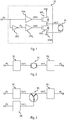
- Figure 1 shows a typical half-bridge arrangement 20 comprising two electronic switches SW 1 and SW 2 , such as n-channel power Field-Effect Transistor (FET), such as Metal-Oxide-Semiconductor Field-Effect Transistors (MOSFET), connected in series between a supply voltage Vdd and a ground GND.
- FET Field-Effect Transistor
- MOSFET Metal-Oxide-Semiconductor Field-Effect Transistors
- the switches SW 1 and SW 2 are closed alternatively in order to connect the output OUT of the half-bridge arrangement 20, i.e. the intermediate point between the switches SW 1 and SW 2 , either to the voltage Vdd or to ground GND.
- the half-bridge is driven as a function of two drive signals DRV 1 and DRV 2 , which are connected ( e.g. directly) to the control gates of the switches SW 1 and SW 2 , respectively.
- a high-side driver 200 1 is used to generate the drive signal DRV 1 for the high-side switch SW 1 as a function of a first control signal IN 1
- a low-side driver 200 2 is used to generate the drive signal DRV 2 for the low-side switch SW 2 as a function of a control signal IN 2
- the control signal IN 2 corresponds often to an inverted version of the signal IN 1 (or vice versa), i.e. the signal IN 2 is low when the signal IN 1 is high and vice versa.
- an inverter 202 which receives at input the signal IN 1 and provides at output the signal IN 2 .
- the output OUT of the half-bridge arrangement 20 may be used to drive a load.
- the half-bridge arrangement 20 drives a motor M 1 connected between the output OUT of the half-bridge arrangement 20 and ground GND.
- Figure 2 shows an example in which two half-bridge arrangements 20 a and 20 b are used to drive a linear motor M 2 , such as a voice coil motor, connected between the output OUT a of the first bridge arrangement 20 a and the output OUT b of the second bridge arrangement 20 b .
- a linear motor M 2 such as a voice coil motor
- the rotation direction of the motor M 2 may be controlled by applying appropriate control signals IN a and IN b to the half-bridge arrangements 20 a and 20 b .
- Figure 3 shows an example in which three half-bridge arrangements 20 a , 20 b and 20 c are used to drive a three-phase motor M 3 , such as a spindle motor, connected between the outputs OUT a , OUT b and OUT c of three half-bridge arrangements 20 a , 20 b and 20 c .
- a three-phase motor M 3 such as a spindle motor
- control signals may be PWM signals, i.e. signals with a fixed frequency and a variably duty cycle.
- PWM signals i.e. signals with a fixed frequency and a variably duty cycle.
- Italian patent application IT102015000046790 discloses a solution for generating two PWM signals which may be used, e.g., for generating the signals IN a and IN b in the solution shown in Figure 2 .
- Figure 4a shows in this respect a typical PWM signal, in particular the signal IN 1 , corresponding to a pulsed signal comprising a single pulse P for each switching cycle with duration or period T PWM , wherein the switch-on duration T ON1 of the pulse P may be variable.
- a Smart Power Device is used to generate the drive signals for the high side and low side switches SW 1 /SW 2 in order to drive, e.g., a three-phase BLDC motor.
- a typical SPD device is the integrated circuit (IC) STMicroelectronics L9907, as described e.g. in " L9907 - Automotive FET driver for 3 phase BLDC motor - Datasheet - production data", March 2017, DocID029666 Rev 1 , which is incorporated herein by reference.
- FIG 5 schematically shows the structure of such an IC 22.
- this IC 22 is able to receive at input six control signals IN 1 ..IN 6 and generate six drive signals DRV 1 ..DRV 6 .
- the IC 22 may be connected to a signal generator 30, such as a microcontroller, configured to generate the control signals IN 1 ..IN 6 .
- the IC 22 comprises three high side drivers 200 1 , 200 3 and 200 5 configured to generate respective drive signals DRV 1 , DRV 3 and DRV 5 for three high side switches SW 1 , SW 3 and SW 5 and three low side drivers 200 2 , 200 4 and 200 6 configured to generate respective drive signals DRV 2 , DRV 4 and DRV 6 for three low side switches SW 2 , SW 4 and SW 6 .
- such a SPD device 22 comprises also an electronic converter 204 configured to generate the supply voltage Vdd for the half-bridges as a function of a power supply, such as a battery voltage VBAT.
- a power supply such as a battery voltage VBAT.
- the IC 22 comprises differential amplifiers 206 arranged to measure the motor phase currents.
- the L9907 IC comprises two differential amplifiers 206 1 and 206 2 arranged to generate two measurement signals CS 1 and CS 2 by measuring the current flowing through two motor phases, e.g. by using respective shunt resistors RS 1 and RS 2 connected in series with a respective motor phase.
- the measurements signals CS 1 and CS 2 may then be provided to the circuit 30 which may calculate the current of the third motor phase via Kirchhoff's law.
- the circuit 30 may generate the six PWM signals IN 1 ..IN 6 for the inputs of the IC 22 and synchronously monitor the two measurement signals CS 1 , CS 2 at the output of the IC 22.
- the signal generator 30 generates for each half-bridge two separate control signals for the high side and the low side switches, e.g. signals IN 1 and IN 2 , while in the solution shown in Figure 1 has been used a single signal IN 1 and an inverter 202 in order to generate the complementary signal IN 2 .
- the signal generator 20 may again generate a control signal IN 2 having a given switching period corresponding usually to the switching period T PWM .
- the switch-on period T ON2 of the signal IN 2 may not correspond directly to the switch-off period T OFF1 of the signal IN 1 (as in Figure 1 ), but the signal generator 30 may introduce delays, i.e.:
- the delays T ONDT and T OFFDT may depend on the type of the electronic switches SW 1 and SW 2 , etc.
- one or more of the above objectives is achieved by means of a half-bridge driver circuit having the features specifically set forth in the claims that follow.
- Embodiments moreover concern a related related integrated circuit and system.
- the half-bridge driver circuit comprises (at least) two output terminals for providing a high side drive signal for a high side switch and a low side drive signal for a low side switch.
- the half-bridge driver circuit such as an integrated circuit, comprises a high side driver circuit configured to generate the high side drive signal as a function of a high side control signal and a low side driver circuit configured to generate the low side drive signal as a function of a low side control signal.
- a half-bridge driver circuit may be used to drive a single phase or multi-phase motor via a signal generator.
- the high side control signal and the low side control signals should be PWM signals having a given switching period, wherein the high side control signal has a given switch-on duration and the low side control signal has a first delay between the instant when the low side control signal goes to low and the instant when the high side control signal goes to high and a second delay between the instant when the high side control signal goes to low and the instant when the low side control signal goes to high.
- the signal generator could provide two PWM signals to the half-bridge driver circuit.
- the half-bridge driver circuit comprises an input terminal for receiving a control signal and a processing circuit configured to generate the high side control signal and the low side control signal as a function of the control signal.
- the control signal is not a traditional PWM signal, but the control signal is a periodic signal with a given switching period and having two pulses for each switching period. More specifically, the four edges of the two pulses are aligned with the four sequential instants:
- the processing circuit comprises thus an edge detector configured to generate a first signal in response to a first type of edge (e.g. a rising edge) in the control signal and a second signal in response to a second type of edge (e.g. a falling edge) in the control signal, wherein the second type of edge is opposed to the first type of edge.
- a first type of edge e.g. a rising edge
- a second type of edge e.g. a falling edge
- the first signal and the second signal are then processed by a state machine in order to generate the high side and low side control signals.
- the state machine is configured to:
- the processing circuit generates the high side control signal and the low side control signal as PWM signals, wherein the low side control signal corresponds to an inverted version of the high side control signal with the first delay between the falling edge of the low side control signal and a following rising edge of the high side control signal and with the second delay between the falling edge of the high side control signal and the following rising edge of the low side control signal.
- the first type of edge is a rising edge
- the second type of edge is a falling edge
- the duration of the first delay corresponds to the duration of the first pulse of the control signal
- the duration of the second delay corresponds to the duration of the second pulse of the control signal.
- the state machine may comprise four states for implementing the above four transitions, i.e. one state for each transition.
- the state machine may also comprise only three states for implementing the above four transitions, wherein a given state is used for both the first and the second delay.
- the state machine may receive a synchronization signal, which is used to decide whether the state machine should proceed from the given state to either the state for switching the high side control signal to high or the state for switching the low side control signal to high.
- the state machine is configured to proceed to one of the states in response to a reset signal.
- the synchronization signal and/or the reset signal may be provided to the half-bride driver circuit via the signal generator, which thus may synchronize (possibly for each switching cycle) the state machine with the control signal.
- the present disclosure relates to a half-bridge driver circuit, such as a half-bridge driver IC.
- the signal generation circuit 30, such as a microcontroller, is configured to generate six PWM signals IN 1 ..IN 6 , which are provided at input to a driver IC 22.
- the various outputs OUT a , OUT b and OUT c are sequentially connected to the supply voltage Vdd (and Ground GND ), as described e.g. in document " AN1088 - APPLICATION NOTE - L6234 THREE PHASE MOTOR DRIVER", STMicroelectronics, April 2001 , which is incorporated herein by reference.
- a driver circuit 22a which may operate with a reduced number of control signals, i.e. the signal generator 30, such as a microcontroller, has to generate less control signals.
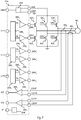
- Figure 7 shows an embodiment of a driver circuit 22a, such as an integrated circuit, configured to receive at input a single control signal CTR for each half-bridge, and the driver circuit 22a is configured to generate a high side drive signal for a respective high side switch and a low side drive signal for a respective low side switch as a function of the control signal CTR.
- the driver circuit 22a comprises a respective high side drive circuit for generating the high side drive signal as a function of a high side control signal and a low side drive circuit for generating the low side drive signal as a function of a low side control signal.
- the driver circuit 22a comprises a processing circuit 208 configured to generate the high side control signal and the low side drive signal for the high side and low side drivers as a function of the respective control signal CTR.
- the driver circuit 22a is again configured to drive three half bridges. Accordingly, the driver circuit is configured to receive three control signals CTR 1 , CTR 2 and CTR 3 and generate respective drive signals DRV 1 , DRV 3 and DRV 5 for three high side switches SW 1 , SW 3 and SW 5 and respective drive signals DRV 2 , DRV 4 and DRV 6 for three low side switches SW 2 , SW 4 and SW 6 .
- the driver circuit 22a comprises three circuits 208 1 , 208 2 and 208 3 configured to generate for each control signals CTR 1 , CTR 2 and CTR 3 a respective high side control signal IN 1 , IN 3 and IN 5 and a respective low side control signal IN 2 , IN 4 and IN 6 .
- the driver circuit 22a for generating a drive signal DRV as a function of the control signal IN may correspond to the architecture of the circuit 22 shown in Figure 5 and the respective description fully applies.
- the driver circuit 22a comprises three high side drivers 200 1 , 200 3 and 200 5 configured to generate the drive signals DRV 1 , DRV 3 and DRV 5 for three high side switches SW 1 , SW 3 and SW 5 and three low side drivers 200 2 , 200 4 and 200 6 configured to generate the drive signals DRV 2 , DRV 4 and DRV 6 for three low side switches SW 2 , SW 4 and SW 6 .
- the driver circuit 22a may also comprise the electronic converter 204 configured to generate the supply voltage Vdd and/or the differential amplifiers 206 for measuring the current flowing through the motor phases.
- the driver circuit 22a could also be configured to drive less ( e.g. one or two) or more half-bridges.
- the driver circuit 22a may also be used to drive a motor M 1 connected between the output of a half-bridge and ground GND (see Figure 1 ).
- the driver circuit 22a may also be used to drive a motor M 2 connected between the outputs of two half-bridge (see Figure 2 ).
- the driver circuit 22a may be configured to drive a single-phase motor via one or two half-bridges, or a multi-phase motor (e.g. a three-phase motor) via a corresponding number of half-bridges.
- the driver circuit 22a comprises for each half-bridge a single input for receiving a respective control signal CTR and a circuit 208 configured to generate a respective high side control signal (e.g. signal IN 1 ) and a respective low side control signal ( e.g. signal IN 2 ), which are provided to a high side driver ( e.g. 200 1 ) and a low side driver ( e.g. 200 2 ), respectively.
- a respective high side control signal e.g. signal IN 1
- a respective low side control signal e.g. signal IN 2
- Figure 8 shows a first embodiment of the circuit 208, such as the circuit 208 1 configured to generate the signals IN 1 and IN 2 as a function of the control signal CTR 1 .
- the same architecture may be used also for the other circuits 208.
- the circuit 208 1 comprises a rising edge detector 2080 configured to generate a signal RE by analyzing the control signal CTR 1 , i.e. the signal RE indicates a rising edge in the signal CTR 1 .
- the circuit 208 1 comprises a falling edge detector 2082 configured to generate a signal FE by analyzing the control signal CTR 1 , i.e. the signal FE indicates a falling edge in the signal CTR 1 .
- the edge detectors 2080 and 2082 may also be combined in a single edge detector providing both signals RE and FE.
- the signal RE and FE are provided to a (finite) state machine 2084 configured to generate the high side control signal IN 1 and the low side control signal IN 2 .
- Figure 9 shows an embodiment of the operation of the processing circuit 208.
- control signal CTR 1 is not a traditional PWM signal, but the signal generator 30 is configured to generate a control signal CTR 1 comprising pulses in correspondence to the delays T ONDT and T OFFDT , i.e. the signal CTR 1 is a periodic signal with a given duration T PWM comprising:
- the signal CTR 1 comprises:
- the edge detector 2080 is configured to generate a signal RE indicative of a first type of edge (e.g. rising in the embodiment considered) and the edge detector 2082 is configured to generate a signal FE indicative of a second type of edge opposed to the first type of edge ( e.g. falling in the embodiment considered).
- the edge detectors 2080 and 2082 may be implemented with asynchronous or synchronous edge detectors.
- a synchronous edge detector may sample the signal CTR 1 in order to determine a bit sequence. Accordingly, a rising edge may be detected when the bit sequence has the value "01" for a two-bit sequence, or "001" or "011” for a three-bit sequence, etc. Similarly, a falling edge may be detected when the bit sequence has the value "10" for a two-bit sequence, or "100" or "110” for a three-bit sequence, etc.
- Figure 10 shows an embodiment of the state machine 2084, which e.g. may be implemented with a sequential logic circuit.
- the state machine comprises at least four states S1..S4, in particular:
- the state machine 2084 may move to one of the states S1..S4.
- the state machine may move to the states S1 or S3, where the half-bridge switches are switched off, or preferably the state S4, where only the low side switch is closed.
- the circuit 208 may be configured to render the initial state after a reset programmable.
- the driver circuit 22a may comprise a communication interface 210 connected to one or more interface terminals IF (see Figure 7 ).
- the communication interface 210 may be serial communication interface, such as Inter-Integrated Circuit (I2C), Serial Peripheral Interface bus (SPI), or Universal asynchronous receiver-transmitter (UART).
- I2C Inter-Integrated Circuit
- SPI Serial Peripheral Interface bus
- UART Universal asynchronous receiver-transmitter
- the state machine in response to the rising and falling edges in the control signal CTR 1 , the state machine evolves sequentially through the states S1..S4.
- Figure 11 shows a possible implementation of the state machine 2084.
- the state machine is implemented with a Moore state machine comprising:
- the state register 2086 may support a reset, e.g. via a reset signal RST, which sets the content of the register 2086 to a reset value, e.g. corresponding to the bit sequence associated with the state S4.
- the register 2086 has three bits and the following encoding is used for the states:
- the circuit 2090 may select the second bit of state S as the control signal IN 1 and the third/last bit of state S as the control signal IN 2 .
- the state machine 2084 may also be configured to monitor incongruent input signals. For example, the state machine may monitor in the states S1 and S3 whether the signal RE is set and possibly proceed to an error state. Similarly, the state machine may monitor in the states S3 and S4 whether the signal FE is set and possibly proceed to an error state.
- the state machine 2084 may monitor the state signal S in order to determine incongruent states. For example, in the embodiment considered, the states “011” and “111" may be incongruent states, because the last two bits should not be set contemporaneously to "1". Also in this case, the state machine may proceed to an error state.
- the state machine 2084 performs transitions in response to the signals RE and FE (i.e. in response to the rising and falling edges in the signal the signal CTR 1 ), thereby sequentially passing through the states S1..S4 starting from a given reset state.
- the state machine may skip one of the two pulses in the control signal CTR 1 resulting in an inversion of the control signals IN 1 and IN 2 , i.e. an incorrect driving of the half-bridge.
- the circuit 208 may comprise an internal watchdog timer.
- the internal watchdog timer may be reset by the signal RE (or by the signal FE ) and it communicates an error if the timer reaches a programmable threshold.
- the threshold is set via the interface 210.
- the threshold should be greater than MAX( T PWM - T ONDT , T PWM - T OFFDT ) and smaller than T PWM .
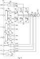
- Figure 12 shows a further embodiment of the driver circuit 22a comprising an additional terminal for receiving a further control/synchronization signal CTR 0 .
- control signal CTR 0 is arranged to identify the respective switching cycle.
- control signal CTR 0 may be a left-aligned PWM signal having again the switching period T PWM .
- the control signal CTR 0 may comprise a short pulse (with a duration being smaller than T OFFa ) and the state machine 2084 may be configured to move to the state S4 in response to the control signal CTR 0 , e.g. by using the signal CTR 0 as reset signal RST for the state register 2086.
- control signal CTR 0 may be a left-aligned PWM signal having a switch-on duration being greater than T OFFa and smaller than T OFFa + T ON , such as a PWM signal with 50% duty cycle.
- each state machine may determine whether a given (rising or falling) edge belongs to the interval T ONDT or T OFFDT .
- the state machine may directly use the logic level of the control signal CTR 0 in order to determine e.g.:
- the states S1 and S3 have been combined in a single state S1'.
- the state machine is configured to remain in the state S1 until a new (falling) edge is signaled by the circuit 2082 via the signal FE. Accordingly, once the signal FE is set, the state machine proceeds either:
- control/synchronization signal CTR 0 may have inverted logic levels.
- a single control/synchronization signal CTR 0 may be used for all circuits 208.
- a driver circuit 22a for three half-bridges may receive at input four control signals instead of the six control signals shown in Figure 5 in the context of prior-art solutions.
Landscapes
- Engineering & Computer Science (AREA)
- Power Engineering (AREA)
- Computer Hardware Design (AREA)
- Physics & Mathematics (AREA)
- Computing Systems (AREA)
- General Engineering & Computer Science (AREA)
- Mathematical Physics (AREA)
- Inverter Devices (AREA)
- Electronic Switches (AREA)
- Control Of Direct Current Motors (AREA)
Abstract
Description
- Embodiments of the present disclosure relate to half-bridge driver circuits.
- In automotive applications the use of Direct Current (DC) or Brushless DC (BLDC) motors for fan, pump or actuator applications is very common with the trend of replacing the traditional DC with BLDC motors. In most automotive applications, detection of fault conditions of the BLDC motor and the control electronics is mandatory. For this reason, the control electronics should be able to identify a possible fault condition and then apply counter measures, e.g., in order to protect the system. Often the detected fault condition is reported to a system controller and may be accessible via the diagnosis interface of the automobile for further service investigations.
- As disclosed, e.g., in the Italian patent application
IT102016000009376 - For example,
Figure 1 shows a typical half-bridge arrangement 20 comprising two electronic switches SW1 and SW2, such as n-channel power Field-Effect Transistor (FET), such as Metal-Oxide-Semiconductor Field-Effect Transistors (MOSFET), connected in series between a supply voltage Vdd and a ground GND. - Usually, the switches SW1 and SW2 are closed alternatively in order to connect the output OUT of the half-
bridge arrangement 20, i.e. the intermediate point between the switches SW1 and SW2, either to the voltage Vdd or to ground GND. For this purpose, the half-bridge is driven as a function of two drive signals DRV1 and DRV2, which are connected (e.g. directly) to the control gates of the switches SW1 and SW2, respectively. Specifically, in order to correctly drive the control gates, often a high-side driver 2001 is used to generate the drive signal DRV1 for the high-side switch SW1 as a function of a first control signal IN1, and a low-side driver 2002 is used to generate the drive signal DRV2 for the low-side switch SW2 as a function of a control signal IN2. The control signal IN2 corresponds often to an inverted version of the signal IN1 (or vice versa), i.e. the signal IN2 is low when the signal IN1 is high and vice versa. For example, inFigure 1 is used aninverter 202 which receives at input the signal IN1 and provides at output the signal IN2. - The output OUT of the half-
bridge arrangement 20 may be used to drive a load. For example, inFigure 1 , the half-bridge arrangement 20 drives a motor M1 connected between the output OUT of the half-bridge arrangement 20 and ground GND. - Conversely,
Figure 2 shows an example in which two half-bridge arrangements first bridge arrangement 20a and the output OUTb of thesecond bridge arrangement 20b. As well known to those of skill in the art, in this case, also the rotation direction of the motor M2 may be controlled by applying appropriate control signals INa and INb to the half-bridge arrangements - Finally,
Figure 3 shows an example in which three half-bridge arrangements bridge arrangements - As mentioned before, the control signals may be PWM signals, i.e. signals with a fixed frequency and a variably duty cycle. For example, Italian patent application
IT102015000046790 Figure 2 . -
Figure 4a shows in this respect a typical PWM signal, in particular the signal IN1, corresponding to a pulsed signal comprising a single pulse P for each switching cycle with duration or period TPWM, wherein the switch-on duration TON1 of the pulse P may be variable. Generally, the pulse P is not necessarily at the beginning of each switching cycle, but each switching cycle may comprise an initial switch-off period TOFFa before the pulse P and a final switch-off period TOFFb after the pulse P, with:


- For example, in most high-end automotive applications (e.g., Electric Power Steering, Electric Turbo Charge, etc.), a Smart Power Device (SPD) is used to generate the drive signals for the high side and low side switches SW1/SW2 in order to drive, e.g., a three-phase BLDC motor. A typical SPD device is the integrated circuit (IC) STMicroelectronics L9907, as described e.g. in " L9907 - Automotive FET driver for 3 phase BLDC motor - Datasheet - production data", March 2017, DocID029666 , which is incorporated herein by reference.
-
Figure 5 schematically shows the structure of such anIC 22. Specifically, thisIC 22 is able to receive at input six control signals IN1..IN6 and generate six drive signals DRV1..DRV6. For example, as shown inFigure 6 , theIC 22 may be connected to asignal generator 30, such as a microcontroller, configured to generate the control signals IN1..IN6 . Accordingly, theIC 22 comprises threehigh side drivers low side drivers - Often such a
SPD device 22 comprises also anelectronic converter 204 configured to generate the supply voltage Vdd for the half-bridges as a function of a power supply, such as a battery voltage VBAT. - Moreover, often the
IC 22 comprisesdifferential amplifiers 206 arranged to measure the motor phase currents. Specifically, the L9907 IC comprises twodifferential amplifiers Figure 6 , the measurements signals CS1 and CS2 may then be provided to thecircuit 30 which may calculate the current of the third motor phase via Kirchhoff's law. Specifically, thecircuit 30 may generate the six PWM signals IN1..IN6 for the inputs of theIC 22 and synchronously monitor the two measurement signals CS1, CS2 at the output of theIC 22. - Accordingly, in the solution shown in
Figure 6 , thesignal generator 30 generates for each half-bridge two separate control signals for the high side and the low side switches, e.g. signals IN1 and IN2, while in the solution shown inFigure 1 has been used a single signal IN1 and aninverter 202 in order to generate the complementary signal IN2. Specifically, as shown inFigure 4b , in this way thesignal generator 20 may again generate a control signal IN2 having a given switching period corresponding usually to the switching period TPWM. However, the switch-on period TON2 of the signal IN2 may not correspond directly to the switch-off period TOFF1 of the signal IN1 (as inFigure 1 ), but thesignal generator 30 may introduce delays, i.e.: - a delay TONDT between the instant when the low side control signal IN2 goes to low and the instant when the high side control signal IN1 goes to high; and
- a delay TOFFDT between the instant when the high side control signal IN1 goes to low and the instant when the low side control signal IN2 goes to high.
- Accordingly, usually the
signal generator 30 is configured to generate a control signal IN2 with:

- For example, the delays TONDT and TOFFDT may depend on the type of the electronic switches SW1 and SW2, etc.
- Thus, the solution shown in
Figure 6 is more flexible, but additional control signals are required, rendering the solution more complex. - In view of the above, various embodiments provide solutions for generating the drive signals for one or more half-bridges.
- According to one or more embodiments, one or more of the above objectives is achieved by means of a half-bridge driver circuit having the features specifically set forth in the claims that follow. Embodiments moreover concern a related related integrated circuit and system.
- The claims are an integral part of the technical teaching of the disclosure provided herein.
- As mentioned before, various embodiments of the present disclosure relate to a half-bridge driver circuit. Specifically, the half-bridge driver circuit comprises (at least) two output terminals for providing a high side drive signal for a high side switch and a low side drive signal for a low side switch. In various embodiments, the half-bridge driver circuit, such as an integrated circuit, comprises a high side driver circuit configured to generate the high side drive signal as a function of a high side control signal and a low side driver circuit configured to generate the low side drive signal as a function of a low side control signal. For example, such a half-bridge driver circuit may be used to drive a single phase or multi-phase motor via a signal generator.
- In various embodiments, in order to correctly drive the half-bridge, the high side control signal and the low side control signals should be PWM signals having a given switching period, wherein the high side control signal has a given switch-on duration and the low side control signal has a first delay between the instant when the low side control signal goes to low and the instant when the high side control signal goes to high and a second delay between the instant when the high side control signal goes to low and the instant when the low side control signal goes to high. Accordingly, as described in the foregoing, the signal generator could provide two PWM signals to the half-bridge driver circuit. Conversely, in various embodiments, the half-bridge driver circuit comprises an input terminal for receiving a control signal and a processing circuit configured to generate the high side control signal and the low side control signal as a function of the control signal. Specifically, in various embodiments, the control signal is not a traditional PWM signal, but the control signal is a periodic signal with a given switching period and having two pulses for each switching period. More specifically, the four edges of the two pulses are aligned with the four sequential instants:
- 1) when the low side control signal should be switched-off,
- 2) after the first delay, when the high side control signal should be switched-on,
- 3) after the switch-on duration of the high side control signal, when the high side control signal should be switched-off; and
- 4) after the second delay, when the low side control signal should be switched-on.
- In various embodiments, the processing circuit comprises thus an edge detector configured to generate a first signal in response to a first type of edge (e.g. a rising edge) in the control signal and a second signal in response to a second type of edge (e.g. a falling edge) in the control signal, wherein the second type of edge is opposed to the first type of edge.
- In various embodiments, the first signal and the second signal are then processed by a state machine in order to generate the high side and low side control signals. Specifically, in various embodiments, the state machine is configured to:
- in response to the first signal, set the high side control signal and the low side control signal to a first logic level (e.g. low);
- in response to the second signal, set the high side control signal to a second logic level (e.g. high) and the low side control signal to the first logic level;
- in response to the first signal, set the high side control signal and the low side control signal to the first logic level; and
- in response to the second signal, set the high side control signal to the first logic level and the low side control signal to the second logic level.
- Accordingly, by using a control signal comprising a first and a second pulse for each switching cycle, the processing circuit generates the high side control signal and the low side control signal as PWM signals, wherein the low side control signal corresponds to an inverted version of the high side control signal with the first delay between the falling edge of the low side control signal and a following rising edge of the high side control signal and with the second delay between the falling edge of the high side control signal and the following rising edge of the low side control signal. For example, when the first type of edge is a rising edge and the second type of edge is a falling edge, the duration of the first delay corresponds to the duration of the first pulse of the control signal and the duration of the second delay corresponds to the duration of the second pulse of the control signal.
- In various embodiments, the state machine may comprise four states for implementing the above four transitions, i.e. one state for each transition. Alternatively, the state machine may also comprise only three states for implementing the above four transitions, wherein a given state is used for both the first and the second delay. In this case, the state machine may receive a synchronization signal, which is used to decide whether the state machine should proceed from the given state to either the state for switching the high side control signal to high or the state for switching the low side control signal to high.
- In various embodiments, the state machine is configured to proceed to one of the states in response to a reset signal.
- Generally, the synchronization signal and/or the reset signal may be provided to the half-bride driver circuit via the signal generator, which thus may synchronize (possibly for each switching cycle) the state machine with the control signal.
- Embodiments of the present disclosure will now be described with reference to the annexed drawings, which are provided purely by way of non-limiting example and in which:
-
Figures 1, 2, 3 and4 show solutions for driving a motor; -
Figures 5 and6 show an example of a half-bridge driver; -
Figure 7 shows an embodiment of a half-bridge driver circuit comprising a processing circuit configured to generate high side and low side control signals as a function of a control signal; -
Figures 8, 9 ,10 and 11 show an embodiment of the processing circuit ofFigure 7 ; -
Figure 12 shows a further embodiment of a half-bridge driver circuit comprising a processing circuit configured to generate high side and low side control signals as a function of a control signal; and -
Figure 13 show an embodiment of the processing circuit ofFigure 12 . - In the following description, numerous specific details are given to provide a thorough understanding of embodiments. The embodiments can be practiced without one or several specific details, or with other methods, components, materials, etc. In other instances, well-known structures, materials, or operations are not shown or described in detail to avoid obscuring aspects of the embodiments.
- Reference throughout this specification to "one embodiment" or "an embodiment" means that a particular feature, structure, or characteristic described in connection with the embodiment is included in at least one embodiment. Thus, the appearances of the phrases "in one embodiment" or "in an embodiment" in various places throughout this specification are not necessarily all referring to the same embodiment. Furthermore, the particular features, structures, or characteristics may be combined in any suitable manner in one or more embodiments.
- The headings provided herein are for convenience only and do not interpret the scope or meaning of the embodiments.
- In the following
Figures 7 to 13 parts, elements or components which have already been described with reference toFigures 1 to 6 are denoted by the same references previously used in such Figures; the description of such previously described elements will not be repeated in the following in order not to overburden the present detailed description. - As mentioned in the foregoing, the present disclosure relates to a half-bridge driver circuit, such as a half-bridge driver IC.
- As described in the foregoing, in the architecture shown in
Figures 5 and6 , thesignal generation circuit 30, such as a microcontroller, is configured to generate six PWM signals IN1..IN6, which are provided at input to adriver IC 22. For example, when driving a three-phase motor M3 as shown inFigure 3 , the various outputs OUTa, OUTb and OUTc are sequentially connected to the supply voltage Vdd (and Ground GND), as described e.g. in document "AN1088 - APPLICATION NOTE - L6234 THREE PHASE MOTOR DRIVER", STMicroelectronics, April 2001, which is incorporated herein by reference. - However, this solution is complex, because two control signals have to be provided to the
driver circuit 22 for each half-bridge. For example, this may result in additional complexity, when thesignal generator 30 and/or thedriver circuit 22 should also monitor the PWM control signals for detecting errors. For example, a possible solution for monitoring PWM signals is described in Italian patent applicationIT102016000049920 - Accordingly, when using such a solution in the
signal generator 30 and/ordriver circuit 22, six error detection circuits would be required. - Various embodiments of the present disclosure relate thus to a
driver circuit 22a, which may operate with a reduced number of control signals, i.e. thesignal generator 30, such as a microcontroller, has to generate less control signals. - For example,
Figure 7 shows an embodiment of adriver circuit 22a, such as an integrated circuit, configured to receive at input a single control signal CTR for each half-bridge, and thedriver circuit 22a is configured to generate a high side drive signal for a respective high side switch and a low side drive signal for a respective low side switch as a function of the control signal CTR. Specifically, in the embodiment considered, thedriver circuit 22a comprises a respective high side drive circuit for generating the high side drive signal as a function of a high side control signal and a low side drive circuit for generating the low side drive signal as a function of a low side control signal. Accordingly, in various embodiment, thedriver circuit 22a comprises aprocessing circuit 208 configured to generate the high side control signal and the low side drive signal for the high side and low side drivers as a function of the respective control signal CTR. - For example, in the embodiment considered, the
driver circuit 22a is again configured to drive three half bridges. Accordingly, the driver circuit is configured to receive three control signals CTR1, CTR2 and CTR3 and generate respective drive signals DRV1, DRV3 and DRV5 for three high side switches SW1, SW3 and SW5 and respective drive signals DRV2, DRV4 and DRV6 for three low side switches SW2, SW4 and SW6. - More specifically, the
driver circuit 22a comprises threecircuits - Generally, the implementation of the
driver circuit 22a for generating a drive signal DRV as a function of the control signal IN may correspond to the architecture of thecircuit 22 shown inFigure 5 and the respective description fully applies. For example, in the embodiment considered, thedriver circuit 22a comprises threehigh side drivers low side drivers driver circuit 22a may also comprise theelectronic converter 204 configured to generate the supply voltage Vdd and/or thedifferential amplifiers 206 for measuring the current flowing through the motor phases. - Accordingly, in the embodiment considered, the
driver circuit 22a is arranged to drive N = 3 half-bridges, wherein thedriver circuit 22a comprises for each half-bridge a respective high side driver and a respective low side driver. Generally, thedriver circuit 22a could also be configured to drive less (e.g. one or two) or more half-bridges. - Moreover, even though being arranged to drive N = 3 half-bridges, the
driver circuit 22a may also be used to drive a motor M1 connected between the output of a half-bridge and ground GND (seeFigure 1 ). For example, for this purpose, only two drive signals (e.g. DRV1 and DRV2 ) of thedriver circuit 22a may be used. Similarly, thedriver circuit 22a may also be used to drive a motor M2 connected between the outputs of two half-bridge (seeFigure 2 ). For example, for this purpose, only four drive signals (e.g. DRV1...DRV4 ) of thedriver circuit 22a may be used. Thus, generally thedriver circuit 22a may be configured to drive a single-phase motor via one or two half-bridges, or a multi-phase motor (e.g. a three-phase motor) via a corresponding number of half-bridges. - As described in the foregoing, in various embodiments, the
driver circuit 22a comprises for each half-bridge a single input for receiving a respective control signal CTR and acircuit 208 configured to generate a respective high side control signal (e.g. signal IN1 ) and a respective low side control signal (e.g. signal IN2 ), which are provided to a high side driver (e.g. 2001) and a low side driver (e.g. 2002), respectively. -
Figure 8 shows a first embodiment of thecircuit 208, such as thecircuit 2081 configured to generate the signals IN1 and IN2 as a function of the control signal CTR1. Generally, the same architecture may be used also for theother circuits 208. - Specifically, in the embodiment considered, the
circuit 2081 comprises a risingedge detector 2080 configured to generate a signal RE by analyzing the control signal CTR1, i.e. the signal RE indicates a rising edge in the signal CTR1. Moreover, thecircuit 2081 comprises a fallingedge detector 2082 configured to generate a signal FE by analyzing the control signal CTR1, i.e. the signal FE indicates a falling edge in the signal CTR1. Generally, theedge detectors state machine 2084 configured to generate the high side control signal IN1 and the low side control signal IN2. -
Figure 9 shows an embodiment of the operation of theprocessing circuit 208. - Specifically, in the embodiment considered, the control signal CTR1 is not a traditional PWM signal, but the
signal generator 30 is configured to generate a control signal CTR1 comprising pulses in correspondence to the delays TONDT and TOFFDT, i.e. the signal CTR1 is a periodic signal with a given duration TPWM comprising: - a first pulse with duration TONDT, wherein the first pulse starts after the switch-off duration (TOFFa - TONDT ) from the beginning of the corresponding PWM cycle; and
- a second pulse with duration TOFFDT, wherein the second pulse starts after the switch-on duration TON from the end of the first pulse.
- Accordingly, assuming that the PWM cycle starts at an instant t 0, the signal CTR1 comprises:
- a rising edge at an instant t 1 = TOFFa - TONDT;
- a falling edge at an instant t 2 = t 1 + TONDT = TOFFa;
- a rising edge at an instant t 3 = t 2 + TON; and
- a falling edge at an instant t 4 = t 3 + TOFFDT.
- Generally, the signal CTR1 and thus the above edges may also be inverted. Accordingly, generally, the
edge detector 2080 is configured to generate a signal RE indicative of a first type of edge (e.g. rising in the embodiment considered) and theedge detector 2082 is configured to generate a signal FE indicative of a second type of edge opposed to the first type of edge (e.g. falling in the embodiment considered). - Generally, the
edge detectors -
Figure 10 shows an embodiment of thestate machine 2084, which e.g. may be implemented with a sequential logic circuit. - Specifically, in the embodiment considered, the state machine comprises at least four states S1..S4, in particular:
- state S1 used to generate the control signals IN1 /IN2 during the duration TONDT, i.e. IN1 = "0" and IN2 = "0";
- state S2 used to generate the control signals IN1 /IN2 during the duration TON , i.e. IN1 = "1" and IN2 = "0";
- state S3 used to generate the control signals IN1 /IN2 during the duration TOFFDT, i.e. IN1 = "0" and IN2 = "0";
- state S4 used to generate the control signals IN1 /IN2 during the remaining duration TOFF (in particular the duration TOFF - TOFFDT - TONDT ), i.e. IN1 = "0" and IN2 = "1".
- In various embodiments, after a reset of the
circuit 208, thestate machine 2084 may move to one of the states S1..S4. For example, based on the application, the state machine may move to the states S1 or S3, where the half-bridge switches are switched off, or preferably the state S4, where only the low side switch is closed. In various embodiments, thecircuit 208 may be configured to render the initial state after a reset programmable. For example, in various embodiments, thedriver circuit 22a may comprise acommunication interface 210 connected to one or more interface terminals IF (seeFigure 7 ). For example, thecommunication interface 210 may be serial communication interface, such as Inter-Integrated Circuit (I2C), Serial Peripheral Interface bus (SPI), or Universal asynchronous receiver-transmitter (UART). - The operation of the
state machine 2084 will now be described at a typical switching cycle, assuming the state machine is in the state S4 at the beginning of a new switching cycle, i.e. instant t 0. Specifically, in the state S4, the high side switch SW1 is opened (IN1 = "0") and the low side switch SW2 is closed (IN2 = "1"). - The state machine is configured to remain in the state S4 until a new (rising) edge is signaled by the
circuit 2080 via the signal RE (instant t1 ). Accordingly, once the signal RE is set, the state machine proceeds to the state S1, in which the high side switch SW1 and the low side switch SW2 are opened (IN1 = "0" and IN2 = "0") . - The state machine is configured to remain in the state S1 until a new (falling) edge is signaled by the
circuit 2082 via the signal FE (instant t2 ). Accordingly, once the signal FE is set, the state machine proceeds to the state S2, in which the high side switch SW1 is closed (IN1 = "1") and the low side switch SW2 is opened (IN2 = "0") . - The state machine is configured to remain in the state S2 until a new (rising) edge is signaled by the
circuit 2080 via the signal RE (instant t3 ). Accordingly, once the signal RE is set, the state machine proceeds to the state S3, in which the high side switch SW1 and the low side switch SW2 are opened (IN1 = "0" and IN2 = "0") . - Finally, the state machine is configured to remain in the state S3 until a new (falling) edge is signaled by the
circuit 2082 via the signal FE (instant t4 ). Accordingly, once the signal FE is set, the state machine proceeds again to the state S4, in which the high side switch SW1 is opened (IN1 = "0") and the low side switch SW2 is closed (IN2 = "1") . - Accordingly, in response to the rising and falling edges in the control signal CTR1, the state machine evolves sequentially through the states S1..S4.
- For example,
Figure 11 shows a possible implementation of thestate machine 2084. - In the embodiment considered, the state machine is implemented with a Moore state machine comprising:
- a
state register 2086 configured to store the value of a current state S, wherein the value of a next states NS is stored in response to a clock signal CLK; - a combinational logic circuit configured to generating the next state signal NS as a function of the current state S (at the output of the states register 2086) and the input signals, i.e. signals RE and FE; and
- a
combinational logic circuit 2090 configured to generating the output signals IN1 and IN2 as a function of the current state S (at the output of the states register 2086). - Moreover, as mentioned before, the
state register 2086 may support a reset, e.g. via a reset signal RST, which sets the content of theregister 2086 to a reset value, e.g. corresponding to the bit sequence associated with the state S4. - For example, in various embodiments, the
register 2086 has three bits and the following encoding is used for the states: - S1: S = "000";
- S2: 5 = "110";
- S3: S = "100"; and
- S4: S = "001".
- For example, by using this encoding, the
circuit 2090 may select the second bit of state S as the control signal IN1 and the third/last bit of state S as the control signal IN2. - Generally, the
state machine 2084 may also be configured to monitor incongruent input signals. For example, the state machine may monitor in the states S1 and S3 whether the signal RE is set and possibly proceed to an error state. Similarly, the state machine may monitor in the states S3 and S4 whether the signal FE is set and possibly proceed to an error state. - Similarly, the
state machine 2084 may monitor the state signal S in order to determine incongruent states. For example, in the embodiment considered, the states "011" and "111" may be incongruent states, because the last two bits should not be set contemporaneously to "1". Also in this case, the state machine may proceed to an error state. - Accordingly, in the embodiment considered, the
state machine 2084 performs transitions in response to the signals RE and FE (i.e. in response to the rising and falling edges in the signal the signal CTR1 ), thereby sequentially passing through the states S1..S4 starting from a given reset state. - However, when loosing synchronization, e.g. due to errors/glitches in the control signal CTR the state machine may skip one of the two pulses in the control signal CTR1 resulting in an inversion of the control signals IN1 and IN2, i.e. an incorrect driving of the half-bridge. To detect this type of fault, different counter measures can be implemented. For example, in various embodiments, the
circuit 208 may comprise an internal watchdog timer. For example, the internal watchdog timer may be reset by the signal RE (or by the signal FE) and it communicates an error if the timer reaches a programmable threshold. For example, in various embodiment, the threshold is set via theinterface 210. Generally, the threshold should be greater than MAX(TPWM - TONDT, TPWM - TOFFDT ) and smaller than TPWM. -
Figure 12 shows a further embodiment of thedriver circuit 22a comprising an additional terminal for receiving a further control/synchronization signal CTR0. - Specifically, the control signal CTR0 is arranged to identify the respective switching cycle.
- For example, the control signal CTR0 may be a left-aligned PWM signal having again the switching period TPWM. For example, the control signal CTR0 may comprise a short pulse (with a duration being smaller than TOFFa ) and the
state machine 2084 may be configured to move to the state S4 in response to the control signal CTR0, e.g. by using the signal CTR0 as reset signal RST for thestate register 2086. - Alternatively, the control signal CTR0 may be a left-aligned PWM signal having a switch-on duration being greater than TOFFa and smaller than TOFFa + TON, such as a PWM signal with 50% duty cycle. Accordingly, by providing the control signal CTR0 to the
control circuits 208, in particular thestate machines 2084, each state machine may determine whether a given (rising or falling) edge belongs to the interval TONDT or TOFFDT. For example, in this case, the state machine may directly use the logic level of the control signal CTR0 in order to determine e.g.: - whether the
state machine 2084 should proceed either to the state S1 (e.g. CTR0 = "1") or S3 (e.g. CTR0 = "0") in response to a rising edge (RE = "1"); and - whether the
state machine 2084 should proceed either to the state S2 (e.g. CTR0 = "1") or S4 (e.g. CTR0 = "0") in response to a falling edge (FE = "1"). - For example, a modified state machine is shown in
Figure 13 . - Specifically, in the embodiment considered, the states S1 and S3 have been combined in a single state S1'.
- For example, again assuming that the
state machine 2084 is in the state S4 at the beginning of a new switching cycle, i.e. instant t 0, the high side switch SW1 is opened (IN1 = "0") and the low side switch SW2 is closed (IN2 = "1") . - The state machine is configured to remain in the state S4 until a new (rising) edge is signaled by the
circuit 2080 via the signal RE. Accordingly, once the signal RE is set, the state machine proceeds to the state S1, in which the high side switch SW1 and the low side switch SW2 are opened (IN1 = "0" and IN2 = "0") . - The state machine is configured to remain in the state S1 until a new (falling) edge is signaled by the
circuit 2082 via the signal FE. Accordingly, once the signal FE is set, the state machine proceeds either: - to the state S2 when the signal CTR0 is set; or
- to the state S4 when the signal CTR0 is not set.
- Specifically, in the state S2 the high side switch SW1 is again closed (IN1 = "1") and the low side switch SW2 is opened (IN2 = "0") .
- Generally, also the control/synchronization signal CTR0 may have inverted logic levels. Moreover, a single control/synchronization signal CTR0 may be used for all
circuits 208. For example, in this case, adriver circuit 22a for three half-bridges may receive at input four control signals instead of the six control signals shown inFigure 5 in the context of prior-art solutions. - Of course, without prejudice to the principle of the invention, the details of construction and the embodiments may vary widely with respect to what has been described and illustrated herein purely by way of example, without thereby departing from the scope of the present invention, as defined by the ensuing claims.
Claims (11)
- A half-bridge driver circuit (22a) comprising:- two output terminals for providing a high side drive signal (DRV1 ) for a high side switch (SW1) and a low side drive signal (DRV2 ) for a low side switch (SW2);- a high side driver circuit (2001) configured to generate said high side drive signal (DRV1 ) as a function of a high side control signal (IN1 );- a low side driver circuit (2002) configured to generate said low side drive signal (DRV2 ) as a function of a low side control signal (IN2 );- an input terminal for receiving a control signal (CTR1 ); and- a circuit (2081) configured to generate said high side control signal (IN1 ) and said low side control signal (IN2 ) as a function of said control signal (CTR1 ), wherein said circuit (2081) comprises:- an edge detector (2080, 2082) configured to generate a first signal (RE) in response to a first type of edge in said control signal (CTR1 ) and a second signal (FE) in response to a second type of edge in said control signal (CTR1 ), said second type of edge being opposed to said first type of edge; and- a state machine (2084) comprising a plurality of states (S1..S4; S1',S2,S4), wherein transition between said states (S1..S4; S1',S2,S4) occurs in response to said first signal (RE) and said second signal (FE), wherein said state machine is configured to sequentially:- in response to said first signal (RE), set (S1; S1') said high side control signal (IN1 ) and said low side control signal (IN2 ) to a first logic level;- in response to said second signal (FE), set (S2) said high side control signal (IN1 ) to a second logic level and said low side control signal (IN2 ) to said first logic level;- in response to said first signal (RE), set (S3; S1') said high side control signal (IN1 ) and said low side control signal (IN2 ) to said first logic level; and- in response to said second signal (FE), set (S4) said high side control signal (IN1 ) to said first logic level and said low side control signal (IN2 ) to said second logic level.
- The half-bridge driver circuit according to Claim 1, wherein said control signal (CTR1 ) is a periodic signal having a given switching period (TPWM ) and comprises a first and a second pulse for each switching cycle, whereby said circuit (2081) generates said high side control signal (IN1 ) and said low side control signal (IN2 ) as PWM signals, wherein said low side control signal (IN2 ) corresponds to an inverted version of said high side control signal (IN1 ) with a first delay (TONDT ) between a falling edge of said low side control signal (IN2 ) and a following rising edge of said high side control signal (IN1 ) and with a second delay (TOFFDT ) between a falling edge of said high side control signal (IN1 ) and a following rising edge of said low side control signal (IN2 ).
- The half-bridge driver circuit according to Claim 2, wherein said first type of edge is a rising edge and said second type of edge is a falling edge, whereby the duration of said first delay (TONDT ) corresponds to the duration of said first pulse of said control signal (CTR1 ) and the duration of said second delay (TOFFDT ) corresponds to the duration of said second pulse of said control signal (CTR1 ).
- The half-bridge driver circuit according to any of the previous claims, wherein said first logic level is low and said second logic level is high.
- The half-bridge driver circuit according to any of the previous claims, wherein said state machine (2084) comprises:- a first state (S1), where said high side control signal (IN1 ) and said low side control signal (IN2 ) are set to said first logic level,- a second state (S2), where said high side control signal (IN1 ) is set to said second logic level and said low side control signal (IN2 ) is set to said first logic level,- a third state (S3), where said high side control signal (IN1 ) and said low side control signal (IN2 ) are set to said first logic level, and- a fourth state (S4), where said high side control signal (IN1 ) is set to said first logic level and said low side control signal (IN2 ) is set to said second logic level;wherein said state machine (2084) is configured to:- proceed from said first state (S1) to said second state (S2) in response to said second signal (FE),- proceed from said second state (S2) to said further state (S3) in response to said first signal (RE),- proceed from said further state (S3) to said third state (S4) in response to said second signal (FE), and- proceed from said third state (S4) to said first state (S3) in response to said first signal (RE).
- The half-bridge driver circuit according to any of Claims 1 to 4, wherein said state machine (2084) comprises:- a first state (S1'), where said high side control signal (IN1 ) and said low side control signal (IN2 ) are set to said first logic level,- a second state (S2), where said high side control signal (IN1 ) is set to said second logic level and said low side control signal (IN2 ) is set to said first logic level, and- a third state (S4), where said high side control signal (IN1 ) is set to said first logic level and said low side control signal (IN2 ) is set to said second logic level;wherein said state machine (2084) receives a synchronization signal (CTR0 ), and wherein said state machine (2084) is configured to:- when said synchronization signal (CTR0 ) has a first logic level, proceed from said first state (S1) to said second state (S2) in response to said second signal (FE),- when said synchronization signal (CTR0 ) has a second logic level, proceed from said first state (S1) to said third state (S4) in response to said second signal (FE),- proceed from said second state (S2) to said first state (S1) in response to said first signal (RE), and- proceed from said third state (S4) to said first state (S3) in response to said first signal (RE).
- The half-bridge driver circuit according to Claim 5 or Claim 6, wherein said state machine (2084) is configured to proceed to one of said states in response to a reset signal (RST; CTR0 ).
- The half-bridge driver circuit according to Claim 6 or Claim 7, wherein said half-bridge driver circuit (22a) comprises a further input terminal for receiving said synchronization signal (CTR0 ) or said reset signal (RST; CTR0 ).
- The half-bridge driver circuit (22a) according any of the previous claims, comprising further:- two further input terminals for receiving two further control signals (CTR2, CTR3);- four further output terminals for providing two further high side drive signals (DRV3, DRV5 ) for two further high side switches (SW3, SW5) and two further low side drive signals (DRV4, DRV6 ) for two further low side switches (SW4, SW6);- two further high side driver circuits (2003, 2005) configured to generate said two further high side drive signals (DRV3, DRV5 ) as a function of two further high side control signal (IN3, IN5 );- two further low side driver circuits (2004, 2006) configured to generate said two further low side drive signals (DRV4, DRV6 ) as a function of two further low side control signal (IN4, IN6 ); and- two further circuits (2082, 2083) configured to generate said two further high side control signal (IN1 ) and said two further low side control signal (IN2 ) as a function of said two further control signals (CTR2, CTR3 ).
- An integrated circuit comprising the half-bridge driver circuit (22a) according to any of the previous claims.
- A system comprising:- a single phase (M1, M2) or multi-phase motor (M3);- one or more half-bridges, each comprising a high side switch and a low side switch, wherein the output of each half-bridge is connected to a respective phase of said single phase (M1, M2) or multi-phase motor (M3);- a half-bridge driver circuit (22a) according to any of the previous claims 1 to 9, wherein said half-bridge driver circuit (22a) is configured to generate high side drive signals and low side drive signals for said high side switches and a low side switches as a function of at least one control signal (CTR1, CTR2, CTR3 ); and- a signal generator (30) configured to generate said at least one control signal (CTR1, CTR2, CTR3 ).
Applications Claiming Priority (1)
| Application Number | Priority Date | Filing Date | Title |
|---|---|---|---|
| IT102018000003339A IT201800003339A1 (en) | 2018-03-07 | 2018-03-07 | DRIVING CIRCUIT OF A HALF-BRIDGE, RELATIVE INTEGRATED CIRCUIT AND SYSTEM |
Publications (2)
| Publication Number | Publication Date |
|---|---|
| EP3537605A1 true EP3537605A1 (en) | 2019-09-11 |
| EP3537605B1 EP3537605B1 (en) | 2020-12-23 |
Family
ID=62143525
Family Applications (1)
| Application Number | Title | Priority Date | Filing Date |
|---|---|---|---|
| EP19160246.5A Active EP3537605B1 (en) | 2018-03-07 | 2019-03-01 | Half-bridge driver circuit, related integrated circuit and system |
Country Status (4)
| Country | Link |
|---|---|
| US (1) | US10693409B2 (en) |
| EP (1) | EP3537605B1 (en) |
| CN (2) | CN110247570B (en) |
| IT (1) | IT201800003339A1 (en) |
Families Citing this family (4)
| Publication number | Priority date | Publication date | Assignee | Title |
|---|---|---|---|---|
| IT201800003339A1 (en) * | 2018-03-07 | 2019-09-07 | St Microelectronics Srl | DRIVING CIRCUIT OF A HALF-BRIDGE, RELATIVE INTEGRATED CIRCUIT AND SYSTEM |
| CN114260546B (en) * | 2022-01-12 | 2025-09-05 | 广东威尔泰克科技有限公司 | Inverter arc welding drive circuit, power circuit system and electric welding machine |
| US12489387B2 (en) * | 2023-07-18 | 2025-12-02 | Infineon Technologies Ag | Monitoring control signals of power switches in a half bridge for motor control or other applications |
| US12304639B2 (en) | 2023-08-29 | 2025-05-20 | B/E Aerospace, Inc. | Contiguous passenger seat rows configured to form a bed |
Citations (2)
| Publication number | Priority date | Publication date | Assignee | Title |
|---|---|---|---|---|
| US20120075000A1 (en) * | 2010-09-28 | 2012-03-29 | Cho Kun-Hee | Driver and high voltage drive circuit including the same |
| WO2016080950A1 (en) * | 2014-11-17 | 2016-05-26 | Cummins Inc. | Mode 7 push-pull structure with external pwm |
Family Cites Families (16)
| Publication number | Priority date | Publication date | Assignee | Title |
|---|---|---|---|---|
| GB2190754A (en) | 1986-04-11 | 1987-11-25 | Hitachi Ltd | Load current detecting device for pulse width modulation inverter |
| DE19935100B4 (en) * | 1999-07-27 | 2004-10-28 | Infineon Technologies Ag | Half-bridge configuration |
| US20030006749A1 (en) | 2001-07-03 | 2003-01-09 | Copley Controls Corporation | Current sensing and measurement in a pulse width modulated power amplifier |
| US20080067960A1 (en) | 2004-11-24 | 2008-03-20 | Nsk, Ltd. | Unconnected Motor, Drive Control Device Thereof, And Electric Power Steering Device Using Drive Control Device Of Unconnected Motor |
| EP1919082B1 (en) * | 2006-10-30 | 2009-12-02 | Infineon Technologies Austria AG | Circuit arrangement and methods for driving a high-side semiconductor switch |
| DE102007050228B4 (en) * | 2007-10-20 | 2017-07-06 | Bayerische Motoren Werke Aktiengesellschaft | Method for optimizing the transmission behavior of a power electronic system |
| JP5142917B2 (en) | 2008-09-26 | 2013-02-13 | オムロンオートモーティブエレクトロニクス株式会社 | Multi-phase motor drive device |
| WO2011138276A2 (en) * | 2010-05-04 | 2011-11-10 | Stmicroelectronics S.R.L. | Integrated circuit for controlling a switch of a current path with leading edge blanking device of the current signal. |
| JP2012010523A (en) * | 2010-06-25 | 2012-01-12 | On Semiconductor Trading Ltd | Switching control circuit, power circuit |
| TWI511436B (en) * | 2010-08-02 | 2015-12-01 | Intersil Inc | Multi-phase non-inverting buck boost voltage converter and operating and controlling methods thereof |
| US8730075B2 (en) * | 2011-01-06 | 2014-05-20 | Texas Instruments Incorporated | Apparatus and system to suppress analog front end noise introduced by charge-pump through employment of charge-pump skipping |
| US9625932B2 (en) * | 2012-09-05 | 2017-04-18 | Silicon Works Co., Ltd. | Switching mode converter having 100% duty cycle mode and method for controlling thereof |
| ITUB20153268A1 (en) | 2015-08-27 | 2017-02-27 | St Microelectronics Srl | CONTROL UNIT FOR A BRIDGE CIRCUIT, AND ITS PROCEDURE AND INTEGRATED CIRCUIT |
| US10277217B2 (en) * | 2015-12-14 | 2019-04-30 | Woodward, Inc. | Controlled bootstrap driver for high side electronic switching device |
| ITUB20160122A1 (en) | 2016-01-29 | 2017-07-29 | St Microelectronics Srl | PILOT CIRCUIT FOR A FIELD EFFECT POWER TRANSISTOR, ITS RELATED SYSTEM AND INTEGRATED CIRCUIT |
| IT201800003339A1 (en) * | 2018-03-07 | 2019-09-07 | St Microelectronics Srl | DRIVING CIRCUIT OF A HALF-BRIDGE, RELATIVE INTEGRATED CIRCUIT AND SYSTEM |
-
2018
- 2018-03-07 IT IT102018000003339A patent/IT201800003339A1/en unknown
-
2019
- 2019-03-01 EP EP19160246.5A patent/EP3537605B1/en active Active
- 2019-03-06 CN CN201910169176.2A patent/CN110247570B/en active Active
- 2019-03-06 CN CN201920283024.0U patent/CN209963970U/en not_active Withdrawn - After Issue
- 2019-03-06 US US16/294,573 patent/US10693409B2/en active Active
Patent Citations (2)
| Publication number | Priority date | Publication date | Assignee | Title |
|---|---|---|---|---|
| US20120075000A1 (en) * | 2010-09-28 | 2012-03-29 | Cho Kun-Hee | Driver and high voltage drive circuit including the same |
| WO2016080950A1 (en) * | 2014-11-17 | 2016-05-26 | Cummins Inc. | Mode 7 push-pull structure with external pwm |
Also Published As
| Publication number | Publication date |
|---|---|
| US20190280635A1 (en) | 2019-09-12 |
| CN110247570B (en) | 2022-07-26 |
| CN110247570A (en) | 2019-09-17 |
| EP3537605B1 (en) | 2020-12-23 |
| IT201800003339A1 (en) | 2019-09-07 |
| CN209963970U (en) | 2020-01-17 |
| US10693409B2 (en) | 2020-06-23 |
Similar Documents
| Publication | Publication Date | Title |
|---|---|---|
| US10935598B2 (en) | Fault detection circuit for a PWM driver, related system and integrated circuit | |
| CN112242831B (en) | Gate driver circuit and method of detecting a short circuit event in an inverter leg | |
| EP3537605B1 (en) | Half-bridge driver circuit, related integrated circuit and system | |
| EP3537590B1 (en) | Half-bridge driver circuit, related integrated circuit and system | |
| US8040090B2 (en) | Brushless motor controller and brushless motor | |
| US11114961B2 (en) | Motor driving control device and motor driving control method | |
| US20150188465A1 (en) | Sensing a back electromotive force of a motor | |
| CN108063435B (en) | Intelligent power module, air conditioner controller and air conditioner | |
| US7449854B2 (en) | PWM signal generation apparatus and method thereof and motor control apparatus and method thereof | |
| US10476415B2 (en) | Motor drive control device and motor drive control method | |
| CN113346803A (en) | Semiconductor device and motor drive system using the same | |
| JP6169264B2 (en) | Method for detecting line failure during operation of brushless DC motor and apparatus for carrying out the method | |
| EP3637609A1 (en) | Inverter device and electrically driven device using same | |
| US6421258B1 (en) | Current zero crossing detecting circuit | |
| JP7577525B2 (en) | Motor Driver Device | |
| JP6954010B2 (en) | Electronic control device | |
| He et al. | A high-side gate driver circuit with adaptive dead-time control | |
| US9257919B2 (en) | Method and apparatus for brushless DC motor control | |
| JP2006034049A (en) | Brushless motor controller and brushless motor device | |
| KR20010005219A (en) | A circuit for driving three phase bldc motor | |
| CN120322950A (en) | Semiconductor devices and control systems | |
| JP2016127364A (en) | Driving circuit for switching element for switching and driving device for switching element for switching | |
| CN119093820A (en) | Motor drive device, motor system and vehicle | |
| JP2009177873A (en) | Dead time inspection method and dead time inspection device |
Legal Events
| Date | Code | Title | Description |
|---|---|---|---|
| PUAI | Public reference made under article 153(3) epc to a published international application that has entered the european phase |
Free format text: ORIGINAL CODE: 0009012 |
|
| STAA | Information on the status of an ep patent application or granted ep patent |
Free format text: STATUS: THE APPLICATION HAS BEEN PUBLISHED |
|
| AK | Designated contracting states |
Kind code of ref document: A1 Designated state(s): AL AT BE BG CH CY CZ DE DK EE ES FI FR GB GR HR HU IE IS IT LI LT LU LV MC MK MT NL NO PL PT RO RS SE SI SK SM TR |
|
| AX | Request for extension of the european patent |
Extension state: BA ME |
|
| STAA | Information on the status of an ep patent application or granted ep patent |
Free format text: STATUS: REQUEST FOR EXAMINATION WAS MADE |
|
| 17P | Request for examination filed |
Effective date: 20200309 |
|
| RBV | Designated contracting states (corrected) |
Designated state(s): AL AT BE BG CH CY CZ DE DK EE ES FI FR GB GR HR HU IE IS IT LI LT LU LV MC MK MT NL NO PL PT RO RS SE SI SK SM TR |
|
| GRAP | Despatch of communication of intention to grant a patent |
Free format text: ORIGINAL CODE: EPIDOSNIGR1 |
|
| STAA | Information on the status of an ep patent application or granted ep patent |
Free format text: STATUS: GRANT OF PATENT IS INTENDED |
|
| INTG | Intention to grant announced |
Effective date: 20200731 |
|
| GRAS | Grant fee paid |
Free format text: ORIGINAL CODE: EPIDOSNIGR3 |
|
| GRAA | (expected) grant |
Free format text: ORIGINAL CODE: 0009210 |
|
| STAA | Information on the status of an ep patent application or granted ep patent |
Free format text: STATUS: THE PATENT HAS BEEN GRANTED |
|
| AK | Designated contracting states |
Kind code of ref document: B1 Designated state(s): AL AT BE BG CH CY CZ DE DK EE ES FI FR GB GR HR HU IE IS IT LI LT LU LV MC MK MT NL NO PL PT RO RS SE SI SK SM TR |
|
| REG | Reference to a national code |
Ref country code: GB Ref legal event code: FG4D |
|
| REG | Reference to a national code |
Ref country code: DE Ref legal event code: R096 Ref document number: 602019001813 Country of ref document: DE |
|
| REG | Reference to a national code |
Ref country code: AT Ref legal event code: REF Ref document number: 1348709 Country of ref document: AT Kind code of ref document: T Effective date: 20210115 |
|
| REG | Reference to a national code |
Ref country code: IE Ref legal event code: FG4D |
|
| PG25 | Lapsed in a contracting state [announced via postgrant information from national office to epo] |
Ref country code: GR Free format text: LAPSE BECAUSE OF FAILURE TO SUBMIT A TRANSLATION OF THE DESCRIPTION OR TO PAY THE FEE WITHIN THE PRESCRIBED TIME-LIMIT Effective date: 20210324 Ref country code: NO Free format text: LAPSE BECAUSE OF FAILURE TO SUBMIT A TRANSLATION OF THE DESCRIPTION OR TO PAY THE FEE WITHIN THE PRESCRIBED TIME-LIMIT Effective date: 20210323 Ref country code: FI Free format text: LAPSE BECAUSE OF FAILURE TO SUBMIT A TRANSLATION OF THE DESCRIPTION OR TO PAY THE FEE WITHIN THE PRESCRIBED TIME-LIMIT Effective date: 20201223 Ref country code: RS Free format text: LAPSE BECAUSE OF FAILURE TO SUBMIT A TRANSLATION OF THE DESCRIPTION OR TO PAY THE FEE WITHIN THE PRESCRIBED TIME-LIMIT Effective date: 20201223 |
|
| REG | Reference to a national code |
Ref country code: AT Ref legal event code: MK05 Ref document number: 1348709 Country of ref document: AT Kind code of ref document: T Effective date: 20201223 |
|
| REG | Reference to a national code |
Ref country code: NL Ref legal event code: MP Effective date: 20201223 |
|
| PG25 | Lapsed in a contracting state [announced via postgrant information from national office to epo] |
Ref country code: BG Free format text: LAPSE BECAUSE OF FAILURE TO SUBMIT A TRANSLATION OF THE DESCRIPTION OR TO PAY THE FEE WITHIN THE PRESCRIBED TIME-LIMIT Effective date: 20210323 Ref country code: SE Free format text: LAPSE BECAUSE OF FAILURE TO SUBMIT A TRANSLATION OF THE DESCRIPTION OR TO PAY THE FEE WITHIN THE PRESCRIBED TIME-LIMIT Effective date: 20201223 Ref country code: LV Free format text: LAPSE BECAUSE OF FAILURE TO SUBMIT A TRANSLATION OF THE DESCRIPTION OR TO PAY THE FEE WITHIN THE PRESCRIBED TIME-LIMIT Effective date: 20201223 |
|
| PG25 | Lapsed in a contracting state [announced via postgrant information from national office to epo] |
Ref country code: HR Free format text: LAPSE BECAUSE OF FAILURE TO SUBMIT A TRANSLATION OF THE DESCRIPTION OR TO PAY THE FEE WITHIN THE PRESCRIBED TIME-LIMIT Effective date: 20201223 Ref country code: NL Free format text: LAPSE BECAUSE OF FAILURE TO SUBMIT A TRANSLATION OF THE DESCRIPTION OR TO PAY THE FEE WITHIN THE PRESCRIBED TIME-LIMIT Effective date: 20201223 |
|
| REG | Reference to a national code |
Ref country code: LT Ref legal event code: MG9D |
|
| PG25 | Lapsed in a contracting state [announced via postgrant information from national office to epo] |
Ref country code: PT Free format text: LAPSE BECAUSE OF FAILURE TO SUBMIT A TRANSLATION OF THE DESCRIPTION OR TO PAY THE FEE WITHIN THE PRESCRIBED TIME-LIMIT Effective date: 20210423 Ref country code: RO Free format text: LAPSE BECAUSE OF FAILURE TO SUBMIT A TRANSLATION OF THE DESCRIPTION OR TO PAY THE FEE WITHIN THE PRESCRIBED TIME-LIMIT Effective date: 20201223 Ref country code: LT Free format text: LAPSE BECAUSE OF FAILURE TO SUBMIT A TRANSLATION OF THE DESCRIPTION OR TO PAY THE FEE WITHIN THE PRESCRIBED TIME-LIMIT Effective date: 20201223 Ref country code: EE Free format text: LAPSE BECAUSE OF FAILURE TO SUBMIT A TRANSLATION OF THE DESCRIPTION OR TO PAY THE FEE WITHIN THE PRESCRIBED TIME-LIMIT Effective date: 20201223 Ref country code: SK Free format text: LAPSE BECAUSE OF FAILURE TO SUBMIT A TRANSLATION OF THE DESCRIPTION OR TO PAY THE FEE WITHIN THE PRESCRIBED TIME-LIMIT Effective date: 20201223 Ref country code: SM Free format text: LAPSE BECAUSE OF FAILURE TO SUBMIT A TRANSLATION OF THE DESCRIPTION OR TO PAY THE FEE WITHIN THE PRESCRIBED TIME-LIMIT Effective date: 20201223 Ref country code: CZ Free format text: LAPSE BECAUSE OF FAILURE TO SUBMIT A TRANSLATION OF THE DESCRIPTION OR TO PAY THE FEE WITHIN THE PRESCRIBED TIME-LIMIT Effective date: 20201223 |
|
| PG25 | Lapsed in a contracting state [announced via postgrant information from national office to epo] |
Ref country code: PL Free format text: LAPSE BECAUSE OF FAILURE TO SUBMIT A TRANSLATION OF THE DESCRIPTION OR TO PAY THE FEE WITHIN THE PRESCRIBED TIME-LIMIT Effective date: 20201223 Ref country code: AT Free format text: LAPSE BECAUSE OF FAILURE TO SUBMIT A TRANSLATION OF THE DESCRIPTION OR TO PAY THE FEE WITHIN THE PRESCRIBED TIME-LIMIT Effective date: 20201223 |
|
| REG | Reference to a national code |
Ref country code: DE Ref legal event code: R097 Ref document number: 602019001813 Country of ref document: DE |
|
| PG25 | Lapsed in a contracting state [announced via postgrant information from national office to epo] |
Ref country code: IS Free format text: LAPSE BECAUSE OF FAILURE TO SUBMIT A TRANSLATION OF THE DESCRIPTION OR TO PAY THE FEE WITHIN THE PRESCRIBED TIME-LIMIT Effective date: 20210423 |
|
| PG25 | Lapsed in a contracting state [announced via postgrant information from national office to epo] |
Ref country code: AL Free format text: LAPSE BECAUSE OF FAILURE TO SUBMIT A TRANSLATION OF THE DESCRIPTION OR TO PAY THE FEE WITHIN THE PRESCRIBED TIME-LIMIT Effective date: 20201223 Ref country code: MC Free format text: LAPSE BECAUSE OF FAILURE TO SUBMIT A TRANSLATION OF THE DESCRIPTION OR TO PAY THE FEE WITHIN THE PRESCRIBED TIME-LIMIT Effective date: 20201223 Ref country code: IT Free format text: LAPSE BECAUSE OF FAILURE TO SUBMIT A TRANSLATION OF THE DESCRIPTION OR TO PAY THE FEE WITHIN THE PRESCRIBED TIME-LIMIT Effective date: 20201223 |
|
| PLBE | No opposition filed within time limit |
Free format text: ORIGINAL CODE: 0009261 |
|
| STAA | Information on the status of an ep patent application or granted ep patent |
Free format text: STATUS: NO OPPOSITION FILED WITHIN TIME LIMIT |
|
| PG25 | Lapsed in a contracting state [announced via postgrant information from national office to epo] |
Ref country code: DK Free format text: LAPSE BECAUSE OF FAILURE TO SUBMIT A TRANSLATION OF THE DESCRIPTION OR TO PAY THE FEE WITHIN THE PRESCRIBED TIME-LIMIT Effective date: 20201223 |
|
| 26N | No opposition filed |
Effective date: 20210924 |
|
| REG | Reference to a national code |
Ref country code: BE Ref legal event code: MM Effective date: 20210331 |
|
| PG25 | Lapsed in a contracting state [announced via postgrant information from national office to epo] |
Ref country code: IE Free format text: LAPSE BECAUSE OF NON-PAYMENT OF DUE FEES Effective date: 20210301 Ref country code: FR Free format text: LAPSE BECAUSE OF NON-PAYMENT OF DUE FEES Effective date: 20210331 Ref country code: ES Free format text: LAPSE BECAUSE OF FAILURE TO SUBMIT A TRANSLATION OF THE DESCRIPTION OR TO PAY THE FEE WITHIN THE PRESCRIBED TIME-LIMIT Effective date: 20201223 Ref country code: LU Free format text: LAPSE BECAUSE OF NON-PAYMENT OF DUE FEES Effective date: 20210301 |
|
| PG25 | Lapsed in a contracting state [announced via postgrant information from national office to epo] |
Ref country code: SI Free format text: LAPSE BECAUSE OF FAILURE TO SUBMIT A TRANSLATION OF THE DESCRIPTION OR TO PAY THE FEE WITHIN THE PRESCRIBED TIME-LIMIT Effective date: 20201223 |
|
| PG25 | Lapsed in a contracting state [announced via postgrant information from national office to epo] |
Ref country code: IS Free format text: LAPSE BECAUSE OF FAILURE TO SUBMIT A TRANSLATION OF THE DESCRIPTION OR TO PAY THE FEE WITHIN THE PRESCRIBED TIME-LIMIT Effective date: 20210423 |
|
| PG25 | Lapsed in a contracting state [announced via postgrant information from national office to epo] |
Ref country code: BE Free format text: LAPSE BECAUSE OF NON-PAYMENT OF DUE FEES Effective date: 20210331 |
|
| REG | Reference to a national code |
Ref country code: CH Ref legal event code: PL |
|
| PG25 | Lapsed in a contracting state [announced via postgrant information from national office to epo] |
Ref country code: LI Free format text: LAPSE BECAUSE OF NON-PAYMENT OF DUE FEES Effective date: 20220331 Ref country code: CH Free format text: LAPSE BECAUSE OF NON-PAYMENT OF DUE FEES Effective date: 20220331 |
|
| PG25 | Lapsed in a contracting state [announced via postgrant information from national office to epo] |
Ref country code: CY Free format text: LAPSE BECAUSE OF FAILURE TO SUBMIT A TRANSLATION OF THE DESCRIPTION OR TO PAY THE FEE WITHIN THE PRESCRIBED TIME-LIMIT Effective date: 20201223 |
|
| PG25 | Lapsed in a contracting state [announced via postgrant information from national office to epo] |
Ref country code: HU Free format text: LAPSE BECAUSE OF FAILURE TO SUBMIT A TRANSLATION OF THE DESCRIPTION OR TO PAY THE FEE WITHIN THE PRESCRIBED TIME-LIMIT; INVALID AB INITIO Effective date: 20190301 |
|
| GBPC | Gb: european patent ceased through non-payment of renewal fee |
Effective date: 20230301 |
|
| PG25 | Lapsed in a contracting state [announced via postgrant information from national office to epo] |
Ref country code: GB Free format text: LAPSE BECAUSE OF NON-PAYMENT OF DUE FEES Effective date: 20230301 |
|
| PG25 | Lapsed in a contracting state [announced via postgrant information from national office to epo] |
Ref country code: GB Free format text: LAPSE BECAUSE OF NON-PAYMENT OF DUE FEES Effective date: 20230301 |
|
| PG25 | Lapsed in a contracting state [announced via postgrant information from national office to epo] |
Ref country code: MK Free format text: LAPSE BECAUSE OF FAILURE TO SUBMIT A TRANSLATION OF THE DESCRIPTION OR TO PAY THE FEE WITHIN THE PRESCRIBED TIME-LIMIT Effective date: 20201223 |
|
| PG25 | Lapsed in a contracting state [announced via postgrant information from national office to epo] |
Ref country code: MT Free format text: LAPSE BECAUSE OF FAILURE TO SUBMIT A TRANSLATION OF THE DESCRIPTION OR TO PAY THE FEE WITHIN THE PRESCRIBED TIME-LIMIT Effective date: 20201223 |
|
| PG25 | Lapsed in a contracting state [announced via postgrant information from national office to epo] |
Ref country code: TR Free format text: LAPSE BECAUSE OF FAILURE TO SUBMIT A TRANSLATION OF THE DESCRIPTION OR TO PAY THE FEE WITHIN THE PRESCRIBED TIME-LIMIT Effective date: 20201223 |
|
| PGFP | Annual fee paid to national office [announced via postgrant information from national office to epo] |
Ref country code: DE Payment date: 20260219 Year of fee payment: 8 |