EP3537481A1 - Display device and manufacturing method thereof - Google Patents
Display device and manufacturing method thereof Download PDFInfo
- Publication number
- EP3537481A1 EP3537481A1 EP19161402.3A EP19161402A EP3537481A1 EP 3537481 A1 EP3537481 A1 EP 3537481A1 EP 19161402 A EP19161402 A EP 19161402A EP 3537481 A1 EP3537481 A1 EP 3537481A1
- Authority
- EP
- European Patent Office
- Prior art keywords
- spacer
- display device
- insulation layer
- layer
- spacers
- Prior art date
- Legal status (The legal status is an assumption and is not a legal conclusion. Google has not performed a legal analysis and makes no representation as to the accuracy of the status listed.)
- Granted
Links
Images




Classifications
-
- H—ELECTRICITY
- H10—SEMICONDUCTOR DEVICES; ELECTRIC SOLID-STATE DEVICES NOT OTHERWISE PROVIDED FOR
- H10D—INORGANIC ELECTRIC SEMICONDUCTOR DEVICES
- H10D30/00—Field-effect transistors [FET]
- H10D30/60—Insulated-gate field-effect transistors [IGFET]
- H10D30/67—Thin-film transistors [TFT]
- H10D30/6729—Thin-film transistors [TFT] characterised by the electrodes
-
- H—ELECTRICITY
- H10—SEMICONDUCTOR DEVICES; ELECTRIC SOLID-STATE DEVICES NOT OTHERWISE PROVIDED FOR
- H10D—INORGANIC ELECTRIC SEMICONDUCTOR DEVICES
- H10D30/00—Field-effect transistors [FET]
- H10D30/60—Insulated-gate field-effect transistors [IGFET]
- H10D30/67—Thin-film transistors [TFT]
- H10D30/6729—Thin-film transistors [TFT] characterised by the electrodes
- H10D30/673—Thin-film transistors [TFT] characterised by the electrodes characterised by the shapes, relative sizes or dispositions of the gate electrodes
- H10D30/6731—Top-gate only TFTs
-
- H—ELECTRICITY
- H10—SEMICONDUCTOR DEVICES; ELECTRIC SOLID-STATE DEVICES NOT OTHERWISE PROVIDED FOR
- H10D—INORGANIC ELECTRIC SEMICONDUCTOR DEVICES
- H10D30/00—Field-effect transistors [FET]
- H10D30/60—Insulated-gate field-effect transistors [IGFET]
- H10D30/67—Thin-film transistors [TFT]
- H10D30/6729—Thin-film transistors [TFT] characterised by the electrodes
- H10D30/6737—Thin-film transistors [TFT] characterised by the electrodes characterised by the electrode materials
-
- H—ELECTRICITY
- H10—SEMICONDUCTOR DEVICES; ELECTRIC SOLID-STATE DEVICES NOT OTHERWISE PROVIDED FOR
- H10D—INORGANIC ELECTRIC SEMICONDUCTOR DEVICES
- H10D30/00—Field-effect transistors [FET]
- H10D30/60—Insulated-gate field-effect transistors [IGFET]
- H10D30/67—Thin-film transistors [TFT]
- H10D30/674—Thin-film transistors [TFT] characterised by the active materials
- H10D30/6741—Group IV materials, e.g. germanium or silicon carbide
- H10D30/6743—Silicon
-
- H—ELECTRICITY
- H10—SEMICONDUCTOR DEVICES; ELECTRIC SOLID-STATE DEVICES NOT OTHERWISE PROVIDED FOR
- H10D—INORGANIC ELECTRIC SEMICONDUCTOR DEVICES
- H10D30/00—Field-effect transistors [FET]
- H10D30/60—Insulated-gate field-effect transistors [IGFET]
- H10D30/67—Thin-film transistors [TFT]
- H10D30/674—Thin-film transistors [TFT] characterised by the active materials
- H10D30/6741—Group IV materials, e.g. germanium or silicon carbide
- H10D30/6743—Silicon
- H10D30/6745—Polycrystalline or microcrystalline silicon
-
- H—ELECTRICITY
- H10—SEMICONDUCTOR DEVICES; ELECTRIC SOLID-STATE DEVICES NOT OTHERWISE PROVIDED FOR
- H10D—INORGANIC ELECTRIC SEMICONDUCTOR DEVICES
- H10D30/00—Field-effect transistors [FET]
- H10D30/60—Insulated-gate field-effect transistors [IGFET]
- H10D30/67—Thin-film transistors [TFT]
- H10D30/674—Thin-film transistors [TFT] characterised by the active materials
- H10D30/6755—Oxide semiconductors, e.g. zinc oxide, copper aluminium oxide or cadmium stannate
-
- H—ELECTRICITY
- H10—SEMICONDUCTOR DEVICES; ELECTRIC SOLID-STATE DEVICES NOT OTHERWISE PROVIDED FOR
- H10D—INORGANIC ELECTRIC SEMICONDUCTOR DEVICES
- H10D64/00—Electrodes of devices having potential barriers
- H10D64/60—Electrodes characterised by their materials
- H10D64/62—Electrodes ohmically coupled to a semiconductor
-
- H—ELECTRICITY
- H10—SEMICONDUCTOR DEVICES; ELECTRIC SOLID-STATE DEVICES NOT OTHERWISE PROVIDED FOR
- H10D—INORGANIC ELECTRIC SEMICONDUCTOR DEVICES
- H10D86/00—Integrated devices formed in or on insulating or conducting substrates, e.g. formed in silicon-on-insulator [SOI] substrates or on stainless steel or glass substrates
- H10D86/40—Integrated devices formed in or on insulating or conducting substrates, e.g. formed in silicon-on-insulator [SOI] substrates or on stainless steel or glass substrates characterised by multiple TFTs
- H10D86/451—Integrated devices formed in or on insulating or conducting substrates, e.g. formed in silicon-on-insulator [SOI] substrates or on stainless steel or glass substrates characterised by multiple TFTs characterised by the compositions or shapes of the interlayer dielectrics
-
- H—ELECTRICITY
- H10—SEMICONDUCTOR DEVICES; ELECTRIC SOLID-STATE DEVICES NOT OTHERWISE PROVIDED FOR
- H10D—INORGANIC ELECTRIC SEMICONDUCTOR DEVICES
- H10D86/00—Integrated devices formed in or on insulating or conducting substrates, e.g. formed in silicon-on-insulator [SOI] substrates or on stainless steel or glass substrates
- H10D86/40—Integrated devices formed in or on insulating or conducting substrates, e.g. formed in silicon-on-insulator [SOI] substrates or on stainless steel or glass substrates characterised by multiple TFTs
- H10D86/60—Integrated devices formed in or on insulating or conducting substrates, e.g. formed in silicon-on-insulator [SOI] substrates or on stainless steel or glass substrates characterised by multiple TFTs wherein the TFTs are in active matrices
-
- H—ELECTRICITY
- H10—SEMICONDUCTOR DEVICES; ELECTRIC SOLID-STATE DEVICES NOT OTHERWISE PROVIDED FOR
- H10K—ORGANIC ELECTRIC SOLID-STATE DEVICES
- H10K50/00—Organic light-emitting devices
- H10K50/80—Constructional details
- H10K50/805—Electrodes
-
- H—ELECTRICITY
- H10—SEMICONDUCTOR DEVICES; ELECTRIC SOLID-STATE DEVICES NOT OTHERWISE PROVIDED FOR
- H10K—ORGANIC ELECTRIC SOLID-STATE DEVICES
- H10K50/00—Organic light-emitting devices
- H10K50/80—Constructional details
- H10K50/84—Passivation; Containers; Encapsulations
- H10K50/842—Containers
- H10K50/8428—Vertical spacers, e.g. arranged between the sealing arrangement and the OLED
-
- H—ELECTRICITY
- H10—SEMICONDUCTOR DEVICES; ELECTRIC SOLID-STATE DEVICES NOT OTHERWISE PROVIDED FOR
- H10K—ORGANIC ELECTRIC SOLID-STATE DEVICES
- H10K59/00—Integrated devices, or assemblies of multiple devices, comprising at least one organic light-emitting element covered by group H10K50/00
- H10K59/10—OLED displays
- H10K59/12—Active-matrix OLED [AMOLED] displays
- H10K59/121—Active-matrix OLED [AMOLED] displays characterised by the geometry or disposition of pixel elements
- H10K59/1213—Active-matrix OLED [AMOLED] displays characterised by the geometry or disposition of pixel elements the pixel elements being TFTs
-
- H—ELECTRICITY
- H10—SEMICONDUCTOR DEVICES; ELECTRIC SOLID-STATE DEVICES NOT OTHERWISE PROVIDED FOR
- H10K—ORGANIC ELECTRIC SOLID-STATE DEVICES
- H10K59/00—Integrated devices, or assemblies of multiple devices, comprising at least one organic light-emitting element covered by group H10K50/00
- H10K59/10—OLED displays
- H10K59/12—Active-matrix OLED [AMOLED] displays
- H10K59/123—Connection of the pixel electrodes to the thin film transistors [TFT]
-
- H—ELECTRICITY
- H10—SEMICONDUCTOR DEVICES; ELECTRIC SOLID-STATE DEVICES NOT OTHERWISE PROVIDED FOR
- H10K—ORGANIC ELECTRIC SOLID-STATE DEVICES
- H10K59/00—Integrated devices, or assemblies of multiple devices, comprising at least one organic light-emitting element covered by group H10K50/00
- H10K59/10—OLED displays
- H10K59/12—Active-matrix OLED [AMOLED] displays
- H10K59/124—Insulating layers formed between TFT elements and OLED elements
-
- H—ELECTRICITY
- H10—SEMICONDUCTOR DEVICES; ELECTRIC SOLID-STATE DEVICES NOT OTHERWISE PROVIDED FOR
- H10K—ORGANIC ELECTRIC SOLID-STATE DEVICES
- H10K59/00—Integrated devices, or assemblies of multiple devices, comprising at least one organic light-emitting element covered by group H10K50/00
- H10K59/10—OLED displays
- H10K59/12—Active-matrix OLED [AMOLED] displays
- H10K59/131—Interconnections, e.g. wiring lines or terminals
-
- H—ELECTRICITY
- H10—SEMICONDUCTOR DEVICES; ELECTRIC SOLID-STATE DEVICES NOT OTHERWISE PROVIDED FOR
- H10K—ORGANIC ELECTRIC SOLID-STATE DEVICES
- H10K71/00—Manufacture or treatment specially adapted for the organic devices covered by this subclass
-
- H—ELECTRICITY
- H10—SEMICONDUCTOR DEVICES; ELECTRIC SOLID-STATE DEVICES NOT OTHERWISE PROVIDED FOR
- H10K—ORGANIC ELECTRIC SOLID-STATE DEVICES
- H10K59/00—Integrated devices, or assemblies of multiple devices, comprising at least one organic light-emitting element covered by group H10K50/00
- H10K59/10—OLED displays
- H10K59/12—Active-matrix OLED [AMOLED] displays
-
- H—ELECTRICITY
- H10—SEMICONDUCTOR DEVICES; ELECTRIC SOLID-STATE DEVICES NOT OTHERWISE PROVIDED FOR
- H10K—ORGANIC ELECTRIC SOLID-STATE DEVICES
- H10K59/00—Integrated devices, or assemblies of multiple devices, comprising at least one organic light-emitting element covered by group H10K50/00
- H10K59/10—OLED displays
- H10K59/12—Active-matrix OLED [AMOLED] displays
- H10K59/1201—Manufacture or treatment
Definitions
- Embodiments relates to a display device and a method for manufacturing the same.
- a light emitting element is an element that emits light when an exciton formed by coupling holes injected from an anode and electrons injected from a cathode electrode with each other in the organic emission layer is stabilized.
- the light emitting element has various merits such as a wide viewing angle, a high response speed, a slim thickness, and low power consumption, and thus is widely applied to various electric and electronic devices such as a television, a monitor, a mobile phone, and the like.
- the embodiments may be realized by providing a display device including a semiconductor layer on a substrate; a gate insulation layer and an interlayer insulation layer that overlap the semiconductor layer; contact holes that penetrate the gate insulation layer and the interlayer insulation layer; a source electrode and a drain electrode that are electrically connected with the semiconductor layer through the contact holes; a light emitting diode that is connected with the drain electrode; and first spacers and second spacers between the source electrode and the interlayer insulation layer and between the drain electrode and the interlayer insulation layer in the contact holes.
- the first spacers and the second spacers may be sequentially disposed with reference to the interlayer insulation layer in the contact holes such that the first spacers are between the second spacers and the interlayer insulation layer.
- the first spacers may each include a vertical portion extending along an inside circumferential surface of each of the contact holes; and a lower end that is connected with the vertical portion and contacts the semiconductor layer.
- the source electrode or the drain electrode may penetrate the lower end.
- At least one of the source electrode and the drain electrode may contact an inside surface of the second spacers and an inside surface of the lower end of the first spacers.
- Upper surfaces of the lower ends of the first spacers may contact the source electrode or the drain electrode.
- the semiconductor layer may be electrically connected with the source electrode and the drain electrode through the first spacers.
- the first spacers may include titanium (Ti), molybdenum (Mo), ITO, IZO, or GZO.
- the source electrode and the drain electrode may include a same material as the first spacers.
- An end of one first spacer and an end of the source electrode may be aligned, or an end of another first spacer and an end of the drain electrode may be aligned.
- An upper surface of each first spacer, an upper surface of each second spacer, and an upper surface of the interlayer insulation layer may substantially form the same plane.
- One side of the semiconductor layer that overlaps at least one of the source electrode and the drain electrode may not be flat.
- One side of the semiconductor layer that overlaps at least one of the source electrode and the drain electrode may have a stepped shape.
- a thickness of the first spacers may be thinner than a thickness of the second spacers.
- An etching ratio between a material that forms the first spacers and a material that forms the second spacers maybe 1:1 to 1:3.
- the interlayer insulation layer may include zirconium oxide.
- the embodiments may be realized by providing a method for manufacturing a display device, the method including forming a semiconductor layer on a substrate; forming a gate insulation layer and an interlayer insulation layer that overlap the semiconductor layer; forming a contact hole that penetrates the gate insulation layer and the interlayer insulation layer; forming a first spacer material layer and a second spacer material layer on the substrate; exposing the interlayer insulation layer by etching the first spacer material layer and the second spacer material layer; forming a source electrode and a drain electrode on the interlayer insulation layer; and forming a light emitting element that is connected with the drain electrode.
- the method may further include forming first spacers by anisotropically etching the first spacer material layer; and forming second spacers by anisotropically etching the second spacer material layer.
- the semiconductor layer may be partially exposed while the first spacer material layer and the second spacer material layer are etched.
- An etching ratio between a material that forms the first spacer material layer and a material that forms the second spacer material layer may be 1:1 to 1:3.
- the phrase “on a plane” means viewing a target portion from the top
- the phrase “on a cross-section” means viewing a cross-section formed by vertically cutting a target portion from the side.
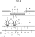
- FIG. 1 illustrates a cross-sectional view of a display device according to an exemplary embodiment
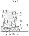
- FIG. 2 illustrates an enlarged view of the portion A in FIG. 1 .
- a display device may include a substrate 110.
- the substrate 110 may have flexibility.
- a buffer layer 111 may be disposed on the substrate 110.
- the buffer layer 111 may be omitted.
- the buffer layer 111 may include an inorganic material such as a silicon oxide, a silicon nitride, or the like.
- the buffer layer 111 may be provided as a single layer or a multilayer.
- the buffer layer 111 may planarize one surface of the substrate 110 or may help prevent dispersion of an impurity that causes deterioration of a characteristic of a semiconductor layer 154, which will be described later, and may help prevent permeation of moisture and the like.
- the semiconductor layer 154 of the transistor Tr may be disposed on the buffer layer 111.
- the semiconductor layer 154 may include a channel region 152, and a source region 153 and a drain region 155 that are disposed at opposite sides of the channel region 152 and doped with an impurity.
- the semiconductor layer 154 may include a polysilicon or an oxide semiconductor.
- the oxide semiconductor may include, e.g., an oxide that is based on titanium (Ti), hafnium (Hf), zirconium (Zr), aluminum (Al), tantalum (Ta), germanium (Ge), zinc (Zn), gallium (Ga), tin (Sn), or indium (In), or a complex oxide thereof.
- a light blocking electrode may be disposed between the substrate 110 and the semiconductor layer 154.
- the light blocking electrode may help prevent characteristic deterioration of the semiconductor layer 154 and minimize a leakage current of the transistor Tr by preventing external light from reaching the semiconductor layer 154.
- a gate insulation layer 141 may be disposed on the semiconductor layer 154 and the buffer layer 111.
- the gate insulating layer 141 may wholly or entirely overlap the substrate 110.
- the gate insulating layer 141 may include tetraethoxysilane (TEOS) and a silicon oxide or a silicon nitride.
- TEOS tetraethoxysilane
- the gate insulating layer 141 may be provided as a single layer or a multilayer.
- a gate conductor that includes a gate electrode 124 of the transistor Tr may be disposed on the gate insulation layer 141.
- the gate electrode 124 may overlap with the channel region 152 of the semiconductor layer 154.
- the gate conductor may include a metal such as molybdenum (Mo), copper (Cu), aluminum (Al), silver (Ag), chromium (Cr), tantalum (Ta), titanium (Ti), or the like, or a metal alloy.
- Mo molybdenum
- Cu copper
- Al aluminum
- Ag silver
- Cr chromium
- Ta tantalum
- Ti titanium
- the gate conductor may be provided as a single layer or a multilayer.
- An interlayer insulation layer 160 may be disposed on the gate electrode 124.
- the interlayer insulation layer 160 may include tetraethoxysilane (TEOS), a silicon oxide, or a silicon nitride.
- TEOS tetraethoxysilane
- the interlayer insulation layer 160 may be provided as a single layer or a multilayer formed by stacking the single layers.
- a data conductor that includes a source electrode 173 and a drain electrode 175 of the transistor Tr, data lines, a driving voltage line, or the like may be disposed on the interlayer insulation layer 160.
- the source electrode 173 and the drain electrode 175 may be respectively connected to the source region 153 and the drain region 155 of the semiconductor layer 154 through contact holes 63 and 65 in the interlayer insulation layer 160 and the gate insulating layer 141.
- a first spacer 161 and a second spacer 163 may be provided in each of the contact holes 63 and 65.
- the first spacer 161 and the second spacer 163 may be disposed between the source electrode 173 and the interlayer insulation layer 160 and between the drain electrode 175 and the interlayer insulation layer 160.
- the first spacer 161 and the second spacer 163 may be sequentially stacked with reference to an interior surface of the interlayer insulation layer 160 (e.g., the first spacer 161 may be between the second spacer 163 and the interlayer insulation layer 160).
- the first spacer 161 may directly contact the interlayer insulation layer 160 and the interior surface of the gate insulation layer 141.
- the first spacer 161 may have a shape that surrounds or conforms to the interlayer insulation layer 160 and the interior surface of the gate insulation layer 141 where the contact holes 63 and 65 are formed.
- the first spacer 161 may surround or be conformally on an internal circumferential surface of the contact holes 63 and 65.
- the first spacer 161 may include a vertical portion (first portion) that is formed in the shape of a piece of macaroni (e.g., in a hollow cylindrical or conical shape) that extends in a second direction D2, and a lower end portion 161a (second portion) that extends in a first direction Di from a lower end of the vertical portion.
- the lower end portion 161a of the first spacer 161 may directly contact one side of the semiconductor layer 154.
- the lower end portion 161a of the first spacer 161 may directly contact one side of the source region 153 or one side of the drain region 155.
- the second spacer 163 may have a shape that surrounds an external circumferential surface of the source electrode 173 or the drain electrode 175.
- the second spacer 163 may directly contact the source electrode 173 or the drain electrode 175 while directly contacting the first spacer 161.
- the second spacer 163 may have a shape of a piece of macaroni or a pipe (e.g., a hollow cylindrical or conical shape) that extends in the second direction D2.
- the source electrode 173 and the drain electrode 175 may directly contact the semiconductor layer 154 by penetrating the second spacer 163 and the first spacer 161.
- each of the source electrode 173 and the drain electrode 175 may be connected to the source region 153 and the drain region 155 of the semiconductor layer 154 by penetrating the lower end portion 161a of the first spacer 161.
- the second spacer 163 may overlap the source region 153 or the drain region 155.
- the lower end portion 161a of the first spacer 161 may be disposed between a bottom surface of the second spacer 163 and the source region 153 or between the bottom surface of the second spacer 163 and the drain region 155.
- the second spacer 163 may not directly contact the semiconductor layer 154.
- One side of the lower end portion 161a of the first spacer 161 and one side of the second spacer 163 may substantially form the same plane (e.g., an inner side or surface of the lower end portion 161a of the first spacer 161 and an inner side or surface of the second spacer 163 may be aligned or concentric).
- the one side of the lower end portion 161a of the first spacer 161 and the one side of the second spacer 163 that form the same plane may contact the source electrode 173 or the drain electrode 175.
- an upper surface of the first spacer 161, an upper surface of the second spacer 163, and an upper surface of the interlayer insulation layer 160 may substantially form the same plane (e.g. may be coplanar).
- a part of the source electrode 173 and the drain electrode 175 may be disposed on the upper surface of the first spacer 161, the upper surface of the second spacer 163, and the upper surface of the interlayer insulation layer 160 that form the same plane.
- the first spacer 161 and the second spacer 163 may have a shape of which a width is gradually reduced toward the substrate 110.
- the width of the source electrode 173 and the width of the drain electrode 175, which are disposed in the interior side of the second spacer 163, may be gradually reduced toward the substrate 110.
- the first spacer 161 may include an oxide, e.g., may include a silicon oxide.
- the second spacer 163 may include a nitride, e.g., may include a silicon nitride.
- the second spacer 163 may include the same material as the interlayer insulation layer 160, e.g., may include the same material as a layer that is disposed topmost in the interlayer insulation layer 160 that is formed of a plurality of layers.
- a thickness ti of the first spacer 161 may be smaller than a thickness t2 of the second spacer 163.
- the second spacer 163 may be thicker than the first spacer 161.
- a thickness ratio of the first spacer 161 and the second spacer 163 may be 1:1 to 1:20.
- Such a thickness ratio may be determined by an etching ratio between materials that respectively form the first spacer 161 and the second spacer 163.
- a material that forms the first spacer 161 and a material that forms the second spacer 163 may have an etching ratio of 1:1 to 1:3.
- the source region 153 that contacts the first spacer 161 and the source electrode 173, or the drain region 155 that contacts the first spacer 161 and the drain electrode 175, may have step-shaped first sides 155a and 155b.
- the semiconductor layer 154 may be partially etched during a process for forming the interlayer insulation layer 160 and the gate insulating layer 141, and may be partially etched during a process for forming the first spacer 161 and the second spacer 163.
- the semiconductor layer 154 which has been etched two times as described above, e.g., one side of the drain region 155 or one side of the source region 153, may have the step-shaped first sides 155a and 155b as shown in FIG. 2 .
- a surface that is neither flat not stepped as shown in FIG. 2 may be provided.
- the data conductor may include a metal such as aluminum (Al), copper (Cu), silver (Ag), gold (Au), platinum (Pt), palladium (Pd), nickel (Ni), molybdenum (Mo), tungsten (W), titanium (Ti), chromium (Cr), tantalum (Ta), or the like, or a metal alloy.
- the data conductor may be provided as a single layer or a multilayer (e.g., Ti/Al/Ti, Mo/Al/Mo, Mo/Cu/Mo).
- the gate electrode 124, the source electrode 173, and the drain electrode 175 form the transistor Tr together with the semiconductor layer 154.
- the transistor shown in the drawing may be a driving transistor in a pixel of the light emitting display device.
- the gate electrode 124 may be higher than the semiconductor layer 154 in the transistor, and the transistor Tr may be called a top-gate type of transistor.
- the transistor may be a bottom-gate transistor in which a gate electrode is disposed below a semiconductor layer.
- a driving thin film transistor of the pixel may be provided.
- signal lines and organic light emitting elements included in pixels may be formed with various suitable structures.
- a suitable number of thin film transistors, of capacitors, or wires maybe included.
- a planarization layer 180 may be disposed on the interlayer insulation layer 160 and the data conductor.
- the planarization layer 180 may remove a height difference and planarize a surface to improve light emission efficiency of a light emitting element that will be formed thereon.
- the planarization layer 180 may cover the transistor Tr.
- the planarization layer 180 may include, e.g., an organic insulation material.
- the organic insulation material may include, e.g., polyimide, polyamide, polyacrylate, polyphenylene ether, polyphenylene sulfide, unsaturated polyester, epoxy resin, phenol resin, or the like.
- a pixel electrode 191 may be disposed on the planarization layer 180.
- the pixel electrode 191 may be connected to the drain electrode 175 of the transistor Tr through a contact hole 81 formed in the planarization layer 180.
- the pixel electrode 191 may include a reflective conducting material or a semi-transmissive conducting material.
- the pixel electrode 191 may include, e.g., at least one of transparent conductive materials such as indium tin oxide (ITO), indium zinc oxide (IZO), and the like, and metals such as lithium (Li), calcium (Ca), aluminum (Al), silver (Ag), magnesium (Mg), and gold (Au).
- transparent conductive materials such as indium tin oxide (ITO), indium zinc oxide (IZO), and the like
- metals such as lithium (Li), calcium (Ca), aluminum (Al), silver (Ag), magnesium (Mg), and gold (Au).
- a pixel defining layer 360 may be disposed on the planarization layer 180 and the pixel electrode 191.
- the pixel defining layer 360 may have an opening 91 that partially overlaps the pixel electrode 191.
- the opening 91 of the pixel defining layer 360 may limit or define an area that corresponds to a pixel.
- the pixel defining layer 360 may include, e.g., an organic insulation material such as polyimide, polyacrylate, polyamide, and the like, or a silica-based inorganic material.
- An emission layer 370 may be disposed on the pixel electrode 191.
- the emission layer 370 includes an emission area, and may additionally include at least one of a hole injection area, a hole transport area, an electron injection area, and an electron transport area.
- the emission layer 370 may be made of an organic material that uniquely emits light of a primary color, such as red, green, and blue, or may have a structure in which a plurality of organic materials, each emitting light of a different color, are stacked.
- a common electrode 270 that transmits a common voltage may be disposed on the emission layer 370.
- the common electrode 270 may include, e.g., a transparent conductive material such as indium tin oxide (ITO), indium zinc oxide (IZO), or the like.
- the common electrode 270 may have light transmittance by thinly laminating a metal such as calcium (Ca), barium (Ba), magnesium (Mg), aluminum (Al), silver (Ag), and the like.
- a pixel electrode 191, an emission layer 370, and a common electrode 270 of each pixel form a light emission element, which is a light emitting diode (LED).
- the pixel electrode 191 may be an anode, which is a hole injection electrode
- the common electrode 270 may be a cathode, which is an electron injection electrode.
- the pixel electrode 191 may be a cathode and the common electrode 270 may be an anode.
- Holes and electrons are respectively injected into the emission layer 370 from the pixel electrode 191 and the common electrode 270, and light may be emitted when excitons being combinations of the injected holes and electrons shift from an excited state to a ground state.
- the display device may be one of a front emission type, a bottom emission type, and a dual display type depending on a light emission direction of the light emitting diode (LED).
- LED light emitting diode
- a thin film encapsulation layer may be disposed on the common electrode 270.
- the thin film encapsulation layer may include a plurality of inorganic layers, or may have a structure in which inorganic layers and organic layers are alternately stacked. Moisture permeation into the light emitting diode can thereby be prevented.
- the contact hole where the source electrode or the drain electrode is disposed may have a considerably small size due to the first spacer and the second spacer.
- the contact hole may have a diameter of about 1.5 ⁇ m or less in order to provide a high-resolution display device.
- a contact hole may be formed through an exposure process, and the first spacer and the second spacer, each having a predetermined thickness, may be disposed in the contact hole to thereby reduce the size of the contact hole almost by two times as a deposition thickness of each of the first and second spacers. Accordingly, a high-resolution display device may be provided.
- the first spacer may serve as an etch stopper that prevents the interlayer insulation layer from being excessively etched or a thin semiconductor layer from being lost while the first spacer and the second spacer are etched.
- a display device having improved reliability may be provided.
- FIG. 3 and FIG. 4 illustrate cross-sectional views of display devices respectively according to exemplary variations of the display device of FIG. 1 .
- description of components similar to those described in the above-described embodiments may be omitted.
- an interlayer insulation layer 160 may include a first interlayer insulation layer 160a and a second interlayer insulation layer 160b.
- the interlayer insulation layer 160 may be provided as a double-stacked layer.
- the interlayer insulation layer 160 may be provided as a multi-interlayer insulation layer including more than two layers.
- the first interlayer insulation layer 160a may be disposed on a gate electrode 124 and a gate insulating layer 141.
- the first interlayer insulation layer 160a may be provided as a single layer including tetraethoxysilane (TEOS), a silicon oxide, or a silicon nitride, or a multilayer of the single layers.
- TEOS tetraethoxysilane
- silicon oxide silicon oxide
- silicon nitride silicon nitride
- the second interlayer insulation layer 160b may be disposed between the first interlayer insulation layer 160a and a planarization layer 180.
- the second interlayer insulation layer 160b may include a high-k material, e.g., zirconium oxide (ZrO x ) or hafnium oxide (HfO x ).
- the second interlayer insulation layer 160b may help prevent the interlayer insulation layer 160 from being excessively etched while a first spacer 161 and a second spacer 163 are formed.
- the second interlayer insulation layer 160b may serve as an etch stopper.
- An upper surface of the first spacer 161, an upper surface of the second spacer 163, and an upper surface of the second interlayer insulation layer 160b may substantially form the same plane.
- a source electrode 173 and a drain electrode 175 may be disposed on the upper surface of the first spacer 161, the upper surface of the second spacer 163, and the upper surface of the second interlayer insulation layer 160b that form the same plane.
- a first spacer 161 and a second spacer 163 may be respectively provided in contact holes 63 and 65 according to the present exemplary variation.
- the first spacer 161 and the second spacer 163 may be respectively provided between a source electrode 173 and an interlayer insulation layer 160 and between a drain electrode 175 and the interlayer insulation layer 160 in the contact holes 63 and 65.
- the first spacer 161 and the second spacer 163 may be sequentially stacked with reference to an interior surface of the interlayer insulation layer 160.
- the first spacer 161 may have a shape of a cup.
- the first spacer 161 may include a pipe-shaped vertical portion that surrounds or is conformally on an inside circumferential surface of each of the contact holes 63 and 65, and a lower end 161a that contacts one side of the semiconductor layer 154.
- the lower end 161a of the spacer 161 may have a closed shape.
- An upper surface of the lower end 161a of the first spacer 161 and the source electrode 173, and the upper surface of the lower end 161a of the first spacer 161 and the drain electrode 175, may contact each other.
- the source electrode 173 and the drain electrode 175 may be electrically connected with the semiconductor layer 154 through the first spacer 161 rather than directly contacting the semiconductor layer 154.
- the first spacer 161 may include a material that may be electrically connected with the semiconductor layer 154.
- the first spacer 161 may include a material that can carry out ohmic contact, e.g., titanium (Ti), molybdenum (Mo), ITO, IZO, or GZO.
- the first spacer 161 may include one of materials included in the source electrode 173 and the drain electrode 175. In this case, the first spacer 161 may be formed during a process for forming the source electrode 173 and the drain electrode 175.
- an end of the first spacer 161 and an end of the source electrode 173 may be aligned. In an implementation, the end of the first spacer 171 and an end of the drain electrode 175 may be aligned.
- the first spacer 161 and a data conductor are formed through the same process, the first spacer 161 and the data conductor may include the same edges.
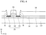
- FIG. 5 , FIG. 6 , FIG. 7 , and FIG. 8 are cross-sectional views of the manufacturing method of the display device. A detailed description of the same components as those of the above-described components may be omitted.
- a buffer layer 111 may be formed on a substrate 110.
- a semiconductor layer 154 that includes a channel region 152, and a source region 153 and a drain region 155 that are disposed at opposite sides of the channel region 152, may be formed on the buffer layer 111.
- a gate insulation material layer 141i that overlaps the entire surface of the substrate 110 may be formed on the semiconductor layer 154 and the buffer layer 111.
- a gate electrode 124 that overlaps the channel region 152 may be formed on the gate insulation material layer 141i.
- An interlayer insulation material layer 160i that overlaps the entire surface of the substrate 110 may be formed on the gate electrode 124 and the gate insulation material layer 141i.
- an interlayer insulation layer 160 and a gate insulation layer 141 may be formed.
- the contact hole 63 may expose the source region 153 and the contact hole 65 may expose the drain region 155.
- the interlayer insulation layer 160 and the gate insulation layer 141i may be formed by etching the gate insulation material layer 141i and the interlayer insulation material layer 160i.
- a first spacer material layer 161i and a second spacer material layer 163i may be formed all over (e.g., completely covering) the substrate 110.
- a first spacer 161 and a second spacer 163 may be formed by etching the first spacer material layer 161i and the second spacer material layer 163i.
- the first spacer 161 and the second spacer 163 may be formed by anisotropically etching the first spacer material layer 161i and the second spacer material layer 163i.
- the first spacer material layer 161i and the second spacer material layer 163i on the interlayer insulation layer 160 may be etched until the interlayer insulation layer 160 is exposed.
- the first spacer material layer 161i and the second spacer material layer 163i may be etched until the source region 153 and the drain region 155 of the semiconductor layer 154 are exposed.
- etching rates of the second spacer material 163i and the first spacer material layer 161i may be different from each other.
- an etching ratio between the second spacer material layer 163i and the first spacer material layer 161i may be 1:1 to 3:1.
- a degree of etching of the second spacer material layer 163i may be greater than a degree of etching of the first spacer material layer 161i.
- a thickness of the second spacer material layer 163i and a thickness of the first spacer material layer 161i may be determined.
- the second spacer material layer 163i may be thicker than the first spacer material layer 161i, e.g., a thickness ratio of the second spacer material layer 163i and the first spacer material layer 161i may be 1:1 to 20:1.
- the second spacer material layer 163i and the first spacer material layer 161i may include different materials, and the first spacer material layer 161i and the interlayer insulation layer 160 may include different materials.
- the first spacer material layer 161i and the second spacer material layer 163i may include different materials, the first spacer material layer 161i and the second spacer material layer 163i may have different etching rates, and thus the first spacer material layer 161i may serve as an etch stopper during a process for etching the second spacer material layer 163i.
- the interlayer insulation layer 160 may serve as an etch stopper during a process for etching the second spacer material layer 163i.
- Each layer may serve as an etch stopper during an etching process, and the interlayer insulation layer 160 or the semiconductor layer 154 can be prevented from being damaged.
- an etching selection ratio between the first spacer material layer 161i and the interlayer insulation layer 160 may be increased during a process for etching the first spacer material layer 161i. Accordingly, the spacers may be formed while minimizing damage to the interlayer insulation layer 160.
- the first spacer 161 when the first spacer 161 includes a material that can carry out ohmic contact, as shown in FIG. 4 , the first spacer material layer 161i may be etched during a process for forming the source electrode 173 and the drain electrode 175 and thus the first spacer 161 may be formed.
- the size of a pixel may become smaller as the structure has increased resolution.
- there may be a limit in a design rule due to a limit in equipment specifications and photolithography process capability.
- contact holes where the source electrode and the drain electrode are respectively disposed may be reduced to a considerably small size by the first spacer and the second spacer.
- the contact holes may be provided by using the exposure process, and the first spacer and the second spacer, each having a predetermined thickness, may be disposed in the contact holes such that the size of each of the contact holes may be reduced by almost two times (e.g., half the original size) as a deposition thickness of the first spacer and the second spacer. Accordingly, a high resolution display device can be provided.
- embodiments of the invention can provide a display device, comprising: a semiconductor layer over a substrate; a gate insulation layer and an interlayer insulation layer that overlap the semiconductor layer; contact holes that penetrate the gate insulation layer and the interlayer insulation layer; a source electrode and a drain electrode that are electrically connected with the semiconductor layer through corresponding contact holes; a light emitting diode that is connected with the drain electrode; and a first spacer and a second spacer between the source electrode and the interlayer insulation layer and a first spacer and a second spacer between the drain electrode and the interlayer insulation layer in the corresponding contact holes.
- Embodiments of the invention can provide a display device comprising a semiconductor layer over a substrate; a gate insulation layer and an interlayer insulation layer that overlap the semiconductor layer; first and second contact holes that penetrate the gate insulation layer and the interlayer insulation layer; a source electrode electrically connected with the semiconductor layer through the first contact hole and a drain electrode connected with the semiconductor layer through the second contact hole; a light emitting diode that is connected with the drain electrode; and a first spacer and a second spacer between the source electrode and the interlayer insulation layer in the first contact hole, and a first spacer and a second spacer between the drain electrode and the interlayer insulation layer in the second contact hole.
- the first spacer corresponding to the source electrode may be disposed in the contact hole for the source electrode such that the first spacer is between the corresponding second spacer and the interlayer insulation layer.
- the first spacer corresponding to the drain electrode may be disposed in the contact hole for the drain electrode such that the first spacer is between the corresponding second spacer and the interlayer insulation layer.
- the first spacers may each include: a first portion (vertical portion) extending along an inside circumferential surface of the corresponding contact hole; and a second portion (lower end) that is connected with the first portion and contacts the semiconductor layer.
- the source electrode and/or the drain electrode may penetrate the second portion of the corresponding first spacer.
- the source electrode may contact an inside surface of the corresponding second spacer and an inside surface of the second portion of the corresponding first spacer.
- the drain electrode may contact an inside surface of the corresponding second spacer and an inside surface of the second portion of the corresponding first spacer.
- a surface facing away from the substrate (upper surface) of the second portion of the first spacer corresponding to the source electrode may contact the source electrode.
- a surface facing away from the substrate of the second portion (upper surface) of the first spacer corresponding to the drain electrode may contacts the drain electrode.
- the embodiments may provide a display device that includes small-sized contact holes.
- a display device having small-sized contact holes may be provided. Accordingly, a high resolution display device may be provided. In addition, damage to the semiconductor layer and the interlayer insulation layer may be prevented, thereby improving reliability of the display device.
- the first spacer may serve as an etch stopper that can prevent the interlayer insulation layer from being excessively etched or a thin semiconductor layer from being lost during an etching process of the second spacer and the first spacer. Accordingly, a display device having more improved reliability can be provided.
Landscapes
- Engineering & Computer Science (AREA)
- Microelectronics & Electronic Packaging (AREA)
- Physics & Mathematics (AREA)
- Optics & Photonics (AREA)
- Manufacturing & Machinery (AREA)
- Geometry (AREA)
- Thin Film Transistor (AREA)
- Electroluminescent Light Sources (AREA)
- Devices For Indicating Variable Information By Combining Individual Elements (AREA)
- Electrodes Of Semiconductors (AREA)
Abstract
Description
- Embodiments relates to a display device and a method for manufacturing the same.
- A light emitting element is an element that emits light when an exciton formed by coupling holes injected from an anode and electrons injected from a cathode electrode with each other in the organic emission layer is stabilized.
- The light emitting element has various merits such as a wide viewing angle, a high response speed, a slim thickness, and low power consumption, and thus is widely applied to various electric and electronic devices such as a television, a monitor, a mobile phone, and the like.
- The above information disclosed in this Background section is only for enhancement of understanding of the background of the invention and therefore it may contain information that does not form the prior art that is already known in this country to a person of ordinary skill in the art.
- The embodiments may be realized by providing a display device including a semiconductor layer on a substrate; a gate insulation layer and an interlayer insulation layer that overlap the semiconductor layer; contact holes that penetrate the gate insulation layer and the interlayer insulation layer; a source electrode and a drain electrode that are electrically connected with the semiconductor layer through the contact holes; a light emitting diode that is connected with the drain electrode; and first spacers and second spacers between the source electrode and the interlayer insulation layer and between the drain electrode and the interlayer insulation layer in the contact holes.
- The first spacers and the second spacers may be sequentially disposed with reference to the interlayer insulation layer in the contact holes such that the first spacers are between the second spacers and the interlayer insulation layer.
- The first spacers may each include a vertical portion extending along an inside circumferential surface of each of the contact holes; and a lower end that is connected with the vertical portion and contacts the semiconductor layer.
- The source electrode or the drain electrode may penetrate the lower end.
- At least one of the source electrode and the drain electrode may contact an inside surface of the second spacers and an inside surface of the lower end of the first spacers.
- Upper surfaces of the lower ends of the first spacers may contact the source electrode or the drain electrode.
- The semiconductor layer may be electrically connected with the source electrode and the drain electrode through the first spacers.
- The first spacers may include titanium (Ti), molybdenum (Mo), ITO, IZO, or GZO.
- The source electrode and the drain electrode may include a same material as the first spacers.
- An end of one first spacer and an end of the source electrode may be aligned, or an end of another first spacer and an end of the drain electrode may be aligned.
- An upper surface of each first spacer, an upper surface of each second spacer, and an upper surface of the interlayer insulation layer may substantially form the same plane.
- One side of the semiconductor layer that overlaps at least one of the source electrode and the drain electrode may not be flat.
- One side of the semiconductor layer that overlaps at least one of the source electrode and the drain electrode may have a stepped shape.
- A thickness of the first spacers may be thinner than a thickness of the second spacers.
- An etching ratio between a material that forms the first spacers and a material that forms the second spacers maybe 1:1 to 1:3.
- The interlayer insulation layer may include zirconium oxide.
- The embodiments may be realized by providing a method for manufacturing a display device, the method including forming a semiconductor layer on a substrate; forming a gate insulation layer and an interlayer insulation layer that overlap the semiconductor layer; forming a contact hole that penetrates the gate insulation layer and the interlayer insulation layer; forming a first spacer material layer and a second spacer material layer on the substrate; exposing the interlayer insulation layer by etching the first spacer material layer and the second spacer material layer; forming a source electrode and a drain electrode on the interlayer insulation layer; and forming a light emitting element that is connected with the drain electrode.
- The method may further include forming first spacers by anisotropically etching the first spacer material layer; and forming second spacers by anisotropically etching the second spacer material layer.
- The semiconductor layer may be partially exposed while the first spacer material layer and the second spacer material layer are etched.
- An etching ratio between a material that forms the first spacer material layer and a material that forms the second spacer material layer may be 1:1 to 1:3.
- According to an aspect of the invention, there is provided a display device as set out in claim 1. Preferred features of this aspect are set out in claims 2 to 15.
- Features will be apparent to those of skill in the art by describing in detail exemplary embodiments with reference to the attached drawings in which:
-
FIG. 1 illustrates a cross-sectional view of a display device according to an exemplary embodiment. -
FIG. 2 illustrates an enlarged view of the portion A inFIG. 1 . -
FIG. 3 andFIG. 4 illustrate cross-sectional views of a display device according to an exemplary variation of the exemplary embodiment ofFIG. 1 . -
FIG. 5 ,FIG. 6 ,FIG. 7 , andFIG. 8 illustrate cross-sectional views of stages in a method for manufacturing a display device. - Example embodiments will now be described more fully hereinafter with reference to the accompanying drawings; however, they may be embodied in different forms and should not be construed as limited to the embodiments set forth herein. Rather, these embodiments are provided so that this disclosure will be thorough and complete, and will fully convey exemplary implementations to those skilled in the art.
- In the drawing figures, the dimensions of layers and regions may be exaggerated for clarity of illustration. In addition, it will also be understood that when a layer is referred to as being "between" two layers, it can be the only layer between the two layers, or one or more intervening layers may also be present. Like reference numerals refer to like elements throughout.
- It will be understood that when an element such as a layer, film, region, or substrate is referred to as being "on" another element, it can be directly on the other element or intervening elements may also be present. In contrast, when an element is referred to as being "directly on" another element, there are no intervening elements present. Further, throughout the specification, the word "on" means positioning on or below the object portion, but does not essentially mean positioning on the upper side of the object portion based on a gravitational direction.
- In addition, unless explicitly described to the contrary, the word "comprise" and variations such as "includes," "including," "comprises" or "comprising" will be understood to imply the inclusion of stated elements but not the exclusion of any other elements. The term "or" is not an exclusive term.
- In this specification, the phrase "on a plane" means viewing a target portion from the top, and the phrase "on a cross-section" means viewing a cross-section formed by vertically cutting a target portion from the side.
- Hereinafter, a display device according to an exemplary embodiment will be described with reference to
FIG. 1 andFIG. 2 .FIG. 1 illustrates a cross-sectional view of a display device according to an exemplary embodiment, andFIG. 2 illustrates an enlarged view of the portion A inFIG. 1 . - A display device according to an exemplary embodiment may include a
substrate 110. Thesubstrate 110 may have flexibility. - A
buffer layer 111 may be disposed on thesubstrate 110. In an implementation, thebuffer layer 111 may be omitted. Thebuffer layer 111 may include an inorganic material such as a silicon oxide, a silicon nitride, or the like. Thebuffer layer 111 may be provided as a single layer or a multilayer. - The
buffer layer 111 may planarize one surface of thesubstrate 110 or may help prevent dispersion of an impurity that causes deterioration of a characteristic of asemiconductor layer 154, which will be described later, and may help prevent permeation of moisture and the like. - The
semiconductor layer 154 of the transistor Tr may be disposed on thebuffer layer 111. Thesemiconductor layer 154 may include achannel region 152, and asource region 153 and adrain region 155 that are disposed at opposite sides of thechannel region 152 and doped with an impurity. - The
semiconductor layer 154 may include a polysilicon or an oxide semiconductor. The oxide semiconductor may include, e.g., an oxide that is based on titanium (Ti), hafnium (Hf), zirconium (Zr), aluminum (Al), tantalum (Ta), germanium (Ge), zinc (Zn), gallium (Ga), tin (Sn), or indium (In), or a complex oxide thereof. - In an implementation, a light blocking electrode may be disposed between the
substrate 110 and thesemiconductor layer 154. The light blocking electrode may help prevent characteristic deterioration of thesemiconductor layer 154 and minimize a leakage current of the transistor Tr by preventing external light from reaching thesemiconductor layer 154. - A
gate insulation layer 141 may be disposed on thesemiconductor layer 154 and thebuffer layer 111. Thegate insulating layer 141 may wholly or entirely overlap thesubstrate 110. - The
gate insulating layer 141 may include tetraethoxysilane (TEOS) and a silicon oxide or a silicon nitride. Thegate insulating layer 141 may be provided as a single layer or a multilayer. - A gate conductor that includes a
gate electrode 124 of the transistor Tr may be disposed on thegate insulation layer 141. Thegate electrode 124 may overlap with thechannel region 152 of thesemiconductor layer 154. - The gate conductor may include a metal such as molybdenum (Mo), copper (Cu), aluminum (Al), silver (Ag), chromium (Cr), tantalum (Ta), titanium (Ti), or the like, or a metal alloy. The gate conductor may be provided as a single layer or a multilayer.
- An
interlayer insulation layer 160 may be disposed on thegate electrode 124. Theinterlayer insulation layer 160 may include tetraethoxysilane (TEOS), a silicon oxide, or a silicon nitride. Theinterlayer insulation layer 160 may be provided as a single layer or a multilayer formed by stacking the single layers. - A data conductor that includes a
source electrode 173 and adrain electrode 175 of the transistor Tr, data lines, a driving voltage line, or the like may be disposed on theinterlayer insulation layer 160. - The
source electrode 173 and thedrain electrode 175 may be respectively connected to thesource region 153 and thedrain region 155 of thesemiconductor layer 154 through contact holes 63 and 65 in theinterlayer insulation layer 160 and thegate insulating layer 141. - A
first spacer 161 and asecond spacer 163 may be provided in each of the contact holes 63 and 65. In the contact holes 63 and 65, thefirst spacer 161 and thesecond spacer 163 may be disposed between thesource electrode 173 and theinterlayer insulation layer 160 and between thedrain electrode 175 and theinterlayer insulation layer 160. Thefirst spacer 161 and thesecond spacer 163 may be sequentially stacked with reference to an interior surface of the interlayer insulation layer 160 (e.g., thefirst spacer 161 may be between thesecond spacer 163 and the interlayer insulation layer 160). - The
first spacer 161 may directly contact theinterlayer insulation layer 160 and the interior surface of thegate insulation layer 141. Thefirst spacer 161 may have a shape that surrounds or conforms to theinterlayer insulation layer 160 and the interior surface of thegate insulation layer 141 where the contact holes 63 and 65 are formed. For example, thefirst spacer 161 may surround or be conformally on an internal circumferential surface of the contact holes 63 and 65. - The
first spacer 161 may include a vertical portion (first portion) that is formed in the shape of a piece of macaroni (e.g., in a hollow cylindrical or conical shape) that extends in a second direction D2, and alower end portion 161a (second portion) that extends in a first direction Di from a lower end of the vertical portion. Thelower end portion 161a of thefirst spacer 161 may directly contact one side of thesemiconductor layer 154. Thelower end portion 161a of thefirst spacer 161 may directly contact one side of thesource region 153 or one side of thedrain region 155. - The
second spacer 163 may have a shape that surrounds an external circumferential surface of thesource electrode 173 or thedrain electrode 175. Thesecond spacer 163 may directly contact thesource electrode 173 or thedrain electrode 175 while directly contacting thefirst spacer 161. Thesecond spacer 163 may have a shape of a piece of macaroni or a pipe (e.g., a hollow cylindrical or conical shape) that extends in the second direction D2. Thesource electrode 173 and thedrain electrode 175 may directly contact thesemiconductor layer 154 by penetrating thesecond spacer 163 and thefirst spacer 161. For example, each of thesource electrode 173 and thedrain electrode 175 may be connected to thesource region 153 and thedrain region 155 of thesemiconductor layer 154 by penetrating thelower end portion 161a of thefirst spacer 161. - The
second spacer 163 may overlap thesource region 153 or thedrain region 155. Thelower end portion 161a of thefirst spacer 161 may be disposed between a bottom surface of thesecond spacer 163 and thesource region 153 or between the bottom surface of thesecond spacer 163 and thedrain region 155. Thesecond spacer 163 may not directly contact thesemiconductor layer 154. - One side of the
lower end portion 161a of thefirst spacer 161 and one side of thesecond spacer 163 may substantially form the same plane (e.g., an inner side or surface of thelower end portion 161a of thefirst spacer 161 and an inner side or surface of thesecond spacer 163 may be aligned or concentric). The one side of thelower end portion 161a of thefirst spacer 161 and the one side of thesecond spacer 163 that form the same plane may contact thesource electrode 173 or thedrain electrode 175. - In an implementation, an upper surface of the
first spacer 161, an upper surface of thesecond spacer 163, and an upper surface of theinterlayer insulation layer 160 may substantially form the same plane (e.g. may be coplanar). A part of thesource electrode 173 and thedrain electrode 175 may be disposed on the upper surface of thefirst spacer 161, the upper surface of thesecond spacer 163, and the upper surface of theinterlayer insulation layer 160 that form the same plane. - The
first spacer 161 and thesecond spacer 163 may have a shape of which a width is gradually reduced toward thesubstrate 110. For example, the width of thesource electrode 173 and the width of thedrain electrode 175, which are disposed in the interior side of thesecond spacer 163, may be gradually reduced toward thesubstrate 110. - In an implementation, the
first spacer 161 may include an oxide, e.g., may include a silicon oxide. Thesecond spacer 163 may include a nitride, e.g., may include a silicon nitride. In an implementation, thesecond spacer 163 may include the same material as theinterlayer insulation layer 160, e.g., may include the same material as a layer that is disposed topmost in theinterlayer insulation layer 160 that is formed of a plurality of layers. - A thickness ti of the
first spacer 161 may be smaller than a thickness t2 of thesecond spacer 163. Thesecond spacer 163 may be thicker than thefirst spacer 161. For example, a thickness ratio of thefirst spacer 161 and thesecond spacer 163 may be 1:1 to 1:20. Such a thickness ratio may be determined by an etching ratio between materials that respectively form thefirst spacer 161 and thesecond spacer 163. For example, a material that forms thefirst spacer 161 and a material that forms thesecond spacer 163 may have an etching ratio of 1:1 to 1:3. - In an implementation, the
source region 153 that contacts thefirst spacer 161 and thesource electrode 173, or thedrain region 155 that contacts thefirst spacer 161 and thedrain electrode 175, may have step-shapedfirst sides - The
semiconductor layer 154 may be partially etched during a process for forming theinterlayer insulation layer 160 and thegate insulating layer 141, and may be partially etched during a process for forming thefirst spacer 161 and thesecond spacer 163. In an implementation, thesemiconductor layer 154, which has been etched two times as described above, e.g., one side of thedrain region 155 or one side of thesource region 153, may have the step-shapedfirst sides FIG. 2 . In an implementation, when thesemiconductor layer 154 has a very thin thickness or a degree of etching of thesemiconductor layer 154 during a process is considerably small, a surface that is neither flat not stepped as shown inFIG. 2 may be provided. - The data conductor may include a metal such as aluminum (Al), copper (Cu), silver (Ag), gold (Au), platinum (Pt), palladium (Pd), nickel (Ni), molybdenum (Mo), tungsten (W), titanium (Ti), chromium (Cr), tantalum (Ta), or the like, or a metal alloy. The data conductor may be provided as a single layer or a multilayer (e.g., Ti/Al/Ti, Mo/Al/Mo, Mo/Cu/Mo).
- The
gate electrode 124, thesource electrode 173, and thedrain electrode 175 form the transistor Tr together with thesemiconductor layer 154. The transistor shown in the drawing may be a driving transistor in a pixel of the light emitting display device. In an implementation, thegate electrode 124 may be higher than thesemiconductor layer 154 in the transistor, and the transistor Tr may be called a top-gate type of transistor. In an implementation, the transistor may be a bottom-gate transistor in which a gate electrode is disposed below a semiconductor layer. - In an implementation, a driving thin film transistor of the pixel may be provided. In an implementation, signal lines and organic light emitting elements included in pixels may be formed with various suitable structures. In an implementation, a suitable number of thin film transistors, of capacitors, or wires maybe included.
- A
planarization layer 180 may be disposed on theinterlayer insulation layer 160 and the data conductor. Theplanarization layer 180 may remove a height difference and planarize a surface to improve light emission efficiency of a light emitting element that will be formed thereon. Theplanarization layer 180 may cover the transistor Tr. - The
planarization layer 180 may include, e.g., an organic insulation material. In an implementation, the organic insulation material may include, e.g., polyimide, polyamide, polyacrylate, polyphenylene ether, polyphenylene sulfide, unsaturated polyester, epoxy resin, phenol resin, or the like. - A
pixel electrode 191 may be disposed on theplanarization layer 180. Thepixel electrode 191 may be connected to thedrain electrode 175 of the transistor Tr through acontact hole 81 formed in theplanarization layer 180. - The
pixel electrode 191 may include a reflective conducting material or a semi-transmissive conducting material. In an implementation, thepixel electrode 191 may include, e.g., at least one of transparent conductive materials such as indium tin oxide (ITO), indium zinc oxide (IZO), and the like, and metals such as lithium (Li), calcium (Ca), aluminum (Al), silver (Ag), magnesium (Mg), and gold (Au). - A
pixel defining layer 360 may be disposed on theplanarization layer 180 and thepixel electrode 191. Thepixel defining layer 360 may have anopening 91 that partially overlaps thepixel electrode 191. Theopening 91 of thepixel defining layer 360 may limit or define an area that corresponds to a pixel. - In an implementation, the
pixel defining layer 360 may include, e.g., an organic insulation material such as polyimide, polyacrylate, polyamide, and the like, or a silica-based inorganic material. - An
emission layer 370 may be disposed on thepixel electrode 191. Theemission layer 370 includes an emission area, and may additionally include at least one of a hole injection area, a hole transport area, an electron injection area, and an electron transport area. - The
emission layer 370 may be made of an organic material that uniquely emits light of a primary color, such as red, green, and blue, or may have a structure in which a plurality of organic materials, each emitting light of a different color, are stacked. - A
common electrode 270 that transmits a common voltage may be disposed on theemission layer 370. Thecommon electrode 270 may include, e.g., a transparent conductive material such as indium tin oxide (ITO), indium zinc oxide (IZO), or the like. In an implementation, thecommon electrode 270 may have light transmittance by thinly laminating a metal such as calcium (Ca), barium (Ba), magnesium (Mg), aluminum (Al), silver (Ag), and the like. - A
pixel electrode 191, anemission layer 370, and acommon electrode 270 of each pixel form a light emission element, which is a light emitting diode (LED). Thepixel electrode 191 may be an anode, which is a hole injection electrode, and thecommon electrode 270 may be a cathode, which is an electron injection electrode. In an implementation, thepixel electrode 191 may be a cathode and thecommon electrode 270 may be an anode. Holes and electrons are respectively injected into theemission layer 370 from thepixel electrode 191 and thecommon electrode 270, and light may be emitted when excitons being combinations of the injected holes and electrons shift from an excited state to a ground state. - The display device may be one of a front emission type, a bottom emission type, and a dual display type depending on a light emission direction of the light emitting diode (LED).
- In an implementation, a thin film encapsulation layer may be disposed on the
common electrode 270. The thin film encapsulation layer may include a plurality of inorganic layers, or may have a structure in which inorganic layers and organic layers are alternately stacked. Moisture permeation into the light emitting diode can thereby be prevented. - According to the above-stated exemplary embodiment, the contact hole where the source electrode or the drain electrode is disposed may have a considerably small size due to the first spacer and the second spacer. The contact hole may have a diameter of about 1.5 µm or less in order to provide a high-resolution display device. However, there may be a limit in manufacturing a small-sized contact hole by using an exposure process. For example, a contact hole may be formed through an exposure process, and the first spacer and the second spacer, each having a predetermined thickness, may be disposed in the contact hole to thereby reduce the size of the contact hole almost by two times as a deposition thickness of each of the first and second spacers. Accordingly, a high-resolution display device may be provided.
- In addition, the first spacer may serve as an etch stopper that prevents the interlayer insulation layer from being excessively etched or a thin semiconductor layer from being lost while the first spacer and the second spacer are etched. Thus, a display device having improved reliability may be provided.
- Hereinafter, a display device according to an exemplary variation will be described with reference to
FIG. 3 andFIG. 4 .FIG. 3 andFIG. 4 illustrate cross-sectional views of display devices respectively according to exemplary variations of the display device ofFIG. 1 . Hereinafter, description of components similar to those described in the above-described embodiments may be omitted. - First, referring to
FIG. 3 , aninterlayer insulation layer 160 according to the present exemplary variation may include a firstinterlayer insulation layer 160a and a secondinterlayer insulation layer 160b. In an implementation, as illustrated inFIG. 3 , theinterlayer insulation layer 160 may be provided as a double-stacked layer. In an implementation, theinterlayer insulation layer 160 may be provided as a multi-interlayer insulation layer including more than two layers. - The first
interlayer insulation layer 160a may be disposed on agate electrode 124 and agate insulating layer 141. In an implementation, the firstinterlayer insulation layer 160a may be provided as a single layer including tetraethoxysilane (TEOS), a silicon oxide, or a silicon nitride, or a multilayer of the single layers. - The second
interlayer insulation layer 160b may be disposed between the firstinterlayer insulation layer 160a and aplanarization layer 180. In an implementation, the secondinterlayer insulation layer 160b may include a high-k material, e.g., zirconium oxide (ZrOx) or hafnium oxide (HfOx). - The second
interlayer insulation layer 160b may help prevent theinterlayer insulation layer 160 from being excessively etched while afirst spacer 161 and asecond spacer 163 are formed. The secondinterlayer insulation layer 160b may serve as an etch stopper. - An upper surface of the
first spacer 161, an upper surface of thesecond spacer 163, and an upper surface of the secondinterlayer insulation layer 160b may substantially form the same plane. Asource electrode 173 and adrain electrode 175 may be disposed on the upper surface of thefirst spacer 161, the upper surface of thesecond spacer 163, and the upper surface of the secondinterlayer insulation layer 160b that form the same plane. - Next, referring to
FIG. 4 , afirst spacer 161 and asecond spacer 163 may be respectively provided in contact holes 63 and 65 according to the present exemplary variation. Thefirst spacer 161 and thesecond spacer 163 may be respectively provided between asource electrode 173 and aninterlayer insulation layer 160 and between adrain electrode 175 and theinterlayer insulation layer 160 in the contact holes 63 and 65. Thefirst spacer 161 and thesecond spacer 163 may be sequentially stacked with reference to an interior surface of theinterlayer insulation layer 160. - The
first spacer 161 may have a shape of a cup. Thefirst spacer 161 may include a pipe-shaped vertical portion that surrounds or is conformally on an inside circumferential surface of each of the contact holes 63 and 65, and alower end 161a that contacts one side of thesemiconductor layer 154. In the present exemplary variation, thelower end 161a of thespacer 161 may have a closed shape. - An upper surface of the
lower end 161a of thefirst spacer 161 and thesource electrode 173, and the upper surface of thelower end 161a of thefirst spacer 161 and thedrain electrode 175, may contact each other. For example, thesource electrode 173 and thedrain electrode 175 may be electrically connected with thesemiconductor layer 154 through thefirst spacer 161 rather than directly contacting thesemiconductor layer 154. - The
first spacer 161 may include a material that may be electrically connected with thesemiconductor layer 154. In an implementation, thefirst spacer 161 may include a material that can carry out ohmic contact, e.g., titanium (Ti), molybdenum (Mo), ITO, IZO, or GZO. - In an implementation, the
first spacer 161 may include one of materials included in thesource electrode 173 and thedrain electrode 175. In this case, thefirst spacer 161 may be formed during a process for forming thesource electrode 173 and thedrain electrode 175. - In an implementation, an end of the
first spacer 161 and an end of thesource electrode 173 may be aligned. In an implementation, the end of the first spacer 171 and an end of thedrain electrode 175 may be aligned. When thefirst spacer 161 and a data conductor are formed through the same process, thefirst spacer 161 and the data conductor may include the same edges. - Hereinafter, a method for manufacturing a display device according to an exemplary embodiment will be described with reference to
FIG. 5 to FIG. 8 .FIG. 5 ,FIG. 6 ,FIG. 7 , andFIG. 8 are cross-sectional views of the manufacturing method of the display device. A detailed description of the same components as those of the above-described components may be omitted. - First, as shown in
FIG. 5 , abuffer layer 111 may be formed on asubstrate 110. Asemiconductor layer 154 that includes achannel region 152, and asource region 153 and adrain region 155 that are disposed at opposite sides of thechannel region 152, may be formed on thebuffer layer 111. A gateinsulation material layer 141i that overlaps the entire surface of thesubstrate 110 may be formed on thesemiconductor layer 154 and thebuffer layer 111. Agate electrode 124 that overlaps thechannel region 152 may be formed on the gateinsulation material layer 141i. An interlayerinsulation material layer 160i that overlaps the entire surface of thesubstrate 110 may be formed on thegate electrode 124 and the gateinsulation material layer 141i. - Next, as shown in
FIG. 6 , aninterlayer insulation layer 160 and a gate insulation layer 141 (that include acontact hole 63 and a contact hole 65) may be formed. Thecontact hole 63 may expose thesource region 153 and thecontact hole 65 may expose thedrain region 155. Theinterlayer insulation layer 160 and thegate insulation layer 141i may be formed by etching the gateinsulation material layer 141i and the interlayerinsulation material layer 160i. - Next, as shown in
FIG. 7 , a firstspacer material layer 161i and a second spacer material layer 163i may be formed all over (e.g., completely covering) thesubstrate 110. - Next, as shown in
FIG. 8 , afirst spacer 161 and asecond spacer 163 may be formed by etching the firstspacer material layer 161i and the second spacer material layer 163i. - The
first spacer 161 and thesecond spacer 163 may be formed by anisotropically etching the firstspacer material layer 161i and the second spacer material layer 163i. The firstspacer material layer 161i and the second spacer material layer 163i on theinterlayer insulation layer 160 may be etched until theinterlayer insulation layer 160 is exposed. Simultaneously, the firstspacer material layer 161i and the second spacer material layer 163i may be etched until thesource region 153 and thedrain region 155 of thesemiconductor layer 154 are exposed. - During such an etching process, etching rates of the second spacer material 163i and the first
spacer material layer 161i may be different from each other. For example, an etching ratio between the second spacer material layer 163i and the firstspacer material layer 161i may be 1:1 to 3:1. A degree of etching of the second spacer material layer 163i may be greater than a degree of etching of the firstspacer material layer 161i. - Depending on the etching ratio, a thickness of the second spacer material layer 163i and a thickness of the first
spacer material layer 161i may be determined. The second spacer material layer 163i may be thicker than the firstspacer material layer 161i, e.g., a thickness ratio of the second spacer material layer 163i and the firstspacer material layer 161i may be 1:1 to 20:1. - In an implementation, the second spacer material layer 163i and the first
spacer material layer 161i may include different materials, and the firstspacer material layer 161i and theinterlayer insulation layer 160 may include different materials. - The first
spacer material layer 161i and the second spacer material layer 163i may include different materials, the firstspacer material layer 161i and the second spacer material layer 163i may have different etching rates, and thus the firstspacer material layer 161i may serve as an etch stopper during a process for etching the second spacer material layer 163i. In an implementation, theinterlayer insulation layer 160 may serve as an etch stopper during a process for etching the second spacer material layer 163i. - Each layer may serve as an etch stopper during an etching process, and the
interlayer insulation layer 160 or thesemiconductor layer 154 can be prevented from being damaged. - In an implementation, when the interlayer insulation layer includes zirconium oxide, as shown in
FIG. 3 , an etching selection ratio between the firstspacer material layer 161i and theinterlayer insulation layer 160 may be increased during a process for etching the firstspacer material layer 161i. Accordingly, the spacers may be formed while minimizing damage to theinterlayer insulation layer 160. - In an implementation, when the
first spacer 161 includes a material that can carry out ohmic contact, as shown inFIG. 4 , the firstspacer material layer 161i may be etched during a process for forming thesource electrode 173 and thedrain electrode 175 and thus thefirst spacer 161 may be formed. - By way of summation and review, the size of a pixel may become smaller as the structure has increased resolution. For example, there may be a limit in a design rule due to a limit in equipment specifications and photolithography process capability.
- When the display device is manufactured through the above-stated exemplary embodiments, contact holes where the source electrode and the drain electrode are respectively disposed may be reduced to a considerably small size by the first spacer and the second spacer. According to the exemplary embodiment, the contact holes may be provided by using the exposure process, and the first spacer and the second spacer, each having a predetermined thickness, may be disposed in the contact holes such that the size of each of the contact holes may be reduced by almost two times (e.g., half the original size) as a deposition thickness of the first spacer and the second spacer. Accordingly, a high resolution display device can be provided.
- As discussed, embodiments of the invention can provide a display device, comprising: a semiconductor layer over a substrate; a gate insulation layer and an interlayer insulation layer that overlap the semiconductor layer; contact holes that penetrate the gate insulation layer and the interlayer insulation layer; a source electrode and a drain electrode that are electrically connected with the semiconductor layer through corresponding contact holes; a light emitting diode that is connected with the drain electrode; and a first spacer and a second spacer between the source electrode and the interlayer insulation layer and a first spacer and a second spacer between the drain electrode and the interlayer insulation layer in the corresponding contact holes.
- Embodiments of the invention can provide a display device comprising a semiconductor layer over a substrate; a gate insulation layer and an interlayer insulation layer that overlap the semiconductor layer; first and second contact holes that penetrate the gate insulation layer and the interlayer insulation layer; a source electrode electrically connected with the semiconductor layer through the first contact hole and a drain electrode connected with the semiconductor layer through the second contact hole; a light emitting diode that is connected with the drain electrode; and a first spacer and a second spacer between the source electrode and the interlayer insulation layer in the first contact hole, and a first spacer and a second spacer between the drain electrode and the interlayer insulation layer in the second contact hole.
- The first spacer corresponding to the source electrode may be disposed in the contact hole for the source electrode such that the first spacer is between the corresponding second spacer and the interlayer insulation layer. The first spacer corresponding to the drain electrode may be disposed in the contact hole for the drain electrode such that the first spacer is between the corresponding second spacer and the interlayer insulation layer.
- The first spacers (i.e. those corresponding to the source electrode and those corresponding to the drain electrode) may each include: a first portion (vertical portion) extending along an inside circumferential surface of the corresponding contact hole; and a second portion (lower end) that is connected with the first portion and contacts the semiconductor layer.
- The source electrode and/or the drain electrode may penetrate the second portion of the corresponding first spacer.
- The source electrode may contact an inside surface of the corresponding second spacer and an inside surface of the second portion of the corresponding first spacer. The drain electrode may contact an inside surface of the corresponding second spacer and an inside surface of the second portion of the corresponding first spacer.
- A surface facing away from the substrate (upper surface) of the second portion of the first spacer corresponding to the source electrode may contact the source electrode. A surface facing away from the substrate of the second portion (upper surface) of the first spacer corresponding to the drain electrode may contacts the drain electrode.
- The embodiments may provide a display device that includes small-sized contact holes.
- According to the exemplary embodiments, a display device having small-sized contact holes may be provided. Accordingly, a high resolution display device may be provided. In addition, damage to the semiconductor layer and the interlayer insulation layer may be prevented, thereby improving reliability of the display device.
- In addition, the first spacer may serve as an etch stopper that can prevent the interlayer insulation layer from being excessively etched or a thin semiconductor layer from being lost during an etching process of the second spacer and the first spacer. Accordingly, a display device having more improved reliability can be provided.
- Example embodiments have been disclosed herein, and although specific terms are employed, they are used and are to be interpreted in a generic and descriptive sense only and not for purpose of limitation. In some instances, as would be apparent to one of ordinary skill in the art as of the filing of the present application, features, characteristics, and/or elements described in connection with a particular embodiment may be used singly or in combination with features, characteristics, and/or elements described in connection with other embodiments unless otherwise specifically indicated. Accordingly, it will be understood by those of skill in the art that various changes in form and details may be made without departing from the scope of the present invention as set forth in the following claims.
Claims (15)
- A display device, comprising:a semiconductor layer over a substrate;a gate insulation layer and an interlayer insulation layer that overlap the semiconductor layer;contact holes that penetrate the gate insulation layer and the interlayer insulation layer;a source electrode and a drain electrode that are electrically connected with the semiconductor layer through the contact holes;a light emitting diode that is connected with the drain electrode; andfirst spacers and second spacers between the source electrode and the interlayer insulation layer and between the drain electrode and the interlayer insulation layer in the contact holes.
- The display device as claimed in claim 1, wherein the first spacers and the second spacers are sequentially disposed with reference to the interlayer insulation layer in the contact holes such that the first spacers are between the second spacers and the interlayer insulation layer.
- The display device as claimed in claim 1 or 2, wherein the first spacers each include:a first portion extending along an inside circumferential surface of the corresponding contact hole; anda second portion that is connected with the first portion and contacts the semiconductor layer.
- The display device as claimed in claim 3, wherein the source electrode and/or the drain electrode penetrates the second portion of the corresponding first spacer.
- The display device as claimed in claim 3 or 4, wherein the source electrode contacts an inside surface of the corresponding second spacer and an inside surface of the second portion of the corresponding first spacer; and/or
wherein the drain electrode contacts an inside surface of the corresponding second spacer and an inside surface of the second portion of the corresponding first spacer. - The display device as claimed in claim 3, wherein a surface facing away from the substrate of the second portion of the first spacer corresponding to the source electrode contacts the source electrode; and/or
wherein a surface facing away from the substrate of the second portion of the first spacer corresponding to the drain electrode contacts the drain electrode. - The display device as claimed in claim 6, wherein the semiconductor layer is electrically connected with the source electrode and the drain electrode through the corresponding first spacers.
- The display device as claimed in claim 7, wherein the first spacers include titanium (Ti), molybdenum (Mo), ITO, IZO, or GZO.
- The display device as claimed in claim 8, wherein the source electrode and the drain electrode include a same material as the first spacers.
- The display device as claimed in any one of claims 7 to 9, wherein:an end of one first spacer and an end of the source electrode are aligned, oran end of another first spacer and an end of the drain electrode are aligned.
- The display device as claimed in any one of claims 1 to 10, wherein one side of the semiconductor layer that overlaps at least one of the source electrode and the drain electrode is not flat.
- The display device as claimed in claim 11, wherein one side of the semiconductor layer that overlaps at least one of the source electrode and the drain electrode has a stepped shape.
- The display device as claimed in any one of claims 1 to 12, wherein a thickness of the first spacers is thinner than a thickness of the second spacers.
- The display device as claimed in any one of claims 1 to 13, wherein an etching ratio between a material that forms the first spacers and a material that forms the second spacers is 1:1 to 1:3.
- The display device as claimed in any one of claims 1 to 14, wherein the interlayer insulation layer includes zirconium oxide.
Applications Claiming Priority (1)
| Application Number | Priority Date | Filing Date | Title |
|---|---|---|---|
| KR1020180027352A KR102560100B1 (en) | 2018-03-08 | 2018-03-08 | Display device and manufacturing method thereof |
Publications (2)
| Publication Number | Publication Date |
|---|---|
| EP3537481A1 true EP3537481A1 (en) | 2019-09-11 |
| EP3537481B1 EP3537481B1 (en) | 2024-08-07 |
Family
ID=65724312
Family Applications (1)
| Application Number | Title | Priority Date | Filing Date |
|---|---|---|---|
| EP19161402.3A Active EP3537481B1 (en) | 2018-03-08 | 2019-03-07 | Display device and manufacturing method thereof |
Country Status (5)
| Country | Link |
|---|---|
| US (1) | US11101336B2 (en) |
| EP (1) | EP3537481B1 (en) |
| JP (1) | JP7280716B2 (en) |
| KR (1) | KR102560100B1 (en) |
| CN (1) | CN110246847B (en) |
Cited By (1)
| Publication number | Priority date | Publication date | Assignee | Title |
|---|---|---|---|---|
| US11908874B2 (en) * | 2021-03-23 | 2024-02-20 | Samsung Display Co., Ltd. | Organic light emissive display having an insulating layer contacting a semiconductor layer through a contact hole |
Families Citing this family (5)
| Publication number | Priority date | Publication date | Assignee | Title |
|---|---|---|---|---|
| KR102608021B1 (en) | 2018-09-03 | 2023-12-01 | 삼성디스플레이 주식회사 | Electronic apparatus and method of manufacturing the same |
| JP2020136312A (en) * | 2019-02-13 | 2020-08-31 | 株式会社ジャパンディスプレイ | Semiconductor device and method for manufacturing semiconductor device |
| WO2021250782A1 (en) * | 2020-06-09 | 2021-12-16 | シャープ株式会社 | Display device and method for producing display device |
| JP2022016320A (en) * | 2020-07-09 | 2022-01-21 | 東レ株式会社 | Organic el display device and manufacturing method thereof |
| KR20230073403A (en) * | 2021-11-18 | 2023-05-26 | 삼성디스플레이 주식회사 | Display device and method for fabricating the saem |
Citations (2)
| Publication number | Priority date | Publication date | Assignee | Title |
|---|---|---|---|---|
| US20030227021A1 (en) * | 2002-06-07 | 2003-12-11 | Semiconductor Energy Laboratory Co., Ltd. | Light emitting device and manufacturing method thereof |
| US20060001091A1 (en) * | 2004-06-30 | 2006-01-05 | Tae-Seong Kim | Thin film transistor (TFT) and flat panel display including the TFT and their methods of manufacture |
Family Cites Families (26)
| Publication number | Priority date | Publication date | Assignee | Title |
|---|---|---|---|---|
| JP3587537B2 (en) * | 1992-12-09 | 2004-11-10 | 株式会社半導体エネルギー研究所 | Semiconductor device |
| JP3989761B2 (en) | 2002-04-09 | 2007-10-10 | 株式会社半導体エネルギー研究所 | Semiconductor display device |
| US7579771B2 (en) * | 2002-04-23 | 2009-08-25 | Semiconductor Energy Laboratory Co., Ltd. | Light emitting device and method of manufacturing the same |
| US7786496B2 (en) * | 2002-04-24 | 2010-08-31 | Semiconductor Energy Laboratory Co., Ltd. | Semiconductor device and method of manufacturing same |
| JP2003317971A (en) * | 2002-04-26 | 2003-11-07 | Semiconductor Energy Lab Co Ltd | Light emitting device and manufacturing method thereof |
| JP4401688B2 (en) | 2002-06-07 | 2010-01-20 | 株式会社半導体エネルギー研究所 | LIGHT EMITTING DEVICE, ITS MANUFACTURING METHOD, AND ELECTRONIC DEVICE |
| JP4216008B2 (en) * | 2002-06-27 | 2009-01-28 | 株式会社半導体エネルギー研究所 | LIGHT EMITTING DEVICE AND ITS MANUFACTURING METHOD, AND VIDEO CAMERA, DIGITAL CAMERA, GOGGLE TYPE DISPLAY, CAR NAVIGATION, PERSONAL COMPUTER, DVD PLAYER, ELECTRONIC GAME EQUIPMENT, OR PORTABLE INFORMATION TERMINAL HAVING THE LIGHT EMITTING DEVICE |
| JP4373086B2 (en) * | 2002-12-27 | 2009-11-25 | 株式会社半導体エネルギー研究所 | Light emitting device |
| US7948171B2 (en) * | 2005-02-18 | 2011-05-24 | Semiconductor Energy Laboratory Co., Ltd. | Light emitting device |
| JP5170964B2 (en) | 2005-02-18 | 2013-03-27 | 株式会社半導体エネルギー研究所 | Method for manufacturing light emitting device |
| US8149346B2 (en) * | 2005-10-14 | 2012-04-03 | Semiconductor Energy Laboratory Co., Ltd. | Display device and manufacturing method thereof |
| JP4946003B2 (en) * | 2005-10-26 | 2012-06-06 | セイコーエプソン株式会社 | Electro-optical device and method of manufacturing electro-optical device |
| JP2007165563A (en) * | 2005-12-13 | 2007-06-28 | Toshiba Matsushita Display Technology Co Ltd | Manufacturing method of substrate device |
| KR100752388B1 (en) * | 2006-11-01 | 2007-08-27 | 삼성에스디아이 주식회사 | Flat panel display and manufacturing method |
| KR100964227B1 (en) * | 2008-05-06 | 2010-06-17 | 삼성모바일디스플레이주식회사 | Thin film transistor array substrate for flat panel display, organic light emitting display device comprising same, and manufacturing method thereof |
| US8614131B2 (en) * | 2009-02-03 | 2013-12-24 | Taiwan Semiconductor Manufacturing Company, Ltd. | Self-aligned static random access memory (SRAM) on metal gate |
| KR101074803B1 (en) | 2009-11-24 | 2011-10-19 | 삼성모바일디스플레이주식회사 | Organic light emitting display apparatus and method of manufacturing thereof |
| TWI419324B (en) * | 2009-11-27 | 2013-12-11 | Univ Nat Chiao Tung | Semiconductor device having three-five-group channel and four-group source drain and manufacturing method thereof |
| KR101686095B1 (en) | 2010-04-21 | 2016-12-13 | 엘지디스플레이 주식회사 | Organic light emitting display device and method for fabricating the same |
| KR20120140474A (en) * | 2011-06-21 | 2012-12-31 | 삼성디스플레이 주식회사 | Organic light emitting display device and method for manufacturing the same |
| KR20140095797A (en) | 2013-01-25 | 2014-08-04 | 삼성디스플레이 주식회사 | Thin film transistor array panel and manufacturing method thereof |
| US10181573B2 (en) * | 2014-07-11 | 2019-01-15 | Lg Display Co., Ltd. | Organic light-emitting diode display device and method of fabricating the same |
| KR102246296B1 (en) | 2014-12-19 | 2021-04-30 | 삼성디스플레이 주식회사 | Display device |
| KR102481382B1 (en) | 2016-01-18 | 2022-12-27 | 삼성디스플레이 주식회사 | Thin film transistor substrate, liquid crystal display and manufacturing method thereof |
| JP6784522B2 (en) | 2016-06-30 | 2020-11-11 | 株式会社ジャパンディスプレイ | Display device |
| KR102618350B1 (en) | 2016-12-14 | 2023-12-28 | 삼성디스플레이 주식회사 | Display device |
-
2018
- 2018-03-08 KR KR1020180027352A patent/KR102560100B1/en active Active
-
2019
- 2019-01-29 US US16/260,293 patent/US11101336B2/en active Active
- 2019-03-01 JP JP2019037873A patent/JP7280716B2/en active Active
- 2019-03-07 EP EP19161402.3A patent/EP3537481B1/en active Active
- 2019-03-08 CN CN201910176154.9A patent/CN110246847B/en active Active
Patent Citations (2)
| Publication number | Priority date | Publication date | Assignee | Title |
|---|---|---|---|---|
| US20030227021A1 (en) * | 2002-06-07 | 2003-12-11 | Semiconductor Energy Laboratory Co., Ltd. | Light emitting device and manufacturing method thereof |
| US20060001091A1 (en) * | 2004-06-30 | 2006-01-05 | Tae-Seong Kim | Thin film transistor (TFT) and flat panel display including the TFT and their methods of manufacture |
Cited By (2)
| Publication number | Priority date | Publication date | Assignee | Title |
|---|---|---|---|---|
| US11908874B2 (en) * | 2021-03-23 | 2024-02-20 | Samsung Display Co., Ltd. | Organic light emissive display having an insulating layer contacting a semiconductor layer through a contact hole |
| US12266664B2 (en) | 2021-03-23 | 2025-04-01 | Samsung Display Co., Ltd. | Display device having an insulating layer contacting a semiconductor layer through a contact hole |
Also Published As
| Publication number | Publication date |
|---|---|
| KR102560100B1 (en) | 2023-07-26 |
| EP3537481B1 (en) | 2024-08-07 |
| CN110246847B (en) | 2024-12-03 |
| JP7280716B2 (en) | 2023-05-24 |
| KR20190107233A (en) | 2019-09-19 |
| CN110246847A (en) | 2019-09-17 |
| US11101336B2 (en) | 2021-08-24 |
| JP2019159321A (en) | 2019-09-19 |
| US20190280067A1 (en) | 2019-09-12 |
Similar Documents
| Publication | Publication Date | Title |
|---|---|---|
| EP3537481B1 (en) | Display device and manufacturing method thereof | |
| USRE50700E1 (en) | Organic light emitting display device and method of manufacturing an organic light emitting display device | |
| US10236309B2 (en) | Display device and manufacturing method thereof | |
| US9105864B2 (en) | Organic light-emitting display device and method of manufacturing the same | |
| US9281349B2 (en) | Organic light-emitting display device | |
| US8421084B2 (en) | Organic light emitting display and manufacturing method thereof | |
| US11018263B2 (en) | Display device and method of manufacturing the same | |
| US11296297B2 (en) | Display device having an inorganic layer covering an end of a first electrode | |
| US12414425B2 (en) | Display apparatus having a substrate hole | |
| US12144204B2 (en) | Display substrate including a common buffer layer | |
| US20180090620A1 (en) | Thin film transistor array panel and manufacturing method thereof | |
| CN115715118A (en) | display device | |
| US10431762B2 (en) | Display device and manufacturing method thereof | |
| US10468534B2 (en) | Transistor array panel and manufacturing method thereof | |
| JP6654997B2 (en) | Thin film transistor substrate | |
| US8227804B2 (en) | Organic light-emitting display device | |
| CN112186004A (en) | Display device | |
| US12563789B2 (en) | Thin film transistor and method for manufacturing the same | |
| US20240324293A1 (en) | Display apparatus | |
| US20240049510A1 (en) | Display device |
Legal Events
| Date | Code | Title | Description |
|---|---|---|---|
| PUAI | Public reference made under article 153(3) epc to a published international application that has entered the european phase |
Free format text: ORIGINAL CODE: 0009012 |
|
| STAA | Information on the status of an ep patent application or granted ep patent |
Free format text: STATUS: THE APPLICATION HAS BEEN PUBLISHED |
|
| AK | Designated contracting states |
Kind code of ref document: A1 Designated state(s): AL AT BE BG CH CY CZ DE DK EE ES FI FR GB GR HR HU IE IS IT LI LT LU LV MC MK MT NL NO PL PT RO RS SE SI SK SM TR |
|
| AX | Request for extension of the european patent |
Extension state: BA ME |
|
| STAA | Information on the status of an ep patent application or granted ep patent |
Free format text: STATUS: REQUEST FOR EXAMINATION WAS MADE |
|
| 17P | Request for examination filed |
Effective date: 20200311 |
|
| RBV | Designated contracting states (corrected) |
Designated state(s): AL AT BE BG CH CY CZ DE DK EE ES FI FR GB GR HR HU IE IS IT LI LT LU LV MC MK MT NL NO PL PT RO RS SE SI SK SM TR |
|
| STAA | Information on the status of an ep patent application or granted ep patent |
Free format text: STATUS: EXAMINATION IS IN PROGRESS |
|
| 17Q | First examination report despatched |
Effective date: 20200707 |
|
| P01 | Opt-out of the competence of the unified patent court (upc) registered |
Effective date: 20230516 |
|
| GRAP | Despatch of communication of intention to grant a patent |
Free format text: ORIGINAL CODE: EPIDOSNIGR1 |
|
| STAA | Information on the status of an ep patent application or granted ep patent |
Free format text: STATUS: GRANT OF PATENT IS INTENDED |
|
| RIC1 | Information provided on ipc code assigned before grant |
Ipc: H10K 59/12 20230101ALN20240426BHEP Ipc: H01L 27/12 20060101ALI20240426BHEP Ipc: H01L 29/786 20060101ALI20240426BHEP Ipc: H01L 29/45 20060101ALI20240426BHEP Ipc: H01L 29/417 20060101AFI20240426BHEP |
|
| INTG | Intention to grant announced |
Effective date: 20240529 |
|
| GRAS | Grant fee paid |
Free format text: ORIGINAL CODE: EPIDOSNIGR3 |
|
| GRAA | (expected) grant |
Free format text: ORIGINAL CODE: 0009210 |
|
| STAA | Information on the status of an ep patent application or granted ep patent |
Free format text: STATUS: THE PATENT HAS BEEN GRANTED |
|
| AK | Designated contracting states |
Kind code of ref document: B1 Designated state(s): AL AT BE BG CH CY CZ DE DK EE ES FI FR GB GR HR HU IE IS IT LI LT LU LV MC MK MT NL NO PL PT RO RS SE SI SK SM TR |
|
| REG | Reference to a national code |
Ref country code: GB Ref legal event code: FG4D |
|
| REG | Reference to a national code |
Ref country code: CH Ref legal event code: EP |
|
| REG | Reference to a national code |
Ref country code: IE Ref legal event code: FG4D |
|
| REG | Reference to a national code |
Ref country code: DE Ref legal event code: R096 Ref document number: 602019056432 Country of ref document: DE |
|
| REG | Reference to a national code |
Ref country code: DE Ref legal event code: R079 Ref document number: 602019056432 Country of ref document: DE Free format text: PREVIOUS MAIN CLASS: H01L0029417000 Ipc: H10D0064230000 |
|
| REG | Reference to a national code |
Ref country code: LT Ref legal event code: MG9D |
|
| REG | Reference to a national code |
Ref country code: NL Ref legal event code: MP Effective date: 20240807 |
|
| PG25 | Lapsed in a contracting state [announced via postgrant information from national office to epo] |
Ref country code: NO Free format text: LAPSE BECAUSE OF FAILURE TO SUBMIT A TRANSLATION OF THE DESCRIPTION OR TO PAY THE FEE WITHIN THE PRESCRIBED TIME-LIMIT Effective date: 20241107 |
|
| REG | Reference to a national code |
Ref country code: AT Ref legal event code: MK05 Ref document number: 1711943 Country of ref document: AT Kind code of ref document: T Effective date: 20240807 |
|
| PG25 | Lapsed in a contracting state [announced via postgrant information from national office to epo] |
Ref country code: NL Free format text: LAPSE BECAUSE OF FAILURE TO SUBMIT A TRANSLATION OF THE DESCRIPTION OR TO PAY THE FEE WITHIN THE PRESCRIBED TIME-LIMIT Effective date: 20240807 Ref country code: PT Free format text: LAPSE BECAUSE OF FAILURE TO SUBMIT A TRANSLATION OF THE DESCRIPTION OR TO PAY THE FEE WITHIN THE PRESCRIBED TIME-LIMIT Effective date: 20241209 Ref country code: FI Free format text: LAPSE BECAUSE OF FAILURE TO SUBMIT A TRANSLATION OF THE DESCRIPTION OR TO PAY THE FEE WITHIN THE PRESCRIBED TIME-LIMIT Effective date: 20240807 Ref country code: GR Free format text: LAPSE BECAUSE OF FAILURE TO SUBMIT A TRANSLATION OF THE DESCRIPTION OR TO PAY THE FEE WITHIN THE PRESCRIBED TIME-LIMIT Effective date: 20241108 Ref country code: PL Free format text: LAPSE BECAUSE OF FAILURE TO SUBMIT A TRANSLATION OF THE DESCRIPTION OR TO PAY THE FEE WITHIN THE PRESCRIBED TIME-LIMIT Effective date: 20240807 |
|
| PG25 | Lapsed in a contracting state [announced via postgrant information from national office to epo] |
Ref country code: BG Free format text: LAPSE BECAUSE OF FAILURE TO SUBMIT A TRANSLATION OF THE DESCRIPTION OR TO PAY THE FEE WITHIN THE PRESCRIBED TIME-LIMIT Effective date: 20240807 |
|
| PG25 | Lapsed in a contracting state [announced via postgrant information from national office to epo] |
Ref country code: LV Free format text: LAPSE BECAUSE OF FAILURE TO SUBMIT A TRANSLATION OF THE DESCRIPTION OR TO PAY THE FEE WITHIN THE PRESCRIBED TIME-LIMIT Effective date: 20240807 |
|
| PG25 | Lapsed in a contracting state [announced via postgrant information from national office to epo] |
Ref country code: AT Free format text: LAPSE BECAUSE OF FAILURE TO SUBMIT A TRANSLATION OF THE DESCRIPTION OR TO PAY THE FEE WITHIN THE PRESCRIBED TIME-LIMIT Effective date: 20240807 Ref country code: IS Free format text: LAPSE BECAUSE OF FAILURE TO SUBMIT A TRANSLATION OF THE DESCRIPTION OR TO PAY THE FEE WITHIN THE PRESCRIBED TIME-LIMIT Effective date: 20241207 |
|
| PG25 | Lapsed in a contracting state [announced via postgrant information from national office to epo] |
Ref country code: HR Free format text: LAPSE BECAUSE OF FAILURE TO SUBMIT A TRANSLATION OF THE DESCRIPTION OR TO PAY THE FEE WITHIN THE PRESCRIBED TIME-LIMIT Effective date: 20240807 |
|
| PG25 | Lapsed in a contracting state [announced via postgrant information from national office to epo] |
Ref country code: ES Free format text: LAPSE BECAUSE OF FAILURE TO SUBMIT A TRANSLATION OF THE DESCRIPTION OR TO PAY THE FEE WITHIN THE PRESCRIBED TIME-LIMIT Effective date: 20240807 Ref country code: RS Free format text: LAPSE BECAUSE OF FAILURE TO SUBMIT A TRANSLATION OF THE DESCRIPTION OR TO PAY THE FEE WITHIN THE PRESCRIBED TIME-LIMIT Effective date: 20241107 |
|
| PG25 | Lapsed in a contracting state [announced via postgrant information from national office to epo] |
Ref country code: RS Free format text: LAPSE BECAUSE OF FAILURE TO SUBMIT A TRANSLATION OF THE DESCRIPTION OR TO PAY THE FEE WITHIN THE PRESCRIBED TIME-LIMIT Effective date: 20241107 Ref country code: PT Free format text: LAPSE BECAUSE OF FAILURE TO SUBMIT A TRANSLATION OF THE DESCRIPTION OR TO PAY THE FEE WITHIN THE PRESCRIBED TIME-LIMIT Effective date: 20241209 Ref country code: PL Free format text: LAPSE BECAUSE OF FAILURE TO SUBMIT A TRANSLATION OF THE DESCRIPTION OR TO PAY THE FEE WITHIN THE PRESCRIBED TIME-LIMIT Effective date: 20240807 Ref country code: NO Free format text: LAPSE BECAUSE OF FAILURE TO SUBMIT A TRANSLATION OF THE DESCRIPTION OR TO PAY THE FEE WITHIN THE PRESCRIBED TIME-LIMIT Effective date: 20241107 Ref country code: NL Free format text: LAPSE BECAUSE OF FAILURE TO SUBMIT A TRANSLATION OF THE DESCRIPTION OR TO PAY THE FEE WITHIN THE PRESCRIBED TIME-LIMIT Effective date: 20240807 Ref country code: LV Free format text: LAPSE BECAUSE OF FAILURE TO SUBMIT A TRANSLATION OF THE DESCRIPTION OR TO PAY THE FEE WITHIN THE PRESCRIBED TIME-LIMIT Effective date: 20240807 Ref country code: IS Free format text: LAPSE BECAUSE OF FAILURE TO SUBMIT A TRANSLATION OF THE DESCRIPTION OR TO PAY THE FEE WITHIN THE PRESCRIBED TIME-LIMIT Effective date: 20241207 Ref country code: HR Free format text: LAPSE BECAUSE OF FAILURE TO SUBMIT A TRANSLATION OF THE DESCRIPTION OR TO PAY THE FEE WITHIN THE PRESCRIBED TIME-LIMIT Effective date: 20240807 Ref country code: GR Free format text: LAPSE BECAUSE OF FAILURE TO SUBMIT A TRANSLATION OF THE DESCRIPTION OR TO PAY THE FEE WITHIN THE PRESCRIBED TIME-LIMIT Effective date: 20241108 Ref country code: FI Free format text: LAPSE BECAUSE OF FAILURE TO SUBMIT A TRANSLATION OF THE DESCRIPTION OR TO PAY THE FEE WITHIN THE PRESCRIBED TIME-LIMIT Effective date: 20240807 Ref country code: ES Free format text: LAPSE BECAUSE OF FAILURE TO SUBMIT A TRANSLATION OF THE DESCRIPTION OR TO PAY THE FEE WITHIN THE PRESCRIBED TIME-LIMIT Effective date: 20240807 Ref country code: BG Free format text: LAPSE BECAUSE OF FAILURE TO SUBMIT A TRANSLATION OF THE DESCRIPTION OR TO PAY THE FEE WITHIN THE PRESCRIBED TIME-LIMIT Effective date: 20240807 Ref country code: AT Free format text: LAPSE BECAUSE OF FAILURE TO SUBMIT A TRANSLATION OF THE DESCRIPTION OR TO PAY THE FEE WITHIN THE PRESCRIBED TIME-LIMIT Effective date: 20240807 |
|
| PG25 | Lapsed in a contracting state [announced via postgrant information from national office to epo] |
Ref country code: RO Free format text: LAPSE BECAUSE OF FAILURE TO SUBMIT A TRANSLATION OF THE DESCRIPTION OR TO PAY THE FEE WITHIN THE PRESCRIBED TIME-LIMIT Effective date: 20240807 Ref country code: DK Free format text: LAPSE BECAUSE OF FAILURE TO SUBMIT A TRANSLATION OF THE DESCRIPTION OR TO PAY THE FEE WITHIN THE PRESCRIBED TIME-LIMIT Effective date: 20240807 Ref country code: SM Free format text: LAPSE BECAUSE OF FAILURE TO SUBMIT A TRANSLATION OF THE DESCRIPTION OR TO PAY THE FEE WITHIN THE PRESCRIBED TIME-LIMIT Effective date: 20240807 |
|
| PG25 | Lapsed in a contracting state [announced via postgrant information from national office to epo] |
Ref country code: EE Free format text: LAPSE BECAUSE OF FAILURE TO SUBMIT A TRANSLATION OF THE DESCRIPTION OR TO PAY THE FEE WITHIN THE PRESCRIBED TIME-LIMIT Effective date: 20240807 |
|
| PG25 | Lapsed in a contracting state [announced via postgrant information from national office to epo] |
Ref country code: CZ Free format text: LAPSE BECAUSE OF FAILURE TO SUBMIT A TRANSLATION OF THE DESCRIPTION OR TO PAY THE FEE WITHIN THE PRESCRIBED TIME-LIMIT Effective date: 20240807 |
|
| PG25 | Lapsed in a contracting state [announced via postgrant information from national office to epo] |
Ref country code: SK Free format text: LAPSE BECAUSE OF FAILURE TO SUBMIT A TRANSLATION OF THE DESCRIPTION OR TO PAY THE FEE WITHIN THE PRESCRIBED TIME-LIMIT Effective date: 20240807 |
|
| REG | Reference to a national code |
Ref country code: DE Ref legal event code: R097 Ref document number: 602019056432 Country of ref document: DE |
|
| PLBE | No opposition filed within time limit |
Free format text: ORIGINAL CODE: 0009261 |
|
| STAA | Information on the status of an ep patent application or granted ep patent |
Free format text: STATUS: NO OPPOSITION FILED WITHIN TIME LIMIT |
|
| 26N | No opposition filed |
Effective date: 20250508 |
|
| PG25 | Lapsed in a contracting state [announced via postgrant information from national office to epo] |
Ref country code: SE Free format text: LAPSE BECAUSE OF FAILURE TO SUBMIT A TRANSLATION OF THE DESCRIPTION OR TO PAY THE FEE WITHIN THE PRESCRIBED TIME-LIMIT Effective date: 20240807 |
|
| PG25 | Lapsed in a contracting state [announced via postgrant information from national office to epo] |
Ref country code: MC Free format text: LAPSE BECAUSE OF FAILURE TO SUBMIT A TRANSLATION OF THE DESCRIPTION OR TO PAY THE FEE WITHIN THE PRESCRIBED TIME-LIMIT Effective date: 20240807 |
|
| REG | Reference to a national code |
Ref country code: CH Ref legal event code: H13 Free format text: ST27 STATUS EVENT CODE: U-0-0-H10-H13 (AS PROVIDED BY THE NATIONAL OFFICE) Effective date: 20251023 |
|
| PG25 | Lapsed in a contracting state [announced via postgrant information from national office to epo] |
Ref country code: LU Free format text: LAPSE BECAUSE OF NON-PAYMENT OF DUE FEES Effective date: 20250307 |
|
| REG | Reference to a national code |
Ref country code: BE Ref legal event code: MM Effective date: 20250331 |
|
| PG25 | Lapsed in a contracting state [announced via postgrant information from national office to epo] |
Ref country code: BE Free format text: LAPSE BECAUSE OF NON-PAYMENT OF DUE FEES Effective date: 20250331 |
|
| PG25 | Lapsed in a contracting state [announced via postgrant information from national office to epo] |
Ref country code: CH Free format text: LAPSE BECAUSE OF NON-PAYMENT OF DUE FEES Effective date: 20250331 |
|
| PG25 | Lapsed in a contracting state [announced via postgrant information from national office to epo] |
Ref country code: IE Free format text: LAPSE BECAUSE OF NON-PAYMENT OF DUE FEES Effective date: 20250307 |
|
| PG25 | Lapsed in a contracting state [announced via postgrant information from national office to epo] |
Ref country code: IT Free format text: LAPSE BECAUSE OF FAILURE TO SUBMIT A TRANSLATION OF THE DESCRIPTION OR TO PAY THE FEE WITHIN THE PRESCRIBED TIME-LIMIT Effective date: 20240807 |
|
| PGFP | Annual fee paid to national office [announced via postgrant information from national office to epo] |
Ref country code: GB Payment date: 20260224 Year of fee payment: 8 |
|
| PGFP | Annual fee paid to national office [announced via postgrant information from national office to epo] |
Ref country code: DE Payment date: 20260220 Year of fee payment: 8 |
|
| PGFP | Annual fee paid to national office [announced via postgrant information from national office to epo] |
Ref country code: FR Payment date: 20260224 Year of fee payment: 8 |