EP3537470A1 - Electron microscope adapted to introduce an arbitrary aberration - Google Patents
Electron microscope adapted to introduce an arbitrary aberration Download PDFInfo
- Publication number
- EP3537470A1 EP3537470A1 EP19160394.3A EP19160394A EP3537470A1 EP 3537470 A1 EP3537470 A1 EP 3537470A1 EP 19160394 A EP19160394 A EP 19160394A EP 3537470 A1 EP3537470 A1 EP 3537470A1
- Authority
- EP
- European Patent Office
- Prior art keywords
- aberration
- electron microscope
- correction device
- image
- processing
- Prior art date
- Legal status (The legal status is an assumption and is not a legal conclusion. Google has not performed a legal analysis and makes no representation as to the accuracy of the status listed.)
- Granted
Links
Images



Classifications
-
- H—ELECTRICITY
- H01—ELECTRIC ELEMENTS
- H01J—ELECTRIC DISCHARGE TUBES OR DISCHARGE LAMPS
- H01J37/00—Discharge tubes with provision for introducing objects or material to be exposed to the discharge, e.g. for the purpose of examination or processing thereof
- H01J37/02—Details
- H01J37/04—Arrangements of electrodes and associated parts for generating or controlling the discharge, e.g. electron-optical arrangement or ion-optical arrangement
- H01J37/153—Electron-optical or ion-optical arrangements for the correction of image defects, e.g. stigmators
-
- H—ELECTRICITY
- H01—ELECTRIC ELEMENTS
- H01J—ELECTRIC DISCHARGE TUBES OR DISCHARGE LAMPS
- H01J37/00—Discharge tubes with provision for introducing objects or material to be exposed to the discharge, e.g. for the purpose of examination or processing thereof
- H01J37/02—Details
- H01J37/22—Optical, image processing or photographic arrangements associated with the tube
- H01J37/222—Image processing arrangements associated with the tube
-
- H—ELECTRICITY
- H01—ELECTRIC ELEMENTS
- H01J—ELECTRIC DISCHARGE TUBES OR DISCHARGE LAMPS
- H01J37/00—Discharge tubes with provision for introducing objects or material to be exposed to the discharge, e.g. for the purpose of examination or processing thereof
- H01J37/26—Electron or ion microscopes; Electron or ion diffraction tubes
- H01J37/261—Details
- H01J37/265—Controlling the tube; circuit arrangements adapted to a particular application not otherwise provided, e.g. bright-field-dark-field illumination
-
- H—ELECTRICITY
- H01—ELECTRIC ELEMENTS
- H01J—ELECTRIC DISCHARGE TUBES OR DISCHARGE LAMPS
- H01J2237/00—Discharge tubes exposing object to beam, e.g. for analysis treatment, etching, imaging
- H01J2237/153—Correcting image defects, e.g. stigmators
- H01J2237/1534—Aberrations
-
- H—ELECTRICITY
- H01—ELECTRIC ELEMENTS
- H01J—ELECTRIC DISCHARGE TUBES OR DISCHARGE LAMPS
- H01J2237/00—Discharge tubes exposing object to beam, e.g. for analysis treatment, etching, imaging
- H01J2237/22—Treatment of data
- H01J2237/221—Image processing
-
- H—ELECTRICITY
- H01—ELECTRIC ELEMENTS
- H01J—ELECTRIC DISCHARGE TUBES OR DISCHARGE LAMPS
- H01J2237/00—Discharge tubes exposing object to beam, e.g. for analysis treatment, etching, imaging
- H01J2237/26—Electron or ion microscopes
- H01J2237/28—Scanning microscopes
- H01J2237/2802—Transmission microscopes
-
- H—ELECTRICITY
- H01—ELECTRIC ELEMENTS
- H01J—ELECTRIC DISCHARGE TUBES OR DISCHARGE LAMPS
- H01J2237/00—Discharge tubes exposing object to beam, e.g. for analysis treatment, etching, imaging
- H01J2237/26—Electron or ion microscopes
- H01J2237/282—Determination of microscope properties
Definitions
- the present invention relates to an electron microscope.
- TEM transmission electron microscope
- STEM scanning transmission electron microscope
- the invention can provide an electron microscope with good operability.
- an electron microscope including:
- an electron microscope including:
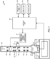
- FIG. 1 illustrates the configuration of an electron microscope 100 according to the first embodiment.
- the electron microscope 100 is a scanning transmission electron microscope (STEM) equipped with an optical system including an aberration correction device 30.
- a scanning transmission electron microscope image STEM image
- STEM image can be obtained by scanning a sample S with an electron probe (focused electron beam) and detecting electrons transmitted through the sample S.
- the electron microscope 100 includes an electron source 10, an optical system (a condenser lens 12, a scanning coil 13, an objective lens 14, an intermediate lens 18, a projection lens 20, an aberration correction device 30), a sample stage 16, a sample holder 17, STEM detectors 22a and 22b, an image capturing device 24, a control unit 40, an operation unit 50, a display unit 52, and a storage unit 54.
- the electron source 10 generates electrons.
- the electron source 10 is, for example, an electron gun that accelerates electrons emitted from a cathode with an anode and emits an electron beam.
- the condenser lens 12 focuses the electron beam emitted from the electron source 10.
- the condenser lens 12 may be configured of a plurality of electronic lenses.
- the condenser lens 12 and the objective lens 14 constitute an irradiation system of the electron microscope 100.
- the scanning coil 13 is a coil for deflecting the electron beam and scanning the sample S with an electron beam (electron probe) focused by the condenser lens 12 and the objective lens 14.
- the scanning coil 13 deflects the electron probe based on a scanning signal generated by a control device (not shown) of the electron microscope 100. As a result, it is possible to scan the sample S with the electron probe.
- the objective lens 14 is a lens for focusing the electron beam onto the sample S to form the electron probe. Further, the objective lens 14 forms an image with electrons transmitted through the sample S.
- the sample stage 16 supports the sample S held by the sample holder 17.
- the sample S can be positioned by the sample stage 16.
- the intermediate lens 18 and the projection lens 20 guide the electrons transmitted through the sample S to the STEM detectors 22a and 22b.
- the intermediate lens 18 and the projection lens 20 further enlarge the image formed by the objective lens 14 and form an image on the image capturing device 24.
- the objective lens 14, the intermediate lens 18, and the projection lens 20 constitute an image-forming system of the electron microscope 100.
- the bright-field STEM detector 22a detects electrons transmitted without being scattered and electrons scattered at a predetermined angle or less among electrons transmitted through the sample S.
- the bright-field STEM detector 22a is arranged on the optical axis, but this detector can be withdrawn from the optical axis when the image capturing device 24 is used.
- the dark-field STEM detector 22b detects electrons scattered at a specific angle by the sample S.
- the dark-field STEM detector 22b is an annular detector.
- the image capturing device 24 captures the image formed by the image-forming system.
- the image capturing device 24 is, for example, a digital camera such as a charge coupled device (CCD) camera.
- CCD charge coupled device
- the aberration correction device 30 is incorporated in the irradiation system of the electron microscope 100.
- the aberration correction device 30 is arranged at a stage behind the condenser lens 12.
- the aberration correction device 30 corrects the aberration of the irradiation system of the electron microscope 100.
- the aberration correction device 30 is a spherical aberration correction device that corrects a spherical aberration of the irradiation system by generating a negative spherical aberration and canceling a positive spherical aberration of the irradiation system.
- the electron beam emitted from the electron source 10 is focused by the condenser lens 12 and the objective lens 14 to form an electron probe which is radiated onto the sample S.
- the aberration of the electron beam radiated onto the sample S is corrected by the aberration correction device 30.
- the electron beam radiated onto the sample S is scanned on the sample S by the scanning coil 13.
- the electron beam transmitted through the sample S is guided to the STEM detectors 22a and 22b by the objective lens 14, the intermediate lens 18 and the projection lens 20, and detected by the STEM detectors 22a and 22b.
- the STEM detectors 22a and 22b send intensity signals (detection signals) of the detected electrons to a signal processing unit (not shown).
- the signal processing unit synchronizes the intensity signals (detection signals) of the electrons detected by the STEM detectors 22a and 22b with a scanning signal to form images and generates a bright-field STEM image and a dark-field STEM image.
- the image capturing device 24 can acquire a projection image (Ronchigram) of the sample that appears on the diffraction surface by focusing the electron beam near the sample S with the irradiation system. Information on the projection image (Ronchigram) acquired by the image capturing device 24 is sent to the control unit 40.
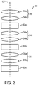
- FIG. 2 schematically illustrates the aberration correction device 30.
- the aberration correction device 30 has three stages of multipole elements 32a, 32b, and 32c. That is, the aberration correction device 30 is a three-stage three-fold-field type spherical aberration correction device.
- the aberration correction device 30 is configured to include three stages of multipole elements (first multipole element 32a, second multipole element 32b, and third multipole element 32c), a first transfer lens system 34, and a second transfer lens system 35.
- the first multipole element 32a generates a three-fold symmetric field.
- the three-fold symmetric field is a field where the field strength has three symmetries.
- the three-fold symmetric field generated by the first multipole element 32a is a three-fold symmetric electric field, a three-fold symmetric magnetic field, or a three-fold symmetric electromagnetic field.
- the first multipole element 32a is, for example, a twelve-pole element.
- the first multipole element 32a is not limited to a twelve-pole element as long as a three-fold symmetric field can be generated.
- the first multipole element 32a has a thickness along the optical axis OP.
- aberration different from the aberration occurring in a thin multipole element appears as a combination aberration.
- negative spherical aberration occurs as a combination aberration.
- this negative spherical aberration is used to correct the positive spherical aberration of the irradiation system.
- the configurations of the second multipole element 32b and the third multipole element 32c are the same as that of the first multipole element 32a. That is, each of the second multipole element 32b and the third multipole element 32c generates a three-fold symmetric field. In addition, the second multipole element 32b and the third multipole element 32c each have a thickness along the optical axis OP.
- the first transfer lens system 34 is disposed between the first multipole element 32a and the second multipole element 32b.
- the first transfer lens system 34 is configured of a pair of transfer lenses (a first transfer lens 34a and a second transfer lens 34b).
- a second transfer lens system 35 is disposed between the second multipole element 32b and the third multipole element 32c.
- the second transfer lens system 35 is configured of a pair of transfer lenses (a first transfer lens 35a and a second transfer lens 35b).
- a transfer lens system 36 is disposed between the condenser lens 12 and the first multipole element 32a.
- the transfer lens system 36 includes a pair of transfer lenses (a first transfer lens 36a and a second transfer lens 36b).
- the aberration correction device 30 is a three-stage three-fold-field type spherical aberration correction device, but the aberration correction device 30 is not limited to the three-stage three-fold-field type spherical aberration correction device, and various types of aberration correction devices can be used.
- the operation unit 50 acquires an operation signal corresponding to the operation by the user and performs processing of sending the operation signal to the control unit 40.
- the function of the operation unit 50 can be realized by, for example, a button, a key, a touch panel type display, a microphone or the like. By using the operation unit 50, it is possible to rotate an indicator 4 which will be described hereinbelow.
- the display unit 52 displays the image generated by the control unit 40, and the function thereof can be realized by a display such as a liquid crystal display (LCD).
- a display such as a liquid crystal display (LCD).
- LCD liquid crystal display
- GUI graphical user interface
- the storage unit 54 stores programs, data, and the like for the control unit 40 to perform various calculation processing and control processing.
- the storage unit 54 is also used as a work area of the control unit 40 and is also used for temporarily storing calculation results and the like executed by the control unit 40 according to various programs.
- the function of the storage unit 54 can be realized by a hard disk, a random access memory (RAM), or the like.
- the control unit 40 performs processing for controlling the aberration correction device.
- the processing of the control unit 40 will be described hereinbelow.
- the function of the control unit 40 can be realized by executing a program by various processors (central processing unit (CPU) etc.).
- FIGS. 3 and 4 illustrate a GUI for controlling the aberration correction device 30.
- an indicator 4 for designating the direction of aberration is displayed in superposition on an aberration pattern 2 showing the state of aberration.
- the aberration pattern 2 is a Ronchigram representing the state of aberration of the irradiation system.
- the aberration pattern 2 may be a previously acquired Ronchigram.
- the Ronchigram may be also constantly captured by the image capturing device 24, and the Ronchigram may be displayed on the display unit 52 in real time.
- the aberration pattern 2 is not limited to the Ronchigram as long as it is an image representing the state of aberration.
- a probe tableau method is known as a STEM aberration measurement method.
- a probe tableau method a plurality of STEM images is captured by changing the angle of electron beam irradiation on the sample surface, and aberration is measured based on a probe image obtained by deconvolution of the captured images. This probe image may be used as the aberration pattern 2.
- a phase map indicating the state of aberration may be used as the aberration pattern 2.
- the indicator 4 is an image for designating the direction of aberration.
- the indicator 4 has a shape corresponding to the type of aberration to be introduced.
- the indicator 4 may be displayed as an image having symmetry corresponding to the symmetry of the aberration.
- the shape of the indicator 4 is also changed.
- the indicator 4 is an image having three markers 6, the markers 6 being arranged on a circle at 120° intervals.
- the indicator 4 is an image having five markers 6, the markers 6 being arranged on a circle at 72° intervals.
- the shape of the indicator 4 is not particularly limited as long as the shape corresponds to the type of aberration.
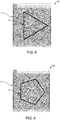
- FIG. 5 and FIG. 6 illustrate modified examples of the indicator 4.
- the indicator 4 may be an equilateral triangle. As a result, it is possible to easily grasp the direction of aberration having three-fold symmetry, and intuitively designate the direction of aberration.
- the indicator 4 may be a regular pentagon. As a result, it is possible to easily grasp the direction of aberration having five-fold symmetry, and intuitively designate the direction of aberration.
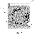
- FIG. 7 is a diagram for describing the operation of the indicator 4.
- the indicator 4 can be rotated using a pointing device such as a mouse (an example of the operation unit 50). Further, when the display unit 52 is a touch panel type display, the indicator 4 can be rotated by sliding a hand, a pen, or the like while touching the indicator 4 displayed on the display unit 52. By the rotation operation of the indicator 4, it is possible to designate the direction of aberration.
- the direction indicated by the indicator 4 after the rotation operation of the indicator 4 is the direction of the introduced aberration.
- the magnitude of the aberration is easy to understand by expressing it numerically. Therefore, the magnitude of the aberration is designated numerically. Instead of inputting numerical values, the magnitude of the aberration may be designated by wheel operation of a mouse or the like. Further, the magnitude of the aberration can be set in both the positive direction and the negative direction. Therefore, it is possible to intentionally introduce an aberration, and it is also possible to correct an aberration.
- FIG. 8 is a flowchart illustrating an example of processing of the control unit 40.
- a Ronchigram as an aberration pattern 2 showing the state of the aberration of the irradiation system is captured in advance, stored in the storage unit 54 and displayed on the display unit 52.
- control unit 40 receives information on the type of aberration to be introduced (S10).
- the control unit 40 receives the operation signal and acquires information on the type of aberration to be introduced.
- the control unit 40 Upon receiving the information on the type of aberration, the control unit 40 displays the indicator 4 on the display unit 52 in superposition on the aberration pattern 2 (Ronchigram) (S20). At this time, the control unit 40 causes the display unit 52 to display the indicator 4 having a shape corresponding to the type of aberration to be introduced, based on information on the type of aberration to be introduced.
- control unit 40 performs the processing of determining whether or not the direction of the aberration has been designated (S30).
- control unit 40 specifies the direction of the aberration from the indicator 4 having been subjected to the rotation operation and acquires the information of the direction of the aberration to be introduced (S40).
- the control unit 40 performs the processing of determining whether or not the magnitude of the aberration has been designated (S50).
- the control unit 40 acquires information on the magnitude of the inputted aberration (S60).
- the control unit 40 controls the aberration correction device 30 so that the designated type of aberration is introduced with the designated direction and magnitude, based on the acquired aberration direction information and aberration magnitude information (S70).
- the control unit 40 generates a control signal based on the acquired aberration type information, aberration direction information, and aberration magnitude information, and sends the control signal to the aberration correction power source controller 31.
- the aberration correction device 30 operates, and the designated type of aberration is introduced with the designated direction and magnitude.
- the electron microscope 100 has, for example, the following features.
- the electron microscope 100 includes the optical system including the aberration correction device 30, and the control unit 40 that controls the aberration correction device 30, the control unit 40 performing: processing for displaying, on the display unit 52, an indicator 4 for designating the direction of aberration in superposition on the aberration pattern 2 representing the state of aberration, processing for specifying the direction of aberration from the indicator 4 having been subjected to a rotation operation, and processing for controlling the aberration correction device 30 to cause the aberration correction device to introduce the aberration in the specified direction. Therefore, in the electron microscope 100, it is possible to intuitively perform the operation of designating the direction of the aberration to be introduced, and the operability is good.
- the control unit 40 performs processing of receiving information on the type of aberration to be introduced, and in the processing of displaying the indicator 4 on the display unit 52, the indicator 4 having the shape corresponding to the type of aberration is displayed on the display unit 52 based on the information of the type of aberration. Therefore, with the electron microscope 100, it is possible to intuitively perform the operation of designating the direction of the aberration to be introduced, and the operability is good.
- FIG. 9 is a diagram illustrating the configuration of an electron microscope 200 according to the second embodiment.
- members having functions similar to those of the members constituting the electron microscope 100 according to the first embodiment are denoted by the same reference numerals, and a detailed description thereof will be omitted.
- the aberration correction device 30 is incorporated in the irradiation system.
- the aberration correction device 30 is incorporated in the image capturing system.
- the aberration correction device 30 corrects the aberration of the imaging system.
- the electron beam emitted from the electron source 10 is focused by the condenser lens 12 and irradiated onto the sample S.
- the image of the electron beam transmitted through the sample S is formed by the objective lens 14, the intermediate lens 18 and the projection lens 20.
- the formed transmission electron microscope image (TEM image) is captured by the image capturing device 24.
- TEM image transmission electron microscope image
- a diffractogram tableau can be used as the aberration pattern 2.
- FIG. 10 illustrates a GUI for operating the aberration correction device 30.
- an indicator 4 for designating the direction of aberration is displayed on the diffractogram tableau serving as the aberration pattern 2 showing the state of aberration.
- the aberration pattern 2 is not limited to the diffractogram tableau as long as it is an image representing the state of aberration of the image-forming system.
- the electron microscope 200 similarly to the electron microscope 100, it is possible to intuitively perform the operation of designating the direction of the aberration to be introduced, and the operability is good.
- the indicator 4 has a shape corresponding to the type of aberration, but the shape of the indicator 4 is not limited as long as the direction of the aberration can be designated.
- the indicator 4 may be an arrow.
- the direction of the aberration can be designated by the arrow as the indicator 4. Even with such an indicator 4, an operation of designating the direction of the aberration to be introduced can be intuitively performed.
- the invention includes configurations that are substantially the same (for example in function and method) as the configurations described in the embodiments.
- the invention also includes configurations in which non-essential elements described in the embodiments are replaced by other elements.
- the invention further includes configurations obtained by adding known art to the configurations described in the embodiments.
Landscapes
- Chemical & Material Sciences (AREA)
- Analytical Chemistry (AREA)
- Engineering & Computer Science (AREA)
- Computer Vision & Pattern Recognition (AREA)
- Analysing Materials By The Use Of Radiation (AREA)
- Physics & Mathematics (AREA)
- Geometry (AREA)
- General Physics & Mathematics (AREA)
Abstract
Description
- The present invention relates to an electron microscope.
- In a transmission electron microscope (TEM) or a scanning transmission electron microscope (STEM), aberration correction is an important technique for acquiring a high-resolution image.
- The procedure of aberration correction in the transmission electron microscope is complicated. Therefore, in recent years, automation of aberration correction has been advanced. A technique for such automation of aberration correction is disclosed, for example, in
JP-A-2015-215970 - In aberration correction, the accuracy of aberration measurement becomes important. Conventionally, various aberration measurement methods have been suggested, but there are cases where aberration cannot be correctly measured, for example, when the aberration is small. For this reason, even when the user can recognize the aberration, where aberration correction is automated, it is impossible to correct the aberration. Further, in some cases, in order to cancel an arbitrary aberration, it is desirable to intentionally introduce another aberration. Thus, in some cases, the user may want to introduce an arbitrary aberration when performing aberration correction.
- In order for the user to introduce an aberration, it is necessary to designate the direction of the aberration, but in the conventional electron microscope, the operability of the operation for designating the direction of aberration is poor.
- The invention can provide an electron microscope with good operability.
- According to one aspect of the invention, there is provided an electron microscope including:
- an optical system including an aberration correction device; and
- a control unit that controls the aberration correction device,
- the control unit performing:
- processing for displaying, on a display unit, an image for designating a direction of aberration in superposition on an aberration pattern representing a state of aberration;
- processing for specifying the direction of aberration from the image that has been subjected to a rotation operation; and
- processing for controlling the aberration correction device to cause the aberration correction device to introduce an aberration in the specified direction.
-
-
FIG. 1 illustrates a configuration of an electron microscope according to a first embodiment. -
FIG. 2 schematically illustrates an aberration correction device. -
FIG. 3 illustrates a GUI for operating the aberration correction device. -
FIG. 4 illustrates a GUI for operating the aberration correction device. -
FIG. 5 illustrates a modified example of an indicator. -
FIG. 6 illustrates a modified example of an indicator. -
FIG. 7 is a diagram for describing the operation of the indicator. -
FIG. 8 is a flowchart illustrating an example of processing by the control unit. -
FIG. 9 illustrates a configuration of an electron microscope according to a second embodiment. -
FIG. 10 illustrates a GUI for operating the aberration correction device. -
FIG. 11 illustrates a GUI for operating the aberration correction device. - According to one embodiment of the invention, there is provided an electron microscope including:
- an optical system including an aberration correction device; and
- a control unit that controls the aberration correction device,
- the control unit performing:
- processing for displaying, on a display unit, an image for designating a direction of aberration in superposition on an aberration pattern representing a state of aberration;
- processing for specifying the direction of aberration from the image that has been subjected to a rotation operation; and
- processing for controlling the aberration correction device to cause the aberration correction device to introduce an aberration in the specified direction.
- In such an electron microscope, since the direction of aberration is specified from the image having been subjected to the rotation operation and the aberration correction device is controlled so as to introduce aberration in the specified direction, the user can designate the direction of aberration by rotating the image. Therefore, with such an electron microscope, the direction of aberration can be intuitively designated and the operability is good.
- Embodiments of the invention are described in detail below with reference to the drawings. Note that the following embodiments do not unduly limit the scope of the invention as stated in the claims. In addition, all of the elements described in connection with the following embodiments should not necessarily be taken as essential requirements of the invention.
- First, the electron microscope according to the first embodiment will be described with reference to the drawings.
FIG. 1 illustrates the configuration of anelectron microscope 100 according to the first embodiment. - The
electron microscope 100 is a scanning transmission electron microscope (STEM) equipped with an optical system including anaberration correction device 30. In the scanning transmission electron microscope, a scanning transmission electron microscope image (STEM image) can be obtained by scanning a sample S with an electron probe (focused electron beam) and detecting electrons transmitted through the sample S. - As illustrated in
FIG. 1 , theelectron microscope 100 includes anelectron source 10, an optical system (acondenser lens 12, ascanning coil 13, anobjective lens 14, anintermediate lens 18, aprojection lens 20, an aberration correction device 30), asample stage 16, asample holder 17,STEM detectors image capturing device 24, acontrol unit 40, anoperation unit 50, adisplay unit 52, and astorage unit 54. - The
electron source 10 generates electrons. Theelectron source 10 is, for example, an electron gun that accelerates electrons emitted from a cathode with an anode and emits an electron beam. - The
condenser lens 12 focuses the electron beam emitted from theelectron source 10. Although not shown, thecondenser lens 12 may be configured of a plurality of electronic lenses. Thecondenser lens 12 and theobjective lens 14 constitute an irradiation system of theelectron microscope 100. - The
scanning coil 13 is a coil for deflecting the electron beam and scanning the sample S with an electron beam (electron probe) focused by thecondenser lens 12 and theobjective lens 14. Thescanning coil 13 deflects the electron probe based on a scanning signal generated by a control device (not shown) of theelectron microscope 100. As a result, it is possible to scan the sample S with the electron probe. - The
objective lens 14 is a lens for focusing the electron beam onto the sample S to form the electron probe. Further, theobjective lens 14 forms an image with electrons transmitted through the sample S. - The
sample stage 16 supports the sample S held by thesample holder 17. The sample S can be positioned by thesample stage 16. - The
intermediate lens 18 and theprojection lens 20 guide the electrons transmitted through the sample S to theSTEM detectors intermediate lens 18 and theprojection lens 20 further enlarge the image formed by theobjective lens 14 and form an image on theimage capturing device 24. Theobjective lens 14, theintermediate lens 18, and theprojection lens 20 constitute an image-forming system of theelectron microscope 100. - The bright-
field STEM detector 22a detects electrons transmitted without being scattered and electrons scattered at a predetermined angle or less among electrons transmitted through the sample S. The bright-field STEM detector 22a is arranged on the optical axis, but this detector can be withdrawn from the optical axis when theimage capturing device 24 is used. - The dark-
field STEM detector 22b detects electrons scattered at a specific angle by the sample S. The dark-field STEM detector 22b is an annular detector. - The
image capturing device 24 captures the image formed by the image-forming system. Theimage capturing device 24 is, for example, a digital camera such as a charge coupled device (CCD) camera. - The
aberration correction device 30 is incorporated in the irradiation system of theelectron microscope 100. In the illustrated example, theaberration correction device 30 is arranged at a stage behind thecondenser lens 12. Theaberration correction device 30 corrects the aberration of the irradiation system of theelectron microscope 100. Specifically, theaberration correction device 30 is a spherical aberration correction device that corrects a spherical aberration of the irradiation system by generating a negative spherical aberration and canceling a positive spherical aberration of the irradiation system. - In the
electron microscope 100, the electron beam emitted from theelectron source 10 is focused by thecondenser lens 12 and theobjective lens 14 to form an electron probe which is radiated onto the sample S. At this time, the aberration of the electron beam radiated onto the sample S is corrected by theaberration correction device 30. The electron beam radiated onto the sample S is scanned on the sample S by thescanning coil 13. The electron beam transmitted through the sample S is guided to theSTEM detectors objective lens 14, theintermediate lens 18 and theprojection lens 20, and detected by theSTEM detectors STEM detectors STEM detectors - Further, in the
electron microscope 100, theimage capturing device 24 can acquire a projection image (Ronchigram) of the sample that appears on the diffraction surface by focusing the electron beam near the sample S with the irradiation system. Information on the projection image (Ronchigram) acquired by theimage capturing device 24 is sent to thecontrol unit 40. -
FIG. 2 schematically illustrates theaberration correction device 30. Theaberration correction device 30 has three stages ofmultipole elements aberration correction device 30 is a three-stage three-fold-field type spherical aberration correction device. - The
aberration correction device 30 is configured to include three stages of multipole elements (first multipole element 32a,second multipole element 32b, andthird multipole element 32c), a firsttransfer lens system 34, and a secondtransfer lens system 35. - The
first multipole element 32a generates a three-fold symmetric field. The three-fold symmetric field is a field where the field strength has three symmetries. The three-fold symmetric field generated by thefirst multipole element 32a is a three-fold symmetric electric field, a three-fold symmetric magnetic field, or a three-fold symmetric electromagnetic field. Thefirst multipole element 32a is, for example, a twelve-pole element. Thefirst multipole element 32a is not limited to a twelve-pole element as long as a three-fold symmetric field can be generated. - The
first multipole element 32a has a thickness along the optical axis OP. Here, in a multipole having a thickness, aberration different from the aberration occurring in a thin multipole element appears as a combination aberration. For multipole elements that generate a three-fold symmetric field, negative spherical aberration occurs as a combination aberration. In theaberration correction device 30, this negative spherical aberration is used to correct the positive spherical aberration of the irradiation system. - The configurations of the
second multipole element 32b and thethird multipole element 32c are the same as that of thefirst multipole element 32a. That is, each of thesecond multipole element 32b and thethird multipole element 32c generates a three-fold symmetric field. In addition, thesecond multipole element 32b and thethird multipole element 32c each have a thickness along the optical axis OP. - The first
transfer lens system 34 is disposed between thefirst multipole element 32a and thesecond multipole element 32b. The firsttransfer lens system 34 is configured of a pair of transfer lenses (afirst transfer lens 34a and asecond transfer lens 34b). A secondtransfer lens system 35 is disposed between thesecond multipole element 32b and thethird multipole element 32c. The secondtransfer lens system 35 is configured of a pair of transfer lenses (afirst transfer lens 35a and asecond transfer lens 35b). - A
transfer lens system 36 is disposed between thecondenser lens 12 and thefirst multipole element 32a. Thetransfer lens system 36 includes a pair of transfer lenses (afirst transfer lens 36a and asecond transfer lens 36b). - In the above description, the case is explained in which the
aberration correction device 30 is a three-stage three-fold-field type spherical aberration correction device, but theaberration correction device 30 is not limited to the three-stage three-fold-field type spherical aberration correction device, and various types of aberration correction devices can be used. - The
operation unit 50 acquires an operation signal corresponding to the operation by the user and performs processing of sending the operation signal to thecontrol unit 40. The function of theoperation unit 50 can be realized by, for example, a button, a key, a touch panel type display, a microphone or the like. By using theoperation unit 50, it is possible to rotate anindicator 4 which will be described hereinbelow. - The
display unit 52 displays the image generated by thecontrol unit 40, and the function thereof can be realized by a display such as a liquid crystal display (LCD). On thedisplay unit 52, a below-described graphical user interface (GUI) for controlling theaberration correction device 30 is displayed. - The
storage unit 54 stores programs, data, and the like for thecontrol unit 40 to perform various calculation processing and control processing. Thestorage unit 54 is also used as a work area of thecontrol unit 40 and is also used for temporarily storing calculation results and the like executed by thecontrol unit 40 according to various programs. The function of thestorage unit 54 can be realized by a hard disk, a random access memory (RAM), or the like. - The
control unit 40 performs processing for controlling the aberration correction device. The processing of thecontrol unit 40 will be described hereinbelow. The function of thecontrol unit 40 can be realized by executing a program by various processors (central processing unit (CPU) etc.). - Next, the operation of the
electron microscope 100 when a user introduces a desired aberration will be described. -
FIGS. 3 and 4 illustrate a GUI for controlling theaberration correction device 30. - On the
display unit 52, anindicator 4 for designating the direction of aberration is displayed in superposition on anaberration pattern 2 showing the state of aberration. - In the illustrated example, the
aberration pattern 2 is a Ronchigram representing the state of aberration of the irradiation system. Theaberration pattern 2 may be a previously acquired Ronchigram. The Ronchigram may be also constantly captured by theimage capturing device 24, and the Ronchigram may be displayed on thedisplay unit 52 in real time. - The
aberration pattern 2 is not limited to the Ronchigram as long as it is an image representing the state of aberration. - For example, a probe tableau method is known as a STEM aberration measurement method. With the probe tableau method, a plurality of STEM images is captured by changing the angle of electron beam irradiation on the sample surface, and aberration is measured based on a probe image obtained by deconvolution of the captured images. This probe image may be used as the
aberration pattern 2. - Further, for example, a phase map indicating the state of aberration may be used as the
aberration pattern 2. - The
indicator 4 is an image for designating the direction of aberration. Theindicator 4 has a shape corresponding to the type of aberration to be introduced. For example, theindicator 4 may be displayed as an image having symmetry corresponding to the symmetry of the aberration. When the type of aberration to be introduced is changed, the shape of theindicator 4 is also changed. - For example, when the aberration to be introduced has three-fold symmetry, as illustrated in
FIG. 3 , theindicator 4 is an image having threemarkers 6, themarkers 6 being arranged on a circle at 120° intervals. As a result, it is possible to easily grasp the direction of aberration having three-fold symmetry, and intuitively designate the direction of aberration. - Further, for example, when the aberration to be introduced has five-fold symmetry, as illustrated in
FIG. 4 , theindicator 4 is an image having fivemarkers 6, themarkers 6 being arranged on a circle at 72° intervals. As a result, it is possible to easily grasp the direction of aberration having five-fold symmetry, and intuitively designate the direction of aberration. - The shape of the
indicator 4 is not particularly limited as long as the shape corresponds to the type of aberration. -
FIG. 5 and FIG. 6 illustrate modified examples of theindicator 4. - For example, when the aberration to be introduced has three-fold symmetry, as illustrated in
FIG. 5 , theindicator 4 may be an equilateral triangle. As a result, it is possible to easily grasp the direction of aberration having three-fold symmetry, and intuitively designate the direction of aberration. - Further, for example, when the aberration to be introduced has five-fold symmetry, as illustrated in
FIG. 6 , theindicator 4 may be a regular pentagon. As a result, it is possible to easily grasp the direction of aberration having five-fold symmetry, and intuitively designate the direction of aberration. - Next, a method for designating the direction of aberration using the
indicator 4 will be described.FIG. 7 is a diagram for describing the operation of theindicator 4. - The
indicator 4 can be rotated using a pointing device such as a mouse (an example of the operation unit 50). Further, when thedisplay unit 52 is a touch panel type display, theindicator 4 can be rotated by sliding a hand, a pen, or the like while touching theindicator 4 displayed on thedisplay unit 52. By the rotation operation of theindicator 4, it is possible to designate the direction of aberration. The direction indicated by theindicator 4 after the rotation operation of theindicator 4 is the direction of the introduced aberration. - Next, a method of setting the magnitude of the aberration will be described.
- By contrast with the direction of the aberration, the magnitude of the aberration is easy to understand by expressing it numerically. Therefore, the magnitude of the aberration is designated numerically. Instead of inputting numerical values, the magnitude of the aberration may be designated by wheel operation of a mouse or the like. Further, the magnitude of the aberration can be set in both the positive direction and the negative direction. Therefore, it is possible to intentionally introduce an aberration, and it is also possible to correct an aberration.
- Next, the processing of the
control unit 40 will be described. -
FIG. 8 is a flowchart illustrating an example of processing of thecontrol unit 40. - In the
electron microscope 100, a Ronchigram as anaberration pattern 2 showing the state of the aberration of the irradiation system is captured in advance, stored in thestorage unit 54 and displayed on thedisplay unit 52. - First, the
control unit 40 receives information on the type of aberration to be introduced (S10). - For example, when the user operates the
operation unit 50 to input information on the type of aberration to be introduced, thecontrol unit 40 receives the operation signal and acquires information on the type of aberration to be introduced. - Upon receiving the information on the type of aberration, the
control unit 40 displays theindicator 4 on thedisplay unit 52 in superposition on the aberration pattern 2 (Ronchigram) (S20). At this time, thecontrol unit 40 causes thedisplay unit 52 to display theindicator 4 having a shape corresponding to the type of aberration to be introduced, based on information on the type of aberration to be introduced. - Next, the
control unit 40 performs the processing of determining whether or not the direction of the aberration has been designated (S30). - When the user has rotated the
indicator 4 displayed on thedisplay unit 52 to designate the direction of theindicator 4, it is determined that the direction of the aberration has been designated. - Where it is determined that the direction of the aberration has been designated (Yes in S30), the
control unit 40 specifies the direction of the aberration from theindicator 4 having been subjected to the rotation operation and acquires the information of the direction of the aberration to be introduced (S40). - The
control unit 40 performs the processing of determining whether or not the magnitude of the aberration has been designated (S50). - When the user has inputted the magnitude of the aberration via the
operation unit 50, it is determined that the magnitude of the aberration has been designated. - Where it is determined that the magnitude of the aberration has been designated (Yes in S50), the
control unit 40 acquires information on the magnitude of the inputted aberration (S60). - The
control unit 40 controls theaberration correction device 30 so that the designated type of aberration is introduced with the designated direction and magnitude, based on the acquired aberration direction information and aberration magnitude information (S70). - The
control unit 40 generates a control signal based on the acquired aberration type information, aberration direction information, and aberration magnitude information, and sends the control signal to the aberration correctionpower source controller 31. As a result, theaberration correction device 30 operates, and the designated type of aberration is introduced with the designated direction and magnitude. - By the above processing, the desired aberration can be introduced.
- The
electron microscope 100 has, for example, the following features. - The
electron microscope 100 includes the optical system including theaberration correction device 30, and thecontrol unit 40 that controls theaberration correction device 30, thecontrol unit 40 performing: processing for displaying, on thedisplay unit 52, anindicator 4 for designating the direction of aberration in superposition on theaberration pattern 2 representing the state of aberration, processing for specifying the direction of aberration from theindicator 4 having been subjected to a rotation operation, and processing for controlling theaberration correction device 30 to cause the aberration correction device to introduce the aberration in the specified direction. Therefore, in theelectron microscope 100, it is possible to intuitively perform the operation of designating the direction of the aberration to be introduced, and the operability is good. - In the
electron microscope 100, thecontrol unit 40 performs processing of receiving information on the type of aberration to be introduced, and in the processing of displaying theindicator 4 on thedisplay unit 52, theindicator 4 having the shape corresponding to the type of aberration is displayed on thedisplay unit 52 based on the information of the type of aberration. Therefore, with theelectron microscope 100, it is possible to intuitively perform the operation of designating the direction of the aberration to be introduced, and the operability is good. - Next, an electron microscope according to the second embodiment will be described with reference to the drawings.
FIG. 9 is a diagram illustrating the configuration of anelectron microscope 200 according to the second embodiment. In theelectron microscope 200 according to the second embodiment, members having functions similar to those of the members constituting theelectron microscope 100 according to the first embodiment are denoted by the same reference numerals, and a detailed description thereof will be omitted. - In the
electron microscope 100 described above, as illustrated inFIG. 1 , theaberration correction device 30 is incorporated in the irradiation system. - Meanwhile, in the
electron microscope 200, as illustrated inFIG. 9 , theaberration correction device 30 is incorporated in the image capturing system. Theaberration correction device 30 corrects the aberration of the imaging system. - In the
electron microscope 200, the electron beam emitted from theelectron source 10 is focused by thecondenser lens 12 and irradiated onto the sample S. The image of the electron beam transmitted through the sample S is formed by theobjective lens 14, theintermediate lens 18 and theprojection lens 20. The formed transmission electron microscope image (TEM image) is captured by theimage capturing device 24. In theelectron microscope 200, since the aberration of the image-forming system can be corrected by theaberration correction device 30, a TEM image of high resolution can be obtained. - When the
aberration correction device 30 is incorporated in the image-forming system, for example, a diffractogram tableau can be used as theaberration pattern 2. -
FIG. 10 illustrates a GUI for operating theaberration correction device 30. - On the
display unit 52, anindicator 4 for designating the direction of aberration is displayed on the diffractogram tableau serving as theaberration pattern 2 showing the state of aberration. Theaberration pattern 2 is not limited to the diffractogram tableau as long as it is an image representing the state of aberration of the image-forming system. - In the
electron microscope 200, similarly to theelectron microscope 100, it is possible to intuitively perform the operation of designating the direction of the aberration to be introduced, and the operability is good. - It should be noted that the invention is not limited to the above-described embodiments, and various modifications can be made within the scope of the invention.
- For example, in the embodiments described above, the
indicator 4 has a shape corresponding to the type of aberration, but the shape of theindicator 4 is not limited as long as the direction of the aberration can be designated. For example, as illustrated inFIG. 11 , theindicator 4 may be an arrow. The direction of the aberration can be designated by the arrow as theindicator 4. Even with such anindicator 4, an operation of designating the direction of the aberration to be introduced can be intuitively performed. - The above-described embodiments and modifications are exemplary, and the invention is not limited thereto. For example, the embodiments and modifications can be appropriately combined.
- The invention includes configurations that are substantially the same (for example in function and method) as the configurations described in the embodiments. The invention also includes configurations in which non-essential elements described in the embodiments are replaced by other elements. The invention further includes configurations obtained by adding known art to the configurations described in the embodiments.
- Some embodiments of the invention have been described in detail above, but a person skilled in the art will readily appreciate that various modifications can be made from the embodiments without materially departing from the novel teachings and effects of the invention.
Claims (4)
- An electron microscope comprising:an optical system including an aberration correction device; anda control unit that controls the aberration correction device,the control unit performing:processing for displaying, on a display unit, an image for designating a direction of aberration in superposition on an aberration pattern representing a state of aberration;processing for specifying the direction of aberration from the image that has been subjected to a rotation operation; andprocessing for controlling the aberration correction device to cause the aberration correction device to introduce an aberration in the specified direction.
- The electron microscope according to claim 1, wherein
the control unit performs processing for receiving information on a type of aberration to be introduced, and
in the processing of displaying the image on the display unit, the image having a shape corresponding to the type of aberration is displayed on the display unit based on the information on the type of aberration. - The electron microscope according to claim 1 or 2, wherein the aberration pattern is a Ronchigram.
- The electron microscope according to claim 1 or 2, wherein the aberration pattern is a diffractogram tableau.
Applications Claiming Priority (1)
| Application Number | Priority Date | Filing Date | Title |
|---|---|---|---|
| JP2018038371A JP6824210B2 (en) | 2018-03-05 | 2018-03-05 | electronic microscope |
Publications (2)
| Publication Number | Publication Date |
|---|---|
| EP3537470A1 true EP3537470A1 (en) | 2019-09-11 |
| EP3537470B1 EP3537470B1 (en) | 2020-09-09 |
Family
ID=65685184
Family Applications (1)
| Application Number | Title | Priority Date | Filing Date |
|---|---|---|---|
| EP19160394.3A Active EP3537470B1 (en) | 2018-03-05 | 2019-03-01 | Electron microscope adapted to introduce an arbitrary aberration |
Country Status (3)
| Country | Link |
|---|---|
| US (1) | US10720302B2 (en) |
| EP (1) | EP3537470B1 (en) |
| JP (1) | JP6824210B2 (en) |
Families Citing this family (1)
| Publication number | Priority date | Publication date | Assignee | Title |
|---|---|---|---|---|
| JP2022135215A (en) * | 2021-03-05 | 2022-09-15 | 株式会社日立ハイテク | Learning method of learning device and image generation system |
Citations (4)
| Publication number | Priority date | Publication date | Assignee | Title |
|---|---|---|---|---|
| US20130099117A1 (en) * | 2010-07-05 | 2013-04-25 | Hisanao Akima | Scanning transmission type electron microscope |
| JP2015215970A (en) | 2014-05-08 | 2015-12-03 | 日本電子株式会社 | Aberration calculation apparatus, aberration calculation method, image processing apparatus, image processing method, and electron microscope |
| US20170236681A1 (en) * | 2015-12-22 | 2017-08-17 | Jeol Ltd. | Method of Aberration Correction and Charged Particle Beam System |
| EP3255649A1 (en) * | 2016-06-10 | 2017-12-13 | Jeol Ltd. | Charged particle beam system and method of aberration correction |
Family Cites Families (19)
| Publication number | Priority date | Publication date | Assignee | Title |
|---|---|---|---|---|
| JPS58144753U (en) * | 1982-03-26 | 1983-09-29 | 株式会社日立製作所 | scanning electron microscope |
| US5300776A (en) * | 1992-09-16 | 1994-04-05 | Gatan, Inc. | Autoadjusting electron microscope |
| JPH07220669A (en) * | 1994-01-31 | 1995-08-18 | Jeol Ltd | Electron microscope equipped with astigmatism / incident axis correction device |
| JP4274649B2 (en) * | 1999-10-07 | 2009-06-10 | 株式会社日立製作所 | Fine pattern inspection method and apparatus |
| JP4351108B2 (en) * | 2004-04-07 | 2009-10-28 | 日本電子株式会社 | SEM automatic aberration correction method and aberration automatic correction apparatus |
| US7619220B2 (en) * | 2005-11-30 | 2009-11-17 | Jeol Ltd. | Method of measuring aberrations and correcting aberrations using Ronchigram and electron microscope |
| JP2007173132A (en) * | 2005-12-26 | 2007-07-05 | Hitachi High-Technologies Corp | Scanning transmission electron microscope and method for adjusting scanning transmission electron microscope |
| CN101461026B (en) * | 2006-06-07 | 2012-01-18 | Fei公司 | Plain bearings for use with devices containing vacuum chambers |
| JP5735262B2 (en) * | 2010-11-12 | 2015-06-17 | 株式会社日立ハイテクノロジーズ | Charged particle optical apparatus and lens aberration measuring method |
| JP5677081B2 (en) * | 2010-12-28 | 2015-02-25 | 株式会社日立ハイテクノロジーズ | Charged particle beam equipment |
| JP5758728B2 (en) * | 2011-07-26 | 2015-08-05 | 株式会社日立ハイテクノロジーズ | Charged particle beam equipment |
| JP5806942B2 (en) * | 2012-01-19 | 2015-11-10 | 株式会社日立ハイテクノロジーズ | Charged particle beam apparatus and arithmetic unit |
| JP5836232B2 (en) * | 2012-09-14 | 2015-12-24 | 株式会社日立ハイテクノロジーズ | Charged particle beam apparatus and aberration correction method |
| JP2014139868A (en) * | 2013-01-21 | 2014-07-31 | Hitachi High-Technologies Corp | Charged particle beam device and method for correcting charged particle beam |
| US9437394B1 (en) * | 2014-03-28 | 2016-09-06 | Carl Zeiss Microscopy Ltd. | Method of operating a charged particle microscope and charged particle microscope operating according to such method |
| JP6326303B2 (en) * | 2014-06-18 | 2018-05-16 | 日本電子株式会社 | Aberration measurement angle range calculation device, aberration measurement angle range calculation method, and electron microscope |
| US10727024B2 (en) * | 2016-08-23 | 2020-07-28 | Hitachi High-Technologies Corporation | Charged particle beam device and aberration correction method for charged particle beam device |
| JP6868480B2 (en) * | 2017-06-20 | 2021-05-12 | 日本電子株式会社 | Distortion correction method and electron microscope |
| EP3518270A1 (en) * | 2018-01-25 | 2019-07-31 | FEI Company | Innovative imaging technique in transmission charged particle microscopy |
-
2018
- 2018-03-05 JP JP2018038371A patent/JP6824210B2/en active Active
-
2019
- 2019-03-01 US US16/289,872 patent/US10720302B2/en active Active
- 2019-03-01 EP EP19160394.3A patent/EP3537470B1/en active Active
Patent Citations (4)
| Publication number | Priority date | Publication date | Assignee | Title |
|---|---|---|---|---|
| US20130099117A1 (en) * | 2010-07-05 | 2013-04-25 | Hisanao Akima | Scanning transmission type electron microscope |
| JP2015215970A (en) | 2014-05-08 | 2015-12-03 | 日本電子株式会社 | Aberration calculation apparatus, aberration calculation method, image processing apparatus, image processing method, and electron microscope |
| US20170236681A1 (en) * | 2015-12-22 | 2017-08-17 | Jeol Ltd. | Method of Aberration Correction and Charged Particle Beam System |
| EP3255649A1 (en) * | 2016-06-10 | 2017-12-13 | Jeol Ltd. | Charged particle beam system and method of aberration correction |
Non-Patent Citations (1)
| Title |
|---|
| R.R. MEYER ET AL: "A new method for the determination of the wave aberration function for high-resolution TEM.", ULTRAMICROSCOPY, vol. 99, no. 2-3, 1 May 2004 (2004-05-01), NL, pages 115 - 123, XP055248940, ISSN: 0304-3991, DOI: 10.1016/j.ultramic.2003.11.001 * |
Also Published As
| Publication number | Publication date |
|---|---|
| JP2019153488A (en) | 2019-09-12 |
| US10720302B2 (en) | 2020-07-21 |
| US20190272971A1 (en) | 2019-09-05 |
| JP6824210B2 (en) | 2021-02-03 |
| EP3537470B1 (en) | 2020-09-09 |
Similar Documents
| Publication | Publication Date | Title |
|---|---|---|
| US20100181478A1 (en) | Charged particle beam adjusting method and charged particle beam apparatus | |
| JP2007173132A (en) | Scanning transmission electron microscope and method for adjusting scanning transmission electron microscope | |
| US10964510B2 (en) | Scanning electron microscope and image processing method | |
| US20210183611A1 (en) | Method for Image Adjustment and Charged Particle Beam System | |
| JP4194526B2 (en) | Charged particle beam adjustment method and charged particle beam apparatus | |
| US8188427B2 (en) | Scanning electron microscope alignment method and scanning electron microscope | |
| EP3537470B1 (en) | Electron microscope adapted to introduce an arbitrary aberration | |
| US9595416B2 (en) | Transmission electron microscope | |
| JP4298938B2 (en) | Charged particle beam equipment | |
| JP3836735B2 (en) | Circuit pattern inspection device | |
| JP2006108123A (en) | Charged particle beam equipment | |
| JP2005235665A (en) | Dark field scanning transmission electron microscope and observation method | |
| JP5155224B2 (en) | Charged particle beam equipment | |
| JP2019053927A (en) | Measuring method and electron microscope | |
| US11837433B2 (en) | Method of measuring relative rotational angle and scanning transmission electron microscope | |
| EP3591686B1 (en) | Electron microscope | |
| US8067752B2 (en) | Semiconductor testing method and semiconductor tester | |
| JP2015007587A (en) | Template creation apparatus for sample observation device | |
| JP2018088320A (en) | Alignment method and electron microscope | |
| JP5218683B2 (en) | Charged particle beam equipment | |
| JP2016219118A (en) | Electron microscope and measuring method | |
| EP3648137A1 (en) | Electron microscope and image processing method | |
| US20170301507A1 (en) | Beam Alignment Method and Electron Microscope | |
| JP4231891B2 (en) | Charged particle beam adjustment method and charged particle beam apparatus | |
| JP2009016361A (en) | Charged particle beam equipment |
Legal Events
| Date | Code | Title | Description |
|---|---|---|---|
| PUAI | Public reference made under article 153(3) epc to a published international application that has entered the european phase |
Free format text: ORIGINAL CODE: 0009012 |
|
| STAA | Information on the status of an ep patent application or granted ep patent |
Free format text: STATUS: THE APPLICATION HAS BEEN PUBLISHED |
|
| AK | Designated contracting states |
Kind code of ref document: A1 Designated state(s): AL AT BE BG CH CY CZ DE DK EE ES FI FR GB GR HR HU IE IS IT LI LT LU LV MC MK MT NL NO PL PT RO RS SE SI SK SM TR |
|
| AX | Request for extension of the european patent |
Extension state: BA ME |
|
| STAA | Information on the status of an ep patent application or granted ep patent |
Free format text: STATUS: REQUEST FOR EXAMINATION WAS MADE |
|
| GRAP | Despatch of communication of intention to grant a patent |
Free format text: ORIGINAL CODE: EPIDOSNIGR1 |
|
| STAA | Information on the status of an ep patent application or granted ep patent |
Free format text: STATUS: GRANT OF PATENT IS INTENDED |
|
| 17P | Request for examination filed |
Effective date: 20200227 |
|
| RBV | Designated contracting states (corrected) |
Designated state(s): AL AT BE BG CH CY CZ DE DK EE ES FI FR GB GR HR HU IE IS IT LI LT LU LV MC MK MT NL NO PL PT RO RS SE SI SK SM TR |
|
| INTG | Intention to grant announced |
Effective date: 20200326 |
|
| RAP1 | Party data changed (applicant data changed or rights of an application transferred) |
Owner name: JEOL LTD. |
|
| RIC1 | Information provided on ipc code assigned before grant |
Ipc: H01J 37/22 20060101ALI20200313BHEP Ipc: H01J 37/153 20060101AFI20200313BHEP Ipc: H01J 37/26 20060101ALI20200313BHEP |
|
| GRAS | Grant fee paid |
Free format text: ORIGINAL CODE: EPIDOSNIGR3 |
|
| GRAA | (expected) grant |
Free format text: ORIGINAL CODE: 0009210 |
|
| STAA | Information on the status of an ep patent application or granted ep patent |
Free format text: STATUS: THE PATENT HAS BEEN GRANTED |
|
| AK | Designated contracting states |
Kind code of ref document: B1 Designated state(s): AL AT BE BG CH CY CZ DE DK EE ES FI FR GB GR HR HU IE IS IT LI LT LU LV MC MK MT NL NO PL PT RO RS SE SI SK SM TR |
|
| REG | Reference to a national code |
Ref country code: GB Ref legal event code: FG4D |
|
| REG | Reference to a national code |
Ref country code: AT Ref legal event code: REF Ref document number: 1312621 Country of ref document: AT Kind code of ref document: T Effective date: 20200915 Ref country code: CH Ref legal event code: EP |
|
| REG | Reference to a national code |
Ref country code: IE Ref legal event code: FG4D |
|
| REG | Reference to a national code |
Ref country code: DE Ref legal event code: R096 Ref document number: 602019000590 Country of ref document: DE |
|
| REG | Reference to a national code |
Ref country code: LT Ref legal event code: MG4D |
|
| PG25 | Lapsed in a contracting state [announced via postgrant information from national office to epo] |
Ref country code: NO Free format text: LAPSE BECAUSE OF FAILURE TO SUBMIT A TRANSLATION OF THE DESCRIPTION OR TO PAY THE FEE WITHIN THE PRESCRIBED TIME-LIMIT Effective date: 20201209 Ref country code: BG Free format text: LAPSE BECAUSE OF FAILURE TO SUBMIT A TRANSLATION OF THE DESCRIPTION OR TO PAY THE FEE WITHIN THE PRESCRIBED TIME-LIMIT Effective date: 20201209 Ref country code: SE Free format text: LAPSE BECAUSE OF FAILURE TO SUBMIT A TRANSLATION OF THE DESCRIPTION OR TO PAY THE FEE WITHIN THE PRESCRIBED TIME-LIMIT Effective date: 20200909 Ref country code: FI Free format text: LAPSE BECAUSE OF FAILURE TO SUBMIT A TRANSLATION OF THE DESCRIPTION OR TO PAY THE FEE WITHIN THE PRESCRIBED TIME-LIMIT Effective date: 20200909 Ref country code: GR Free format text: LAPSE BECAUSE OF FAILURE TO SUBMIT A TRANSLATION OF THE DESCRIPTION OR TO PAY THE FEE WITHIN THE PRESCRIBED TIME-LIMIT Effective date: 20201210 Ref country code: LT Free format text: LAPSE BECAUSE OF FAILURE TO SUBMIT A TRANSLATION OF THE DESCRIPTION OR TO PAY THE FEE WITHIN THE PRESCRIBED TIME-LIMIT Effective date: 20200909 Ref country code: HR Free format text: LAPSE BECAUSE OF FAILURE TO SUBMIT A TRANSLATION OF THE DESCRIPTION OR TO PAY THE FEE WITHIN THE PRESCRIBED TIME-LIMIT Effective date: 20200909 |
|
| REG | Reference to a national code |
Ref country code: AT Ref legal event code: MK05 Ref document number: 1312621 Country of ref document: AT Kind code of ref document: T Effective date: 20200909 |
|
| REG | Reference to a national code |
Ref country code: NL Ref legal event code: MP Effective date: 20200909 |
|
| PG25 | Lapsed in a contracting state [announced via postgrant information from national office to epo] |
Ref country code: LV Free format text: LAPSE BECAUSE OF FAILURE TO SUBMIT A TRANSLATION OF THE DESCRIPTION OR TO PAY THE FEE WITHIN THE PRESCRIBED TIME-LIMIT Effective date: 20200909 Ref country code: PL Free format text: LAPSE BECAUSE OF FAILURE TO SUBMIT A TRANSLATION OF THE DESCRIPTION OR TO PAY THE FEE WITHIN THE PRESCRIBED TIME-LIMIT Effective date: 20200909 Ref country code: RS Free format text: LAPSE BECAUSE OF FAILURE TO SUBMIT A TRANSLATION OF THE DESCRIPTION OR TO PAY THE FEE WITHIN THE PRESCRIBED TIME-LIMIT Effective date: 20200909 |
|
| PG25 | Lapsed in a contracting state [announced via postgrant information from national office to epo] |
Ref country code: EE Free format text: LAPSE BECAUSE OF FAILURE TO SUBMIT A TRANSLATION OF THE DESCRIPTION OR TO PAY THE FEE WITHIN THE PRESCRIBED TIME-LIMIT Effective date: 20200909 Ref country code: PT Free format text: LAPSE BECAUSE OF FAILURE TO SUBMIT A TRANSLATION OF THE DESCRIPTION OR TO PAY THE FEE WITHIN THE PRESCRIBED TIME-LIMIT Effective date: 20210111 Ref country code: RO Free format text: LAPSE BECAUSE OF FAILURE TO SUBMIT A TRANSLATION OF THE DESCRIPTION OR TO PAY THE FEE WITHIN THE PRESCRIBED TIME-LIMIT Effective date: 20200909 Ref country code: CZ Free format text: LAPSE BECAUSE OF FAILURE TO SUBMIT A TRANSLATION OF THE DESCRIPTION OR TO PAY THE FEE WITHIN THE PRESCRIBED TIME-LIMIT Effective date: 20200909 Ref country code: SM Free format text: LAPSE BECAUSE OF FAILURE TO SUBMIT A TRANSLATION OF THE DESCRIPTION OR TO PAY THE FEE WITHIN THE PRESCRIBED TIME-LIMIT Effective date: 20200909 |
|
| PG25 | Lapsed in a contracting state [announced via postgrant information from national office to epo] |
Ref country code: ES Free format text: LAPSE BECAUSE OF FAILURE TO SUBMIT A TRANSLATION OF THE DESCRIPTION OR TO PAY THE FEE WITHIN THE PRESCRIBED TIME-LIMIT Effective date: 20200909 Ref country code: AL Free format text: LAPSE BECAUSE OF FAILURE TO SUBMIT A TRANSLATION OF THE DESCRIPTION OR TO PAY THE FEE WITHIN THE PRESCRIBED TIME-LIMIT Effective date: 20200909 Ref country code: AT Free format text: LAPSE BECAUSE OF FAILURE TO SUBMIT A TRANSLATION OF THE DESCRIPTION OR TO PAY THE FEE WITHIN THE PRESCRIBED TIME-LIMIT Effective date: 20200909 Ref country code: IS Free format text: LAPSE BECAUSE OF FAILURE TO SUBMIT A TRANSLATION OF THE DESCRIPTION OR TO PAY THE FEE WITHIN THE PRESCRIBED TIME-LIMIT Effective date: 20210109 |
|
| REG | Reference to a national code |
Ref country code: DE Ref legal event code: R097 Ref document number: 602019000590 Country of ref document: DE |
|
| PG25 | Lapsed in a contracting state [announced via postgrant information from national office to epo] |
Ref country code: SK Free format text: LAPSE BECAUSE OF FAILURE TO SUBMIT A TRANSLATION OF THE DESCRIPTION OR TO PAY THE FEE WITHIN THE PRESCRIBED TIME-LIMIT Effective date: 20200909 |
|
| PLBE | No opposition filed within time limit |
Free format text: ORIGINAL CODE: 0009261 |
|
| STAA | Information on the status of an ep patent application or granted ep patent |
Free format text: STATUS: NO OPPOSITION FILED WITHIN TIME LIMIT |
|
| 26N | No opposition filed |
Effective date: 20210610 |
|
| PG25 | Lapsed in a contracting state [announced via postgrant information from national office to epo] |
Ref country code: SI Free format text: LAPSE BECAUSE OF FAILURE TO SUBMIT A TRANSLATION OF THE DESCRIPTION OR TO PAY THE FEE WITHIN THE PRESCRIBED TIME-LIMIT Effective date: 20200909 Ref country code: DK Free format text: LAPSE BECAUSE OF FAILURE TO SUBMIT A TRANSLATION OF THE DESCRIPTION OR TO PAY THE FEE WITHIN THE PRESCRIBED TIME-LIMIT Effective date: 20200909 |
|
| PG25 | Lapsed in a contracting state [announced via postgrant information from national office to epo] |
Ref country code: MC Free format text: LAPSE BECAUSE OF FAILURE TO SUBMIT A TRANSLATION OF THE DESCRIPTION OR TO PAY THE FEE WITHIN THE PRESCRIBED TIME-LIMIT Effective date: 20200909 Ref country code: IT Free format text: LAPSE BECAUSE OF FAILURE TO SUBMIT A TRANSLATION OF THE DESCRIPTION OR TO PAY THE FEE WITHIN THE PRESCRIBED TIME-LIMIT Effective date: 20200909 |
|
| REG | Reference to a national code |
Ref country code: BE Ref legal event code: MM Effective date: 20210331 |
|
| PG25 | Lapsed in a contracting state [announced via postgrant information from national office to epo] |
Ref country code: LU Free format text: LAPSE BECAUSE OF NON-PAYMENT OF DUE FEES Effective date: 20210301 Ref country code: IE Free format text: LAPSE BECAUSE OF NON-PAYMENT OF DUE FEES Effective date: 20210301 |
|
| PG25 | Lapsed in a contracting state [announced via postgrant information from national office to epo] |
Ref country code: BE Free format text: LAPSE BECAUSE OF NON-PAYMENT OF DUE FEES Effective date: 20210331 |
|
| REG | Reference to a national code |
Ref country code: CH Ref legal event code: PL |
|
| PG25 | Lapsed in a contracting state [announced via postgrant information from national office to epo] |
Ref country code: LI Free format text: LAPSE BECAUSE OF NON-PAYMENT OF DUE FEES Effective date: 20220331 Ref country code: CH Free format text: LAPSE BECAUSE OF NON-PAYMENT OF DUE FEES Effective date: 20220331 |
|
| PG25 | Lapsed in a contracting state [announced via postgrant information from national office to epo] |
Ref country code: NL Free format text: LAPSE BECAUSE OF NON-PAYMENT OF DUE FEES Effective date: 20200923 Ref country code: CY Free format text: LAPSE BECAUSE OF FAILURE TO SUBMIT A TRANSLATION OF THE DESCRIPTION OR TO PAY THE FEE WITHIN THE PRESCRIBED TIME-LIMIT Effective date: 20200909 |
|
| PG25 | Lapsed in a contracting state [announced via postgrant information from national office to epo] |
Ref country code: HU Free format text: LAPSE BECAUSE OF FAILURE TO SUBMIT A TRANSLATION OF THE DESCRIPTION OR TO PAY THE FEE WITHIN THE PRESCRIBED TIME-LIMIT; INVALID AB INITIO Effective date: 20190301 |
|
| PG25 | Lapsed in a contracting state [announced via postgrant information from national office to epo] |
Ref country code: MK Free format text: LAPSE BECAUSE OF FAILURE TO SUBMIT A TRANSLATION OF THE DESCRIPTION OR TO PAY THE FEE WITHIN THE PRESCRIBED TIME-LIMIT Effective date: 20200909 |
|
| PG25 | Lapsed in a contracting state [announced via postgrant information from national office to epo] |
Ref country code: TR Free format text: LAPSE BECAUSE OF FAILURE TO SUBMIT A TRANSLATION OF THE DESCRIPTION OR TO PAY THE FEE WITHIN THE PRESCRIBED TIME-LIMIT Effective date: 20200909 |
|
| PG25 | Lapsed in a contracting state [announced via postgrant information from national office to epo] |
Ref country code: MT Free format text: LAPSE BECAUSE OF FAILURE TO SUBMIT A TRANSLATION OF THE DESCRIPTION OR TO PAY THE FEE WITHIN THE PRESCRIBED TIME-LIMIT Effective date: 20200909 |
|
| PGFP | Annual fee paid to national office [announced via postgrant information from national office to epo] |
Ref country code: GB Payment date: 20260324 Year of fee payment: 8 |
|
| PGFP | Annual fee paid to national office [announced via postgrant information from national office to epo] |
Ref country code: DE Payment date: 20260319 Year of fee payment: 8 |
|
| PGFP | Annual fee paid to national office [announced via postgrant information from national office to epo] |
Ref country code: FR Payment date: 20260320 Year of fee payment: 8 |