EP3537441A1 - Providing power availability information to memory - Google Patents
Providing power availability information to memory Download PDFInfo
- Publication number
- EP3537441A1 EP3537441A1 EP19170778.5A EP19170778A EP3537441A1 EP 3537441 A1 EP3537441 A1 EP 3537441A1 EP 19170778 A EP19170778 A EP 19170778A EP 3537441 A1 EP3537441 A1 EP 3537441A1
- Authority
- EP
- European Patent Office
- Prior art keywords
- memory
- time
- amount
- controller
- operating condition
- Prior art date
- Legal status (The legal status is an assumption and is not a legal conclusion. Google has not performed a legal analysis and makes no representation as to the accuracy of the status listed.)
- Granted
Links
Images
Classifications
-
- G—PHYSICS
- G11—INFORMATION STORAGE
- G11C—STATIC STORES
- G11C5/00—Details of stores covered by group G11C11/00
- G11C5/14—Power supply arrangements, e.g. power down, chip selection or deselection, layout of wirings or power grids, or multiple supply levels
- G11C5/143—Detection of memory cassette insertion or removal; Continuity checks of supply or ground lines; Detection of supply variations, interruptions or levels ; Switching between alternative supplies
- G11C5/144—Detection of predetermined disconnection or reduction of power supply, e.g. power down or power standby
-
- G—PHYSICS
- G06—COMPUTING OR CALCULATING; COUNTING
- G06F—ELECTRIC DIGITAL DATA PROCESSING
- G06F13/00—Interconnection of, or transfer of information or other signals between, memories, input/output devices or central processing units
- G06F13/14—Handling requests for interconnection or transfer
- G06F13/16—Handling requests for interconnection or transfer for access to memory bus
- G06F13/1668—Details of memory controller
-
- G—PHYSICS
- G11—INFORMATION STORAGE
- G11C—STATIC STORES
- G11C16/00—Erasable programmable read-only memories
- G11C16/02—Erasable programmable read-only memories electrically programmable
- G11C16/06—Auxiliary circuits, e.g. for writing into memory
- G11C16/30—Power supply circuits
-
- G—PHYSICS
- G11—INFORMATION STORAGE
- G11C—STATIC STORES
- G11C5/00—Details of stores covered by group G11C11/00
- G11C5/14—Power supply arrangements, e.g. power down, chip selection or deselection, layout of wirings or power grids, or multiple supply levels
-
- G—PHYSICS
- G11—INFORMATION STORAGE
- G11C—STATIC STORES
- G11C5/00—Details of stores covered by group G11C11/00
- G11C5/14—Power supply arrangements, e.g. power down, chip selection or deselection, layout of wirings or power grids, or multiple supply levels
- G11C5/142—Contactless power supplies, e.g. RF, induction, or IR
-
- G—PHYSICS
- G11—INFORMATION STORAGE
- G11C—STATIC STORES
- G11C11/00—Digital stores characterised by the use of particular electric or magnetic storage elements; Storage elements therefor
- G11C11/21—Digital stores characterised by the use of particular electric or magnetic storage elements; Storage elements therefor using electric elements
- G11C11/34—Digital stores characterised by the use of particular electric or magnetic storage elements; Storage elements therefor using electric elements using semiconductor devices
- G11C11/40—Digital stores characterised by the use of particular electric or magnetic storage elements; Storage elements therefor using electric elements using semiconductor devices using transistors
- G11C11/401—Digital stores characterised by the use of particular electric or magnetic storage elements; Storage elements therefor using electric elements using semiconductor devices using transistors forming cells needing refreshing or charge regeneration, i.e. dynamic cells
- G11C11/4063—Auxiliary circuits, e.g. for addressing, decoding, driving, writing, sensing or timing
- G11C11/407—Auxiliary circuits, e.g. for addressing, decoding, driving, writing, sensing or timing for memory cells of the field-effect type
- G11C11/4072—Circuits for initialization, powering up or down, clearing memory or presetting
-
- G—PHYSICS
- G11—INFORMATION STORAGE
- G11C—STATIC STORES
- G11C11/00—Digital stores characterised by the use of particular electric or magnetic storage elements; Storage elements therefor
- G11C11/21—Digital stores characterised by the use of particular electric or magnetic storage elements; Storage elements therefor using electric elements
- G11C11/34—Digital stores characterised by the use of particular electric or magnetic storage elements; Storage elements therefor using electric elements using semiconductor devices
- G11C11/40—Digital stores characterised by the use of particular electric or magnetic storage elements; Storage elements therefor using electric elements using semiconductor devices using transistors
- G11C11/401—Digital stores characterised by the use of particular electric or magnetic storage elements; Storage elements therefor using electric elements using semiconductor devices using transistors forming cells needing refreshing or charge regeneration, i.e. dynamic cells
- G11C11/4063—Auxiliary circuits, e.g. for addressing, decoding, driving, writing, sensing or timing
- G11C11/407—Auxiliary circuits, e.g. for addressing, decoding, driving, writing, sensing or timing for memory cells of the field-effect type
- G11C11/4074—Power supply or voltage generation circuits, e.g. bias voltage generators, substrate voltage generators, back-up power, power control circuits
-
- Y—GENERAL TAGGING OF NEW TECHNOLOGICAL DEVELOPMENTS; GENERAL TAGGING OF CROSS-SECTIONAL TECHNOLOGIES SPANNING OVER SEVERAL SECTIONS OF THE IPC; TECHNICAL SUBJECTS COVERED BY FORMER USPC CROSS-REFERENCE ART COLLECTIONS [XRACs] AND DIGESTS
- Y02—TECHNOLOGIES OR APPLICATIONS FOR MITIGATION OR ADAPTATION AGAINST CLIMATE CHANGE
- Y02D—CLIMATE CHANGE MITIGATION TECHNOLOGIES IN INFORMATION AND COMMUNICATION TECHNOLOGIES [ICT], I.E. INFORMATION AND COMMUNICATION TECHNOLOGIES AIMING AT THE REDUCTION OF THEIR OWN ENERGY USE
- Y02D10/00—Energy efficient computing, e.g. low power processors, power management or thermal management
Definitions
- the present disclosure relates generally to semiconductor memory and methods, and more particularly, to providing power availability information to memory.
- Memory devices are typically provided as internal, semiconductor, integrated circuits and/or external removable devices in computers or other electronic devices.
- memory can include volatile and non-volatile memory.
- Volatile memory can require power to maintain its data and can include random-access memory (RAM), dynamic random access memory (DRAM), and synchronous dynamic random access memory (SDRAM), among others.
- RAM random-access memory
- DRAM dynamic random access memory
- SDRAM synchronous dynamic random access memory
- Non-volatile memory can retain stored data when not powered and can include NAND flash memory, NOR flash memory, phase change random access memory (PCRAM), resistive random access memory (RRAM), and magnetic random access memory (MRAM), among others.
- NAND flash memory NAND flash memory
- NOR flash memory NAND flash memory
- PCRAM phase change random access memory
- RRAM resistive random access memory
- MRAM magnetic random access memory
- SSD solid state drive
- An SSD can include non-volatile memory (e.g., NAND flash memory, NOR flash memory, eMultiMediaCard (eMMC) memory, universal flash storage (UFS) memory, and/or wireless memory), and/or can include volatile memory (e.g., DRAM and/or SRAM), among various other types of non-volatile and volatile memory.
- Flash memory devices can include memory cells storing data in a charge storage structure such as a floating gate, for instance, and may be utilized as non-volatile memory for a wide range of electronic applications. Flash memory devices may use a one-transistor memory cell that allows for high memory densities, high reliability, and low power consumption.
- Memory cells in an array architecture can be programmed to a target (e.g., desired) state. For instance, electric charge can be placed on or removed from the charge storage structure (e.g., floating gate) of a memory cell to program the cell to a particular data state.
- the stored charge on the charge storage structure of the memory cell can indicate a threshold voltage (Vt) of the cell, and the state (e.g., data state) of the memory cell can be determined by sensing the stored charge on the charge storage structure (e.g., the Vt) of the cell.
- Vt threshold voltage
- Memory may consume power (e.g., current at a regulated voltage supply) while operating, such as during program, sense, and/or erase operations performed on the cells of the memory.
- This power can be provided to the memory by, for example, a host.
- the memory may not be aware of how much (e.g., the maximum amount of) power the host can provide to the memory, and accordingly the memory may not be aware of whether it will have enough power to sustain its present operation. If the memory's power consumption during operation exceeds the amount of power that can be provided by the host, the memory's operation may fail.
- the present disclosure includes apparatuses and methods for providing power availability information to memory.
- a number of embodiments include a memory and a controller.
- the controller is configured to provide power and power availability information to the memory, and the memory is configured to determine whether to adjust its operation based, at least in part, on the power availability information.
- Providing power availability information to memory in accordance with the present disclosure can inform the memory of whether, and/or the amount of time for which, the memory can continue to operate (e.g., have enough power to continue operating) at its present operating condition (e.g., present power consumption). If the power availability information indicates the memory may not be able to continue to operate at its present operation condition, the memory can adjust its operation accordingly, and thereby avoid failure.
- a number of something can refer to one or more such things.
- a number of memory cells can refer to one or more memory cells.
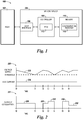
- FIG. 1 illustrates a block diagram of a computing system 100 in accordance with a number of embodiments of the present disclosure.
- computing system 100 can include a host 102 and an apparatus in the form of a memory device 104.
- an "apparatus" can refer to, but is not limited to, any of a variety of structures or combinations of structures, such as a circuit or circuitry, a die or dice, a module or modules, a device or devices, or a system or systems, for example.
- Host 102 can include a memory (e.g., a random-access memory (RAM)) and a memory access device (e.g., a processor) (not shown in Figure 1 so as not to obscure embodiments of the present disclosure).
- a processor can intend a number of processors, such as a parallel processing system, a number of coprocessors, etc.
- Example hosts can include laptop computers, personal computers, digital cameras, digital recording and playback devices, mobile devices (e.g., smart phones, tablets, etc.), PDAs, memory card readers, interface hubs, and the like.
- memory device 104 can include a host interface 106, a memory 110, and a controller 108 coupled to host interface 106 and memory 110.
- memory device 104 can be a solid state memory device. Although one memory is shown in Figure 1 , embodiments of the present disclosure are not so limited (e.g., memory device 104 can include more than one memory coupled to controller 108).
- Host interface 106 can be used to receive power from host 102, and/or to communicate information (e.g., data) between host 102 and memory device 104.
- host interface 106 can provide an interface for passing control, address, information (e.g., data), and other signals between memory device 104 and host 102, which can have compatible receptors for host interface 106.
- host interface 106 can be a physical host interface, such as a standardized physical interface.
- host interface 106 can be a serial advanced technology attachment (SATA) physical interface, a peripheral component interconnect express (PCIe) physical interface, or a universal serial bus (USB) physical interface, among other physical connectors and/or interfaces.
- SATA serial advanced technology attachment
- PCIe peripheral component interconnect express
- USB universal serial bus
- memory device 104 can receive power from, and/or communicate information with, host 102 through a wired connection with host 102 (e.g., host 102 and memory device 104 can be coupled through a wired connection).
- host interface 106 can be a wireless host interface.
- host interface 106 can include a transceiver and/or antenna that can transmit and/or receive wireless (e.g., over-the-air) signals, such as, for instance, radio frequency (RF) signals.
- RF radio frequency
- memory device 104 can receive power from, and/or communicate information with, host 102 through a wireless connection with host 102 (e.g., host 102 and memory device 104 can be wirelessly coupled).
- memory device 104 can be a wireless memory tag.
- Controller 108 can communicate with memory 110 to sense (e.g., read), program (e.g., write), and/or erase information, among other operations.
- Controller 108 can include, for example, control circuitry and/or logic (e.g., hardware and/or firmware).
- controller 108 can include a power management unit (PMU) 112, as illustrated in Figure 1 .
- PMU 112 can receive power from host 102 (e.g., through host interface 106), determine power availability information for memory 110, and provide the power and power availability information to memory 110, as will be further described herein.
- host interface 106 is a wireless host interface
- controller 108 can be an RF control unit.
- Controller 108 can be included on the same physical device (e.g., the same die) as memory 110, or can be included on a separate physical device that is communicatively coupled to the physical device that includes memory 110. In a number of embodiments, components of controller 108 can be spread across multiple physical devices (e.g., some components on the same die as memory 110, and some components on a different die, module, or board).
- Memory 110 can include, for example, a number of non-volatile memory arrays (e.g., can include a number of non-volatile memory cells).
- memory 110 can be flash memory with a NAND architecture.
- embodiments of the present disclosure are not limited to a particular type of memory.
- memory 110 can be eMultiMediaCard (eMMC) memory, universal flash storage (UFS) memory, and/or wireless memory.
- eMMC eMultiMediaCard
- UFS universal flash storage
- control gates of memory cells of a "row” can be coupled with an access (e.g., word) line, while the memory cells can be coupled in series source to drain in a "string” between a select gate source transistor and a select gate drain transistor.
- the string can be connected to a data (e.g., bit) line by the select gate drain transistor.
- the use of the terms "row” and "string” implies neither a linear nor an orthogonal arrangement of memory cells.
- the manner of connection of the memory cells to the bit lines and source lines depends on whether the array is a NAND architecture, a NOR architecture, or some other memory array architecture.
- the memory array(s) of memory 110 can include a number of memory cells that can be grouped.
- a group can include a number of memory cells, such as a page, block, plane, die, an entire array, or other groups of memory cells.
- some memory arrays can include a number of pages of memory cells that make up a block of memory cells.
- a number of blocks can be included in a plane of memory cells.
- a number of planes of memory cells can be included on a die.
- a 128 GB memory device can include 4320 bytes of information per page, 128 pages per block, 2048 blocks per plane, and 16 planes per device.
- memory device 104 can include address circuitry to latch address signals provided over I/O connectors through I/O circuitry. Address signals can be received and decoded by a row decoder and a column decoder, to access memory 110 (e.g., the array(s) of memory 110).
- controller 108 can receive power from host 102 through host interface 106. Controller 108 can receive the power from host 102 through a wired or wireless connection with host 102, as previously described herein. In embodiments in controller 108 receives power from host 102 through a wireless connection, the amount of power controller 108 receives from host 102 may depend on (e.g., vary with) the distance between host 102 and memory device 104. For example, the greater the distance between host 102 and memory device 104, the less power controller 108 may receive from host 102. Further, controller 108 may receive no power from host 102 if memory device 104 is more than a particular distance away from host 102 (e.g., if memory device 104 is outside the wireless range of host 102).
- Controller 108 can determine power availability information for memory 110. Controller 108 can determine the power availability information based on, for example, the amount of power received from host 102 and the present operating condition of memory 110. The amount of power received from host 102 can correspond to, for example, the maximum current level (e.g., amount of current at a given voltage supply level) controller 108 can provide to memory 110.
- the present operating condition of memory 110 can include, for example, the present current consumption at the given (e.g., regulated) voltage supply level (e.g., 1.8 Volts) of memory 110 (e.g., the amount of current being consumed by memory 110 during the program, sense, and/or erase operation presently being performed on memory 110).
- the power availability information for memory 110 can include, for example, an indication of whether memory 110 can continue to operate at its present operating condition. That is, the power availability information can include an indication of whether controller 108 can continue to provide enough power (e.g., current) to memory 110 for memory 110 to continue operating at its present operating condition (e.g., for the memory to continue its present program, sense, and/or erase operation).
- the power availability information can include an indication of whether controller 108 can continue to provide enough power (e.g., current) to memory 110 for memory 110 to continue operating at its present operating condition (e.g., for the memory to continue its present program, sense, and/or erase operation).
- the power availability information can include an indication memory 110 can continue to operate at its present operating condition upon controller 108 determining it is receiving enough power from host 102 to continue to provide enough power to memory 110 for it to continue operating at its present operating condition, and the power availability information can include an indication memory 110 can not continue to operate at its present operating condition upon controller 108 determining it is not receiving enough power from host 102 to continue to provide enough power to memory 110 for it to continue operating at its present operating condition.
- the power availability information may include an indication to memory 110 to freeze (e.g., pause) its operation upon the voltage supply being provided to memory 110 by controller 108 reaching (e.g., falling to) a particular (e.g., threshold) level. While the operation of memory 110 is frozen (e.g., while memory 110 is on standby), controller 108 can recover the voltage supply. Once the voltage supply is recovered (e.g., upon controller 108 determining it can provide enough power to memory 110), memory 110 can resume its operation.
- a particular (e.g., threshold) level e.g., threshold
- the power availability information may include an indication to memory 110 to abort its operation upon controller 108 ceasing to receive power from host 102.
- Controller 108 may cease to receive power from host 102, for example, upon memory device 104 being turned off (either intentionally or unintentionally), and/or upon memory device 104 being moved outside the wireless range of host 102.
- the power availability information for memory 110 may also include an indication of the amount (e.g., period) of time for which memory 110 can continue to operate at its present operating condition. That is, the power availability information can include an indication of how long controller 108 can continue to provide enough power to memory 110 for memory 110 to continue operating at its present operating condition.
- the amount of time for which memory 110 can continue to operate at its present operating condition can be the amount of time for which memory 110 can continue its present current consumption before the voltage supply controller 108 provides to memory 110 reaches (e.g., falls to) a particular (e.g., threshold) level.
- the amount of time can be one of a number of amounts of time. For instance, the amount of time can be unlimited, long, intermediate or short.
- the power availability information may include an indication memory 110 can continue to operate at its present operating condition for an unlimited amount of time, a first (e.g., long) amount of time that is less than the unlimited amount of time, a second (e.g., intermediate) amount of time that is less than the first amount of time, or a third (e.g., short) amount of time that is less than the second amount of time.
- the different amounts of time may depend on, for example, the characteristics (e.g., technology, architecture, performance, etc.) of memory 110.
- the first, second, and third amounts of time can be 75 microseconds, 50 microseconds, and 25 microseconds, respectively.
- embodiments of the present disclosure are not limited to particular amounts of time, or to a particular number of amounts of time.
- controller 108 can provide power (e.g., the power received from host 102) and the determined power availability information to memory 110. That is, memory 110 can receive power and the determined power availability information from controller 108.
- controller 108 can represent the power availability information using a number of binary data values (e.g., bits), and communicate (e.g., send) the data values to memory 110.
- the power availability information includes an indication of whether memory 110 can continue to operate at its present operating condition
- an indication memory 110 can continue to operate at its present operating condition can be represented by data value 0
- an indication memory 110 can not continue to operate at its present operating condition can be represented by data value 1.
- an indication memory 110 can continue to operate at its present operating condition for an unlimited amount of time can be represented by data value 000, an indication memory 110 can continue to operate at its present operating condition for a long amount of time can be represented by data value 001, an indication memory 110 can continue to operate at its present operating condition for an intermediate amount of time can be represented by data value 010, and an indication memory 110 can continue to operate at its present operating condition for a short amount of time can be represented by data value 011.
- an indication to memory 110 to freeze its operation can be represented by data value 100, 101, or 110, and in indication to memory 110 to abort its operation can be represented by data value 111.
- embodiments of the present disclosure are not limited to particular data values or combinations of data values.
- memory 110 includes a configuration register 114.
- controller 108 can provide the power availability information to memory 110 through configuration register 114.
- controller 108 can provide the power availability information to memory 110 through a number of interface signals (e.g., address signals, data signals, etc.).
- memory 110 can determine whether to adjust its operation based, at least in part, on the power availability information received from controller 108. For example, memory 110 can continue to operate at its present operating condition (e.g., continue its present program, sense, and/or erase operation) upon the power availability information including an indication memory 110 can continue to operate at its present operating condition, and memory 110 can cease operating at its present operating condition (e.g., abort or freeze its present program, sense, and/or erase operation) upon the power availability information including an indication memory 110 can not continue to operate at its present operating condition. As an additional example, upon the power availability information including an indication memory 110 can continue to operate at its present operating condition for an amount of time, memory 110 can continue to operate at its present operating condition for the amount of time.
- present operating condition e.g., continue its present program, sense, and/or erase operation
- memory 110 can cease operating at its present operating condition (e.g., abort or freeze its present program, sense, and/or erase operation) upon the power availability information including an indication memory 110 can not continue
- Controller 108 can continue to determine and provide power availability information to memory 110 during operation of memory device 104. For example, controller 108 can determine and provide additional (e.g., updated) power availability information to memory 110 upon (e.g., based on) a change in the amount of power received from host 102, and/or upon a change in the operating condition of memory 110. That is, controller 108 can determine and provide additional power availability information to memory 110 upon a change in the maximum current level at a given voltage supply controller 108 can provide to memory 110, and/or upon a change in current consumption by (e.g., the current consumption level of) memory 110.
- additional (e.g., updated) power availability information to memory 110 upon (e.g., based on) a change in the amount of power received from host 102, and/or upon a change in the operating condition of memory 110. That is, controller 108 can determine and provide additional power availability information to memory 110 upon a change in the maximum current level at a given voltage supply controller 108 can provide to memory 110, and
- controller 108 can determine and provide additional power availability information to memory 110 upon the voltage supply that controller 108 provides to memory 110 reaching (e.g., falling to) a particular (e.g., threshold) level.
- the additional power availability information can include, for example, an indication of whether, and/or the amount of time for which, memory 110 can continue to operate at its present operating condition, in a manner analogous to the power availability information previously described herein.
- memory 110 can determine whether to adjust its operation based, at least in part, on the additional power availability information, in a manner analogous to that previously described herein.
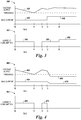
- Figure 2 illustrates an example of timing diagrams 220 and 221 associated with providing power availability information to memory in accordance with a number of embodiments of the present disclosure.
- the memory can be, for example, memory 110 previously described in connection with Figure 1 .
- timing diagram 220 includes waveform 222, which represents the amount of voltage supply a controller in communication with the memory (e.g., controller 108 previously described in connection with Figure 1 ) is providing (e.g., supplying) to the memory during operation of the memory.
- Timing diagram 220 also includes waveform 224, which represents the maximum current level at a given voltage supply (e.g., 1.8 Volts) the controller can provide to the memory during the operation of the memory.
- the maximum current level at the given voltage supply can correspond to the amount of power the controller receives from a host, as previously described herein (e.g., in connection with Figure 1 ).
- timing diagram 221 includes waveform 226, which represents the current consumption by the memory during the operation of the memory.
- the current consumption at the given voltage supply by the memory is at a higher level than the maximum current level at the given voltage supply the controller can provide to the memory.
- the current consumption by the memory at time t0 may be 50 milliamps (mA), but the maximum current level at the given voltage supply the controller can provide to the memory at time t0 may only be 25 mA.
- the controller may provide power availability information to the memory that indicates the memory can only continue to operate at its present operating condition (e.g., its present current consumption level) for a particular amount of time before the voltage supply the controller provides to the memory reaches (e.g., falls to) the threshold level illustrated in Figure 2 .
- the particular amount of time can be, for example, one of a number of amounts of time, such as, for instance, a long amount of time, as previously described herein (e.g., in connection with Figure 1 ).
- the memory may continue to operate at its present operating condition (e.g., may continue to consume 50 mA of current) for the particular amount of time (e.g., from time t0 to time t1), as illustrated in Figure 2 .
- the controller may provide power availability information to the memory that includes an indication to the memory to freeze (e.g., pause) its operation.
- the memory may freeze its operation (e.g., move to standby and/or consume no current) at time t1, as illustrated in Figure 2 . While the operation of the memory is frozen (e.g., from time t1 to time t2), the controller can recover its voltage supply, as illustrated in Figure 2 .
- the controller may again provide power availability information to the memory that indicates the memory can only continue to operate at its present operating condition for the particular amount of (e.g., long) time before the voltage supply the controller provides to the memory reaches the threshold level.
- the memory may continue to operate at its present operating condition, as illustrated in Figure 2 .
- the memory has increased its current consumption to level 230 (e.g., 70 mA), as illustrated in Figure 2 .
- This increase may be a result of, for example, a change in the operation of (e.g., being performed on) the memory.
- the controller may provide power availability information to the memory that indicates the memory can only continue to operate at that operating condition (e.g., current consumption level 230) for a shorter amount of time before the voltage supply the controller provides to the memory reaches the threshold level.
- the shorter amount of time can be a different one of the amounts of time, such as, for instance, a short amount of time, as previously described herein.
- the memory may continue to operate at its present operating condition (e.g., may continue to consume 70 mA of current) for the shorter amount of time (e.g., from time t3 to time t4), as illustrated in Figure 2 .
- the controller may provide power availability information to the memory that includes an indication to the memory to freeze its operation.
- the memory may freeze its operation at time t4, as illustrated in Figure 2 . While the operation of the memory is frozen (e.g., from time t4 to time t5), the controller can recover its voltage supply, as illustrated in Figure 2 .
- the controller may again provide power availability information to the memory that indicates the memory can only continue to operate at its present operating condition for the shorter time before the voltage supply the controller provides to the memory reaches the threshold level.
- the memory may continue to operate at its present operating condition, as illustrated in Figure 2 .
- the memory has decreased its current consumption at the given voltage supply to level 232 (e.g., 20 mA), as illustrated in Figure 2 , which is below (e.g., less than) the maximum current level (e.g., 25 mA) at the given voltage supply the controller can provide to the memory.
- This decrease may be a result of, for example, a change in the operation of (e.g., being performed on) the memory
- the controller may provide power availability information to the memory that indicates the memory can continue to operate at its present operating condition for an unlimited amount of time.
- the memory may continue to operate at its present operating condition (e.g., may continue to consume 20 mA of current), as illustrated in Figure 2 .
- Figure 3 illustrates an example of timing diagrams 340 and 341 associated with providing power availability information to memory in accordance with a number of embodiments of the present disclosure.
- the memory can be, for example, memory 110 previously described in connection with Figure 1 .
- timing diagram 340 includes waveform 342, which represents the amount of voltage supply a controller in communication with the memory (e.g., controller 108 previously described in connection with Figure 1 ) is providing (e.g., supplying) to the memory during operation of the memory.
- Timing diagram 340 also includes waveform 344, which represents the maximum current level at a given voltage supply (e.g., 1.8 Volts) the controller can provide to the memory during the operation of the memory.
- the maximum current level at the given voltage supply can correspond to the amount of power the controller receives from a host, as previously described herein (e.g., in connection with Figure 1 ).
- timing diagram 341 includes waveform 346, which represents the current consumption by the memory during the operation of the memory. From initial time t0 to time t3 in the example illustrated in Figure 3 , timing diagrams 340 and 341 can be analogous to timing diagrams 220 and 221, respectively, previously described in connection with Figure 2 from initial time t0 to time t3.
- the maximum current level at the given voltage supply the controller can provide to the memory has increased to level 348 (e.g., 100 mA), as illustrated in Figure 3 , which is above (e.g., greater than) the current consumption by the memory at time t3 (e.g., current consumption level 350).
- level 348 e.g., 100 mA
- the controller may provide power availability information to the memory that indicates the memory can continue to operate at its present operating condition for an unlimited amount of time.
- the memory may continue to operate at its present operating condition (e.g., current consumption level 350), as illustrated in Figure 3 .
- the memory has increased its current consumption at the given voltage supply to level 352 (e.g., 70 mA), as illustrated in Figure 3 .
- This increase may be a result of, for example, a change in the operation of (e.g., being performed on) the memory.
- the controller can provide to the memory at time t4 (e.g., 100 mA), no additional (e.g., updated) power availability information may be provided to the memory by the controller, and the memory may continue to operate at its present operating condition (e.g., current consumption level 352), as illustrated in Figure 3 .
- Figure 4 illustrates an example of timing diagrams 460 and 461 associated with providing power availability information to memory in accordance with a number of embodiments of the present disclosure.
- the memory can be, for example, memory 110 previously described in connection with Figure 1 .
- timing diagram 460 includes waveform 462, which represents the amount voltage supply a controller in communication with the memory (e.g., controller 108 previously described in connection with Figure 1 ) is providing (e.g., supplying) to the memory during operation of the memory.
- Timing diagram 460 also includes waveform 464, which represents the maximum current level at a given voltage supply the controller can provide to the memory during the operation of the memory. The maximum current level at the given voltage supply can correspond to the amount of power the controller receives from a host, as previously described herein (e.g., in connection with Figure 1 ).
- timing diagram 461 includes waveform 466, which represents the current consumption by the memory during the operation of the memory. From initial time t0 to time t3 in the example illustrated in Figure 4 , timing diagrams 460 and 461 can be analogous to timing diagrams 220 and 221, respectively, previously described in connection with Figure 2 from initial time tO to time t3.
- the controller has ceased to receive power from the host.
- the amount of power being provided to the memory by the controller and the maximum current level at the voltage supply the controller can provide to the memory decrease to levels 468 and 470 (e.g., zero), respectively, as shown in Figure 4 .
- the controller may provide power availability information to the memory that includes an indication to the memory to abort its operation.
- the memory may abort its operation (e.g., reduce its current consumption from level 472 to zero) at time t3, as illustrated in Figure 4 .
Landscapes
- Engineering & Computer Science (AREA)
- Power Engineering (AREA)
- Theoretical Computer Science (AREA)
- Physics & Mathematics (AREA)
- General Engineering & Computer Science (AREA)
- General Physics & Mathematics (AREA)
- Microelectronics & Electronic Packaging (AREA)
- Computer Hardware Design (AREA)
- Power Sources (AREA)
- Memory System (AREA)
Abstract
Description
- The present disclosure relates generally to semiconductor memory and methods, and more particularly, to providing power availability information to memory.
- Memory devices are typically provided as internal, semiconductor, integrated circuits and/or external removable devices in computers or other electronic devices. There are many different types of memory including volatile and non-volatile memory. Volatile memory can require power to maintain its data and can include random-access memory (RAM), dynamic random access memory (DRAM), and synchronous dynamic random access memory (SDRAM), among others. Non-volatile memory can retain stored data when not powered and can include NAND flash memory, NOR flash memory, phase change random access memory (PCRAM), resistive random access memory (RRAM), and magnetic random access memory (MRAM), among others.
- Memory devices can be combined together to form a solid state drive (SSD). An SSD can include non-volatile memory (e.g., NAND flash memory, NOR flash memory, eMultiMediaCard (eMMC) memory, universal flash storage (UFS) memory, and/or wireless memory), and/or can include volatile memory (e.g., DRAM and/or SRAM), among various other types of non-volatile and volatile memory. Flash memory devices can include memory cells storing data in a charge storage structure such as a floating gate, for instance, and may be utilized as non-volatile memory for a wide range of electronic applications. Flash memory devices may use a one-transistor memory cell that allows for high memory densities, high reliability, and low power consumption.
- Memory cells in an array architecture can be programmed to a target (e.g., desired) state. For instance, electric charge can be placed on or removed from the charge storage structure (e.g., floating gate) of a memory cell to program the cell to a particular data state. The stored charge on the charge storage structure of the memory cell can indicate a threshold voltage (Vt) of the cell, and the state (e.g., data state) of the memory cell can be determined by sensing the stored charge on the charge storage structure (e.g., the Vt) of the cell.
- Memory may consume power (e.g., current at a regulated voltage supply) while operating, such as during program, sense, and/or erase operations performed on the cells of the memory. This power can be provided to the memory by, for example, a host. However, the memory may not be aware of how much (e.g., the maximum amount of) power the host can provide to the memory, and accordingly the memory may not be aware of whether it will have enough power to sustain its present operation. If the memory's power consumption during operation exceeds the amount of power that can be provided by the host, the memory's operation may fail.
-
-
Figure 1 illustrates a block diagram of a computing system in accordance with a number of embodiments of the present disclosure. -
Figure 2 illustrates an example of timing diagrams associated with providing power availability information to memory in accordance with a number of embodiments of the present disclosure. -
Figure 3 illustrates an example of timing diagrams associated with providing power availability information to memory in accordance with a number of embodiments of the present disclosure. -
Figure 4 illustrates an example of timing diagrams associated with providing power availability information to memory in accordance with a number of embodiments of the present disclosure. - The present disclosure includes apparatuses and methods for providing power availability information to memory. A number of embodiments include a memory and a controller. The controller is configured to provide power and power availability information to the memory, and the memory is configured to determine whether to adjust its operation based, at least in part, on the power availability information.
- Providing power availability information to memory in accordance with the present disclosure can inform the memory of whether, and/or the amount of time for which, the memory can continue to operate (e.g., have enough power to continue operating) at its present operating condition (e.g., present power consumption). If the power availability information indicates the memory may not be able to continue to operate at its present operation condition, the memory can adjust its operation accordingly, and thereby avoid failure.
- As used herein, "a number of' something can refer to one or more such things. For example, a number of memory cells can refer to one or more memory cells.
- The figures herein follow a numbering convention in which the first digit or digits correspond to the drawing figure number and the remaining digits identify an element or component in the drawing. Similar elements or components between different figures may be identified by the use of similar digits.
-
Figure 1 illustrates a block diagram of acomputing system 100 in accordance with a number of embodiments of the present disclosure. As shown inFigure 1 ,computing system 100 can include ahost 102 and an apparatus in the form of amemory device 104. As used herein, an "apparatus" can refer to, but is not limited to, any of a variety of structures or combinations of structures, such as a circuit or circuitry, a die or dice, a module or modules, a device or devices, or a system or systems, for example. -
Host 102 can include a memory (e.g., a random-access memory (RAM)) and a memory access device (e.g., a processor) (not shown inFigure 1 so as not to obscure embodiments of the present disclosure). One of ordinary skill in the art will appreciate that "a processor" can intend a number of processors, such as a parallel processing system, a number of coprocessors, etc. Example hosts can include laptop computers, personal computers, digital cameras, digital recording and playback devices, mobile devices (e.g., smart phones, tablets, etc.), PDAs, memory card readers, interface hubs, and the like. - As shown in
Figure 1 ,memory device 104 can include ahost interface 106, amemory 110, and acontroller 108 coupled tohost interface 106 andmemory 110. In a number of embodiments,memory device 104 can be a solid state memory device. Although one memory is shown inFigure 1 , embodiments of the present disclosure are not so limited (e.g.,memory device 104 can include more than one memory coupled to controller 108). -
Host interface 106 can be used to receive power fromhost 102, and/or to communicate information (e.g., data) betweenhost 102 andmemory device 104. For example,host interface 106 can provide an interface for passing control, address, information (e.g., data), and other signals betweenmemory device 104 andhost 102, which can have compatible receptors forhost interface 106. - In a number of embodiments,
host interface 106 can be a physical host interface, such as a standardized physical interface. For example, whenmemory device 104 is used for information storage incomputing system 100,host interface 106 can be a serial advanced technology attachment (SATA) physical interface, a peripheral component interconnect express (PCIe) physical interface, or a universal serial bus (USB) physical interface, among other physical connectors and/or interfaces. In such embodiments,memory device 104 can receive power from, and/or communicate information with,host 102 through a wired connection with host 102 (e.g.,host 102 andmemory device 104 can be coupled through a wired connection). - In a number of embodiments,
host interface 106 can be a wireless host interface. For example,host interface 106 can include a transceiver and/or antenna that can transmit and/or receive wireless (e.g., over-the-air) signals, such as, for instance, radio frequency (RF) signals. In such embodiments,memory device 104 can receive power from, and/or communicate information with,host 102 through a wireless connection with host 102 (e.g.,host 102 andmemory device 104 can be wirelessly coupled). For example, in such embodiments,memory device 104 can be a wireless memory tag. -
Controller 108 can communicate withmemory 110 to sense (e.g., read), program (e.g., write), and/or erase information, among other operations.Controller 108 can include, for example, control circuitry and/or logic (e.g., hardware and/or firmware). For instance,controller 108 can include a power management unit (PMU) 112, as illustrated inFigure 1 . PMU 112 can receive power from host 102 (e.g., through host interface 106), determine power availability information formemory 110, and provide the power and power availability information tomemory 110, as will be further described herein. In embodiments in whichhost interface 106 is a wireless host interface (e.g., in embodiments in whichmemory device 104 is a wireless memory tag),controller 108 can be an RF control unit. -
Controller 108 can be included on the same physical device (e.g., the same die) asmemory 110, or can be included on a separate physical device that is communicatively coupled to the physical device that includesmemory 110. In a number of embodiments, components ofcontroller 108 can be spread across multiple physical devices (e.g., some components on the same die asmemory 110, and some components on a different die, module, or board). -
Memory 110 can include, for example, a number of non-volatile memory arrays (e.g., can include a number of non-volatile memory cells). For instance,memory 110 can be flash memory with a NAND architecture. However, embodiments of the present disclosure are not limited to a particular type of memory. For example, in a number of embodiments,memory 110 can be eMultiMediaCard (eMMC) memory, universal flash storage (UFS) memory, and/or wireless memory. - In a NAND architecture, the control gates of memory cells of a "row" can be coupled with an access (e.g., word) line, while the memory cells can be coupled in series source to drain in a "string" between a select gate source transistor and a select gate drain transistor. The string can be connected to a data (e.g., bit) line by the select gate drain transistor. The use of the terms "row" and "string" implies neither a linear nor an orthogonal arrangement of memory cells. As will be appreciated by those of ordinary skill in the art, the manner of connection of the memory cells to the bit lines and source lines depends on whether the array is a NAND architecture, a NOR architecture, or some other memory array architecture.
- The memory array(s) of
memory 110 can include a number of memory cells that can be grouped. As used herein, a group can include a number of memory cells, such as a page, block, plane, die, an entire array, or other groups of memory cells. For example, some memory arrays can include a number of pages of memory cells that make up a block of memory cells. A number of blocks can be included in a plane of memory cells. A number of planes of memory cells can be included on a die. As an example, a 128 GB memory device can include 4320 bytes of information per page, 128 pages per block, 2048 blocks per plane, and 16 planes per device. - The embodiment illustrated in
Figure 1 can include additional circuitry that is not illustrated so as not to obscure embodiments of the present disclosure. For example,memory device 104 can include address circuitry to latch address signals provided over I/O connectors through I/O circuitry. Address signals can be received and decoded by a row decoder and a column decoder, to access memory 110 (e.g., the array(s) of memory 110). - In a number of embodiments, controller 108 (e.g., PMU 112) can receive power from
host 102 throughhost interface 106.Controller 108 can receive the power fromhost 102 through a wired or wireless connection withhost 102, as previously described herein. In embodiments incontroller 108 receives power fromhost 102 through a wireless connection, the amount ofpower controller 108 receives fromhost 102 may depend on (e.g., vary with) the distance betweenhost 102 andmemory device 104. For example, the greater the distance betweenhost 102 andmemory device 104, theless power controller 108 may receive fromhost 102. Further,controller 108 may receive no power fromhost 102 ifmemory device 104 is more than a particular distance away from host 102 (e.g., ifmemory device 104 is outside the wireless range of host 102). - Controller 108 (e.g., PMU 112) can determine power availability information for
memory 110.Controller 108 can determine the power availability information based on, for example, the amount of power received fromhost 102 and the present operating condition ofmemory 110. The amount of power received fromhost 102 can correspond to, for example, the maximum current level (e.g., amount of current at a given voltage supply level)controller 108 can provide tomemory 110. The present operating condition ofmemory 110 can include, for example, the present current consumption at the given (e.g., regulated) voltage supply level (e.g., 1.8 Volts) of memory 110 (e.g., the amount of current being consumed bymemory 110 during the program, sense, and/or erase operation presently being performed on memory 110). - The power availability information for
memory 110 can include, for example, an indication of whethermemory 110 can continue to operate at its present operating condition. That is, the power availability information can include an indication of whethercontroller 108 can continue to provide enough power (e.g., current) tomemory 110 formemory 110 to continue operating at its present operating condition (e.g., for the memory to continue its present program, sense, and/or erase operation). For example, the power availability information can include anindication memory 110 can continue to operate at its present operating condition uponcontroller 108 determining it is receiving enough power fromhost 102 to continue to provide enough power tomemory 110 for it to continue operating at its present operating condition, and the power availability information can include anindication memory 110 can not continue to operate at its present operating condition uponcontroller 108 determining it is not receiving enough power fromhost 102 to continue to provide enough power tomemory 110 for it to continue operating at its present operating condition. - As an example, the power availability information may include an indication to
memory 110 to freeze (e.g., pause) its operation upon the voltage supply being provided tomemory 110 bycontroller 108 reaching (e.g., falling to) a particular (e.g., threshold) level. While the operation ofmemory 110 is frozen (e.g., whilememory 110 is on standby),controller 108 can recover the voltage supply. Once the voltage supply is recovered (e.g., uponcontroller 108 determining it can provide enough power to memory 110),memory 110 can resume its operation. - As an additional example, the power availability information may include an indication to
memory 110 to abort its operation uponcontroller 108 ceasing to receive power fromhost 102.Controller 108 may cease to receive power fromhost 102, for example, uponmemory device 104 being turned off (either intentionally or unintentionally), and/or uponmemory device 104 being moved outside the wireless range ofhost 102. - The power availability information for
memory 110 may also include an indication of the amount (e.g., period) of time for whichmemory 110 can continue to operate at its present operating condition. That is, the power availability information can include an indication of howlong controller 108 can continue to provide enough power tomemory 110 formemory 110 to continue operating at its present operating condition. - For example, the amount of time for which
memory 110 can continue to operate at its present operating condition can be the amount of time for whichmemory 110 can continue its present current consumption before thevoltage supply controller 108 provides tomemory 110 reaches (e.g., falls to) a particular (e.g., threshold) level. Further, the amount of time can be one of a number of amounts of time. For instance, the amount of time can be unlimited, long, intermediate or short. That is, in such an example, the power availability information may include anindication memory 110 can continue to operate at its present operating condition for an unlimited amount of time, a first (e.g., long) amount of time that is less than the unlimited amount of time, a second (e.g., intermediate) amount of time that is less than the first amount of time, or a third (e.g., short) amount of time that is less than the second amount of time. The different amounts of time may depend on, for example, the characteristics (e.g., technology, architecture, performance, etc.) ofmemory 110. As an example, the first, second, and third amounts of time can be 75 microseconds, 50 microseconds, and 25 microseconds, respectively. However, embodiments of the present disclosure are not limited to particular amounts of time, or to a particular number of amounts of time. - In a number of embodiments, controller 108 (e.g., PMU 112) can provide power (e.g., the power received from host 102) and the determined power availability information to
memory 110. That is,memory 110 can receive power and the determined power availability information fromcontroller 108. For instance,controller 108 can represent the power availability information using a number of binary data values (e.g., bits), and communicate (e.g., send) the data values tomemory 110. As an example, in embodiments in which the power availability information includes an indication of whethermemory 110 can continue to operate at its present operating condition, anindication memory 110 can continue to operate at its present operating condition can be represented by data value 0, and anindication memory 110 can not continue to operate at its present operating condition can be represented by data value 1. - As an additional example, in embodiments in which the power availability information includes an indication of the amount of time for which
memory 110 can continue to operate at its present operating condition, anindication memory 110 can continue to operate at its present operating condition for an unlimited amount of time can be represented by data value 000, anindication memory 110 can continue to operate at its present operating condition for a long amount of time can be represented by data value 001, anindication memory 110 can continue to operate at its present operating condition for an intermediate amount of time can be represented by data value 010, and anindication memory 110 can continue to operate at its present operating condition for a short amount of time can be represented by data value 011. Further, in such embodiments, an indication tomemory 110 to freeze its operation can be represented bydata value memory 110 to abort its operation can be represented by data value 111. However, embodiments of the present disclosure are not limited to particular data values or combinations of data values. - In the embodiment illustrated in
Figure 1 ,memory 110 includes aconfiguration register 114. In such an embodiment,controller 108 can provide the power availability information tomemory 110 throughconfiguration register 114. As an additional example,controller 108 can provide the power availability information tomemory 110 through a number of interface signals (e.g., address signals, data signals, etc.). - In a number of embodiments,
memory 110 can determine whether to adjust its operation based, at least in part, on the power availability information received fromcontroller 108. For example,memory 110 can continue to operate at its present operating condition (e.g., continue its present program, sense, and/or erase operation) upon the power availability information including anindication memory 110 can continue to operate at its present operating condition, andmemory 110 can cease operating at its present operating condition (e.g., abort or freeze its present program, sense, and/or erase operation) upon the power availability information including anindication memory 110 can not continue to operate at its present operating condition. As an additional example, upon the power availability information including anindication memory 110 can continue to operate at its present operating condition for an amount of time,memory 110 can continue to operate at its present operating condition for the amount of time. -
Controller 108 can continue to determine and provide power availability information tomemory 110 during operation ofmemory device 104. For example,controller 108 can determine and provide additional (e.g., updated) power availability information tomemory 110 upon (e.g., based on) a change in the amount of power received fromhost 102, and/or upon a change in the operating condition ofmemory 110. That is,controller 108 can determine and provide additional power availability information tomemory 110 upon a change in the maximum current level at a givenvoltage supply controller 108 can provide tomemory 110, and/or upon a change in current consumption by (e.g., the current consumption level of)memory 110. Further,controller 108 can determine and provide additional power availability information tomemory 110 upon the voltage supply thatcontroller 108 provides tomemory 110 reaching (e.g., falling to) a particular (e.g., threshold) level. The additional power availability information can include, for example, an indication of whether, and/or the amount of time for which,memory 110 can continue to operate at its present operating condition, in a manner analogous to the power availability information previously described herein. Upon receiving the additional power availability information,memory 110 can determine whether to adjust its operation based, at least in part, on the additional power availability information, in a manner analogous to that previously described herein. -
Figure 2 illustrates an example of timing diagrams 220 and 221 associated with providing power availability information to memory in accordance with a number of embodiments of the present disclosure. The memory can be, for example,memory 110 previously described in connection withFigure 1 . - As shown in
Figure 2 , timing diagram 220 includeswaveform 222, which represents the amount of voltage supply a controller in communication with the memory (e.g.,controller 108 previously described in connection withFigure 1 ) is providing (e.g., supplying) to the memory during operation of the memory. Timing diagram 220 also includeswaveform 224, which represents the maximum current level at a given voltage supply (e.g., 1.8 Volts) the controller can provide to the memory during the operation of the memory. The maximum current level at the given voltage supply can correspond to the amount of power the controller receives from a host, as previously described herein (e.g., in connection withFigure 1 ). In the example illustrated inFigure 2 , the maximum current level at the given voltage supply remains constant (e.g., the same) throughout the operation of the memory. As shown inFigure 2 , timing diagram 221 includeswaveform 226, which represents the current consumption by the memory during the operation of the memory. - At initial time t0 in the example illustrated in
Figure 2 , the current consumption at the given voltage supply by the memory is at a higher level than the maximum current level at the given voltage supply the controller can provide to the memory. For instance, the current consumption by the memory at time t0 may be 50 milliamps (mA), but the maximum current level at the given voltage supply the controller can provide to the memory at time t0 may only be 25 mA. As such, the controller may provide power availability information to the memory that indicates the memory can only continue to operate at its present operating condition (e.g., its present current consumption level) for a particular amount of time before the voltage supply the controller provides to the memory reaches (e.g., falls to) the threshold level illustrated inFigure 2 . The particular amount of time can be, for example, one of a number of amounts of time, such as, for instance, a long amount of time, as previously described herein (e.g., in connection withFigure 1 ). In response to receiving the power availability information from the controller, the memory may continue to operate at its present operating condition (e.g., may continue to consume 50 mA of current) for the particular amount of time (e.g., from time t0 to time t1), as illustrated inFigure 2 . - At time t1, the voltage supply being provided to the memory by the controller reaches the threshold level, as illustrated in
Figure 2 . As such, the controller may provide power availability information to the memory that includes an indication to the memory to freeze (e.g., pause) its operation. In response to receiving this power availability information, the memory may freeze its operation (e.g., move to standby and/or consume no current) at time t1, as illustrated inFigure 2 . While the operation of the memory is frozen (e.g., from time t1 to time t2), the controller can recover its voltage supply, as illustrated inFigure 2 . - At time t2, the voltage supply of the controller has been fully recovered, and the memory has resumed its operation at current consumption level 228 (e.g., 50 mA), as illustrated in
Figure 2 . As such, the controller may again provide power availability information to the memory that indicates the memory can only continue to operate at its present operating condition for the particular amount of (e.g., long) time before the voltage supply the controller provides to the memory reaches the threshold level. In response to receiving the power availability information from the controller, the memory may continue to operate at its present operating condition, as illustrated inFigure 2 . - At time t3, the memory has increased its current consumption to level 230 (e.g., 70 mA), as illustrated in
Figure 2 . This increase may be a result of, for example, a change in the operation of (e.g., being performed on) the memory. As a result of this increase, the controller may provide power availability information to the memory that indicates the memory can only continue to operate at that operating condition (e.g., current consumption level 230) for a shorter amount of time before the voltage supply the controller provides to the memory reaches the threshold level. The shorter amount of time can be a different one of the amounts of time, such as, for instance, a short amount of time, as previously described herein. In response to receiving this power availability information from the controller, the memory may continue to operate at its present operating condition (e.g., may continue to consume 70 mA of current) for the shorter amount of time (e.g., from time t3 to time t4), as illustrated inFigure 2 . - At time t4, the voltage supply being provided to the memory by the controller reaches the threshold level, as illustrated in
Figure 2 . As such, the controller may provide power availability information to the memory that includes an indication to the memory to freeze its operation. In response to receiving this power availability information, the memory may freeze its operation at time t4, as illustrated inFigure 2 . While the operation of the memory is frozen (e.g., from time t4 to time t5), the controller can recover its voltage supply, as illustrated inFigure 2 . - At time t5, the voltage supply of the controller has been fully recovered, and the memory has resumed its operation at current consumption level 230 (e.g., 70 mA) at the given voltage supply, as illustrated in
Figure 2 . As such, the controller may again provide power availability information to the memory that indicates the memory can only continue to operate at its present operating condition for the shorter time before the voltage supply the controller provides to the memory reaches the threshold level. In response to receiving this power availability information from the controller, the memory may continue to operate at its present operating condition, as illustrated inFigure 2 . - At time t6, the memory has decreased its current consumption at the given voltage supply to level 232 (e.g., 20 mA), as illustrated in
Figure 2 , which is below (e.g., less than) the maximum current level (e.g., 25 mA) at the given voltage supply the controller can provide to the memory. This decrease may be a result of, for example, a change in the operation of (e.g., being performed on) the memory As a result of this decrease, the controller may provide power availability information to the memory that indicates the memory can continue to operate at its present operating condition for an unlimited amount of time. In response to receiving this power availability information from the controller, the memory may continue to operate at its present operating condition (e.g., may continue to consume 20 mA of current), as illustrated inFigure 2 . -
Figure 3 illustrates an example of timing diagrams 340 and 341 associated with providing power availability information to memory in accordance with a number of embodiments of the present disclosure. The memory can be, for example,memory 110 previously described in connection withFigure 1 . - As shown in
Figure 3 , timing diagram 340 includeswaveform 342, which represents the amount of voltage supply a controller in communication with the memory (e.g.,controller 108 previously described in connection withFigure 1 ) is providing (e.g., supplying) to the memory during operation of the memory. Timing diagram 340 also includeswaveform 344, which represents the maximum current level at a given voltage supply (e.g., 1.8 Volts) the controller can provide to the memory during the operation of the memory. The maximum current level at the given voltage supply can correspond to the amount of power the controller receives from a host, as previously described herein (e.g., in connection withFigure 1 ). As shown inFigure 3 , timing diagram 341 includeswaveform 346, which represents the current consumption by the memory during the operation of the memory. From initial time t0 to time t3 in the example illustrated inFigure 3 , timing diagrams 340 and 341 can be analogous to timing diagrams 220 and 221, respectively, previously described in connection withFigure 2 from initial time t0 to time t3. - At time t3, the maximum current level at the given voltage supply the controller can provide to the memory has increased to level 348 (e.g., 100 mA), as illustrated in
Figure 3 , which is above (e.g., greater than) the current consumption by the memory at time t3 (e.g., current consumption level 350). This increase may be a result of, for example, the memory and/or controller being moved closer to the host in embodiments in which the controller receives power from the host through a wireless connection. As a result of this increase, the controller may provide power availability information to the memory that indicates the memory can continue to operate at its present operating condition for an unlimited amount of time. In response to receiving this power availability information from the controller, the memory may continue to operate at its present operating condition (e.g., current consumption level 350), as illustrated inFigure 3 . - At time t4, the memory has increased its current consumption at the given voltage supply to level 352 (e.g., 70 mA), as illustrated in
Figure 3 . This increase may be a result of, for example, a change in the operation of (e.g., being performed on) the memory. However, because this increase does not result in the memory's current consumption at the regulated voltage supply exceeding the maximum current level the controller can provide to the memory at time t4 (e.g., 100 mA), no additional (e.g., updated) power availability information may be provided to the memory by the controller, and the memory may continue to operate at its present operating condition (e.g., current consumption level 352), as illustrated inFigure 3 . -
Figure 4 illustrates an example of timing diagrams 460 and 461 associated with providing power availability information to memory in accordance with a number of embodiments of the present disclosure. The memory can be, for example,memory 110 previously described in connection withFigure 1 . - As shown in
Figure 4 , timing diagram 460 includeswaveform 462, which represents the amount voltage supply a controller in communication with the memory (e.g.,controller 108 previously described in connection withFigure 1 ) is providing (e.g., supplying) to the memory during operation of the memory. Timing diagram 460 also includeswaveform 464, which represents the maximum current level at a given voltage supply the controller can provide to the memory during the operation of the memory. The maximum current level at the given voltage supply can correspond to the amount of power the controller receives from a host, as previously described herein (e.g., in connection withFigure 1 ). As shown inFigure 4 , timing diagram 461 includeswaveform 466, which represents the current consumption by the memory during the operation of the memory. From initial time t0 to time t3 in the example illustrated inFigure 4 , timing diagrams 460 and 461 can be analogous to timing diagrams 220 and 221, respectively, previously described in connection withFigure 2 from initial time tO to time t3. - At time t3 in the example illustrated in
Figure 4 , the controller has ceased to receive power from the host. As such, the amount of power being provided to the memory by the controller and the maximum current level at the voltage supply the controller can provide to the memory decrease tolevels 468 and 470 (e.g., zero), respectively, as shown inFigure 4 . Further, upon the controller ceasing to receive power from the host, the controller may provide power availability information to the memory that includes an indication to the memory to abort its operation. In response to receiving this power availability information, the memory may abort its operation (e.g., reduce its current consumption fromlevel 472 to zero) at time t3, as illustrated inFigure 4 . - Although specific embodiments have been illustrated and described herein, those of ordinary skill in the art will appreciate that an arrangement calculated to achieve the same results can be substituted for the specific embodiments shown. This disclosure is intended to cover adaptations or variations of a number of embodiments of the present disclosure. It is to be understood that the above description has been made in an illustrative fashion, and not a restrictive one. Combination of the above embodiments, and other embodiments not specifically described herein will be apparent to those of ordinary skill in the art upon reviewing the above description. The scope of a number of embodiments of the present disclosure includes other applications in which the above structures and methods are used. Therefore, the scope of a number of embodiments of the present disclosure should be determined with reference to the appended claims, along with the full range of equivalents to which such claims are entitled.
- In the foregoing Detailed Description, some features are grouped together in a single embodiment for the purpose of streamlining the disclosure. This method of disclosure is not to be interpreted as reflecting an intention that the disclosed embodiments of the present disclosure have to use more features than are expressly recited in each claim. Rather, as the following claims reflect, inventive subject matter lies in less than all features of a single disclosed embodiment. Thus, the following claims are hereby incorporated into the Detailed Description, with each claim standing on its own as a separate embodiment.
- The present disclosure also includes the content of the following clauses:
- 1. An apparatus, comprising:
- a memory; and
a controller configured to provide power and power availability information to the memory; - wherein the memory is configured to determine whether to adjust its operation based, at least in part, on the power availability information.
- a memory; and
- 2. The apparatus of clause 1, wherein the power availability information includes an indication of whether the memory can continue to operate at its present operating condition.
- 3. The apparatus of clause 1, wherein the power availability information includes an indication of an amount of time for which the memory can continue to operate at its present operating condition.
- 4. The apparatus of any one of clauses 1-3, wherein the controller is configured to determine the power availability information.
- 5. The apparatus of any one of clauses 1-3, wherein:
- the memory includes a configuration register; and
- the controller is configured to provide the power availability information to the memory through the configuration register.
- 6. An apparatus, comprising:
- a memory; and
- a controller configured to:
determine power availability information for the memory, wherein the power availability information includes an indication to the memory whether, and/or an amount of time for which, the memory can continue to operate at its present operating condition; and provide power and the power availability information to the memory.
- 7. The apparatus of clause 6, wherein the memory is configured to continue to operate at its present operating condition upon the power availability information including an indication the memory can continue to operate at its present operating condition.
- 8. The apparatus of clause 6, wherein the memory is configured to cease operating at its present operating condition upon the power availability information including an indication the memory cannot continue to operate at its present operating condition.
- 9. The apparatus of clause 6, wherein the memory is configured to continue to operate at its present operating condition for the amount of time upon the power availability information including an indication the memory can continue to operate at its present operating condition for the amount of time.
- 10. The apparatus of any one of clauses 6-9, wherein the amount of time is one of a number of amounts of time.
- 11. The apparatus of any one of clauses 6-9, wherein the amount of time for which the memory can continue to operate at its present operating condition is an amount of time for which the memory can continue its present current consumption before a voltage supply provided to the memory reaches a particular level.
- 12. A method for operating memory, comprising:
receiving, by a memory, power and power availability information; and determining, by the memory, whether to adjust its operation based, at least in part, on the power availability information. - 13. The method of clause 12, wherein the power availability information includes:
- an indication the memory can continue to operate at its present operating condition; or
- an indication the memory cannot continue to operate at its present operating condition.
- 14. The method of clause 12, wherein the power availability information includes:
- an indication the memory can continue to operate at its present operating condition for an unlimited amount of time;
- an indication the memory can continue to operate at its present operating condition for a first amount of time that is less than the unlimited amount of time;
- an indication the memory can continue to operate at its present operating condition for a second amount of time that is less than the first amount of time; or
- an indication the memory can continue to operate at its present operating condition for a third amount of time that is less than the second amount of time.
- 15. The method of any one of clauses 12-15, wherein the method includes receiving, by the memory, the power availability information through a number of interface signals.
- 16. A method for operating memory, comprising:
providing, to a memory, power and power availability information, wherein the power availability information includes:- an indication of an amount of time for which the memory can continue to operate at its present operating condition; or
- an indication the memory cannot continue to operate at its present operating condition.
- 17. The method of clause 16, wherein the method includes:
- continuing, by the memory, to operate at its present operating condition for the amount of time upon the power availability information including an indication of the amount of time for which the memory can continue to operate at its present operating condition; and
- ceasing, by the memory, to operate at its present operating condition upon the power availability information including an indication the memory cannot continue to operate at its present operating condition.
- 18. The method of clause 16, wherein the method includes providing, after providing the power availability information to the memory, additional power availability information to the memory, wherein the additional power availability information includes:
- an indication of an amount of time for which the memory can continue to operate at its present operating condition; or
- an indication the memory can not continue to operate at its present operating condition.
- 19. The method of clause 18, wherein the method includes providing the additional power availability information to the memory upon a voltage supply provided to the memory reaching a particular level.
- 20. The method of clause 18, wherein the method includes providing the additional power availability information to the memory upon a change in current consumption at a given voltage supply by the memory.
- 21. The method of clause 18, wherein the method includes providing the additional power availability information to the memory upon a change in a maximum current level at a given voltage supply provided to the memory.
- 22. A system, comprising:
- a host; and
- a memory device having a controller and a memory, wherein the controller is configured to:
- receive power from the host;
- determine power availability information for the memory; and provide the power and the power availability information to the memory.
- 23. The system of clause 22, wherein the controller is configured to determine the power availability information for the memory based, at least in part, on the amount of power received from the host and a current consumption level at a given voltage supply of the memory.
- 24. The system of clause 22, wherein the controller is configured to receive the power from the host through a wireless connection with the host.
- 25. The system of clause 22, wherein the controller is configured to receive the power from the host through a wired connection with the host.
- 26. A system, comprising;
a host; and
a memory device having a controller and a memory, wherein:
the controller is configured to:- receive power from the host; and
- provide the power and power availability information to the memory; and
- the memory is configured to determine whether to adjust its operation based, at least in part, on the power availability information.
- 27. The system of clause 26, wherein the power availability information includes an indication to the memory to freeze its operation upon a voltage supply provided to the memory reaching a particular level.
- 28. The system of clause 26, wherein the power availability information includes an indication to the memory to abort its operation upon the controller ceasing to receive power from the host.
- 29. The system of any one of clauses 26-28, wherein the memory device is a wireless memory tag.
- 30. The system of any one of clauses 26-28, wherein the power received from the host depends on a distance between the host and the memory device.
Claims (15)
- A method, comprising:receiving signaling from a host (102) at a memory device (104);identifying, based at least in part on the signaling from the host (102), an indication that power to the memory device (104) is being turned off;determining an amount of time for which the memory device (104) can continue to operate in a present operating condition, wherein the amount of time is an unlimited amount of time, a first amount of time that is less the unlimited amount of time, a second amount of time that is less than the first amount of time, or a third amount of time that is less than the second amount of time; andoperating the memory device (104) in the present operating condition for the amount of time.
- The method of claim 1, further comprising:transmitting, from a controller (108) of the memory device (104), signaling that is based at least in part on the indication; andoperating the memory device (104) in a different operating condition after the amount of time.
- The method of claim 2, wherein operating the memory device (104) in the different operating condition comprises aborting operation of the memory device (104) based at least in part on the indication that power to the memory device (104) is being turned off.
- The method of claim 2, wherein operating the memory device (104) in the different operating condition comprises freezing operation of the memory device (104) based at least in part on the indication that power to the memory device (104) is being turned off.
- The method of claim 1, wherein the power to the memory device (104) depends on a distance between the host (102) and the memory device (104).
- The method of claim 1, further comprising moving the memory device (104) closer to the host (102) based at least in part on the amount of time for which the memory device (104) can continue to operate in the present operating condition.
- The method of claim 1, wherein the method includes decreasing the power to the memory device (104) to zero after the amount of time.
- An apparatus, comprising:a memory (110); anda controller (108) configured to:receive signaling from a host (102);identify, based at least in part on the signaling from the host (102), an indication that power to the apparatus is being turned off;determine an amount of time for which the apparatus can continue to operate in a present operating condition, wherein the amount of time is an unlimited amount of time, a first amount of time that is less the unlimited amount of time, a second amount of time that is less than the first amount of time, or a third amount of time that is less than the second amount of time; andoperate the apparatus in the present operating condition for the amount of time.
- The apparatus of claim 8, wherein the controller (108) is further configured to operate the apparatus in a different operating condition after operating the apparatus in the present operating condition for the amount of time.
- The apparatus of claim 8, wherein:the apparatus includes an interface (106) configured to receive the signaling from the host (102); andthe controller (108) is configured to receive the signaling from the host (102) through the interface (106).
- The apparatus of claim 8, wherein the apparatus is configured to reduce its current consumption to zero after the amount of time.
- The apparatus of claim 8, wherein the apparatus is a memory device (104).
- The apparatus of claim 8, wherein a voltage supply being provided by the controller (108) to the memory (110) reaches a threshold level at a time when the amount of time is determined.
- The apparatus of claim 8, wherein the controller (108) is further configured to receive signaling from the host (102) to continue to operate in the present operating condition after the amount of time.
- The apparatus of claim 8, wherein a current consumption of the apparatus at a time when the amount of time is determined is at a higher level than a maximum current level that can be provided by the controller (108).
Applications Claiming Priority (3)
| Application Number | Priority Date | Filing Date | Title |
|---|---|---|---|
| US14/288,618 US9343116B2 (en) | 2014-05-28 | 2014-05-28 | Providing power availability information to memory |
| PCT/US2015/030786 WO2015183573A1 (en) | 2014-05-28 | 2015-05-14 | Providing power availability information to memory |
| EP15800213.9A EP3149733B1 (en) | 2014-05-28 | 2015-05-14 | Providing power availability information to memory |
Related Parent Applications (2)
| Application Number | Title | Priority Date | Filing Date |
|---|---|---|---|
| EP15800213.9A Division EP3149733B1 (en) | 2014-05-28 | 2015-05-14 | Providing power availability information to memory |
| EP15800213.9A Division-Into EP3149733B1 (en) | 2014-05-28 | 2015-05-14 | Providing power availability information to memory |
Publications (2)
| Publication Number | Publication Date |
|---|---|
| EP3537441A1 true EP3537441A1 (en) | 2019-09-11 |
| EP3537441B1 EP3537441B1 (en) | 2020-12-30 |
Family
ID=54699550
Family Applications (2)
| Application Number | Title | Priority Date | Filing Date |
|---|---|---|---|
| EP15800213.9A Active EP3149733B1 (en) | 2014-05-28 | 2015-05-14 | Providing power availability information to memory |
| EP19170778.5A Active EP3537441B1 (en) | 2014-05-28 | 2015-05-14 | Providing power availability information to memory |
Family Applications Before (1)
| Application Number | Title | Priority Date | Filing Date |
|---|---|---|---|
| EP15800213.9A Active EP3149733B1 (en) | 2014-05-28 | 2015-05-14 | Providing power availability information to memory |
Country Status (7)
| Country | Link |
|---|---|
| US (9) | US9343116B2 (en) |
| EP (2) | EP3149733B1 (en) |
| JP (2) | JP6321887B2 (en) |
| KR (2) | KR102001358B1 (en) |
| CN (2) | CN106415724B (en) |
| SG (2) | SG11201609854XA (en) |
| WO (1) | WO2015183573A1 (en) |
Families Citing this family (11)
| Publication number | Priority date | Publication date | Assignee | Title |
|---|---|---|---|---|
| US9343116B2 (en) * | 2014-05-28 | 2016-05-17 | Micron Technology, Inc. | Providing power availability information to memory |
| US10095412B2 (en) * | 2015-11-12 | 2018-10-09 | Sandisk Technologies Llc | Memory system and method for improving write performance in a multi-die environment |
| US10503241B2 (en) * | 2017-05-16 | 2019-12-10 | Micron Technology, Inc. | Providing energy information to memory |
| DE102018212238A1 (en) | 2017-07-24 | 2019-01-24 | Denso Corporation | ACCOUNT SYSTEM, VENDOR TERMINAL, USER DEVICE, AND NODES |
| US10374583B1 (en) * | 2018-04-02 | 2019-08-06 | Analog Devices, Inc. | Dynamic hysteresis circuit |
| JP7113694B2 (en) | 2018-07-31 | 2022-08-05 | 株式会社三井ハイテック | Iron core product manufacturing method and iron core product manufacturing apparatus |
| US11720352B2 (en) | 2019-12-10 | 2023-08-08 | Micron Technology, Inc. | Flexible command pointers to microcode operations |
| CN113126892A (en) * | 2020-01-15 | 2021-07-16 | 伊姆西Ip控股有限责任公司 | Method for controlling storage system, electronic device and computer program product |
| US11509473B2 (en) * | 2020-07-20 | 2022-11-22 | Pqsecure Technologies, Llc | Architecture and method for hybrid isogeny-based cryptosystems |
| US11120844B1 (en) | 2020-08-28 | 2021-09-14 | Micron Technology, Inc. | Power switching for embedded memory |
| US12079513B2 (en) * | 2021-04-06 | 2024-09-03 | Micron Technology, Inc. | Log management maintenance operation and command |
Citations (3)
| Publication number | Priority date | Publication date | Assignee | Title |
|---|---|---|---|---|
| US20050117418A1 (en) * | 2003-08-28 | 2005-06-02 | International Business Machines Corp. | Data storage systems |
| US20110066872A1 (en) * | 2009-09-16 | 2011-03-17 | Michael Howard Miller | Systems, methods and devices for control of the operation of data storage devices using solid-state memory |
| US20130311801A1 (en) * | 2012-05-15 | 2013-11-21 | Samsung Electronics Co., Ltd. | Method and apparatus for controlling power consumption |
Family Cites Families (28)
| Publication number | Priority date | Publication date | Assignee | Title |
|---|---|---|---|---|
| US5511204A (en) | 1994-09-07 | 1996-04-23 | International Business Machines Corporation | Performing system tasks at power-off using system management interrupt |
| US5594360A (en) | 1994-10-19 | 1997-01-14 | Intel Corporation | Low current reduced area programming voltage detector for flash memory |
| JPH11296627A (en) * | 1998-04-14 | 1999-10-29 | Mitsubishi Electric Corp | Contactless card, contactless card reader / writer, and contactless card control method |
| JP3923297B2 (en) * | 2001-10-29 | 2007-05-30 | 富士通株式会社 | Information processing apparatus and card type information processing device |
| US7181572B2 (en) | 2002-12-02 | 2007-02-20 | Silverbrook Research Pty Ltd | Cache updating method and apparatus |
| JP2004206409A (en) | 2002-12-25 | 2004-07-22 | Toshiba Corp | Non-contact IC card |
| KR100598379B1 (en) | 2003-09-08 | 2006-07-06 | 삼성전자주식회사 | Computer system and its control method |
| JP2006195901A (en) | 2005-01-17 | 2006-07-27 | Matsushita Electric Ind Co Ltd | Semiconductor device |
| US20060248355A1 (en) | 2005-04-27 | 2006-11-02 | Thayer Larry J | Power throttling system and method for a memory controller |
| US7581073B2 (en) | 2006-08-09 | 2009-08-25 | International Business Machines Corporation | Systems and methods for providing distributed autonomous power management in a memory system |
| US9146600B2 (en) | 2006-10-11 | 2015-09-29 | Texas Instruments Incorporated | Array and peripheral power control decoded from circuitry and registers |
| US7895454B2 (en) * | 2007-02-06 | 2011-02-22 | International Business Machines Corporation | Instruction dependent dynamic voltage compensation |
| US7739461B2 (en) | 2007-07-10 | 2010-06-15 | International Business Machines Corporation | DRAM power management in a memory controller |
| KR101493776B1 (en) * | 2007-12-07 | 2015-02-16 | 삼성전자주식회사 | Methods of operating wireless memory device according to power state and method thereof |
| US7996580B2 (en) | 2007-12-10 | 2011-08-09 | Sandisk Il Ltd. | System and method for notifying a host of a service required by a slave storage device |
| US8175528B2 (en) * | 2008-03-18 | 2012-05-08 | Spansion Llc | Wireless mass storage flash memory |
| US20090292934A1 (en) | 2008-05-22 | 2009-11-26 | Ati Technologies Ulc | Integrated circuit with secondary-memory controller for providing a sleep state for reduced power consumption and method therefor |
| US8230239B2 (en) | 2009-04-02 | 2012-07-24 | Qualcomm Incorporated | Multiple power mode system and method for memory |
| US8504759B2 (en) | 2009-05-26 | 2013-08-06 | Micron Technology, Inc. | Method and devices for controlling power loss |
| US20110173462A1 (en) * | 2010-01-11 | 2011-07-14 | Apple Inc. | Controlling and staggering operations to limit current spikes |
| US9235251B2 (en) * | 2010-01-11 | 2016-01-12 | Qualcomm Incorporated | Dynamic low power mode implementation for computing devices |
| WO2012001917A1 (en) * | 2010-06-29 | 2012-01-05 | パナソニック株式会社 | Nonvolatile storage system, power supply circuit for memory system, flash memory, flash memory controller, and nonvolatile semiconductor storage device |
| US8797813B2 (en) | 2011-05-17 | 2014-08-05 | Maxlinear, Inc. | Method and apparatus for memory power and/or area reduction |
| US8621258B2 (en) | 2011-07-18 | 2013-12-31 | Maishi Electronic (Shanghai) Ltd. | Device for operating two memory cards in two sockets with different pin arrangements |
| US20130290606A1 (en) | 2012-04-30 | 2013-10-31 | Apple Inc. | Power management for a system having non-volatile memory |
| US8804449B2 (en) | 2012-09-06 | 2014-08-12 | Micron Technology, Inc. | Apparatus and methods to provide power management for memory devices |
| US9941741B2 (en) * | 2013-03-20 | 2018-04-10 | Nokia Technologies Oy | Method, apparatus, and computer program product for powering electronics in smart covers |
| US9343116B2 (en) * | 2014-05-28 | 2016-05-17 | Micron Technology, Inc. | Providing power availability information to memory |
-
2014
- 2014-05-28 US US14/288,618 patent/US9343116B2/en active Active
-
2015
- 2015-05-14 CN CN201580028169.0A patent/CN106415724B/en active Active
- 2015-05-14 KR KR1020187025592A patent/KR102001358B1/en active Active
- 2015-05-14 SG SG11201609854XA patent/SG11201609854XA/en unknown
- 2015-05-14 EP EP15800213.9A patent/EP3149733B1/en active Active
- 2015-05-14 SG SG10201800131RA patent/SG10201800131RA/en unknown
- 2015-05-14 WO PCT/US2015/030786 patent/WO2015183573A1/en not_active Ceased
- 2015-05-14 CN CN202010053188.1A patent/CN111292778B/en active Active
- 2015-05-14 JP JP2017513586A patent/JP6321887B2/en active Active
- 2015-05-14 KR KR1020167035634A patent/KR101899231B1/en active Active
- 2015-05-14 EP EP19170778.5A patent/EP3537441B1/en active Active
-
2016
- 2016-04-05 US US15/090,870 patent/US9607665B2/en active Active
-
2017
- 2017-02-16 US US15/434,748 patent/US9905275B2/en active Active
- 2017-12-15 US US15/843,195 patent/US10424347B2/en active Active
-
2018
- 2018-04-05 JP JP2018072982A patent/JP6572341B2/en active Active
-
2019
- 2019-07-16 US US16/513,115 patent/US10796731B2/en active Active
-
2020
- 2020-10-02 US US17/062,202 patent/US11250889B2/en active Active
-
2022
- 2022-02-14 US US17/671,000 patent/US11749316B2/en active Active
-
2023
- 2023-09-01 US US18/241,320 patent/US12165730B2/en active Active
-
2024
- 2024-11-21 US US18/954,857 patent/US20250087250A1/en active Pending
Patent Citations (3)
| Publication number | Priority date | Publication date | Assignee | Title |
|---|---|---|---|---|
| US20050117418A1 (en) * | 2003-08-28 | 2005-06-02 | International Business Machines Corp. | Data storage systems |
| US20110066872A1 (en) * | 2009-09-16 | 2011-03-17 | Michael Howard Miller | Systems, methods and devices for control of the operation of data storage devices using solid-state memory |
| US20130311801A1 (en) * | 2012-05-15 | 2013-11-21 | Samsung Electronics Co., Ltd. | Method and apparatus for controlling power consumption |
Also Published As
Similar Documents
| Publication | Publication Date | Title |
|---|---|---|
| US12165730B2 (en) | Providing power availability information to memory | |
| US11720163B2 (en) | Providing energy information to memory | |
| US9520197B2 (en) | Adaptive erase of a storage device |
Legal Events
| Date | Code | Title | Description |
|---|---|---|---|
| STAA | Information on the status of an ep patent application or granted ep patent |
Free format text: STATUS: EXAMINATION IS IN PROGRESS |
|
| PUAI | Public reference made under article 153(3) epc to a published international application that has entered the european phase |
Free format text: ORIGINAL CODE: 0009012 |
|
| 17P | Request for examination filed |
Effective date: 20190424 |
|
| AC | Divisional application: reference to earlier application |
Ref document number: 3149733 Country of ref document: EP Kind code of ref document: P |
|
| AK | Designated contracting states |
Kind code of ref document: A1 Designated state(s): AL AT BE BG CH CY CZ DE DK EE ES FI FR GB GR HR HU IE IS IT LI LT LU LV MC MK MT NL NO PL PT RO RS SE SI SK SM TR |
|
| GRAP | Despatch of communication of intention to grant a patent |
Free format text: ORIGINAL CODE: EPIDOSNIGR1 |
|
| STAA | Information on the status of an ep patent application or granted ep patent |
Free format text: STATUS: GRANT OF PATENT IS INTENDED |
|
| INTG | Intention to grant announced |
Effective date: 20200724 |
|
| GRAS | Grant fee paid |
Free format text: ORIGINAL CODE: EPIDOSNIGR3 |
|
| GRAA | (expected) grant |
Free format text: ORIGINAL CODE: 0009210 |
|
| STAA | Information on the status of an ep patent application or granted ep patent |
Free format text: STATUS: THE PATENT HAS BEEN GRANTED |
|
| AC | Divisional application: reference to earlier application |
Ref document number: 3149733 Country of ref document: EP Kind code of ref document: P |
|
| AK | Designated contracting states |
Kind code of ref document: B1 Designated state(s): AL AT BE BG CH CY CZ DE DK EE ES FI FR GB GR HR HU IE IS IT LI LT LU LV MC MK MT NL NO PL PT RO RS SE SI SK SM TR |
|
| REG | Reference to a national code |
Ref country code: GB Ref legal event code: FG4D |
|
| REG | Reference to a national code |
Ref country code: AT Ref legal event code: REF Ref document number: 1350723 Country of ref document: AT Kind code of ref document: T Effective date: 20210115 |
|
| REG | Reference to a national code |
Ref country code: DE Ref legal event code: R096 Ref document number: 602015064326 Country of ref document: DE |
|
| REG | Reference to a national code |
Ref country code: IE Ref legal event code: FG4D |
|
| PG25 | Lapsed in a contracting state [announced via postgrant information from national office to epo] |
Ref country code: FI Free format text: LAPSE BECAUSE OF FAILURE TO SUBMIT A TRANSLATION OF THE DESCRIPTION OR TO PAY THE FEE WITHIN THE PRESCRIBED TIME-LIMIT Effective date: 20201230 Ref country code: RS Free format text: LAPSE BECAUSE OF FAILURE TO SUBMIT A TRANSLATION OF THE DESCRIPTION OR TO PAY THE FEE WITHIN THE PRESCRIBED TIME-LIMIT Effective date: 20201230 Ref country code: GR Free format text: LAPSE BECAUSE OF FAILURE TO SUBMIT A TRANSLATION OF THE DESCRIPTION OR TO PAY THE FEE WITHIN THE PRESCRIBED TIME-LIMIT Effective date: 20210331 Ref country code: NO Free format text: LAPSE BECAUSE OF FAILURE TO SUBMIT A TRANSLATION OF THE DESCRIPTION OR TO PAY THE FEE WITHIN THE PRESCRIBED TIME-LIMIT Effective date: 20210330 |
|
| REG | Reference to a national code |
Ref country code: AT Ref legal event code: MK05 Ref document number: 1350723 Country of ref document: AT Kind code of ref document: T Effective date: 20201230 |
|
| PG25 | Lapsed in a contracting state [announced via postgrant information from national office to epo] |
Ref country code: BG Free format text: LAPSE BECAUSE OF FAILURE TO SUBMIT A TRANSLATION OF THE DESCRIPTION OR TO PAY THE FEE WITHIN THE PRESCRIBED TIME-LIMIT Effective date: 20210330 Ref country code: SE Free format text: LAPSE BECAUSE OF FAILURE TO SUBMIT A TRANSLATION OF THE DESCRIPTION OR TO PAY THE FEE WITHIN THE PRESCRIBED TIME-LIMIT Effective date: 20201230 Ref country code: LV Free format text: LAPSE BECAUSE OF FAILURE TO SUBMIT A TRANSLATION OF THE DESCRIPTION OR TO PAY THE FEE WITHIN THE PRESCRIBED TIME-LIMIT Effective date: 20201230 |
|
| REG | Reference to a national code |
Ref country code: NL Ref legal event code: MP Effective date: 20201230 |
|
| PG25 | Lapsed in a contracting state [announced via postgrant information from national office to epo] |
Ref country code: HR Free format text: LAPSE BECAUSE OF FAILURE TO SUBMIT A TRANSLATION OF THE DESCRIPTION OR TO PAY THE FEE WITHIN THE PRESCRIBED TIME-LIMIT Effective date: 20201230 |
|
| REG | Reference to a national code |
Ref country code: LT Ref legal event code: MG9D |
|
| PG25 | Lapsed in a contracting state [announced via postgrant information from national office to epo] |
Ref country code: SK Free format text: LAPSE BECAUSE OF FAILURE TO SUBMIT A TRANSLATION OF THE DESCRIPTION OR TO PAY THE FEE WITHIN THE PRESCRIBED TIME-LIMIT Effective date: 20201230 Ref country code: EE Free format text: LAPSE BECAUSE OF FAILURE TO SUBMIT A TRANSLATION OF THE DESCRIPTION OR TO PAY THE FEE WITHIN THE PRESCRIBED TIME-LIMIT Effective date: 20201230 Ref country code: CZ Free format text: LAPSE BECAUSE OF FAILURE TO SUBMIT A TRANSLATION OF THE DESCRIPTION OR TO PAY THE FEE WITHIN THE PRESCRIBED TIME-LIMIT Effective date: 20201230 Ref country code: LT Free format text: LAPSE BECAUSE OF FAILURE TO SUBMIT A TRANSLATION OF THE DESCRIPTION OR TO PAY THE FEE WITHIN THE PRESCRIBED TIME-LIMIT Effective date: 20201230 Ref country code: RO Free format text: LAPSE BECAUSE OF FAILURE TO SUBMIT A TRANSLATION OF THE DESCRIPTION OR TO PAY THE FEE WITHIN THE PRESCRIBED TIME-LIMIT Effective date: 20201230 Ref country code: PT Free format text: LAPSE BECAUSE OF FAILURE TO SUBMIT A TRANSLATION OF THE DESCRIPTION OR TO PAY THE FEE WITHIN THE PRESCRIBED TIME-LIMIT Effective date: 20210430 |
|
| PG25 | Lapsed in a contracting state [announced via postgrant information from national office to epo] |
Ref country code: AT Free format text: LAPSE BECAUSE OF FAILURE TO SUBMIT A TRANSLATION OF THE DESCRIPTION OR TO PAY THE FEE WITHIN THE PRESCRIBED TIME-LIMIT Effective date: 20201230 Ref country code: PL Free format text: LAPSE BECAUSE OF FAILURE TO SUBMIT A TRANSLATION OF THE DESCRIPTION OR TO PAY THE FEE WITHIN THE PRESCRIBED TIME-LIMIT Effective date: 20201230 |
|
| PG25 | Lapsed in a contracting state [announced via postgrant information from national office to epo] |
Ref country code: IS Free format text: LAPSE BECAUSE OF FAILURE TO SUBMIT A TRANSLATION OF THE DESCRIPTION OR TO PAY THE FEE WITHIN THE PRESCRIBED TIME-LIMIT Effective date: 20210430 |
|
| REG | Reference to a national code |
Ref country code: DE Ref legal event code: R097 Ref document number: 602015064326 Country of ref document: DE |
|
| PG25 | Lapsed in a contracting state [announced via postgrant information from national office to epo] |
Ref country code: IT Free format text: LAPSE BECAUSE OF FAILURE TO SUBMIT A TRANSLATION OF THE DESCRIPTION OR TO PAY THE FEE WITHIN THE PRESCRIBED TIME-LIMIT Effective date: 20201230 Ref country code: AL Free format text: LAPSE BECAUSE OF FAILURE TO SUBMIT A TRANSLATION OF THE DESCRIPTION OR TO PAY THE FEE WITHIN THE PRESCRIBED TIME-LIMIT Effective date: 20201230 |
|
| PLBE | No opposition filed within time limit |
Free format text: ORIGINAL CODE: 0009261 |
|
| STAA | Information on the status of an ep patent application or granted ep patent |
Free format text: STATUS: NO OPPOSITION FILED WITHIN TIME LIMIT |
|
| PG25 | Lapsed in a contracting state [announced via postgrant information from national office to epo] |
Ref country code: DK Free format text: LAPSE BECAUSE OF FAILURE TO SUBMIT A TRANSLATION OF THE DESCRIPTION OR TO PAY THE FEE WITHIN THE PRESCRIBED TIME-LIMIT Effective date: 20201230 |
|
| 26N | No opposition filed |
Effective date: 20211001 |
|
| REG | Reference to a national code |
Ref country code: CH Ref legal event code: PL |
|
| PG25 | Lapsed in a contracting state [announced via postgrant information from national office to epo] |
Ref country code: ES Free format text: LAPSE BECAUSE OF FAILURE TO SUBMIT A TRANSLATION OF THE DESCRIPTION OR TO PAY THE FEE WITHIN THE PRESCRIBED TIME-LIMIT Effective date: 20201230 Ref country code: CH Free format text: LAPSE BECAUSE OF NON-PAYMENT OF DUE FEES Effective date: 20210531 Ref country code: LU Free format text: LAPSE BECAUSE OF NON-PAYMENT OF DUE FEES Effective date: 20210514 Ref country code: LI Free format text: LAPSE BECAUSE OF NON-PAYMENT OF DUE FEES Effective date: 20210531 Ref country code: MC Free format text: LAPSE BECAUSE OF FAILURE TO SUBMIT A TRANSLATION OF THE DESCRIPTION OR TO PAY THE FEE WITHIN THE PRESCRIBED TIME-LIMIT Effective date: 20201230 |
|
| REG | Reference to a national code |
Ref country code: BE Ref legal event code: MM Effective date: 20210531 |
|
| PG25 | Lapsed in a contracting state [announced via postgrant information from national office to epo] |
Ref country code: SI Free format text: LAPSE BECAUSE OF FAILURE TO SUBMIT A TRANSLATION OF THE DESCRIPTION OR TO PAY THE FEE WITHIN THE PRESCRIBED TIME-LIMIT Effective date: 20201230 |
|
| PG25 | Lapsed in a contracting state [announced via postgrant information from national office to epo] |
Ref country code: IE Free format text: LAPSE BECAUSE OF NON-PAYMENT OF DUE FEES Effective date: 20210514 |
|
| PG25 | Lapsed in a contracting state [announced via postgrant information from national office to epo] |
Ref country code: IS Free format text: LAPSE BECAUSE OF FAILURE TO SUBMIT A TRANSLATION OF THE DESCRIPTION OR TO PAY THE FEE WITHIN THE PRESCRIBED TIME-LIMIT Effective date: 20210430 |
|
| PG25 | Lapsed in a contracting state [announced via postgrant information from national office to epo] |
Ref country code: BE Free format text: LAPSE BECAUSE OF NON-PAYMENT OF DUE FEES Effective date: 20210531 |
|
| PG25 | Lapsed in a contracting state [announced via postgrant information from national office to epo] |
Ref country code: NL Free format text: LAPSE BECAUSE OF NON-PAYMENT OF DUE FEES Effective date: 20201230 Ref country code: CY Free format text: LAPSE BECAUSE OF FAILURE TO SUBMIT A TRANSLATION OF THE DESCRIPTION OR TO PAY THE FEE WITHIN THE PRESCRIBED TIME-LIMIT Effective date: 20201230 |
|
| PG25 | Lapsed in a contracting state [announced via postgrant information from national office to epo] |
Ref country code: SM Free format text: LAPSE BECAUSE OF FAILURE TO SUBMIT A TRANSLATION OF THE DESCRIPTION OR TO PAY THE FEE WITHIN THE PRESCRIBED TIME-LIMIT Effective date: 20201230 Ref country code: HU Free format text: LAPSE BECAUSE OF FAILURE TO SUBMIT A TRANSLATION OF THE DESCRIPTION OR TO PAY THE FEE WITHIN THE PRESCRIBED TIME-LIMIT; INVALID AB INITIO Effective date: 20150514 |
|
| PG25 | Lapsed in a contracting state [announced via postgrant information from national office to epo] |
Ref country code: MK Free format text: LAPSE BECAUSE OF FAILURE TO SUBMIT A TRANSLATION OF THE DESCRIPTION OR TO PAY THE FEE WITHIN THE PRESCRIBED TIME-LIMIT Effective date: 20201230 |
|
| PG25 | Lapsed in a contracting state [announced via postgrant information from national office to epo] |
Ref country code: TR Free format text: LAPSE BECAUSE OF FAILURE TO SUBMIT A TRANSLATION OF THE DESCRIPTION OR TO PAY THE FEE WITHIN THE PRESCRIBED TIME-LIMIT Effective date: 20201230 |
|
| PG25 | Lapsed in a contracting state [announced via postgrant information from national office to epo] |
Ref country code: MT Free format text: LAPSE BECAUSE OF FAILURE TO SUBMIT A TRANSLATION OF THE DESCRIPTION OR TO PAY THE FEE WITHIN THE PRESCRIBED TIME-LIMIT Effective date: 20201230 |
|
| PGFP | Annual fee paid to national office [announced via postgrant information from national office to epo] |
Ref country code: DE Payment date: 20250528 Year of fee payment: 11 |
|
| PGFP | Annual fee paid to national office [announced via postgrant information from national office to epo] |
Ref country code: FR Payment date: 20250526 Year of fee payment: 11 |
|
| PGFP | Annual fee paid to national office [announced via postgrant information from national office to epo] |
Ref country code: GB Payment date: 20260304 Year of fee payment: 12 |