EP3537267A1 - Capacitance sensing system and mobile device - Google Patents
Capacitance sensing system and mobile device Download PDFInfo
- Publication number
- EP3537267A1 EP3537267A1 EP17911397.2A EP17911397A EP3537267A1 EP 3537267 A1 EP3537267 A1 EP 3537267A1 EP 17911397 A EP17911397 A EP 17911397A EP 3537267 A1 EP3537267 A1 EP 3537267A1
- Authority
- EP
- European Patent Office
- Prior art keywords
- floating
- ground voltage
- supply voltage
- voltage
- mobile device
- Prior art date
- Legal status (The legal status is an assumption and is not a legal conclusion. Google has not performed a legal analysis and makes no representation as to the accuracy of the status listed.)
- Granted
Links
Images


Classifications
-
- G—PHYSICS
- G06—COMPUTING OR CALCULATING; COUNTING
- G06F—ELECTRIC DIGITAL DATA PROCESSING
- G06F3/00—Input arrangements for transferring data to be processed into a form capable of being handled by the computer; Output arrangements for transferring data from processing unit to output unit, e.g. interface arrangements
- G06F3/01—Input arrangements or combined input and output arrangements for interaction between user and computer
- G06F3/03—Arrangements for converting the position or the displacement of a member into a coded form
- G06F3/041—Digitisers, e.g. for touch screens or touch pads, characterised by the transducing means
- G06F3/0412—Digitisers structurally integrated in a display
-
- G—PHYSICS
- G06—COMPUTING OR CALCULATING; COUNTING
- G06F—ELECTRIC DIGITAL DATA PROCESSING
- G06F1/00—Details not covered by groups G06F3/00 - G06F13/00 and G06F21/00
- G06F1/16—Constructional details or arrangements
- G06F1/1613—Constructional details or arrangements for portable computers
- G06F1/1626—Constructional details or arrangements for portable computers with a single-body enclosure integrating a flat display, e.g. Personal Digital Assistants [PDAs]
-
- G—PHYSICS
- G06—COMPUTING OR CALCULATING; COUNTING
- G06F—ELECTRIC DIGITAL DATA PROCESSING
- G06F1/00—Details not covered by groups G06F3/00 - G06F13/00 and G06F21/00
- G06F1/16—Constructional details or arrangements
- G06F1/1613—Constructional details or arrangements for portable computers
- G06F1/1633—Constructional details or arrangements of portable computers not specific to the type of enclosures covered by groups G06F1/1615 - G06F1/1626
- G06F1/1637—Details related to the display arrangement, including those related to the mounting of the display in the housing
- G06F1/1643—Details related to the display arrangement, including those related to the mounting of the display in the housing the display being associated to a digitizer, e.g. laptops that can be used as penpads
-
- G—PHYSICS
- G06—COMPUTING OR CALCULATING; COUNTING
- G06F—ELECTRIC DIGITAL DATA PROCESSING
- G06F1/00—Details not covered by groups G06F3/00 - G06F13/00 and G06F21/00
- G06F1/16—Constructional details or arrangements
- G06F1/1613—Constructional details or arrangements for portable computers
- G06F1/1633—Constructional details or arrangements of portable computers not specific to the type of enclosures covered by groups G06F1/1615 - G06F1/1626
- G06F1/1656—Details related to functional adaptations of the enclosure, e.g. to provide protection against EMI, shock, water, or to host detachable peripherals like a mouse or removable expansions units like PCMCIA cards, or to provide access to internal components for maintenance or to removable storage supports like CDs or DVDs, or to mechanically mount accessories
-
- G—PHYSICS
- G06—COMPUTING OR CALCULATING; COUNTING
- G06F—ELECTRIC DIGITAL DATA PROCESSING
- G06F1/00—Details not covered by groups G06F3/00 - G06F13/00 and G06F21/00
- G06F1/26—Power supply means, e.g. regulation thereof
-
- G—PHYSICS
- G06—COMPUTING OR CALCULATING; COUNTING
- G06F—ELECTRIC DIGITAL DATA PROCESSING
- G06F1/00—Details not covered by groups G06F3/00 - G06F13/00 and G06F21/00
- G06F1/26—Power supply means, e.g. regulation thereof
- G06F1/32—Means for saving power
- G06F1/3203—Power management, i.e. event-based initiation of a power-saving mode
- G06F1/3234—Power saving characterised by the action undertaken
- G06F1/3296—Power saving characterised by the action undertaken by lowering the supply or operating voltage
-
- G—PHYSICS
- G06—COMPUTING OR CALCULATING; COUNTING
- G06F—ELECTRIC DIGITAL DATA PROCESSING
- G06F3/00—Input arrangements for transferring data to be processed into a form capable of being handled by the computer; Output arrangements for transferring data from processing unit to output unit, e.g. interface arrangements
- G06F3/01—Input arrangements or combined input and output arrangements for interaction between user and computer
- G06F3/03—Arrangements for converting the position or the displacement of a member into a coded form
- G06F3/041—Digitisers, e.g. for touch screens or touch pads, characterised by the transducing means
- G06F3/0416—Control or interface arrangements specially adapted for digitisers
-
- G—PHYSICS
- G06—COMPUTING OR CALCULATING; COUNTING
- G06F—ELECTRIC DIGITAL DATA PROCESSING
- G06F3/00—Input arrangements for transferring data to be processed into a form capable of being handled by the computer; Output arrangements for transferring data from processing unit to output unit, e.g. interface arrangements
- G06F3/01—Input arrangements or combined input and output arrangements for interaction between user and computer
- G06F3/03—Arrangements for converting the position or the displacement of a member into a coded form
- G06F3/041—Digitisers, e.g. for touch screens or touch pads, characterised by the transducing means
- G06F3/0416—Control or interface arrangements specially adapted for digitisers
- G06F3/0418—Control or interface arrangements specially adapted for digitisers for error correction or compensation, e.g. based on parallax, calibration or alignment
-
- G—PHYSICS
- G06—COMPUTING OR CALCULATING; COUNTING
- G06F—ELECTRIC DIGITAL DATA PROCESSING
- G06F3/00—Input arrangements for transferring data to be processed into a form capable of being handled by the computer; Output arrangements for transferring data from processing unit to output unit, e.g. interface arrangements
- G06F3/01—Input arrangements or combined input and output arrangements for interaction between user and computer
- G06F3/03—Arrangements for converting the position or the displacement of a member into a coded form
- G06F3/041—Digitisers, e.g. for touch screens or touch pads, characterised by the transducing means
- G06F3/044—Digitisers, e.g. for touch screens or touch pads, characterised by the transducing means by capacitive means
-
- G—PHYSICS
- G06—COMPUTING OR CALCULATING; COUNTING
- G06F—ELECTRIC DIGITAL DATA PROCESSING
- G06F2203/00—Indexing scheme relating to G06F3/00 - G06F3/048
- G06F2203/041—Indexing scheme relating to G06F3/041 - G06F3/045
- G06F2203/04107—Shielding in digitiser, i.e. guard or shielding arrangements, mostly for capacitive touchscreens, e.g. driven shields, driven grounds
-
- G—PHYSICS
- G06—COMPUTING OR CALCULATING; COUNTING
- G06F—ELECTRIC DIGITAL DATA PROCESSING
- G06F3/00—Input arrangements for transferring data to be processed into a form capable of being handled by the computer; Output arrangements for transferring data from processing unit to output unit, e.g. interface arrangements
- G06F3/01—Input arrangements or combined input and output arrangements for interaction between user and computer
- G06F3/03—Arrangements for converting the position or the displacement of a member into a coded form
- G06F3/041—Digitisers, e.g. for touch screens or touch pads, characterised by the transducing means
- G06F3/044—Digitisers, e.g. for touch screens or touch pads, characterised by the transducing means by capacitive means
- G06F3/0446—Digitisers, e.g. for touch screens or touch pads, characterised by the transducing means by capacitive means using a grid-like structure of electrodes in at least two directions, e.g. using row and column electrodes
Definitions
- the present disclosure relates to a capacitive sensing system and a mobile device, and in particular, to a capacitive sensing system applicable in a thin touchscreen and a mobile device having the thin touchscreen.
- mutual-capacitance touch sensing uses a sensing panel disposed at a backside of a touchscreen panel for touch sensing.
- a distribution of an electromagnetic field of the touchscreen varies according to a position at which a user touches, thus causing a change in the mutual-capacitance between electrodes of the sensing panel.
- the sensing panel may determine the user's touch operation by detecting a variation of a current flowing through the electrodes.
- a thinner touchscreen such as a touch panel having a thinner cover layer (i.e., a thin cover).
- a thinner touchscreen may have a greater induced capacitance between the electrode of the sensing panel and the human body.
- a non-floating state i.e., a grounding state
- a larger portion of an induced current generated between the user and the detection electrode will be directed to the ground via the human body, instead of flowing to the detection electrode, because the mobile device is in the non-floating state.
- the detection electrode receives the current in the non-floating state
- the amount of induced current received by the detection electrode is less than that received by the detection electrode in the floating state, resulting in an increase in the proportion of the noise voltage in the induced current.
- the amount of induced current of the mobile device having a thin touchscreen is different from that of the mobile device in the non-floating state.
- the host or the system determines whether a touch has taken place in accordance with the sensed amount of induced current and a pre-stored reference amount, wherein the reference amount is relatively constant and will not change in response to whether the mobile device is in the floating or non-floating states.
- the determination of the touch operation in one of the floating state or the non-floating state will be inaccurate, resulting in misjudgment of the touch operation.
- a main object of some embodiments of the present disclosure is to provide a capacitive sensing system applicable in a mobile device, which is used for resolving the issue of different amounts of induced current of the mobile device in the floating state and non-floating state, so as to overcome the drawbacks of the prior art.
- the mobile device comprises a casing, configured to accommodate or support the mobile device; a thin touchscreen, comprising at least one driving electrode and at least one receiving electrode, wherein the driving electrode is configured to receive a driving signal, and the receiving electrode is configured to generate a sensing signal to sense a touch operation; a capacitive sensing system, comprising a sense circuit, coupled to the at least one receiving electrode and configured to generate the driving signal and receive the sensing signal to determine the touch operation, and a power supply unit, configured to output a supply voltage and a ground voltage; and an isolation module, configured to isolate the supply voltage and the ground voltage.
- the casing receives the ground voltage.
- the thin touchscreen has a thickness less than 400 micrometers.
- the thin touchscreen is further configured to perform full-screen fingerprint recognition.
- the thin touchscreen is a flexible screen.
- the isolation module comprises an isolation circuit, coupled to the power supply unit and configured to generate a floating supply voltage and a floating ground voltage according to the supply voltage and the ground voltage.
- the floating supply voltage and the floating ground voltage are isolated from the supply voltage and the ground voltage, wherein the sense circuit receives the floating supply voltage and the floating ground voltage to stay in a floating state to float with respect to the ground voltage.
- the thin touchscreen receives the floating supply voltage and the floating ground voltage to stay in the floating state to float with respect to the ground voltage.
- a voltage difference between the floating supply voltage and the floating ground voltage is a fixed value.
- the isolation circuit is a direct current to direct current (DC/DC) converter, configured to receive the supply voltage and the ground voltage to generate the floating supply voltage and the floating ground voltage.
- the DC/DC converter comprises: an input capacitor, coupled between the supply voltage and the ground voltage; an output capacitor, coupled between the floating supply voltage and the floating ground voltage; a control unit, coupled to the input capacitor; an inductor, coupled between the control unit and the output capacitor, and configured to perform a voltage conversion operation; and a rectifier assembly, coupled between the inductor and the output capacitor.
- the thin touchscreen further comprises a transparent substrate, wherein the driving electrode and the receiving electrode are disposed on the transparent substrate; and a guard ring, disposed adjacent to the transparent substrate and connected to the floating ground voltage.
- the mobile device further comprises an isolating material, wherein the casing is configured to accommodate the thin touchscreen and is connected to the ground voltage, and the isolating material is disposed between the guard ring and the casing to isolate the guard ring from the casing.
- the isolating material has a relative permittivity ranging from 1 to 3, 1 to 2, 2 to 3, or 1 to 2.8.
- the present disclosure further provides a capacitive sensing system.
- the capacitive sensing system comprises a sense circuit, coupled to a capacitor array, and configured to generate a driving signal to the capacitor array, and receive a sensing signal from the capacitor array to determine a touch operation; a power supply unit, configured to output a supply voltage and a ground voltage; and an isolation module, configured to isolate the supply voltage and the ground voltage from the sense circuit.
- the isolation module generates a floating supply voltage and a floating ground voltage according to the supply voltage and the ground voltage, and provides the floating supply voltage and floating ground voltage to the sense circuit to isolate the supply voltage and the ground voltage.
- a voltage difference between the floating supply voltage and the floating ground voltage is a fixed value.
- the isolation module comprises a DC/DC converter, configured to receive the supply voltage and the ground voltage to generate the floating supply voltage and the floating ground voltage.
- the DC/DC converter comprises an input capacitor, coupled between the supply voltage and the ground voltage; an output capacitor, coupled between the floating supply voltage and the floating ground voltage; a control unit, coupled to the input capacitor; an inductor, coupled between the control unit and the output capacitor, and configured to perform a voltage conversion operation; and a rectifier assembly, coupled between the inductor and the output capacitor.
- the capacitor array is disposed on a thin touchscreen, and the isolation module further provides the floating supply voltage and floating ground voltage to the thin touchscreen.
- the capacitor array is disposed on a whole screen of a thin touchscreen and configured to perform fingerprint recognition.
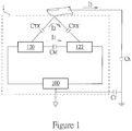
- FIG. 1 is a schematic diagram illustrating the touch operation of a mobile device 1 having a thin touchscreen.
- the thin touchscreen-based mobile device 1 is a mobile device that operates in a non-floating state, wherein the thin touchscreen-based mobile device 1 is configured to generate a current path, which is coupled to ground potential through a coupling capacitor Cf.
- the thin touchscreen-based mobile device 1 comprises a driving electrode 120, a receiving electrode 122 (also referred to as a sense electrode) and a sense circuit 100.
- the thin touchscreen-based mobile device 1 may detect the touch operation by sensing a current, i.e., I 1 , between the driving electrode and the receiving electrode.
- the sensing result of the touch signal is very sensitive to the disturbance of the current.
- the coupling capacitor Cf between the receiving electrode of the thin touchscreen-based mobile device 1 and the ground potential has a larger capacitance. Since the coupling results in the capacitive coupling effect that generates an extra current path, when a finger touches the thin touchscreen, the finger coupled to the touchscreen generates an extra current path that allows an induced current to flow to the ground via the current path, i.e., I 3 , of the human body.
- the induced current flows through the current path, i.e., I 2 , comprising the mutual capacitor C TX between the driving electrode 120 and the finger and the mutual capacitor C RX between the receiving electrode 122 and the finger, and returns to the sense circuit 100.
- the amount of current received by the sense circuit 100 increases relatively, whereas the amount of current received by the sense circuit 100 in the non-floating state reduces relatively because the thin touchscreen-based mobile device 1 is coupled to the ground.
- the variation of the amount of received current, generated by the sense circuit 100 due to the touch operation may differ between the floating state and the non-floating state of the thin touchscreen-based mobile device 1, which in turn causes a reduction in the accuracy, stability and signal-to-noise ratio of the touch sensing.
- the quality of the touch operation of the thin touchscreen-based mobile device 1 is affected by whether the thin touchscreen-based mobile device 1 is in the floating state, which may also affect the accuracy of the touch signal and degrade the user experience regarding the touch operation.
- FIG. 2 is a schematic diagram illustrating the mobile device 2 according to embodiments of the present disclosure.
- the mobile device 2 comprises a capacitive sensing system 20, a thin touchscreen 22, an isolation module 24, and a casing Fr.
- the present disclosure uses the isolation module 24 for isolating a ground voltage, so as to generate a floating ground voltage and a floating supply voltage.
- the thin touchscreen 22 is a touch panel having a thickness that is less than 400 micrometers, which is applicable in full-screen touch fingerprint recognition or a flexible screen of a mobile device.
- the thin touchscreen 22 is configured to output a mutual-capacitance sensing signal according to a touch operation of a user, and transmit the sensing signal to the capacitive sensing system 20 for recognizing the sensing signal, so as to make a judgment regarding the touch operation based on the recognition of the sensing signal.
- the thickness of the thin touchscreen 22 may refer to a thickness of a cover of the thin touchscreen 22, or a thickness of a structure between the electrode of the touch panel and a surface contacted by the touch.
- the capacitive sensing system 20 comprises a sense circuit 200 and a power supply unit 202, wherein the sense circuit 200 is coupled to the thin touchscreen 22.
- the power supply unit 202 is configured to output a supply voltage Vdd and a ground voltage Gnd, whereas the casing Fr receives the ground voltage Gnd.
- the supply voltage Vdd and the ground voltage Gnd may be referred to as a system supply voltage and a system ground voltage, respectively.
- the present invention provides an isolation module 24, which comprises an isolation circuit 240.
- the mobile device 2 can generate a floating supply voltage Vdd_f and a floating ground voltage Gnd_f are generated according to the supply voltage Vdd and the ground voltage Gnd, so as to solve the issue of the misjudgment of the touch operation.
- the voltage differences between the floating supply voltage Vdd_f and the floating ground voltage Gnd_f in the two different states are kept constant and isolated from the supply voltage Vdd and the ground voltage Gnd with the use of the voltage isolation provided by the isolation circuit 240. Consequently, the sense circuit 200 may operate stably, thereby increasing the quality of the signal detection of the touch operation of the capacitive sensing system 20.
- the thin touchscreen 22 comprises a transparent substrate Sc, at least one driving electrode 220 and at least one receiving electrode 222.
- the at least one driving electrode 220 and the at least one receiving electrode 222 are disposed on the transparent substrate Sc, and are configured to sense a touch operation performed on the thin touchscreen 22 by the user and to generate a sensing signal to be delivered to the capacitive sensing system 20.
- the driving electrode 220 and the receiving electrode 222 form a mutual-capacitance therebetween, and the value of this mutual-capacitance changes when the user touches or comes close to the thin touchscreen 22.
- the sense circuit 200 inputs a driving signal to the driving electrode 220, whereas the sensing signal received by the receiving electrode 222 is proportional to the value of the mutual-capacitance. Therefore, the value of the mutual-capacitance may be determined using the current of the sensing signal, thereby obtaining touch information. It should be noted that when a touch operation is performed and the mobile device 2 is in a non-floating state, a compensation current will be generated between the user and the driving electrode 220, wherein the compensation current will flow to the ground via the human body and then flow back to the mobile device 2 via the coupled ground.
- the compensation current will not return to the mobile device 2 via the coupled ground, such that the compensation current is received by the receiving electrode 222.
- the receiving electrode 222 receives a touch sensing signal in the floating state
- the mobile device 2 cannot make adaptive adjustment in response to a change in the signal level of the touch signal, causing the misjudgment of the touch operation. Therefore, in this case, whether the mobile device 2 is in the floating state or the non-floating state would affect the receiving electrode 222 in sensing the touch signal, thereby causing the misjudgment of the touch operation.
- the present disclosure provides the isolation circuit 240, which is coupled to the power supply unit 202 and configured to convert the supply voltage Vdd and the ground voltage Gnd, thereby providing the floating supply voltage Vdd_f and the floating ground voltage Gnd_f.
- the isolation circuit 240 may isolate the thin touchscreen 22 and the sense circuit 200 from the ground voltage Gnd, so that the thin touchscreen 22 and the sense circuit 200 are in a floating state to float with respect to the ground.
- the isolation circuit 240 is coupled to the power supply unit 202.
- the isolation circuit 240 receives the supply voltage Vdd and the ground voltage Gnd, and converts the supply voltage Vdd and the ground voltage Gnd into the floating supply voltage Vdd_f and the floating ground voltage Gnd_f, respectively.
- the isolation circuit 240 further transmits the floating supply voltage Vdd_f and the floating ground voltage Gnd_f to the thin touchscreen 22 and the sense circuit 200.
- the thin touchscreen 22 and the sense circuit 200 are not coupled to the ground directly, but isolated from the supply voltage Vdd and ground voltage Gnd through the isolation circuit 240.
- the thin touchscreen 22 and the sense circuit 200 are in the floating state, i.e. floating with respect to the ground. By maintaining the thin touchscreen 22 and the sense circuit 200 in the floating state, the quality of the signal sensing of the touch operation of the capacitive sensing system 20 is improved.
- the capacitive sensing system 20 is configured to provide the mobile device 2 a stable and isolated (with respect to the ground) floating supply voltage and floating ground voltage, so as to isolate the power supply and the ground voltage. This can ameliorate the inconsistency in the sensing current of the mobile device 2 between the floating state and the non-floating state, thereby improving the signal-to-noise ratio (SNR) of the touch sensing.
- SNR signal-to-noise ratio
- the isolation circuit 240 is a direct current-to-direct current converter (DC/DC converter), which is configured to convert the voltage value of a set of DC voltages to output another set of independent voltages, and isolate the input voltage from the output voltage.
- DC/DC converter direct current-to-direct current converter
- the isolation circuit 240 comprises an input capacitor 2400, an output capacitor 2402, a control unit 2404, and diodes 2406.
- the input capacitor 2400 is coupled between the supply voltage Vdd and the ground voltage Gnd.
- the output capacitor 2402 is coupled to the floating supply voltage Vdd_f and the floating ground voltage Gnd_f; that is, the two terminals of the output capacitor 2402 serve as output terminals of the floating supply voltage and the floating ground voltage, respectively.
- the control unit 2404 is coupled to two terminals of the input capacitor 2400.
- the diode 2406 is coupled to the floating supply voltage Vdd_f.
- the inductor 2408 is coupled between the control unit 2404 and the two diodes 2406, and is configured to perform voltage conversion. In this case, both cathodes of the two diodes 2406 are connected to one terminal of the output capacitor 2402, and are coupled to the floating supply voltage Vdd_f. Both the anodes of the two diodes 2406 are connected to the inductor 2408.
- the isolation circuit 240 regulates a voltage of an input signal via the input capacitor 2400 coupled to the supply voltage Vdd and the ground voltage Gnd, and obtains DC voltage values of the supply voltage Vdd and the ground voltage Gnd for voltage conversion.
- the control unit 2404 coupled to the input capacitor 2400, is configured to transmit a corresponding current or voltage to the inductor 2408 according to the user requirements, thereby maintaining the efficiency and voltage regulation of the system, and keeping the power of the isolation circuit within a safe range.
- the inductor 2408 coupled to control unit 2404, is configured to convert the DC voltage value and transmit the converted signal to the diode 2406 for rectification.
- the output capacitor 2402 is coupled to the diode 2406, and configured to regulate the rectified voltage, thereby generating a stable floating supply voltage Vdd_f and floating ground voltage Gnd_f.
- capacitive sensing system 20 may generate the floating supply voltage Vdd_f and the floating ground voltage Gnd_f according to the supply voltage Vdd and the ground voltage Gnd with the use of the isolation circuit 240.
- the sense circuit 200 coupled to the floating supply voltage Vdd_f and the floating ground voltage Gnd_f, may keep the thin touchscreen 22 and the sense circuit 200 in the floating state; that is, the sense circuit 200 is floating with respect to the ground. In this case, a misjudgment of the tough operation, resulting from uncoupling between the casing Fr of the mobile device 2 and the ground, will not take place, improving the quality of the sensing and user experience.
- Figure 4 is a cross-sectional view illustrating the mobile device 2 according to embodiments of the present disclosure.
- the mobile device 2 comprises the casing Fr and receives the ground voltage Gnd.
- the thin touchscreen 22, on the other hand, comprises a guard ring 224 and receives the floating ground voltage Gnd_f.
- the guard ring 224 is disposed outside of and below the thin touchscreen 22.
- the guard ring 224 is disposed outside of and below the transparent substrate Sc, and is configured to improve the stability of the potential of the transparent substrate Sc, the driving electrode 220, and the receiving electrode 222 in the thin touchscreen 22, and reduce the interference and noises received by the electrode.
- the guard ring 224 is disposed in adjacent to and in contact with the casing Fr.
- the isolation circuit 240 is used to generate the floating supply voltage Vdd_f and the floating ground voltage Gnd_f, so as to keep the thin touchscreen 22 and the sense circuit 200 in the floating state.
- the isolation module 24 further comprises an isolating material 242, which is disposed at a side surface of and below the guard ring 224.
- the isolating material 242 is disposed between the casing Fr and the guard ring 224, and is configured to isolate the ground voltage Gnd from the floating ground voltage Gnd_f. Maintaining the floating state of the floating ground voltage Gnd_f can prevent the casing Fr and the guard ring 224 from being in contact with each other, wherein the contact between the casing Fr and the guard ring 224 causes the coupling between the ground voltage Gnd and the floating ground voltage Gnd f, thereby degrading the current-based touch sensing function of the capacitive sensing system 20.
- the suitable isolating material 242 may be chosen depending on the permittivity of the material, so that the isolating material 242 can have a lower permittivity.
- the relative permittivity of the isolating material 242 i.e., a ratio of the permittivity of the material to the vacuum permittivity, can range from 1 to 4.
- the relative permittivity of the isolating material 242 can be in the range of 1 to 3, or 1 to 2.8, or 1 to 2, or 2 to 2.5, etc.
- the isolating material 242 can be used to isolate the ground voltage Gnd from the floating ground voltage Gnd_f. This prevents a direction connection between the ground voltage Gnd and the floating ground voltage Gnd_f, which results from the contact between the casing Fr and the guard ring 224. In this way, the capacitive sensing system 20 can stay in the floating state when performing the touch sensing operation, maintaining the stability of the touch operation further.
- the present disclosure is not limited to using a DC/DC converter to implement the isolation circuit 240. It is also feasible to use a voltage follower to implement the isolation circuit 240, as long as the voltage follower is capable of isolating the ground voltage Gnd from the floating ground voltage Gnd_f and generating the floating supply voltage Vdd_f according to the supply voltage Vdd. Additionally, please refer to Figure 5 , which is a schematic diagram illustrating a mobile device 5 according to another embodiment of the present disclosure.
- the capacitive sensing system 50 of the mobile device 5 further comprises a battery 5010, which is coupled between the isolation circuit 240 and the sense circuit 200.
- the battery 5010 is a backup battery for the mobile device 5 and is configured to provide backup power to the capacitive sensing system 50.
- the battery 5010 can be arranged in various manners.
- the battery 5010 may be, but is not limited to, disposed outside of the capacitive sensing system 50 or integrated into the capacitive sensing system 50. Therefore, when the power supply unit 202 fails to provide an electrical output because of insufficient power, the mobile device 5 may continue operating with the use of the battery 5010. It should be noted that when the battery power of the battery 5010 decreases and the battery power of the power supply unit 202 is sufficient, the power supply unit 202 may charge the battery 5010 via the isolation circuit 240.
- the present disclosure uses the isolation circuit and the isolating material of the isolation module to isolate the supply voltage from the ground voltage, so as to generate the floating supply voltage and the floating ground voltage.
- the reduction of the signal quality of the touch operation resulting from a difference between respective induced currents of the device in the floating state and the non-floating state, will not occur.
- the floating ground voltage can keep the ground voltage in an isolated state, so that the user may use the mobile device to perform the touch operation steadily.
- non-floating state comprises, but is not limited to, the conditions where the device is being charged or held by the hand of the user whose body has a good ground connection.
- embodiments of the present disclosure can keep the capacitive sensing system and the thin touchscreen in the floating state, so that the capacitive sensing system will not make misjudgment about the touch operation to thereby overcome the drawbacks of the prior art, wherein the misjudgment results from a difference between the induced currents of the mobile device in a floating and non-floating state.
Landscapes
- Engineering & Computer Science (AREA)
- Theoretical Computer Science (AREA)
- General Engineering & Computer Science (AREA)
- Physics & Mathematics (AREA)
- General Physics & Mathematics (AREA)
- Human Computer Interaction (AREA)
- Computer Hardware Design (AREA)
- Position Input By Displaying (AREA)
- Electronic Switches (AREA)
- Telephone Set Structure (AREA)
Abstract
Description
- The present disclosure relates to a capacitive sensing system and a mobile device, and in particular, to a capacitive sensing system applicable in a thin touchscreen and a mobile device having the thin touchscreen.
- With the advancement of technology, touch-based mobile devices have become indispensable to our daily lives. Through the touchscreen, one may use his/her finger or a stylus to operate the mobile device conveniently. To reduce the occurrence of misjudgment when the user performs multi-finger touch, most capacitive touch technologies adopt the mutual-capacitance sensing principle. Specifically, mutual-capacitance touch sensing uses a sensing panel disposed at a backside of a touchscreen panel for touch sensing. A distribution of an electromagnetic field of the touchscreen varies according to a position at which a user touches, thus causing a change in the mutual-capacitance between electrodes of the sensing panel. As a result, the sensing panel may determine the user's touch operation by detecting a variation of a current flowing through the electrodes.
- However, it should be noted that many mobile devices adopt a thinner touchscreen, such as a touch panel having a thinner cover layer (i.e., a thin cover). When the user performs a touch operation, such thinner touchscreen may have a greater induced capacitance between the electrode of the sensing panel and the human body. In these cases, when the mobile device is in a non-floating state (i.e., a grounding state), a larger portion of an induced current generated between the user and the detection electrode will be directed to the ground via the human body, instead of flowing to the detection electrode, because the mobile device is in the non-floating state. Therefore, when the detection electrode receives the current in the non-floating state, the amount of induced current received by the detection electrode is less than that received by the detection electrode in the floating state, resulting in an increase in the proportion of the noise voltage in the induced current. Briefly, the amount of induced current of the mobile device having a thin touchscreen is different from that of the mobile device in the non-floating state. However, the host or the system determines whether a touch has taken place in accordance with the sensed amount of induced current and a pre-stored reference amount, wherein the reference amount is relatively constant and will not change in response to whether the mobile device is in the floating or non-floating states. Thus, the determination of the touch operation in one of the floating state or the non-floating state will be inaccurate, resulting in misjudgment of the touch operation.
- In view of the foregoing, there is a need for improvement in the related art.
- Therefore, a main object of some embodiments of the present disclosure is to provide a capacitive sensing system applicable in a mobile device, which is used for resolving the issue of different amounts of induced current of the mobile device in the floating state and non-floating state, so as to overcome the drawbacks of the prior art.
- In order to resolve the above issues, the present disclosure provides a mobile device. The mobile device comprises a casing, configured to accommodate or support the mobile device; a thin touchscreen, comprising at least one driving electrode and at least one receiving electrode, wherein the driving electrode is configured to receive a driving signal, and the receiving electrode is configured to generate a sensing signal to sense a touch operation; a capacitive sensing system, comprising a sense circuit, coupled to the at least one receiving electrode and configured to generate the driving signal and receive the sensing signal to determine the touch operation, and a power supply unit, configured to output a supply voltage and a ground voltage; and an isolation module, configured to isolate the supply voltage and the ground voltage.
- For instance, the casing receives the ground voltage.
- For instance, the thin touchscreen has a thickness less than 400 micrometers.
- For instance, the thin touchscreen is further configured to perform full-screen fingerprint recognition.
- For instance, the thin touchscreen is a flexible screen.
- For instance, the isolation module comprises an isolation circuit, coupled to the power supply unit and configured to generate a floating supply voltage and a floating ground voltage according to the supply voltage and the ground voltage. The floating supply voltage and the floating ground voltage are isolated from the supply voltage and the ground voltage, wherein the sense circuit receives the floating supply voltage and the floating ground voltage to stay in a floating state to float with respect to the ground voltage.
- For instance, the thin touchscreen receives the floating supply voltage and the floating ground voltage to stay in the floating state to float with respect to the ground voltage.
- For instance, a voltage difference between the floating supply voltage and the floating ground voltage is a fixed value.
- For instance, the isolation circuit is a direct current to direct current (DC/DC) converter, configured to receive the supply voltage and the ground voltage to generate the floating supply voltage and the floating ground voltage. The DC/DC converter comprises: an input capacitor, coupled between the supply voltage and the ground voltage; an output capacitor, coupled between the floating supply voltage and the floating ground voltage; a control unit, coupled to the input capacitor; an inductor, coupled between the control unit and the output capacitor, and configured to perform a voltage conversion operation; and a rectifier assembly, coupled between the inductor and the output capacitor.
- For instance, the thin touchscreen further comprises a transparent substrate, wherein the driving electrode and the receiving electrode are disposed on the transparent substrate; and a guard ring, disposed adjacent to the transparent substrate and connected to the floating ground voltage.
- For instance, the mobile device further comprises an isolating material, wherein the casing is configured to accommodate the thin touchscreen and is connected to the ground voltage, and the isolating material is disposed between the guard ring and the casing to isolate the guard ring from the casing.
- For instance, the isolating material has a relative permittivity ranging from 1 to 3, 1 to 2, 2 to 3, or 1 to 2.8.
- The present disclosure further provides a capacitive sensing system. The capacitive sensing system comprises a sense circuit, coupled to a capacitor array, and configured to generate a driving signal to the capacitor array, and receive a sensing signal from the capacitor array to determine a touch operation; a power supply unit, configured to output a supply voltage and a ground voltage; and an isolation module, configured to isolate the supply voltage and the ground voltage from the sense circuit.
- For instance, the isolation module generates a floating supply voltage and a floating ground voltage according to the supply voltage and the ground voltage, and provides the floating supply voltage and floating ground voltage to the sense circuit to isolate the supply voltage and the ground voltage.
- For instance, a voltage difference between the floating supply voltage and the floating ground voltage is a fixed value.
- For instance, the isolation module comprises a DC/DC converter, configured to receive the supply voltage and the ground voltage to generate the floating supply voltage and the floating ground voltage. The DC/DC converter comprises an input capacitor, coupled between the supply voltage and the ground voltage; an output capacitor, coupled between the floating supply voltage and the floating ground voltage; a control unit, coupled to the input capacitor; an inductor, coupled between the control unit and the output capacitor, and configured to perform a voltage conversion operation; and a rectifier assembly, coupled between the inductor and the output capacitor.
- For instance, the capacitor array is disposed on a thin touchscreen, and the isolation module further provides the floating supply voltage and floating ground voltage to the thin touchscreen.
- For instance, the capacitor array is disposed on a whole screen of a thin touchscreen and configured to perform fingerprint recognition.
-
-
Figure 1 is a schematic diagram illustrating the touch operation of a thin touchscreen-based mobile device. -
Figure 2 is a schematic diagram illustrating a mobile device according to embodiments of the present disclosure; -
Figure 3 is a schematic diagram illustrating an isolation circuit according to embodiments of the present disclosure; -
Figure 4 is a cross-sectional view illustrating a mobile device according to embodiments of the present disclosure; -
Figure 5 is a schematic diagram illustrating a mobile device according to embodiments of the present disclosure. - The detailed description provided below in connection with the appended drawings is intended as a description of the present examples so that so that those skilled in the art may better understand the purposes, technical solutions, and advantages of the present application. It should be noted that the embodiments of the present application are provided for illustrative purposes, and are not limiting.
- Reference is made to
Figure 1 , which is a schematic diagram illustrating the touch operation of amobile device 1 having a thin touchscreen. As shown inFigure 1 , the thin touchscreen-basedmobile device 1 is a mobile device that operates in a non-floating state, wherein the thin touchscreen-basedmobile device 1 is configured to generate a current path, which is coupled to ground potential through a coupling capacitor Cf. The thin touchscreen-basedmobile device 1 comprises adriving electrode 120, a receiving electrode 122 (also referred to as a sense electrode) and asense circuit 100. When the user performs a touch operation via the thin touchscreen-basedmobile device 1, the thin touchscreen-basedmobile device 1 may detect the touch operation by sensing a current, i.e., I1, between the driving electrode and the receiving electrode. It should be noted that since the touchscreen of the thin touchscreen-basedmobile device 1 is quite thin, the sensing result of the touch signal is very sensitive to the disturbance of the current. Specifically, when themobile device 1 is in the non-floating state, that is, the thin touchscreen-basedmobile device 1 is coupled to the ground potential, the coupling capacitor Cf between the receiving electrode of the thin touchscreen-basedmobile device 1 and the ground potential has a larger capacitance. Since the coupling results in the capacitive coupling effect that generates an extra current path, when a finger touches the thin touchscreen, the finger coupled to the touchscreen generates an extra current path that allows an induced current to flow to the ground via the current path, i.e., I3, of the human body. - In this way, as compared with the situation in which the
mobile device 100 is in a floating state, the induced current flows through the current path, i.e., I2, comprising the mutual capacitor CTX between thedriving electrode 120 and the finger and the mutual capacitor CRX between thereceiving electrode 122 and the finger, and returns to thesense circuit 100. The amount of current received by thesense circuit 100 increases relatively, whereas the amount of current received by thesense circuit 100 in the non-floating state reduces relatively because the thin touchscreen-basedmobile device 1 is coupled to the ground. As a result, the variation of the amount of received current, generated by thesense circuit 100 due to the touch operation, may differ between the floating state and the non-floating state of the thin touchscreen-basedmobile device 1, which in turn causes a reduction in the accuracy, stability and signal-to-noise ratio of the touch sensing. Briefly, the quality of the touch operation of the thin touchscreen-basedmobile device 1 is affected by whether the thin touchscreen-basedmobile device 1 is in the floating state, which may also affect the accuracy of the touch signal and degrade the user experience regarding the touch operation. - Therefore, the present disclosure provides a
mobile device 2. Please refer toFigure 2 , which is a schematic diagram illustrating themobile device 2 according to embodiments of the present disclosure. Themobile device 2 comprises acapacitive sensing system 20, athin touchscreen 22, an isolation module 24, and a casing Fr. The present disclosure uses the isolation module 24 for isolating a ground voltage, so as to generate a floating ground voltage and a floating supply voltage. Thethin touchscreen 22 is a touch panel having a thickness that is less than 400 micrometers, which is applicable in full-screen touch fingerprint recognition or a flexible screen of a mobile device. Thethin touchscreen 22 is configured to output a mutual-capacitance sensing signal according to a touch operation of a user, and transmit the sensing signal to thecapacitive sensing system 20 for recognizing the sensing signal, so as to make a judgment regarding the touch operation based on the recognition of the sensing signal. As used herein, the thickness of thethin touchscreen 22 may refer to a thickness of a cover of thethin touchscreen 22, or a thickness of a structure between the electrode of the touch panel and a surface contacted by the touch. Thecapacitive sensing system 20 comprises asense circuit 200 and apower supply unit 202, wherein thesense circuit 200 is coupled to thethin touchscreen 22. Thepower supply unit 202 is configured to output a supply voltage Vdd and a ground voltage Gnd, whereas the casing Fr receives the ground voltage Gnd. In this case, the supply voltage Vdd and the ground voltage Gnd may be referred to as a system supply voltage and a system ground voltage, respectively. In order to address the issue where a misjudgment of the touch operation may arise because themobile device 2 may be in a floating or non-floating state, the present invention provides an isolation module 24, which comprises anisolation circuit 240. By using theisolation circuit 240 coupled to thepower supply unit 202, themobile device 2 can generate a floating supply voltage Vdd_f and a floating ground voltage Gnd_f are generated according to the supply voltage Vdd and the ground voltage Gnd, so as to solve the issue of the misjudgment of the touch operation. In this way, no matter whether themobile device 2 is in the floating state or non-floating state, the voltage differences between the floating supply voltage Vdd_f and the floating ground voltage Gnd_f in the two different states are kept constant and isolated from the supply voltage Vdd and the ground voltage Gnd with the use of the voltage isolation provided by theisolation circuit 240. Consequently, thesense circuit 200 may operate stably, thereby increasing the quality of the signal detection of the touch operation of thecapacitive sensing system 20. - In one embodiment, the
thin touchscreen 22 comprises a transparent substrate Sc, at least one drivingelectrode 220 and at least one receivingelectrode 222. The at least one drivingelectrode 220 and the at least one receivingelectrode 222 are disposed on the transparent substrate Sc, and are configured to sense a touch operation performed on thethin touchscreen 22 by the user and to generate a sensing signal to be delivered to thecapacitive sensing system 20. In this case, the drivingelectrode 220 and the receivingelectrode 222 form a mutual-capacitance therebetween, and the value of this mutual-capacitance changes when the user touches or comes close to thethin touchscreen 22. In this case, thesense circuit 200 inputs a driving signal to the drivingelectrode 220, whereas the sensing signal received by the receivingelectrode 222 is proportional to the value of the mutual-capacitance. Therefore, the value of the mutual-capacitance may be determined using the current of the sensing signal, thereby obtaining touch information. It should be noted that when a touch operation is performed and themobile device 2 is in a non-floating state, a compensation current will be generated between the user and the drivingelectrode 220, wherein the compensation current will flow to the ground via the human body and then flow back to themobile device 2 via the coupled ground. When a touch operation is performed and themobile device 2 is in a floating state, the compensation current will not return to themobile device 2 via the coupled ground, such that the compensation current is received by the receivingelectrode 222. As a result, when the receivingelectrode 222 receives a touch sensing signal in the floating state, themobile device 2 cannot make adaptive adjustment in response to a change in the signal level of the touch signal, causing the misjudgment of the touch operation. Therefore, in this case, whether themobile device 2 is in the floating state or the non-floating state would affect the receivingelectrode 222 in sensing the touch signal, thereby causing the misjudgment of the touch operation. - Hence, the present disclosure provides the
isolation circuit 240, which is coupled to thepower supply unit 202 and configured to convert the supply voltage Vdd and the ground voltage Gnd, thereby providing the floating supply voltage Vdd_f and the floating ground voltage Gnd_f. It should be noted that theisolation circuit 240 may isolate thethin touchscreen 22 and thesense circuit 200 from the ground voltage Gnd, so that thethin touchscreen 22 and thesense circuit 200 are in a floating state to float with respect to the ground. Specifically, theisolation circuit 240 is coupled to thepower supply unit 202. Theisolation circuit 240 receives the supply voltage Vdd and the ground voltage Gnd, and converts the supply voltage Vdd and the ground voltage Gnd into the floating supply voltage Vdd_f and the floating ground voltage Gnd_f, respectively. Moreover, theisolation circuit 240 further transmits the floating supply voltage Vdd_f and the floating ground voltage Gnd_f to thethin touchscreen 22 and thesense circuit 200. As a result, thethin touchscreen 22 and thesense circuit 200 are not coupled to the ground directly, but isolated from the supply voltage Vdd and ground voltage Gnd through theisolation circuit 240. Thethin touchscreen 22 and thesense circuit 200 are in the floating state, i.e. floating with respect to the ground. By maintaining thethin touchscreen 22 and thesense circuit 200 in the floating state, the quality of the signal sensing of the touch operation of thecapacitive sensing system 20 is improved. - In other words, during the touch operation, the
capacitive sensing system 20 is configured to provide the mobile device 2 a stable and isolated (with respect to the ground) floating supply voltage and floating ground voltage, so as to isolate the power supply and the ground voltage. This can ameliorate the inconsistency in the sensing current of themobile device 2 between the floating state and the non-floating state, thereby improving the signal-to-noise ratio (SNR) of the touch sensing. - Specifically, please refer to
Figure 3 , which is a schematic diagram illustrating anisolation circuit 240 according to embodiments of the present disclosure. In this example, theisolation circuit 240 is a direct current-to-direct current converter (DC/DC converter), which is configured to convert the voltage value of a set of DC voltages to output another set of independent voltages, and isolate the input voltage from the output voltage. In one embodiment, theisolation circuit 240 comprises aninput capacitor 2400, anoutput capacitor 2402, acontrol unit 2404, anddiodes 2406. Theinput capacitor 2400 is coupled between the supply voltage Vdd and the ground voltage Gnd. Theoutput capacitor 2402 is coupled to the floating supply voltage Vdd_f and the floating ground voltage Gnd_f; that is, the two terminals of theoutput capacitor 2402 serve as output terminals of the floating supply voltage and the floating ground voltage, respectively. Thecontrol unit 2404 is coupled to two terminals of theinput capacitor 2400. Thediode 2406 is coupled to the floating supply voltage Vdd_f. Theinductor 2408 is coupled between thecontrol unit 2404 and the twodiodes 2406, and is configured to perform voltage conversion. In this case, both cathodes of the twodiodes 2406 are connected to one terminal of theoutput capacitor 2402, and are coupled to the floating supply voltage Vdd_f. Both the anodes of the twodiodes 2406 are connected to theinductor 2408. Hence, theisolation circuit 240 regulates a voltage of an input signal via theinput capacitor 2400 coupled to the supply voltage Vdd and the ground voltage Gnd, and obtains DC voltage values of the supply voltage Vdd and the ground voltage Gnd for voltage conversion. Thecontrol unit 2404, coupled to theinput capacitor 2400, is configured to transmit a corresponding current or voltage to theinductor 2408 according to the user requirements, thereby maintaining the efficiency and voltage regulation of the system, and keeping the power of the isolation circuit within a safe range. Theinductor 2408, coupled to controlunit 2404, is configured to convert the DC voltage value and transmit the converted signal to thediode 2406 for rectification. Theoutput capacitor 2402 is coupled to thediode 2406, and configured to regulate the rectified voltage, thereby generating a stable floating supply voltage Vdd_f and floating ground voltage Gnd_f. - Hence,
capacitive sensing system 20 may generate the floating supply voltage Vdd_f and the floating ground voltage Gnd_f according to the supply voltage Vdd and the ground voltage Gnd with the use of theisolation circuit 240. It should be noted that thesense circuit 200, coupled to the floating supply voltage Vdd_f and the floating ground voltage Gnd_f, may keep thethin touchscreen 22 and thesense circuit 200 in the floating state; that is, thesense circuit 200 is floating with respect to the ground. In this case, a misjudgment of the tough operation, resulting from uncoupling between the casing Fr of themobile device 2 and the ground, will not take place, improving the quality of the sensing and user experience. - Additionally, please refer to
Figure 4 , which is a cross-sectional view illustrating themobile device 2 according to embodiments of the present disclosure. As shown inFigure 4 , themobile device 2 comprises the casing Fr and receives the ground voltage Gnd. Thethin touchscreen 22, on the other hand, comprises aguard ring 224 and receives the floating ground voltage Gnd_f. It should be noted that theguard ring 224 is disposed outside of and below thethin touchscreen 22. Specifically, theguard ring 224 is disposed outside of and below the transparent substrate Sc, and is configured to improve the stability of the potential of the transparent substrate Sc, the drivingelectrode 220, and the receivingelectrode 222 in thethin touchscreen 22, and reduce the interference and noises received by the electrode. Hence, in general, theguard ring 224 is disposed in adjacent to and in contact with the casing Fr. However, in the present disclosure, theisolation circuit 240 is used to generate the floating supply voltage Vdd_f and the floating ground voltage Gnd_f, so as to keep thethin touchscreen 22 and thesense circuit 200 in the floating state. To further keep thethin touchscreen 22 in the floating state such that a situation where thethin touchscreen 22 receives the ground voltage Gnd because of the contact between theguard ring 224 and the casing Fr will not occur, the isolation module 24 further comprises an isolatingmaterial 242, which is disposed at a side surface of and below theguard ring 224. The isolatingmaterial 242 is disposed between the casing Fr and theguard ring 224, and is configured to isolate the ground voltage Gnd from the floating ground voltage Gnd_f. Maintaining the floating state of the floating ground voltage Gnd_f can prevent the casing Fr and theguard ring 224 from being in contact with each other, wherein the contact between the casing Fr and theguard ring 224 causes the coupling between the ground voltage Gnd and the floating ground voltage Gnd f, thereby degrading the current-based touch sensing function of thecapacitive sensing system 20. - Specifically, to prevent the isolating
material 242 from transmitting the voltage, the suitable isolatingmaterial 242 may be chosen depending on the permittivity of the material, so that the isolatingmaterial 242 can have a lower permittivity. For example, the relative permittivity of the isolatingmaterial 242, i.e., a ratio of the permittivity of the material to the vacuum permittivity, can range from 1 to 4. Preferably, the relative permittivity of the isolatingmaterial 242 can be in the range of 1 to 3, or 1 to 2.8, or 1 to 2, or 2 to 2.5, etc. In other words, when an external electric field is applied to the isolatingmaterial 242, it is more difficult to polarize the isolatingmaterial 242. As a result, it is difficult for the external electric field to transmit an electric field via the isolatingmaterial 242, thus effectively isolating the ground voltage Gnd coupled to the casing Fr from the floating ground voltage Gnd_f coupled to theguard ring 224. - Therefore, by disposing the isolating
material 242 at the lateral side of and below thecapacitive sensing system 20, and between the casing Fr and theguard ring 224, the isolatingmaterial 242 can be used to isolate the ground voltage Gnd from the floating ground voltage Gnd_f. This prevents a direction connection between the ground voltage Gnd and the floating ground voltage Gnd_f, which results from the contact between the casing Fr and theguard ring 224. In this way, thecapacitive sensing system 20 can stay in the floating state when performing the touch sensing operation, maintaining the stability of the touch operation further. - It should be noted that the foregoing embodiments are provided for the purpose of explaining the ideas and principles of the present disclosure, and persons having ordinary skill in the art may make various modifications thereto. For example, the present disclosure is not limited to using a DC/DC converter to implement the
isolation circuit 240. It is also feasible to use a voltage follower to implement theisolation circuit 240, as long as the voltage follower is capable of isolating the ground voltage Gnd from the floating ground voltage Gnd_f and generating the floating supply voltage Vdd_f according to the supply voltage Vdd. Additionally, please refer toFigure 5 , which is a schematic diagram illustrating amobile device 5 according to another embodiment of the present disclosure. Themobile device 5 is similar to themobile device 2, and hence, the same reference numerals are used to indicate the same components. As shown in theFigure 5 , thecapacitive sensing system 50 of themobile device 5 further comprises abattery 5010, which is coupled between theisolation circuit 240 and thesense circuit 200. Thebattery 5010 is a backup battery for themobile device 5 and is configured to provide backup power to thecapacitive sensing system 50. Thebattery 5010 can be arranged in various manners. For example, thebattery 5010 may be, but is not limited to, disposed outside of thecapacitive sensing system 50 or integrated into thecapacitive sensing system 50. Therefore, when thepower supply unit 202 fails to provide an electrical output because of insufficient power, themobile device 5 may continue operating with the use of thebattery 5010. It should be noted that when the battery power of thebattery 5010 decreases and the battery power of thepower supply unit 202 is sufficient, thepower supply unit 202 may charge thebattery 5010 via theisolation circuit 240. - In view of the foregoing, the present disclosure uses the isolation circuit and the isolating material of the isolation module to isolate the supply voltage from the ground voltage, so as to generate the floating supply voltage and the floating ground voltage. In this way, when the user performs a touch operation on the thin touchscreen, the reduction of the signal quality of the touch operation, resulting from a difference between respective induced currents of the device in the floating state and the non-floating state, will not occur. The floating ground voltage can keep the ground voltage in an isolated state, so that the user may use the mobile device to perform the touch operation steadily.
- As used herein, the phrase "non-floating state" comprises, but is not limited to, the conditions where the device is being charged or held by the hand of the user whose body has a good ground connection.
- In view of the foregoing, as compared to the conventional art, embodiments of the present disclosure can keep the capacitive sensing system and the thin touchscreen in the floating state, so that the capacitive sensing system will not make misjudgment about the touch operation to thereby overcome the drawbacks of the prior art, wherein the misjudgment results from a difference between the induced currents of the mobile device in a floating and non-floating state.
Claims (18)
- A mobile device, comprising:a casing, configured to accommodate or support the mobile device;a thin touchscreen, comprising at least one driving electrode and at least one receiving electrode, wherein the driving electrode is configured to receive a driving signal, and the receiving electrode is configured to generate a sensing signal to sense a touch operation;a capacitive sensing system, comprising:a sense circuit, coupled to the at least one receiving electrode, and configured to generate the driving signal and receive the sensing signal to determine the touch operation; anda power supply unit, configured to output a supply voltage and a ground voltage; andan isolation module, configured to isolate the supply voltage and the ground voltage.
- The mobile device of claim 1, wherein the casing receives the ground voltage.
- The mobile device of claim 1, wherein the thin touchscreen has a thickness less than 400 micrometers.
- The mobile device of claim 1, wherein the thin touchscreen is further configured to perform full-screen fingerprint recognition.
- The mobile device of claim 1, wherein the thin touchscreen is a flexible screen.
- The mobile device of any of claims 1 to 5, wherein the isolation module comprises:an isolation circuit, coupled to the power supply unit, and configured to generate a floating supply voltage and a floating ground voltage according to the supply voltage and the ground voltage, the floating supply voltage and the floating ground voltage being isolated from the supply voltage and the ground voltage;wherein the sense circuit receives the floating supply voltage and the floating ground voltage to stay in a floating state to float with respect to the ground voltage.
- The mobile device of claim 6, wherein the thin touchscreen receives the floating supply voltage and the floating ground voltage to stay in the floating state to float with respect to the ground voltage.
- The mobile device of claim 6, wherein a voltage difference between the floating supply voltage and the floating ground voltage is a fixed value.
- The mobile device of claim 6, wherein the isolation circuit is a direct current to direct current (DC/DC) converter, configured to receive the supply voltage and the ground voltage to generate the floating supply voltage and the floating ground voltage; the DC/DC converter comprises:an input capacitor, coupled between the supply voltage and the ground voltage;an output capacitor, coupled between the floating supply voltage and the floating ground voltage;a control unit, coupled to the input capacitor;an inductor, coupled between the control unit and the output capacitor, and configured to perform a voltage conversion operation; anda rectifier assembly, coupled between the inductor and the output capacitor.
- The mobile device of any of claims 6 to 9, wherein the thin touchscreen further comprises:a transparent substrate, wherein the driving electrode and the receiving electrode are disposed on the transparent substrate; anda guard ring, disposed adjacent to the transparent substrate and connected to the floating ground voltage.
- The mobile device of claim 10, further comprising an isolating material, wherein the casing is configured to accommodate the thin touchscreen and is connected to the ground voltage, and the isolating material is disposed between the guard ring and the casing to isolate the guard ring from the casing.
- The mobile device of claim 11, wherein the isolating material has a relative permittivity ranging from 1 to 3, 1 to 2, 2 to 3, or 1 to 2.8.
- A capacitive sensing system, comprising:a sense circuit, coupled to a capacitor array, and configured to generate a driving signal to the capacitor array, and receive a sensing signal from the capacitor array to determine a touch operation;a power supply unit, configured to output a supply voltage and a ground voltage; andan isolation module, configured to isolate the supply voltage and the ground voltage from the sense circuit.
- The capacitive sensing system of claim 13, wherein the isolation module generates a floating supply voltage and a floating ground voltage according to the supply voltage and the ground voltage, and provides the floating supply voltage and floating ground voltage to the sense circuit to isolate the supply voltage and the ground voltage.
- The capacitive sensing system of claim 14, wherein a voltage difference between the floating supply voltage and the floating ground voltage is a fixed value.
- The capacitive sensing system of claim 14, wherein the isolation module comprises a DC/DC converter, configured to receive the supply voltage and the ground voltage to generate the floating supply voltage and the floating ground voltage; and the DC/DC converter comprises:an input capacitor, coupled between the supply voltage and the ground voltage;an output capacitor, coupled between the floating supply voltage and the floating ground voltage;a control unit, coupled to the input capacitor;an inductor, coupled between the control unit and the output capacitor, and configured to perform a voltage conversion operation; anda rectifier assembly, coupled between the inductor and the output capacitor.
- The capacitive sensing system of claim 14, wherein the capacitor array is disposed on a thin touchscreen, and the isolation module further provides the floating supply voltage and floating ground voltage to the thin touchscreen.
- The capacitive sensing system of any of claims 13 to 16, wherein the capacitor array is disposed on a whole screen of a thin touchscreen and configured to perform fingerprint recognition.
Applications Claiming Priority (1)
| Application Number | Priority Date | Filing Date | Title |
|---|---|---|---|
| PCT/CN2017/112867 WO2019100328A1 (en) | 2017-11-24 | 2017-11-24 | Capacitance sensing system and mobile device |
Publications (3)
| Publication Number | Publication Date |
|---|---|
| EP3537267A1 true EP3537267A1 (en) | 2019-09-11 |
| EP3537267A4 EP3537267A4 (en) | 2019-12-04 |
| EP3537267B1 EP3537267B1 (en) | 2023-06-28 |
Family
ID=66631257
Family Applications (1)
| Application Number | Title | Priority Date | Filing Date |
|---|---|---|---|
| EP17911397.2A Active EP3537267B1 (en) | 2017-11-24 | 2017-11-24 | Capacitance sensing system and mobile device |
Country Status (4)
| Country | Link |
|---|---|
| US (1) | US10969886B2 (en) |
| EP (1) | EP3537267B1 (en) |
| CN (1) | CN110100223B (en) |
| WO (1) | WO2019100328A1 (en) |
Cited By (1)
| Publication number | Priority date | Publication date | Assignee | Title |
|---|---|---|---|---|
| WO2022068571A1 (en) * | 2020-09-30 | 2022-04-07 | 华为技术有限公司 | Electronic device and control method therefor, touch system, and chip system |
Families Citing this family (2)
| Publication number | Priority date | Publication date | Assignee | Title |
|---|---|---|---|---|
| JP2021163393A (en) * | 2020-04-03 | 2021-10-11 | シャープ株式会社 | Display device |
| CN114327114B (en) * | 2020-09-30 | 2023-10-20 | 华为技术有限公司 | An electronic device and its control method, touch system, and chip system |
Family Cites Families (20)
| Publication number | Priority date | Publication date | Assignee | Title |
|---|---|---|---|---|
| US5754413A (en) * | 1996-02-23 | 1998-05-19 | Lucent Technologies Inc. | Reduced voltage stress asymmetrical DC-to-DC converter using first and second transformers having differing turns ratios |
| US6021499A (en) * | 1998-03-31 | 2000-02-01 | Sony Corporation Of Japan | Isolated ground reference DC power supply |
| US6765810B2 (en) * | 2002-08-02 | 2004-07-20 | Artesyn Technologies, Inc. | Full-wave coupled inductor power converter having synchronous rectifiers and two input switches that are simultaneously off for a time period of each switching cycle |
| KR20070075583A (en) * | 2006-01-13 | 2007-07-24 | 삼성전자주식회사 | Liquid crystal display |
| US7796123B1 (en) * | 2006-06-20 | 2010-09-14 | Eastman Kodak Company | Touchscreen with carbon nanotube conductive layers |
| KR101557126B1 (en) * | 2008-07-16 | 2015-10-05 | 삼성디스플레이 주식회사 | Touch sensor and liquid crystal display having the same |
| JP5337061B2 (en) * | 2009-02-20 | 2013-11-06 | セイコーインスツル株式会社 | Touch panel and display device including the same |
| FR2949008B1 (en) * | 2009-08-07 | 2011-09-16 | Nanotec Solution | CAPACITIVE DETECTION DEVICE WITH FUNCTION INTEGRATION. |
| JP5346769B2 (en) * | 2009-10-21 | 2013-11-20 | 株式会社ジャパンディスプレイ | Touch panel and display device including the same |
| KR20120133848A (en) * | 2011-06-01 | 2012-12-11 | 삼성디스플레이 주식회사 | flexible touch screen panel |
| KR101356968B1 (en) * | 2012-06-14 | 2014-02-03 | 엘지디스플레이 주식회사 | Display device with integrated touch screen |
| KR101349665B1 (en) * | 2012-06-14 | 2014-01-10 | 엘지디스플레이 주식회사 | Display device with integrated touch screen |
| JP6345029B2 (en) * | 2014-08-11 | 2018-06-20 | 三菱電機株式会社 | Touch screen, touch panel, display device, and electronic device |
| US10191597B2 (en) * | 2015-06-30 | 2019-01-29 | Synaptics Incorporated | Modulating a reference voltage to preform capacitive sensing |
| JP6765807B2 (en) * | 2015-01-05 | 2020-10-07 | シナプティクス インコーポレイテッド | Modulation of reference voltage for capacitive sensing |
| CN106293277B (en) * | 2015-05-11 | 2019-08-30 | 上海和辉光电有限公司 | Full screen fingerprinting method and structure |
| GB2543340B (en) * | 2015-10-16 | 2019-09-04 | Touchnetix Ltd | Capacitive sensor apparatus and methods |
| CN105184287B (en) * | 2015-10-29 | 2019-10-01 | 京东方科技集团股份有限公司 | A kind of electrode structure, fingerprint recognition mould group and preparation method thereof, display device |
| KR102714659B1 (en) * | 2016-12-09 | 2024-10-07 | 엘지디스플레이 주식회사 | Electronic device |
| CN107223230A (en) * | 2017-05-05 | 2017-09-29 | 深圳市汇顶科技股份有限公司 | The touch control method of capacitance touch-control device, capacitance plate and capacitance plate |
-
2017
- 2017-11-24 EP EP17911397.2A patent/EP3537267B1/en active Active
- 2017-11-24 CN CN201780001866.6A patent/CN110100223B/en active Active
- 2017-11-24 WO PCT/CN2017/112867 patent/WO2019100328A1/en not_active Ceased
-
2018
- 2018-12-03 US US16/207,827 patent/US10969886B2/en not_active Expired - Fee Related
Cited By (2)
| Publication number | Priority date | Publication date | Assignee | Title |
|---|---|---|---|---|
| WO2022068571A1 (en) * | 2020-09-30 | 2022-04-07 | 华为技术有限公司 | Electronic device and control method therefor, touch system, and chip system |
| CN114327115A (en) * | 2020-09-30 | 2022-04-12 | 华为技术有限公司 | Electronic equipment and control method thereof, touch system and chip system |
Also Published As
| Publication number | Publication date |
|---|---|
| US10969886B2 (en) | 2021-04-06 |
| WO2019100328A1 (en) | 2019-05-31 |
| CN110100223B (en) | 2022-09-13 |
| US20190163305A1 (en) | 2019-05-30 |
| CN110100223A (en) | 2019-08-06 |
| EP3537267A4 (en) | 2019-12-04 |
| EP3537267B1 (en) | 2023-06-28 |
Similar Documents
| Publication | Publication Date | Title |
|---|---|---|
| US9519363B2 (en) | Stylus and stylus circuitry for capacitive touch screens | |
| US8063330B2 (en) | Uniform threshold for capacitive sensing | |
| US8773405B1 (en) | Stylus and related human interface devices with dynamic power control circuits | |
| US10969886B2 (en) | Capacitive sensing system and mobile device | |
| CN104603728B (en) | capacitance measurement | |
| US11157712B2 (en) | Fingerprint recognition driving circuit, fingerprint recognition module, touch screen, display device and fingerprint recognition driving method | |
| JP6153042B2 (en) | Touch sensing system and display device | |
| KR102255080B1 (en) | Modulating a reference voltage to perform capacitive sensing | |
| US10254896B2 (en) | Display with case electrically connected to ground | |
| US20170285771A1 (en) | Active stylus pen and touch sensing system including the same | |
| WO2016112848A1 (en) | Electronic device and touch sensing system thereof, and detection method for touch sensing system | |
| CN112051933B (en) | Touch detection circuit, input device, and electronic apparatus | |
| CN102023739A (en) | touch device | |
| JP2020086743A (en) | Touch detection circuit, input device, and electronic device | |
| US20100066679A1 (en) | Power saving apparatus and method for wireless mouse | |
| US12092671B2 (en) | Capacitance measurement apparatus | |
| CN109150155A (en) | Advanced capacitive proximity sensor | |
| US12260047B2 (en) | Touch sensing device and touch sensing method | |
| US10684732B2 (en) | Capacitive sensor apparatus and methods | |
| US20120139560A1 (en) | Touch apparatus | |
| CN108780371B (en) | Touch system and its power supply circuit | |
| CN223540544U (en) | A touch detection circuit composed of discrete components | |
| WO2017079912A1 (en) | Fingerprint recognition system | |
| JP2001178136A (en) | Power supply circuit for electrostatic capacity sensor circuit | |
| KR101460104B1 (en) | Method for Driving an Electronic Device having A Touch Panel |
Legal Events
| Date | Code | Title | Description |
|---|---|---|---|
| STAA | Information on the status of an ep patent application or granted ep patent |
Free format text: STATUS: UNKNOWN |
|
| STAA | Information on the status of an ep patent application or granted ep patent |
Free format text: STATUS: THE INTERNATIONAL PUBLICATION HAS BEEN MADE |
|
| PUAI | Public reference made under article 153(3) epc to a published international application that has entered the european phase |
Free format text: ORIGINAL CODE: 0009012 |
|
| STAA | Information on the status of an ep patent application or granted ep patent |
Free format text: STATUS: REQUEST FOR EXAMINATION WAS MADE |
|
| 17P | Request for examination filed |
Effective date: 20181205 |
|
| AK | Designated contracting states |
Kind code of ref document: A1 Designated state(s): AL AT BE BG CH CY CZ DE DK EE ES FI FR GB GR HR HU IE IS IT LI LT LU LV MC MK MT NL NO PL PT RO RS SE SI SK SM TR |
|
| AX | Request for extension of the european patent |
Extension state: BA ME |
|
| R17P | Request for examination filed (corrected) |
Effective date: 20181205 |
|
| A4 | Supplementary search report drawn up and despatched |
Effective date: 20191107 |
|
| RIC1 | Information provided on ipc code assigned before grant |
Ipc: G06F 1/26 20060101ALI20191031BHEP Ipc: G06F 3/041 20060101AFI20191031BHEP |
|
| STAA | Information on the status of an ep patent application or granted ep patent |
Free format text: STATUS: EXAMINATION IS IN PROGRESS |
|
| 17Q | First examination report despatched |
Effective date: 20201112 |
|
| DAV | Request for validation of the european patent (deleted) | ||
| DAX | Request for extension of the european patent (deleted) | ||
| GRAP | Despatch of communication of intention to grant a patent |
Free format text: ORIGINAL CODE: EPIDOSNIGR1 |
|
| STAA | Information on the status of an ep patent application or granted ep patent |
Free format text: STATUS: GRANT OF PATENT IS INTENDED |
|
| RIC1 | Information provided on ipc code assigned before grant |
Ipc: G06F 1/16 20060101ALN20230322BHEP Ipc: G06F 1/26 20060101ALI20230322BHEP Ipc: G06F 3/041 20060101AFI20230322BHEP |
|
| INTG | Intention to grant announced |
Effective date: 20230414 |
|
| RIC1 | Information provided on ipc code assigned before grant |
Ipc: G06F 1/16 20060101ALN20230331BHEP Ipc: G06F 1/26 20060101ALI20230331BHEP Ipc: G06F 3/041 20060101AFI20230331BHEP |
|
| GRAS | Grant fee paid |
Free format text: ORIGINAL CODE: EPIDOSNIGR3 |
|
| GRAA | (expected) grant |
Free format text: ORIGINAL CODE: 0009210 |
|
| STAA | Information on the status of an ep patent application or granted ep patent |
Free format text: STATUS: THE PATENT HAS BEEN GRANTED |
|
| AK | Designated contracting states |
Kind code of ref document: B1 Designated state(s): AL AT BE BG CH CY CZ DE DK EE ES FI FR GB GR HR HU IE IS IT LI LT LU LV MC MK MT NL NO PL PT RO RS SE SI SK SM TR |
|
| REG | Reference to a national code |
Ref country code: CH Ref legal event code: EP |
|
| REG | Reference to a national code |
Ref country code: AT Ref legal event code: REF Ref document number: 1583283 Country of ref document: AT Kind code of ref document: T Effective date: 20230715 |
|
| REG | Reference to a national code |
Ref country code: IE Ref legal event code: FG4D |
|
| REG | Reference to a national code |
Ref country code: DE Ref legal event code: R096 Ref document number: 602017070824 Country of ref document: DE |
|
| REG | Reference to a national code |
Ref country code: LT Ref legal event code: MG9D |
|
| PG25 | Lapsed in a contracting state [announced via postgrant information from national office to epo] |
Ref country code: SE Free format text: LAPSE BECAUSE OF FAILURE TO SUBMIT A TRANSLATION OF THE DESCRIPTION OR TO PAY THE FEE WITHIN THE PRESCRIBED TIME-LIMIT Effective date: 20230628 Ref country code: NO Free format text: LAPSE BECAUSE OF FAILURE TO SUBMIT A TRANSLATION OF THE DESCRIPTION OR TO PAY THE FEE WITHIN THE PRESCRIBED TIME-LIMIT Effective date: 20230928 |
|
| REG | Reference to a national code |
Ref country code: NL Ref legal event code: MP Effective date: 20230628 |
|
| REG | Reference to a national code |
Ref country code: AT Ref legal event code: MK05 Ref document number: 1583283 Country of ref document: AT Kind code of ref document: T Effective date: 20230628 |
|
| PG25 | Lapsed in a contracting state [announced via postgrant information from national office to epo] |
Ref country code: RS Free format text: LAPSE BECAUSE OF FAILURE TO SUBMIT A TRANSLATION OF THE DESCRIPTION OR TO PAY THE FEE WITHIN THE PRESCRIBED TIME-LIMIT Effective date: 20230628 Ref country code: NL Free format text: LAPSE BECAUSE OF FAILURE TO SUBMIT A TRANSLATION OF THE DESCRIPTION OR TO PAY THE FEE WITHIN THE PRESCRIBED TIME-LIMIT Effective date: 20230628 Ref country code: LV Free format text: LAPSE BECAUSE OF FAILURE TO SUBMIT A TRANSLATION OF THE DESCRIPTION OR TO PAY THE FEE WITHIN THE PRESCRIBED TIME-LIMIT Effective date: 20230628 Ref country code: LT Free format text: LAPSE BECAUSE OF FAILURE TO SUBMIT A TRANSLATION OF THE DESCRIPTION OR TO PAY THE FEE WITHIN THE PRESCRIBED TIME-LIMIT Effective date: 20230628 Ref country code: HR Free format text: LAPSE BECAUSE OF FAILURE TO SUBMIT A TRANSLATION OF THE DESCRIPTION OR TO PAY THE FEE WITHIN THE PRESCRIBED TIME-LIMIT Effective date: 20230628 Ref country code: GR Free format text: LAPSE BECAUSE OF FAILURE TO SUBMIT A TRANSLATION OF THE DESCRIPTION OR TO PAY THE FEE WITHIN THE PRESCRIBED TIME-LIMIT Effective date: 20230929 |
|
| PG25 | Lapsed in a contracting state [announced via postgrant information from national office to epo] |
Ref country code: FI Free format text: LAPSE BECAUSE OF FAILURE TO SUBMIT A TRANSLATION OF THE DESCRIPTION OR TO PAY THE FEE WITHIN THE PRESCRIBED TIME-LIMIT Effective date: 20230628 |
|
| PG25 | Lapsed in a contracting state [announced via postgrant information from national office to epo] |
Ref country code: SK Free format text: LAPSE BECAUSE OF FAILURE TO SUBMIT A TRANSLATION OF THE DESCRIPTION OR TO PAY THE FEE WITHIN THE PRESCRIBED TIME-LIMIT Effective date: 20230628 |
|
| PG25 | Lapsed in a contracting state [announced via postgrant information from national office to epo] |
Ref country code: ES Free format text: LAPSE BECAUSE OF FAILURE TO SUBMIT A TRANSLATION OF THE DESCRIPTION OR TO PAY THE FEE WITHIN THE PRESCRIBED TIME-LIMIT Effective date: 20230628 |
|
| PG25 | Lapsed in a contracting state [announced via postgrant information from national office to epo] |
Ref country code: IS Free format text: LAPSE BECAUSE OF FAILURE TO SUBMIT A TRANSLATION OF THE DESCRIPTION OR TO PAY THE FEE WITHIN THE PRESCRIBED TIME-LIMIT Effective date: 20231028 |
|
| PG25 | Lapsed in a contracting state [announced via postgrant information from national office to epo] |
Ref country code: SM Free format text: LAPSE BECAUSE OF FAILURE TO SUBMIT A TRANSLATION OF THE DESCRIPTION OR TO PAY THE FEE WITHIN THE PRESCRIBED TIME-LIMIT Effective date: 20230628 Ref country code: SK Free format text: LAPSE BECAUSE OF FAILURE TO SUBMIT A TRANSLATION OF THE DESCRIPTION OR TO PAY THE FEE WITHIN THE PRESCRIBED TIME-LIMIT Effective date: 20230628 Ref country code: RO Free format text: LAPSE BECAUSE OF FAILURE TO SUBMIT A TRANSLATION OF THE DESCRIPTION OR TO PAY THE FEE WITHIN THE PRESCRIBED TIME-LIMIT Effective date: 20230628 Ref country code: PT Free format text: LAPSE BECAUSE OF FAILURE TO SUBMIT A TRANSLATION OF THE DESCRIPTION OR TO PAY THE FEE WITHIN THE PRESCRIBED TIME-LIMIT Effective date: 20231030 Ref country code: IS Free format text: LAPSE BECAUSE OF FAILURE TO SUBMIT A TRANSLATION OF THE DESCRIPTION OR TO PAY THE FEE WITHIN THE PRESCRIBED TIME-LIMIT Effective date: 20231028 Ref country code: ES Free format text: LAPSE BECAUSE OF FAILURE TO SUBMIT A TRANSLATION OF THE DESCRIPTION OR TO PAY THE FEE WITHIN THE PRESCRIBED TIME-LIMIT Effective date: 20230628 Ref country code: EE Free format text: LAPSE BECAUSE OF FAILURE TO SUBMIT A TRANSLATION OF THE DESCRIPTION OR TO PAY THE FEE WITHIN THE PRESCRIBED TIME-LIMIT Effective date: 20230628 Ref country code: CZ Free format text: LAPSE BECAUSE OF FAILURE TO SUBMIT A TRANSLATION OF THE DESCRIPTION OR TO PAY THE FEE WITHIN THE PRESCRIBED TIME-LIMIT Effective date: 20230628 Ref country code: AT Free format text: LAPSE BECAUSE OF FAILURE TO SUBMIT A TRANSLATION OF THE DESCRIPTION OR TO PAY THE FEE WITHIN THE PRESCRIBED TIME-LIMIT Effective date: 20230628 |
|
| PG25 | Lapsed in a contracting state [announced via postgrant information from national office to epo] |
Ref country code: PL Free format text: LAPSE BECAUSE OF FAILURE TO SUBMIT A TRANSLATION OF THE DESCRIPTION OR TO PAY THE FEE WITHIN THE PRESCRIBED TIME-LIMIT Effective date: 20230628 |
|
| REG | Reference to a national code |
Ref country code: DE Ref legal event code: R097 Ref document number: 602017070824 Country of ref document: DE |
|
| PG25 | Lapsed in a contracting state [announced via postgrant information from national office to epo] |
Ref country code: DK Free format text: LAPSE BECAUSE OF FAILURE TO SUBMIT A TRANSLATION OF THE DESCRIPTION OR TO PAY THE FEE WITHIN THE PRESCRIBED TIME-LIMIT Effective date: 20230628 |
|
| PLBE | No opposition filed within time limit |
Free format text: ORIGINAL CODE: 0009261 |
|
| STAA | Information on the status of an ep patent application or granted ep patent |
Free format text: STATUS: NO OPPOSITION FILED WITHIN TIME LIMIT |
|
| PG25 | Lapsed in a contracting state [announced via postgrant information from national office to epo] |
Ref country code: IT Free format text: LAPSE BECAUSE OF FAILURE TO SUBMIT A TRANSLATION OF THE DESCRIPTION OR TO PAY THE FEE WITHIN THE PRESCRIBED TIME-LIMIT Effective date: 20230628 |
|
| REG | Reference to a national code |
Ref country code: DE Ref legal event code: R119 Ref document number: 602017070824 Country of ref document: DE |
|
| 26N | No opposition filed |
Effective date: 20240402 |
|
| REG | Reference to a national code |
Ref country code: CH Ref legal event code: PL |
|
| PG25 | Lapsed in a contracting state [announced via postgrant information from national office to epo] |
Ref country code: MC Free format text: LAPSE BECAUSE OF FAILURE TO SUBMIT A TRANSLATION OF THE DESCRIPTION OR TO PAY THE FEE WITHIN THE PRESCRIBED TIME-LIMIT Effective date: 20230628 |
|
| PG25 | Lapsed in a contracting state [announced via postgrant information from national office to epo] |
Ref country code: LU Free format text: LAPSE BECAUSE OF NON-PAYMENT OF DUE FEES Effective date: 20231124 |
|
| PG25 | Lapsed in a contracting state [announced via postgrant information from national office to epo] |
Ref country code: CH Free format text: LAPSE BECAUSE OF NON-PAYMENT OF DUE FEES Effective date: 20231130 |
|
| GBPC | Gb: european patent ceased through non-payment of renewal fee |
Effective date: 20231124 |
|
| PG25 | Lapsed in a contracting state [announced via postgrant information from national office to epo] |
Ref country code: MC Free format text: LAPSE BECAUSE OF FAILURE TO SUBMIT A TRANSLATION OF THE DESCRIPTION OR TO PAY THE FEE WITHIN THE PRESCRIBED TIME-LIMIT Effective date: 20230628 Ref country code: LU Free format text: LAPSE BECAUSE OF NON-PAYMENT OF DUE FEES Effective date: 20231124 Ref country code: CH Free format text: LAPSE BECAUSE OF NON-PAYMENT OF DUE FEES Effective date: 20231130 Ref country code: SI Free format text: LAPSE BECAUSE OF FAILURE TO SUBMIT A TRANSLATION OF THE DESCRIPTION OR TO PAY THE FEE WITHIN THE PRESCRIBED TIME-LIMIT Effective date: 20230628 |
|
| REG | Reference to a national code |
Ref country code: BE Ref legal event code: MM Effective date: 20231130 |
|
| REG | Reference to a national code |
Ref country code: IE Ref legal event code: MM4A |
|
| PG25 | Lapsed in a contracting state [announced via postgrant information from national office to epo] |
Ref country code: IE Free format text: LAPSE BECAUSE OF NON-PAYMENT OF DUE FEES Effective date: 20231124 Ref country code: DE Free format text: LAPSE BECAUSE OF NON-PAYMENT OF DUE FEES Effective date: 20240601 |
|
| PG25 | Lapsed in a contracting state [announced via postgrant information from national office to epo] |
Ref country code: GB Free format text: LAPSE BECAUSE OF NON-PAYMENT OF DUE FEES Effective date: 20231124 |
|
| PG25 | Lapsed in a contracting state [announced via postgrant information from national office to epo] |
Ref country code: BE Free format text: LAPSE BECAUSE OF NON-PAYMENT OF DUE FEES Effective date: 20231130 |
|
| PG25 | Lapsed in a contracting state [announced via postgrant information from national office to epo] |
Ref country code: FR Free format text: LAPSE BECAUSE OF NON-PAYMENT OF DUE FEES Effective date: 20231130 |
|
| PG25 | Lapsed in a contracting state [announced via postgrant information from national office to epo] |
Ref country code: IE Free format text: LAPSE BECAUSE OF NON-PAYMENT OF DUE FEES Effective date: 20231124 Ref country code: GB Free format text: LAPSE BECAUSE OF NON-PAYMENT OF DUE FEES Effective date: 20231124 Ref country code: FR Free format text: LAPSE BECAUSE OF NON-PAYMENT OF DUE FEES Effective date: 20231130 Ref country code: DE Free format text: LAPSE BECAUSE OF NON-PAYMENT OF DUE FEES Effective date: 20240601 Ref country code: BE Free format text: LAPSE BECAUSE OF NON-PAYMENT OF DUE FEES Effective date: 20231130 |
|
| PG25 | Lapsed in a contracting state [announced via postgrant information from national office to epo] |
Ref country code: BG Free format text: LAPSE BECAUSE OF FAILURE TO SUBMIT A TRANSLATION OF THE DESCRIPTION OR TO PAY THE FEE WITHIN THE PRESCRIBED TIME-LIMIT Effective date: 20230628 |
|
| PG25 | Lapsed in a contracting state [announced via postgrant information from national office to epo] |
Ref country code: BG Free format text: LAPSE BECAUSE OF FAILURE TO SUBMIT A TRANSLATION OF THE DESCRIPTION OR TO PAY THE FEE WITHIN THE PRESCRIBED TIME-LIMIT Effective date: 20230628 |
|
| PG25 | Lapsed in a contracting state [announced via postgrant information from national office to epo] |
Ref country code: CY Free format text: LAPSE BECAUSE OF FAILURE TO SUBMIT A TRANSLATION OF THE DESCRIPTION OR TO PAY THE FEE WITHIN THE PRESCRIBED TIME-LIMIT; INVALID AB INITIO Effective date: 20171124 |
|
| PG25 | Lapsed in a contracting state [announced via postgrant information from national office to epo] |
Ref country code: HU Free format text: LAPSE BECAUSE OF FAILURE TO SUBMIT A TRANSLATION OF THE DESCRIPTION OR TO PAY THE FEE WITHIN THE PRESCRIBED TIME-LIMIT; INVALID AB INITIO Effective date: 20171124 |
|
| PG25 | Lapsed in a contracting state [announced via postgrant information from national office to epo] |
Ref country code: TR Free format text: LAPSE BECAUSE OF FAILURE TO SUBMIT A TRANSLATION OF THE DESCRIPTION OR TO PAY THE FEE WITHIN THE PRESCRIBED TIME-LIMIT Effective date: 20230628 |