EP3535806B1 - Dual-band antenna element and base station - Google Patents
Dual-band antenna element and base station Download PDFInfo
- Publication number
- EP3535806B1 EP3535806B1 EP16805857.6A EP16805857A EP3535806B1 EP 3535806 B1 EP3535806 B1 EP 3535806B1 EP 16805857 A EP16805857 A EP 16805857A EP 3535806 B1 EP3535806 B1 EP 3535806B1
- Authority
- EP
- European Patent Office
- Prior art keywords
- support structure
- radiating element
- band antenna
- feeding circuit
- antenna element
- Prior art date
- Legal status (The legal status is an assumption and is not a legal conclusion. Google has not performed a legal analysis and makes no representation as to the accuracy of the status listed.)
- Active
Links
Images




Classifications
-
- H—ELECTRICITY
- H01—ELECTRIC ELEMENTS
- H01Q—ANTENNAS, i.e. RADIO AERIALS
- H01Q1/00—Details of, or arrangements associated with, antennas
- H01Q1/12—Supports; Mounting means
- H01Q1/22—Supports; Mounting means by structural association with other equipment or articles
- H01Q1/24—Supports; Mounting means by structural association with other equipment or articles with receiving set
- H01Q1/241—Supports; Mounting means by structural association with other equipment or articles with receiving set used in mobile communications, e.g. GSM
- H01Q1/246—Supports; Mounting means by structural association with other equipment or articles with receiving set used in mobile communications, e.g. GSM specially adapted for base stations
-
- H—ELECTRICITY
- H01—ELECTRIC ELEMENTS
- H01Q—ANTENNAS, i.e. RADIO AERIALS
- H01Q1/00—Details of, or arrangements associated with, antennas
- H01Q1/36—Structural form of radiating elements, e.g. cone, spiral, umbrella; Particular materials used therewith
- H01Q1/38—Structural form of radiating elements, e.g. cone, spiral, umbrella; Particular materials used therewith formed by a conductive layer on an insulating support
-
- H—ELECTRICITY
- H01—ELECTRIC ELEMENTS
- H01Q—ANTENNAS, i.e. RADIO AERIALS
- H01Q1/00—Details of, or arrangements associated with, antennas
- H01Q1/48—Earthing means; Earth screens; Counterpoises
-
- H—ELECTRICITY
- H01—ELECTRIC ELEMENTS
- H01Q—ANTENNAS, i.e. RADIO AERIALS
- H01Q21/00—Antenna arrays or systems
- H01Q21/0006—Particular feeding systems
- H01Q21/0075—Stripline fed arrays
-
- H—ELECTRICITY
- H01—ELECTRIC ELEMENTS
- H01Q—ANTENNAS, i.e. RADIO AERIALS
- H01Q5/00—Arrangements for simultaneous operation of antennas on two or more different wavebands, e.g. dual-band or multi-band arrangements
- H01Q5/30—Arrangements for providing operation on different wavebands
- H01Q5/307—Individual or coupled radiating elements, each element being fed in an unspecified way
- H01Q5/342—Individual or coupled radiating elements, each element being fed in an unspecified way for different propagation modes
- H01Q5/35—Individual or coupled radiating elements, each element being fed in an unspecified way for different propagation modes using two or more simultaneously fed points
-
- H—ELECTRICITY
- H01—ELECTRIC ELEMENTS
- H01Q—ANTENNAS, i.e. RADIO AERIALS
- H01Q5/00—Arrangements for simultaneous operation of antennas on two or more different wavebands, e.g. dual-band or multi-band arrangements
- H01Q5/40—Imbricated or interleaved structures; Combined or electromagnetically coupled arrangements, e.g. comprising two or more non-connected fed radiating elements
-
- H—ELECTRICITY
- H01—ELECTRIC ELEMENTS
- H01Q—ANTENNAS, i.e. RADIO AERIALS
- H01Q5/00—Arrangements for simultaneous operation of antennas on two or more different wavebands, e.g. dual-band or multi-band arrangements
- H01Q5/40—Imbricated or interleaved structures; Combined or electromagnetically coupled arrangements, e.g. comprising two or more non-connected fed radiating elements
- H01Q5/45—Imbricated or interleaved structures; Combined or electromagnetically coupled arrangements, e.g. comprising two or more non-connected fed radiating elements using two or more feeds in association with a common reflecting, diffracting or refracting device
-
- H—ELECTRICITY
- H01—ELECTRIC ELEMENTS
- H01Q—ANTENNAS, i.e. RADIO AERIALS
- H01Q21/00—Antenna arrays or systems
- H01Q21/06—Arrays of individually energised antenna units similarly polarised and spaced apart
- H01Q21/061—Two dimensional planar arrays
- H01Q21/062—Two dimensional planar arrays using dipole aerials
Definitions
- the present invention is directed to a dual-band antenna element and a base station comprising a plurality of said dual-band antenna elements.
- a problem of the present invention is to provide an improved concept for an antenna element.
- a dual-band antenna element preferably for a base station antenna
- the dual-band antenna element comprises: a support structure being a single molded part; a first feeding circuit and a second feeding circuit both arranged on the support structure; a first radiating element configured to radiate in a first operating frequency band and arranged on the support structure; wherein the first radiating element is fed by the first feeding circuit; a second radiating element configured to radiate in a second operating frequency band being lower than the first operating frequency band and arranged on the support structure; and wherein the second radiating element is fed by the second feeding circuit.
- the single molded part is a structure, which is a result of a molding process, for example, an injection molding process.
- the first feeding circuit and the second feeding circuit can each be microstrip transmission lines.
- a dual-band antenna element is provided, which provides a high mechanical stability due to the provision of the single molded part.
- the support structure as a single molded part a very simple and cost-effective manufacturing process of the dual-band antenna element is possible.
- the dual-band antenna element is very compact with only a few elements making up the dual-band antenna element, namely just the support structure, the first and second radiating element, which also reduces the number of any hand-soldered joints for connecting the elements of the dual band antenna element.
- an improved dual-band antenna element which is simple to manufacture, provides a minimum number of parts and hand-soldered joints and at the same time provides good mechanical stability.
- the support structure and the second radiating element are formed by a single molded partly metalized part; wherein the second radiating element is formed by a radiating element metallization on the single molded partly metalized part.
- the second radiating element is just formed by a metallization on the support structure, thereby further reducing the dimensions of the dual-band antenna element.
- the second radiating element is a bended metal sheet attached to the support structure.
- the support structure comprises a top portion, a bottom portion and a first wall connecting the top portion and the bottom portion, wherein at least a portion of the first wall surrounds a hollow area; wherein the first radiating element is arranged at the top portion; further comprising a first metallization forming the first feeding circuit and a balun metallization forming a balun for the first radiating element; wherein the first metallization and the balun metallization are arranged on opposing sides of the first wall and extend from the bottom portion to the top portion.
- the support structure comprises an intermediate portion and a second wall connecting the bottom portion and the intermediate portion, wherein the first wall and the second wall enclose at least one cavity; wherein the second radiating element is arranged at the intermediate portion; further comprising a second metallization forming the second feeding circuit; wherein the second metallization is arranged on the second wall and extend from the bottom portion to the intermediate portion.
- this serves for providing a very compact dual-band antenna element, which implements both, a first and a second radiating element and the corresponding feeding and grounding circuitry and is at the same time mechanically stable and easy to manufacture.
- the balun metallization is arranged on the side of the first wall facing the enclosed cavity and further extends along the side of the second wall facing the enclosed cavity, thereby serving as a ground plane for both, the first feeding circuit and the second feeding circuit.
- the second radiating element is a cup shaped element, having a bottom portion, a top portion and wall portion connecting the bottom portion and top portion.
- this provides a very compact second radiating element, which can be attached to the support structure, thereby providing a very compact dual-band antenna element.
- the support structure comprises a or the bottom portion, an intermediate portion and a or the top portion, wherein the support structure extends from its bottom portion, through its intermediate portion to its top portion; wherein the second radiating element is arranged with its bottom portion on the intermediate portion of the support structure; wherein the bottom portion of the cup shaped element has an opening through which the support structure extends from the intermediate portion of the support structure to the top portion of support structure.
- the first radiating element is arranged at the top portion of the support structure.
- the first radiating element is connected to the balun metallization.
- a grounding of the first radiating element can be provided in a very effective way, which also contributes for arriving at a very compact dual-band antenna element providing at the same time mechanical stability.
- the first feeding circuit comprises an open ended microstrip transmission line configured to feed the first radiating element and the second feeding circuit comprises a further open ended microstrip transmission line configured to feed the second radiating element.
- the dual-band antenna element further comprises a foot at a or the bottom portion of the support structure, the foot comprising at least a first input port and a second input port; wherein the first input port is connected to the first feeding circuit and the second input port is connected to the second feeding circuit; wherein the input ports are configured to be connected to a distribution network of a base station antenna.
- the radiating elements are dual polarized radiating elements.
- each of the feeding circuits provides a feeding for each of the two different polarizations of the radiating element it is configured to feed.
- each input port pair comprises a first input port terminal for the first polarization and a second input port terminal for the second polarization. These input port terminals are connected to the corresponding feeding lines of the feeding circuits for the respective polarization.
- the foot is a separate PCB soldered to the support structure. This further contributes for arriving at a very compact dual-band antenna element.
- the support structure together with the foot form the single molded part.
- a very compact dual-band antenna element being at the same time very stable can be provided. Furthermore, since the support structure and the foot together form the single molded product, no soldering joints are needed for attaching the support structure to the foot.
- the support structure together with the first radiating element and/or the second radiating element form the single molded part.
- this is a further implementation form for providing a very compact and stable dual-band antenna element, which is also easy to manufacture and no soldering joints are needed for attaching the first radiating element and/or the second radiating element to the support structure.
- the first feeding circuit and the second feeding circuit are both formed by microstrip transmission lines.
- This implementation form aims at focusing on that the first feeding circuit is a microstrip transmission line and the second feeding circuit is also a microstrip transmission line, which provides for a very easy and effective implementation form of providing feeding circuits for the corresponding first and second radiating elements.
- the dual-band antenna element is a molded interconnect device (MID).
- a base station comprising a plurality of dual-band antenna elements according to the first aspect or the implementation forms of the first aspect.
- FIG. 1 is an exploded view of a dual-band antenna element 100 preferably for a base station antenna, wherein the dual-band antenna element 100 comprises a support structure 120 being a single molded part, a first feeding circuit 130 (not visible in Fig. 1 , but in Fig. 2 ) and a second feeding circuit 140 (only partly visible in Fig. 1 , better to see in Fig.
- a first dual polarized radiating element 150 configured to radiate in a first operating frequency band and arranged on the support structure 120, wherein the first radiating element 150 is fed by the first feeding circuit 130, a second dual polarized radiating element 160 configured to radiate in a second operating frequency band being lower than the first operating frequency band and arranged on the support structure 120.
- the second radiating element 160 is fed by the second feeding circuit 140.
- the support structure 120 comprises a top portion 122, a bottom portion 124 and a first wall 126 connecting the top portion 122 and the bottom portion 124, wherein a portion of the first wall 126 surrounds a hollow area 128 (the hollow area 128 is not visible in the exploded view of FIG. 1 , but can be seen in Fig. 2 ).
- the support structure 120 comprises an intermediate portion 121 and a second wall 123 connecting the bottom portion 124 and the intermediate portion 121, wherein the first wall 126 and the second wall 123 enclose cavities 125, which can also be seen in the exploded view of FIG. 1 .
- cavities 125 which can also be seen in the exploded view of FIG. 1 .
- four cavities 125 are provided, wherein two of the four cavities 125 can be seen in the exploded view of FIG. 1 and the other two cavities 125 are not visible due to the dome-shaped extension of the first wall 126 towards the top portion 122.
- the second radiating element 160 is arranged at the intermediate portion 121 on a surface of the intermediate portion 121 facing away the bottom portion 124 of the support structure 120.
- the antenna element 100 comprises a balun metallization 132.
- the balun metallization 132 forms a balun for the first radiating element 150 and the second radiating element 160 and therefore for grounding the first radiating element 150 and the second radiating element 160.
- the balun metallization 132 extends from the top portion 122 down to the bottom portion 124 on a surface of the first wall 126 facing away from the hollow area 128 (which encloses the first wall 126) and therefore is also partly provided on the surface of the first wall 126 facing the cavities 125.
- the balun metallization 132 can further extend along a surface of the second wall 126 facing the enclosed cavities 125 and can further extend on the surface of the intermediate portion 121 facing away from the bottom portion 124, thereby serving as a grounding plane for both, the first feeding circuit 130 and the second feeding circuit 140. Therefore, the balun metallization 132 extends on an opposed surface of the support structure 120 as the first feeding circuits 130 and the second feeding circuits 140.
- the intermediate portion 121 extends away from the first wall 126 in a direction perpendicular to a main extension direction, being a direction of a largest extension, of the first wall 126, wherein the intermediate portion 121 is provided in the main extension direction between the top portion 122 and the bottom portion 124 of the support structure 120.
- non-conductive interruptions 127 in particular slots, can be provided. Within these non-conductive interruptions 127 the balun metallization 132 is not present, i.e. interrupted.
- four slots 127 are provided, wherein two diagonally opposing slots 127 serve for providing one polarization of the radiation emitted by the second radiating element 160, so that the four slots 127 serve for providing two orthogonal polarizations for the second operating frequency band of the second radiating element 160.
- the second radiating element 160 can be a bended metal sheet attached to the support structure 120.
- the bended metal sheet is in the form of a cup-shaped element having a bottom portion 162, a top portion 164 and a wall portion 166 connecting the bottom portion 162 and the top portion 164.
- the bottom portion 162 is formed by a sheet-like plate as can be seen in FIG. 1 .
- Four cutouts 161 can extend from the respective corners of the sheet-like plate towards the middle of the bottom portion 162.
- the second radiating element 160 is with its bottom portion 162 attached to the surface of the intermediate portion 121 facing the top portion 122 of the support structure 120 in that way that in the direction from the bottom portion 124 to the top portion 122 of the support structure 120, one cutout 161 at least partially overlaps with a corresponding non-conductive interruption 127, for example a slot, and the balun metallization 132 faces the second radiating element 160.
- two diagonally opposed non-conductive interruptions 127 together with the two corresponding cutouts 161 partially overlapping with the two non-conductive interruptions 127 serve for providing one polarization, so that by the four cutouts 161 together with the four non-conductive interruptions 127 and corresponding open ended microstrip transmission lines of the second feeding circuit 140 feeding for the two orthogonal polarizations of the second radiating element 160 is provided.
- the second radiating element 160 can comprise in a center portion of the bottom portion 162 an opening 163 through which the support structure 120 extends from the intermediate portion 121 of the support structure 120 to the top portion 122 of the support structure 120.
- the second feeding circuit 140 is formed by a second metallization, wherein the second metallization is arranged on a surface of the second wall 123 facing away from the respective cavity 125 and further extends on a surface of the intermediate portion 121 facing the bottom portion 124, so that the second metallization extends from the bottom portion 124 to and on the intermediate portion 121.
- the first feeding circuit 130 is formed by two microstrip transmission lines 130a, 130b and second feeding circuit 140 is formed by four microstrip transmission lines 140a-140d.
- One of the microstrip transmission lines of the second feeding circuit 140 can also be seen in FIG. 1 on the surface of the second wall 123 facing away from cavity 125, and this microstrip transmission line extends from the bottom portion 124 up to and on the surface of the intermediate portion 121 facing the bottom portion 124. Therefore, in the embodiment of FIG. 1 four microstrip transmission lines 140a, 140b, 140c, 140d of the second feeding circuit 140 are provided, wherein in the exploded view of FIG. 1 just one microstrip transmission line is visible.
- the four microstrip transmission lines 140a-140d (best seen at Fig. 2 ) of the second feeding circuit 140 also extend along a surface of the intermediate portion 121.
- Each polarization of the second radiating element 160 is fed by two opposing open ended microstrip transmission lines (140a, 140c and 140b, 140d) of the second feeding circuit 140.
- the open ended microstrip transmission lines of the second feeding circuit 140 are provided pairwise diagonally opposite to each other on the support structure 120.
- Each pair of open ended microstrip transmission lines provided diagonally opposite to each other serves for generating a polarization of the radiation generated by the second radiating element 160, so that the four open ended microstrip transmission lines 140a-140d of the feeding circuit 140 serve for providing two orthogonal polarizations of the radiation emitted by the second radiating element 160.
- the first feeding circuit 130 can at best be seen in Fig. 2 .
- the first feeding circuit 130 can be also by microstrip transmission lines, so that in the embodiment of FIG.1 two open ended microstrip transmission lines 130a, 130b are provided. These two microstrip transmission lines 130a, 130b are provided on an inner surface of the first wall 126 facing the hollow area 128 and extend from the bottom portion 124 to the top portion 122. Therefore, in the exploded view of FIG. 1 , the two microstrip transmission lines 130a, 130b are not visible.
- the first radiating element 150 is provided on the top portion 122.
- the first dual polarized radiating element 150 is formed by two single polarized radiating elements 150a, 150b.
- Each of the single polarized radiating elements 150a, 150b is formed by two dipole arms being provided diagonally opposed to each other on a support structure 151, being for example a PCB arranged at the top portion 122.
- Each dipole arm is formed by a metallization on a top surface of the support structure 151.
- Each single polarized radiating element 150a, 150b is configured to radiate in a same first operating frequency band.
- first single polarized radiating element 150a is configured to radiate in a certain polarization being orthogonal to the polarization of the second single polarized radiating element 150b.
- the first microstrip transmission line 130a of the first feeding circuit 130 extending from the bottom portion 124 to the top portion 122 is configured to feed the first single polarized radiating element 150a.
- the second microstrip transmission line 130b of the first feeding circuit 130 extending from the bottom portion 124 to the top portion 122 is configured to feed the second single polarized radiating element 150b.
- a foot 115 can be provided at the bottom portion 124 of the support structure 120.
- the foot 115 comprises a first input port 116 and a second input port 117.
- the first input port 116 is connected to the first feeding circuit 130 and the second input port 117 is connected to the second feeding circuit 140 and at the same time the first input port 116 and the second input port 117 are both configured to be connected to a distribution network of a base station antenna.
- the first input port 116 comprises a first input port terminal 116a and a second input port terminal 116b.
- the first input port terminal 116a of the first input port 116 is connected to the first microstrip transmission line 130a for providing a feeding for the first polarization of the dual polarized first radiating element 150.
- the second input port terminal 116b of the first input port 116 is connected to the second microstrip transmission line 130b for providing a feeding for the second polarization of the dual polarized first radiating element 150.
- the second input port 117 comprises a first input port terminal 117a and a second input port terminal 117b.
- the first input port terminal 117a of the second input port 117 is connected to the first microstrip transmission line 140a and the third microstrip transmission line 140c of the first feeding circuit 140 for providing a feeding for the first polarization of the dual polarized second radiating element 160.
- the second input port terminal 117b of the second input port 117 is connected to the second microstrip transmission line 140b and the fourth microstrip transmission line 140d of the first feeding circuit 140 for providing a feeding for the second polarization of the dual polarized second radiating element 160.
- the bottom portion 124 of the support structure 120 can comprise pins (as further discussed with respect to FIG. 3 ) serving for connecting the first and second feeding circuits 130 and 140 to the foot 115 and can furthermore comprise grounding pins (as further discussed with respect to FIG. 3 ) serving for connecting the balun metallization 132 to the foot 115, thereby providing a grounding.
- the foot 115 is a separate PCB soldered to the support structure 120.
- the foot 115 together with the support structure 120 can form the single molded part instead of forming the single molded part only by the support structure 120.
- the single molded part can be formed by the support structure 120 together with the foot 115 and the first radiating element 150 and second radiating element 160.
- the dual band radiating element can be a molded interconnect device, MID.
- the use of the MID technology allows the integration of feeding network, radiating elements and the support structure using a minimum amount of parts. Furthermore, the resulting dual band antenna element is operational in dual bands without sacrificing RF performance.
- the dual band antenna element according to the first embodiment provides for a high mechanical stability due to the provision of the support structure being a single molded part on which the first radiating element 150 and the second radiating element 160 are arranged.
- the support structure 120 due to the provision of the support structure 120 as a single molded part a very simple and cost-effective manufacturing process of the dual-band antenna element 100 is possible.
- the dual-band antenna element 100 is very compact with only a few elements making up the dual-band antenna element 100, which also reduces the number of any hand-soldered joints for connecting the elements of the dual band antenna element 100.
- the first feeding circuit 130 and second feeding circuit 140 are provided on surfaces opposite to the surfaces on which the balun metallization 132 is provided, a cross-over junction between the feeding circuits and the balun metallization 132 can be avoided.
- FIG. 2 is a bottom view of the support structure 120 of the dual-band antenna element 100 according to the first embodiment. There, in the bottom view, the hollow area 128 is visible. Further, the two microstrip transmission lines 130a, 130b of the first feeding circuit 130 are provided. Each of the two microstrip transmission lines 130a, 130b extends from the bottom portion 124 of the support structure 120 to the top portion 122. In particular, each microstrip transmission line 130a, 130b extends from an intersection area 180 of the bottom portion 124 between the first wall 126 and the second wall 123 to the top portion 122 on the surface of the first wall 126 facing the hollow area 128. The intersection area 180 is shown in FIG.
- first microstrip transmission line 130a has to bypass the second microstrip transmission line 130b for not contacting the first microstrip transmission line 130a, thereby avoiding a short circuit or interference between the signals fed by the two microstrip transmission lines 130a,130b.
- the second microstrip transmission line 130b is provided outside the hollow area 128 for not contacting the first microstrip transmission line 130a being provided on a surface of the top portion 122 facing the hollow area 128.
- each of the microstrip transmission lines 130a, 130b is open ended and configured to feed a corresponding single polarized radiating element 150a, 150b of the first dual polarized radiating element 150.
- each microstrip transmission line 130a, 130b serves for providing one polarization, wherein the two polarizations are orthogonal to each other.
- pins 131a, 131b are provided for galvanically contacting the corresponding microstrip transmission line 130a, 130b, which ensures an electrical connection of the first feeding circuit 130 to the foot 115 (being in the embodiment of FIG. 1 or 2 a printed circuit board, as already mentioned with respect to FIG. 1 ). Thereby, the feeding of first radiating element 150 is ensured.
- the four microstrip transmission lines 140a-140d of the second feeding circuit 140 extend from the bottom portion 124 on a surface of the second wall 123 facing away from the corresponding cavity 125 and further extend on the surface of the intermediate portion 121 facing the bottom portion 124.
- four cavities 125 are provided, which are not visible in the bottom view of FIG. 2 , but are only visible in a top view.
- Two diagonally opposite arranged microstrip transmission lines 140a, 140c and 140b, 140d serve for providing radiation in the second frequency band being lower in frequency than the first frequency band and having a certain polarization.
- each pair of diagonally opposite microstrip transmission lines 140a, 140c and 140b, 140d serves for providing one polarization, so that by the four microstrip transmission lines 140a-140d the two orthogonal polarizations of the second radiating element 160 are provided.
- pins 141a-141d for the microstrip transmission lines 140a-140d are provided on the intersecting area 180, and each pin 141a-141d galvanically contacts a corresponding microstrip transmission line 140a-140d of the second feeding circuit 140, thereby ensuring the feeding of the second radiating element 160.
- each pin 131a-b for the first feeding circuit 130 and each pin 141a-d for the second feeding circuit 140 is configured to be connected to the foot 115. Therefore, in this embodiment four second pins 141a-d for the second feeding circuit 140 are provided.
- All other pins shown on the intersecting area 180 are grounding pins 190 serving for ensuring a galvanic connection between the balun metallization 132 and the foot 115, thereby ensuring a grounding of the first radiating element 150 and the second radiating element 160.
- some of the pins may be left floating and only serve for providing a mechanical connection between the support structure 120 and the foot 115.
- FIG. 3 shows a cross-sectional view of the support structure 120 according to the first embodiment.
- the hollow area 128 is visible, which is surrounded by the first wall 126, wherein the first wall 126 extends from the bottom portion 124 to the top portion 122.
- each of the cavities 125 is surrounded by a part of the surface of the first wall 126 facing the cavity 125 and a surface of the second wall 123 facing the cavity 125.
- a first microstrip transmission line 130a is shown extending from a pin 131a to the top portion 122.
- grounding pins 190' are provided, which are galvanically connected to the corresponding first radiating element 150 and at the same time galvanically connected to the surface of the first wall 126 facing away the hollow area 128 on which the balun metallization 132 is provided for ensuring a grounding of the first radiating element 150. Therefore, the grounding pins 190' on the top portion 122 extend through the further support structure 151 on which the metallization of the dipole arms of the single polarized radiating elements 150a, 150b is provided, so that the grounding pins 190 contact the dipole arms. At least one grounding pin 190' galvanically contacts one dipole arm.
- grounding pins 190' not only a grounding of the first radiating element 150 can be ensured, but this also contributes for maintaining a mechanical strength, so that the first radiating element 150 (or in more detail the further support structure 151) is tightly fixed to the support structure 120. Further, an additional air gap can be achieved between the support structure 120 and the further support structure 151 by the provision of conductive pads arranged on the grounding pins 190' at the top portion of the support structure 120.
- one pin 141d for the second feeding circuit 140 is exemplary indicated.
- This pin 141d is galvanically connected to the corresponding fourth microstrip transmission line 140d of the second feeding circuit 140.
- grounding pins 190 are provided in the bottom portion, wherein the grounding pins 190 in the bottom portion extend from the corresponding cavity 125 through the material of the support structure 120 beyond the intersecting area 180, so that the balun metallization 132 is electrically connected to the grounding pins 190, thereby ensuring a grounding of the first radiating element 150 and the second radiating element 160.
- the pins 131a-131b for the first feeding circuit 130, the pins 141a-141d for the second feeding circuit 140 and the grounding pins 190 in the bottom portion 124 are configured to be connected to the foot 115.
- the microstrip transmission lines 130a, 130b of the first feeding circuit 130 are provided on the surface of the first wall 126 facing the hollow area 128 and the microstrip transmission lines 140a-140d of the second feeding circuit 140 are provided on a surface of the second wall 123 facing away from the corresponding cavity 125 and on the surface of the intermediate portion 121 facing the bottom portion 124.
- FIG. 3 shows the first embodiment with the material of the support structure 120 being transparent.
- FIG. 4 shows a top view on the support structure 120 of the first embodiment, wherein again the material of the support structure 120 is made transparent. Therefore, in the top view, the two microstrip transmission lines 130a, 130b of the first feeding circuit 130 are visible even though the two microstrip transmission lines 130a, 130b extend on a surface of the first wall 126 facing the hollow area 128.
- the two microstrip transmission lines 130a, 130b extend in the top view within the top portion 122 perpendicular to each other.
- each of the microstrip transmission lines 140a-140d of the second feeding circuit 140 partly surrounds a corresponding non-conductive interruption 127 and at the same time a portion of each microstrip transmission line 140a-140d overlaps with a corresponding non-conductive interruption 127.
- FIG. 5 shows the foot 115 of the first embodiment of the dual-band antenna element 100.
- the foot 115 in that embodiment is a printed circuit board.
- the printed circuit board 115 comprises a first input port 116 and a second input port 117.
- the first input port 116 comprises a first input port terminal 116a and a second input port terminal 116b.
- the second input port 117 comprises a first input port terminal 117a and a second input port terminal 117b.
- feeding lines 116a' and 116b' correspondingly extend from the corresponding first input port terminals 116a, 116b to ports within the PCB 115, which serve for connecting pins 131a-b for the first feeding circuit 130 of the support structure 120 to foot 115.
- each of the two input port terminals 117a, 117b of the second input port 117 is connected to a corresponding feeding line 117a',117b', wherein each of the feeding lines 117a',117b' branches into two sub-feeding lines and each of the sub-feeding lines further extends to corresponding ports within the PCB 115, which serve for connecting pins 141a-141b for the second feeding circuit 140 of the support structure 120 to the PCB 115, thereby ensuring a feeding of the second radiating element 160.
- the first feeding line 116a' serves for providing a first polarization for the first radiating element 150 and the second feeding line 116b' serves for providing a second polarization being orthogonal to the first polarization for the first radiating element 150.
- the first feeding line 117a' serves for providing a first polarization for the second radiating element 160 and the second feeding line 117b' serves for providing a second polarization being orthogonal to the first polarization for the second radiating element 160.
- Each sub-feeding line of the feeding lines 117a', 117b' is galvanically connected to one microstrip transmission line 140a-140d of the second feeding circuit 140.
- grounding pins 190 provided in the bottom portion 124 of the support structure 120 are connected to a metal (ground) layer on the bottom side of the PCB 115 and the pins 131a-b for the first feeding circuit 130 and the pins 141a-141d for the second feeding circuits 140 are connected to a metal (signal) layer on the top side of the PCB 115.
- FIGs. 6A-6C show schematically the steps for assembling the dual-band antenna element 100 of the first embodiment.
- the support structure 120 is provided on the PCB 115 in that way that the PCB 115 is soldered together with the bottom portion 124 of the support structure 120.
- the pins 131a, 131b for the first feeding circuit 130 and the pins 141a-141d for the second feeding circuit 140 have to be provided within corresponding ports (metalized holes) provided within PCB 115 and the grounding pins 190 in the bottom portion 124 of the support structure 120 are provided in corresponding ports of the PCB 115.
- the support structure 120 is fixed to the PCB 115, e.g. by an automatic soldering process.
- the second radiating element 160 is provided on the intermediate portion 121 of the support structure 120 in that way that a corresponding cutout 161 of the second radiating element 160 partially overlaps with a corresponding non-conductive interruption 127 of the support structure 120.
- the second radiating element 160 can be fixed to the support structure 120 by using e.g. plastic rivets.
- the first radiating element 150 is connected to the support structure 120 so that the grounding pins 190' on the top portion 122 extend through the further support structure 151 on which the first radiating element 150 is provided, thereby galvanically contacting the corresponding first radiating element 150.
- FIG. 7 shows two further views on the dual band radiating element 100 according to the first embodiment without the first radiating element 150 being arranged on the support structure 120.
- the support structure together with the second radiating element 160 are formed by a single molded partly metallized part.
- the second radiating element 160 is formed by a radiating element metallization on the single molded partly metallized part.
- the partly metallized part can be formed of partly metallized plastic.
- FIG. 8 shows a perspective view of the dual-band antenna element 100 according to the first embodiment in an assembled state.
- FIG. 9 shows a base station antenna with a plurality of dual-band antenna elements according to any of the embodiments of the present invention in an array configuration together with further radiating elements.
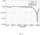
- FIG. 10 shows the RF performance of the base station antenna with the plurality of antenna elements of FIG. 9 dependent on the frequency.
- FIG. 10 shows the low frequency antenna (LFA) input matching as a function of the frequency.
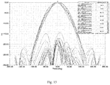
- FIG. 11 shows an LFA horizontal radiation pattern for the base station antenna according to FIG. 9 .
- FIG. 12 shows a high frequency antenna (HFA) input matching as a function of frequency for the same arrangement as in FIG. 10 and 11 .
- FIG. 13 shows a HFA horizontal radiation pattern for the same arrangement, namely the base station antenna of FIG. 9 .
- the present embodiments just show examples and are not limiting.
- the number of transmission lines of the first and second feeding circuit 130, 140 is not limited and can be arbitrary as long as the first and second feeding circuit 130, 140 serve for feeding the first and second radiating elements 150, 160 correspondingly.
- the first radiating element 150 is just exemplary formed by dipoles, but can be any first radiating element configured to radiate in any first operating frequency band.
- the radiating elements 150, 160 are dual polarized radiating elements in a further embodiment, the radiating elements could also be single polarized or even have more than two polarizations.
- the second radiating element 160 in the present embodiments is in a first alternative a bended metal sheet or in a second alternative a radiating element metallization and can be even formed as one part together with the support structure.
- the second radiating element can be shaped arbitrarily as long as the second radiating element is configured to radiate in a second operating frequency band being lower than the first operating frequency band of the first radiating element.
- the shape of the support structure of the discussed embodiments is just exemplary and can be any shape as long as the support structure is a single molded part. Further, the cavities and/or the hollows are optional. Further, the number of cavities can be arbitrarily chosen.
- the number of pins for the first and second feeding circuits and grounding pins and even the usage of pins instead of other connecting means is only exemplary and not limiting as long as the pins serve for its intended purposes.
- the provision of the first feeding circuit 130 on a surface of the first wall 126 facing the hollow area 128 is just exemplary and the first feeding circuit 130 in principle could also be arranged on any other surface of the support structure 120 or even within the support structure 120.
- the arrangement of the second feeding circuit 140 is just exemplary and could be provided on any surface of the support structure 120 or even within the support structure 120 as long as the feeding circuits fulfill their functions, namely that the first feeding circuit 130 is configured to feed the first radiating element 150 and the second feeding circuit 140 is configured to feed the second radiating element 160.
- the cutouts 161 in the second radiating element 160 and/or non-conductive interruptions 127 in the intermediate portion 121 are not essential and could also be omitted.
- the number of the cutouts 161 and/or the number of the non-conductive interruptions 127 is arbitrary.
- the example of the foot 115 being a printed circuit board is just an example not limiting the present invention and the foot 115 can be any element serving the intended purpose.
- the foot 115 in the embodiments of the present invention is just an optional feature.
- the number of ports and feeding lines within the foot 115 is arbitrary as long as the ports and/or feeding lines in the foot 115 fulfill its intended purpose.
Landscapes
- Physics & Mathematics (AREA)
- Electromagnetism (AREA)
- Engineering & Computer Science (AREA)
- Computer Networks & Wireless Communication (AREA)
- Variable-Direction Aerials And Aerial Arrays (AREA)
- Waveguide Aerials (AREA)
Description
- The present invention is directed to a dual-band antenna element and a base station comprising a plurality of said dual-band antenna elements.
- Today's base station antennas are operating in multiple bands typically with ± 45°polarization. Low-profile implementation of dual-band radiating elements plays a vital role for mass production. Printed circuit board technology was traditionally used to manufacture single or multiband elements. However, multiband antennas have more parts and hence multiple soldering joints. Such base station antennas are known e.g. from
EP 2 950 385 A1 ,WO 2012/055883 A1 orWO 2016/062356 . - Therefore, a problem of the present invention is to provide an improved concept for an antenna element.
- This problem is solved by the subject matter of a dual band antenna element of
claim 1 and a base station of claim 16. - Advantageous implementations of the present invention are further defined in the dependent claims 2-15.
- In a first aspect, a dual-band antenna element preferably for a base station antenna is provided, wherein the dual-band antenna element comprises: a support structure being a single molded part; a first feeding circuit and a second feeding circuit both arranged on the support structure; a first radiating element configured to radiate in a first operating frequency band and arranged on the support structure; wherein the first radiating element is fed by the first feeding circuit; a second radiating element configured to radiate in a second operating frequency band being lower than the first operating frequency band and arranged on the support structure; and wherein the second radiating element is fed by the second feeding circuit.
- In this context, the single molded part is a structure, which is a result of a molding process, for example, an injection molding process. Further, the first feeding circuit and the second feeding circuit can each be microstrip transmission lines. Accordingly, a dual-band antenna element is provided, which provides a high mechanical stability due to the provision of the single molded part. Further, due to the provision of the support structure as a single molded part a very simple and cost-effective manufacturing process of the dual-band antenna element is possible. Furthermore, the dual-band antenna element is very compact with only a few elements making up the dual-band antenna element, namely just the support structure, the first and second radiating element, which also reduces the number of any hand-soldered joints for connecting the elements of the dual band antenna element.
- Hence, an improved dual-band antenna element is provided which is simple to manufacture, provides a minimum number of parts and hand-soldered joints and at the same time provides good mechanical stability.
- In a first implementation form of the dual-band antenna element according to the first aspect, the support structure and the second radiating element are formed by a single molded partly metalized part; wherein the second radiating element is formed by a radiating element metallization on the single molded partly metalized part.
- Thereby, a very compact arrangement can be provided, in which the second radiating element is just formed by a metallization on the support structure, thereby further reducing the dimensions of the dual-band antenna element.
- In a second implementation form of the dual-band antenna element according to the first aspect, the second radiating element is a bended metal sheet attached to the support structure.
- This is an alternative in comparison to the first implementation form mentioned above, which also contributes for arriving at a very mechanically stable dual-band antenna element, which is also very compact and easy to manufacture.
- In the dual-band antenna element according to the first aspect, the support structure comprises a top portion, a bottom portion and a first wall connecting the top portion and the bottom portion, wherein at least a portion of the first wall surrounds a hollow area; wherein the first radiating element is arranged at the top portion; further comprising a first metallization forming the first feeding circuit and a balun metallization forming a balun for the first radiating element; wherein the first metallization and the balun metallization are arranged on opposing sides of the first wall and extend from the bottom portion to the top portion.
- Thereby, a very compact support structure can be provided in which, in a very effective way, the feeding of the first radiating element and the grounding of the first radiating element at the same time can be implemented.
- In the dual-band antenna element according to the first aspect, the support structure comprises an intermediate portion and a second wall connecting the bottom portion and the intermediate portion, wherein the first wall and the second wall enclose at least one cavity; wherein the second radiating element is arranged at the intermediate portion; further comprising a second metallization forming the second feeding circuit; wherein the second metallization is arranged on the second wall and extend from the bottom portion to the intermediate portion.
- Also this serves for providing a very compact dual-band antenna element, which implements both, a first and a second radiating element and the corresponding feeding and grounding circuitry and is at the same time mechanically stable and easy to manufacture.
- In a third implementation form of the dual-band antenna element according to the first aspect, the balun metallization is arranged on the side of the first wall facing the enclosed cavity and further extends along the side of the second wall facing the enclosed cavity, thereby serving as a ground plane for both, the first feeding circuit and the second feeding circuit.
- Thereby, in a very effective way a grounding plane can be provided for both, the first and second feeding circuit, which also contributes for arriving at a very compact dual-band antenna element having at the same time mechanical stability.
- In a fourth implementation form of the dual-band antenna element according to the first aspect, the second radiating element is a cup shaped element, having a bottom portion, a top portion and wall portion connecting the bottom portion and top portion.
- Accordingly, this provides a very compact second radiating element, which can be attached to the support structure, thereby providing a very compact dual-band antenna element.
- In a fifth implementation form of the dual-band antenna element according to the first aspect, the support structure comprises a or the bottom portion, an intermediate portion and a or the top portion, wherein the support structure extends from its bottom portion, through its intermediate portion to its top portion; wherein the second radiating element is arranged with its bottom portion on the intermediate portion of the support structure; wherein the bottom portion of the cup shaped element has an opening through which the support structure extends from the intermediate portion of the support structure to the top portion of support structure.
- Accordingly, due to the opening in the cup-shaped element making up the second radiating element, it is possible to provide in a very compact way both, the first and second radiating elements at the same time on the support structure, thereby contributing to the above-mentioned advantages of the dual-band antenna element.
- In a sixth implementation form of the dual-band antenna element according to the first aspect, the first radiating element is arranged at the top portion of the support structure.
- This contributes for arriving at a very compact dual-band antenna element comprising the first radiating element and the second radiating element.
- In a seventh implementation form of the dual-band antenna element according to the first aspect, the first radiating element is connected to the balun metallization.
- Thereby, a grounding of the first radiating element can be provided in a very effective way, which also contributes for arriving at a very compact dual-band antenna element providing at the same time mechanical stability.
- In an eighth implementation form of the dual-band antenna element according to the first aspect, the first feeding circuit comprises an open ended microstrip transmission line configured to feed the first radiating element and the second feeding circuit comprises a further open ended microstrip transmission line configured to feed the second radiating element.
- Thereby, because of the use of open ended microstrip transmission lines no galvanic connection between the radiating elements and feeding circuits is needed, which provides more freedom for arranging the first radiating element, the first feeding circuit, the second radiating element and the second feeding circuit.
- In a ninth implementation form of the dual-band antenna element according to the first aspect, the dual-band antenna element further comprises a foot at a or the bottom portion of the support structure, the foot comprising at least a first input port and a second input port; wherein the first input port is connected to the first feeding circuit and the second input port is connected to the second feeding circuit; wherein the input ports are configured to be connected to a distribution network of a base station antenna.
- Thereby, it is possible to effectively couple the dual-band antenna element to the distribution network of a base station antenna and ensuring at the same time the feeding of the first and second radiating elements.
- Furthermore, in another possible implementation form of any of the preceding implementation forms of the first aspect or the first aspect as such, the radiating elements are dual polarized radiating elements. In such an implementation form each of the feeding circuits provides a feeding for each of the two different polarizations of the radiating element it is configured to feed.
- Furthermore, in such implementation form with dual polarized radiating elements, where there is above mentioned foot arranged at the bottom portion of the support structure each input port pair comprises a first input port terminal for the first polarization and a second input port terminal for the second polarization. These input port terminals are connected to the corresponding feeding lines of the feeding circuits for the respective polarization.
- In a tenth implementation form of the dual-band antenna element according to the first aspect, the foot is a separate PCB soldered to the support structure. This further contributes for arriving at a very compact dual-band antenna element.
- In an eleventh implementation form of the dual-band antenna element according to the first aspect, the support structure together with the foot form the single molded part.
- Accordingly, a very compact dual-band antenna element being at the same time very stable can be provided. Furthermore, since the support structure and the foot together form the single molded product, no soldering joints are needed for attaching the support structure to the foot.
- In a twelfth implementation form of the dual-band antenna element according to the first aspect, the support structure together with the first radiating element and/or the second radiating element form the single molded part.
- Accordingly, this is a further implementation form for providing a very compact and stable dual-band antenna element, which is also easy to manufacture and no soldering joints are needed for attaching the first radiating element and/or the second radiating element to the support structure.
- In a thirteenth implementation form of the dual-band antenna element according to the first aspect, the first feeding circuit and the second feeding circuit are both formed by microstrip transmission lines.
- This implementation form aims at focusing on that the first feeding circuit is a microstrip transmission line and the second feeding circuit is also a microstrip transmission line, which provides for a very easy and effective implementation form of providing feeding circuits for the corresponding first and second radiating elements.
- In a fourteenth implementation form of the dual-band antenna element according to the first aspect, the dual-band antenna element is a molded interconnect device (MID).
- This further contributes to the advantages mentioned above concerning the first aspect and its implementation forms.
- In a second aspect, a base station is provided comprising a plurality of dual-band antenna elements according to the first aspect or the implementation forms of the first aspect.
- The above-described aspects and implementation forms of the present invention will be explained in the following description of specific embodiments in relation to enclosed drawings in which
- FIG. 1
- shows an exploded view of a dual-band antenna element according to a first embodiment of the present invention;
- FIG. 2
- shows a bottom view of a support structure of the dual-band antenna element according to the first embodiment of the present invention;
- FIG. 3
- shows a cross-sectional view of the support structure of the dual-band antenna element according to the first embodiment of the present invention;
- FIG.
- 4shows a top view of the support structure of the dual-band antenna element according to the first embodiment of the present invention;
- FIG. 5
- shows a printed circuit board of the dual-band antenna element according to the first embodiment of the present invention;
- FIG. 6A
- shows the support structure and the printed circuit board of the dual-band antenna element according to the first embodiment of the present invention in a first assembling step;
- FIG. 6B
- shows the support structure, the printed circuit board and a second radiating element of the dual-band antenna element according to the first embodiment of the present invention in a second assembling step;
- FIG. 6C
- shows the support structure, the printed circuit board, a first and the second radiating elements of the dual-band antenna element according to the first embodiment of the present invention in a third assembling step;
- FIG.
- 7 shows two further views on the support structure and the second radiating element of the dual band radiating element according to the first embodiment of the present invention;
- FIG. 8
- shows a photograph of the dual-band antenna element according to the first embodiment of the present invention;
- FIG. 9
- shows a schematic view of a base station antenna with a plurality of dual-band antenna elements according to the first or second embodiment of the present invention;
- FIG. 10
- shows an LFA input matching as a function of frequency for the base station antenna of
FIG. 9 ; - FIG. 11
- shows an LFA horizontal radiation pattern for the base station antenna of
FIG. 9 . - FIG. 12
- shows a HFA input matching as a function of frequency for the base station antenna of
FIG. 9 . - FIG. 13
- shows a HFA horizontal radiation pattern for the base station antenna of
FIG. 9 . -
FIG. 1 is an exploded view of a dual-band antenna element 100 preferably for a base station antenna, wherein the dual-band antenna element 100 comprises asupport structure 120 being a single molded part, a first feeding circuit 130 (not visible inFig. 1 , but inFig. 2 ) and a second feeding circuit 140 (only partly visible inFig. 1 , better to see inFig. 2 ), both arranged on thesupport structure 120, a first dual polarized radiatingelement 150 configured to radiate in a first operating frequency band and arranged on thesupport structure 120, wherein thefirst radiating element 150 is fed by the first feeding circuit 130, a second dual polarized radiatingelement 160 configured to radiate in a second operating frequency band being lower than the first operating frequency band and arranged on the support structure 120.Thesecond radiating element 160 is fed by thesecond feeding circuit 140. - As shown in
FIG. 1 , thesupport structure 120 comprises a top portion 122, abottom portion 124 and afirst wall 126 connecting the top portion 122 and thebottom portion 124, wherein a portion of thefirst wall 126 surrounds a hollow area 128 (thehollow area 128 is not visible in the exploded view ofFIG. 1 , but can be seen inFig. 2 ). - Further, the
support structure 120 comprises anintermediate portion 121 and asecond wall 123 connecting thebottom portion 124 and theintermediate portion 121, wherein thefirst wall 126 and thesecond wall 123 enclosecavities 125, which can also be seen in the exploded view ofFIG. 1 . In the embodiment ofFIG. 1 fourcavities 125 are provided, wherein two of the fourcavities 125 can be seen in the exploded view ofFIG. 1 and the other twocavities 125 are not visible due to the dome-shaped extension of thefirst wall 126 towards the top portion 122. - The
second radiating element 160 is arranged at theintermediate portion 121 on a surface of theintermediate portion 121 facing away thebottom portion 124 of thesupport structure 120. Further theantenna element 100 comprises abalun metallization 132. Thebalun metallization 132 forms a balun for thefirst radiating element 150 and thesecond radiating element 160 and therefore for grounding thefirst radiating element 150 and thesecond radiating element 160. Thebalun metallization 132 extends from the top portion 122 down to thebottom portion 124 on a surface of thefirst wall 126 facing away from the hollow area 128 (which encloses the first wall 126) and therefore is also partly provided on the surface of thefirst wall 126 facing thecavities 125. Further, thebalun metallization 132 can further extend along a surface of thesecond wall 126 facing theenclosed cavities 125 and can further extend on the surface of theintermediate portion 121 facing away from thebottom portion 124, thereby serving as a grounding plane for both, the first feeding circuit 130 and thesecond feeding circuit 140. Therefore, thebalun metallization 132 extends on an opposed surface of thesupport structure 120 as the first feeding circuits 130 and thesecond feeding circuits 140. Theintermediate portion 121 extends away from thefirst wall 126 in a direction perpendicular to a main extension direction, being a direction of a largest extension, of thefirst wall 126, wherein theintermediate portion 121 is provided in the main extension direction between the top portion 122 and thebottom portion 124 of thesupport structure 120. In thebalun metallization 132 provided on the surface of theintermediate portion 121 facing away from thebottom portion 124non-conductive interruptions 127, in particular slots, can be provided. Within thesenon-conductive interruptions 127 thebalun metallization 132 is not present, i.e. interrupted. In the embodiment ofFIG. 1 fourslots 127 are provided, wherein two diagonally opposingslots 127 serve for providing one polarization of the radiation emitted by thesecond radiating element 160, so that the fourslots 127 serve for providing two orthogonal polarizations for the second operating frequency band of thesecond radiating element 160. - Further, the
second radiating element 160 can be a bended metal sheet attached to thesupport structure 120. The bended metal sheet is in the form of a cup-shaped element having abottom portion 162, atop portion 164 and awall portion 166 connecting thebottom portion 162 and thetop portion 164. Further, thebottom portion 162 is formed by a sheet-like plate as can be seen inFIG. 1 . Fourcutouts 161 can extend from the respective corners of the sheet-like plate towards the middle of thebottom portion 162. Furthermore, in an assembled state, thesecond radiating element 160 is with itsbottom portion 162 attached to the surface of theintermediate portion 121 facing the top portion 122 of thesupport structure 120 in that way that in the direction from thebottom portion 124 to the top portion 122 of thesupport structure 120, onecutout 161 at least partially overlaps with a correspondingnon-conductive interruption 127, for example a slot, and thebalun metallization 132 faces thesecond radiating element 160. Thereby, two diagonally opposednon-conductive interruptions 127 together with the two correspondingcutouts 161 partially overlapping with the twonon-conductive interruptions 127 serve for providing one polarization, so that by the fourcutouts 161 together with the fournon-conductive interruptions 127 and corresponding open ended microstrip transmission lines of thesecond feeding circuit 140 feeding for the two orthogonal polarizations of thesecond radiating element 160 is provided. - Further, the
second radiating element 160 can comprise in a center portion of thebottom portion 162 anopening 163 through which thesupport structure 120 extends from theintermediate portion 121 of thesupport structure 120 to the top portion 122 of thesupport structure 120. - Further, in the embodiment shown in
FIG. 1 , thesecond feeding circuit 140 is formed by a second metallization, wherein the second metallization is arranged on a surface of thesecond wall 123 facing away from therespective cavity 125 and further extends on a surface of theintermediate portion 121 facing thebottom portion 124, so that the second metallization extends from thebottom portion 124 to and on theintermediate portion 121. - In the embodiments of the present invention, the first feeding circuit 130 is formed by two
microstrip transmission lines second feeding circuit 140 is formed by fourmicrostrip transmission lines 140a-140d. One of the microstrip transmission lines of thesecond feeding circuit 140 can also be seen inFIG. 1 on the surface of thesecond wall 123 facing away fromcavity 125, and this microstrip transmission line extends from thebottom portion 124 up to and on the surface of theintermediate portion 121 facing thebottom portion 124. Therefore, in the embodiment ofFIG. 1 fourmicrostrip transmission lines second feeding circuit 140 are provided, wherein in the exploded view ofFIG. 1 just one microstrip transmission line is visible. The fourmicrostrip transmission lines 140a-140d (best seen atFig. 2 ) of thesecond feeding circuit 140 also extend along a surface of theintermediate portion 121. Each polarization of thesecond radiating element 160 is fed by two opposing open ended microstrip transmission lines (140a, 140c and 140b, 140d) of thesecond feeding circuit 140. In other words the open ended microstrip transmission lines of thesecond feeding circuit 140, are provided pairwise diagonally opposite to each other on thesupport structure 120. Each pair of open ended microstrip transmission lines provided diagonally opposite to each other serves for generating a polarization of the radiation generated by thesecond radiating element 160, so that the four open endedmicrostrip transmission lines 140a-140d of thefeeding circuit 140 serve for providing two orthogonal polarizations of the radiation emitted by thesecond radiating element 160. - Furthermore, a first metallization forming the first feeding circuit 130 is provided. The first feeding circuit 130 can at best be seen in
Fig. 2 . The first feeding circuit 130 can be also by microstrip transmission lines, so that in the embodiment ofFIG.1 two open endedmicrostrip transmission lines microstrip transmission lines first wall 126 facing thehollow area 128 and extend from thebottom portion 124 to the top portion 122. Therefore, in the exploded view ofFIG. 1 , the twomicrostrip transmission lines - Furthermore, the
first radiating element 150 is provided on the top portion 122. In the embodiment ofFIG. 1 , the first dual polarized radiatingelement 150 is formed by two singlepolarized radiating elements polarized radiating elements support structure 151, being for example a PCB arranged at the top portion 122. Each dipole arm is formed by a metallization on a top surface of thesupport structure 151. Each singlepolarized radiating element polarized radiating element 150a is configured to radiate in a certain polarization being orthogonal to the polarization of the second singlepolarized radiating element 150b. The firstmicrostrip transmission line 130a of the first feeding circuit 130 extending from thebottom portion 124 to the top portion 122 is configured to feed the first singlepolarized radiating element 150a. The secondmicrostrip transmission line 130b of the first feeding circuit 130 extending from thebottom portion 124 to the top portion 122 is configured to feed the second singlepolarized radiating element 150b. - Furthermore, optionally, as can be seen in
FIG. 1 , afoot 115 can be provided at thebottom portion 124 of thesupport structure 120. Thefoot 115 comprises afirst input port 116 and asecond input port 117. Thefirst input port 116 is connected to the first feeding circuit 130 and thesecond input port 117 is connected to thesecond feeding circuit 140 and at the same time thefirst input port 116 and thesecond input port 117 are both configured to be connected to a distribution network of a base station antenna. - In detail, the
first input port 116 comprises a firstinput port terminal 116a and a secondinput port terminal 116b. The firstinput port terminal 116a of thefirst input port 116 is connected to the firstmicrostrip transmission line 130a for providing a feeding for the first polarization of the dual polarizedfirst radiating element 150. The secondinput port terminal 116b of thefirst input port 116 is connected to the secondmicrostrip transmission line 130b for providing a feeding for the second polarization of the dual polarizedfirst radiating element 150. - Furthermore, the
second input port 117 comprises a firstinput port terminal 117a and a secondinput port terminal 117b. The firstinput port terminal 117a of thesecond input port 117 is connected to the firstmicrostrip transmission line 140a and the thirdmicrostrip transmission line 140c of thefirst feeding circuit 140 for providing a feeding for the first polarization of the dual polarizedsecond radiating element 160. The secondinput port terminal 117b of thesecond input port 117 is connected to the secondmicrostrip transmission line 140b and the fourthmicrostrip transmission line 140d of thefirst feeding circuit 140 for providing a feeding for the second polarization of the dual polarizedsecond radiating element 160. - Further, the
bottom portion 124 of thesupport structure 120 can comprise pins (as further discussed with respect toFIG. 3 ) serving for connecting the first andsecond feeding circuits 130 and 140 to thefoot 115 and can furthermore comprise grounding pins (as further discussed with respect toFIG. 3 ) serving for connecting thebalun metallization 132 to thefoot 115, thereby providing a grounding. In the embodiment ofFIG. 1 , thefoot 115 is a separate PCB soldered to thesupport structure 120. Optionally, thefoot 115 together with thesupport structure 120 can form the single molded part instead of forming the single molded part only by thesupport structure 120. Further optionally, the single molded part can be formed by thesupport structure 120 together with thefoot 115 and thefirst radiating element 150 andsecond radiating element 160. Further, the dual band radiating element can be a molded interconnect device, MID. - The advantages achieved by the use of the molded interconnect device, MID, technology, are less number of parts, lightweight and it is suitable for mass production of antennas.
- The use of the MID technology allows the integration of feeding network, radiating elements and the support structure using a minimum amount of parts. Furthermore, the resulting dual band antenna element is operational in dual bands without sacrificing RF performance.
- To summarize, the dual band antenna element according to the first embodiment provides for a high mechanical stability due to the provision of the support structure being a single molded part on which the
first radiating element 150 and thesecond radiating element 160 are arranged. In addition, due to the provision of thesupport structure 120 as a single molded part a very simple and cost-effective manufacturing process of the dual-band antenna element 100 is possible. Furthermore, the dual-band antenna element 100 is very compact with only a few elements making up the dual-band antenna element 100, which also reduces the number of any hand-soldered joints for connecting the elements of the dualband antenna element 100. Further, since the first feeding circuit 130 andsecond feeding circuit 140 are provided on surfaces opposite to the surfaces on which thebalun metallization 132 is provided, a cross-over junction between the feeding circuits and thebalun metallization 132 can be avoided. -
FIG. 2 is a bottom view of thesupport structure 120 of the dual-band antenna element 100 according to the first embodiment. There, in the bottom view, thehollow area 128 is visible. Further, the twomicrostrip transmission lines microstrip transmission lines bottom portion 124 of thesupport structure 120 to the top portion 122. In particular, eachmicrostrip transmission line intersection area 180 of thebottom portion 124 between thefirst wall 126 and thesecond wall 123 to the top portion 122 on the surface of thefirst wall 126 facing thehollow area 128. Theintersection area 180 is shown inFIG. 2 as a surface area enclosing thehollow area 128 and on whichpins pins 141a -141d for thesecond feeding circuit 140 and groundingpins 190 for thebalun metallization 132 are provided. At the top portion 122, firstmicrostrip transmission line 130a has to bypass the secondmicrostrip transmission line 130b for not contacting the firstmicrostrip transmission line 130a, thereby avoiding a short circuit or interference between the signals fed by the twomicrostrip transmission lines microstrip transmission line 130b is provided outside thehollow area 128 for not contacting the firstmicrostrip transmission line 130a being provided on a surface of the top portion 122 facing thehollow area 128. Further, each of themicrostrip transmission lines polarized radiating element element 150. Hence, eachmicrostrip transmission line intersection area 180,pins microstrip transmission line FIG. 1 or2 a printed circuit board, as already mentioned with respect toFIG. 1 ). Thereby, the feeding offirst radiating element 150 is ensured. - Furthermore, the four
microstrip transmission lines 140a-140d of thesecond feeding circuit 140 extend from thebottom portion 124 on a surface of thesecond wall 123 facing away from thecorresponding cavity 125 and further extend on the surface of theintermediate portion 121 facing thebottom portion 124. In this context, fourcavities 125 are provided, which are not visible in the bottom view ofFIG. 2 , but are only visible in a top view. Two diagonally opposite arrangedmicrostrip transmission lines microstrip transmission lines microstrip transmission lines 140a-140d the two orthogonal polarizations of thesecond radiating element 160 are provided. - Further, pins 141a-141d for the
microstrip transmission lines 140a-140d are provided on theintersecting area 180, and eachpin 141a-141d galvanically contacts a correspondingmicrostrip transmission line 140a-140d of thesecond feeding circuit 140, thereby ensuring the feeding of thesecond radiating element 160. Further, eachpin 131a-b for the first feeding circuit 130 and eachpin 141a-d for thesecond feeding circuit 140 is configured to be connected to thefoot 115. Therefore, in this embodiment foursecond pins 141a-d for thesecond feeding circuit 140 are provided. All other pins shown on theintersecting area 180 are groundingpins 190 serving for ensuring a galvanic connection between thebalun metallization 132 and thefoot 115, thereby ensuring a grounding of thefirst radiating element 150 and thesecond radiating element 160. Of course in further embodiments some of the pins may be left floating and only serve for providing a mechanical connection between thesupport structure 120 and thefoot 115. -
FIG. 3 shows a cross-sectional view of thesupport structure 120 according to the first embodiment. There, thehollow area 128 is visible, which is surrounded by thefirst wall 126, wherein thefirst wall 126 extends from thebottom portion 124 to the top portion 122. Further, each of thecavities 125 is surrounded by a part of the surface of thefirst wall 126 facing thecavity 125 and a surface of thesecond wall 123 facing thecavity 125. Furthermore, a firstmicrostrip transmission line 130a is shown extending from apin 131a to the top portion 122. Furthermore, within the top portion 122 further grounding pins 190' are provided, which are galvanically connected to the corresponding first radiatingelement 150 and at the same time galvanically connected to the surface of thefirst wall 126 facing away thehollow area 128 on which thebalun metallization 132 is provided for ensuring a grounding of thefirst radiating element 150. Therefore, the grounding pins 190' on the top portion 122 extend through thefurther support structure 151 on which the metallization of the dipole arms of the singlepolarized radiating elements first radiating element 150 can be ensured, but this also contributes for maintaining a mechanical strength, so that the first radiating element 150 (or in more detail the further support structure 151) is tightly fixed to thesupport structure 120. Further, an additional air gap can be achieved between thesupport structure 120 and thefurther support structure 151 by the provision of conductive pads arranged on the grounding pins 190' at the top portion of thesupport structure 120. - Further, in
FIG. 3 onepin 141d for thesecond feeding circuit 140 is exemplary indicated. Thispin 141d is galvanically connected to the corresponding fourthmicrostrip transmission line 140d of thesecond feeding circuit 140. Furthermore, grounding pins 190 are provided in the bottom portion, wherein the grounding pins 190 in the bottom portion extend from thecorresponding cavity 125 through the material of thesupport structure 120 beyond theintersecting area 180, so that thebalun metallization 132 is electrically connected to the grounding pins 190, thereby ensuring a grounding of thefirst radiating element 150 and thesecond radiating element 160. Further, thepins 131a-131b for the first feeding circuit 130, thepins 141a-141d for thesecond feeding circuit 140 and the grounding pins 190 in thebottom portion 124 are configured to be connected to thefoot 115. - Therefore, the
microstrip transmission lines first wall 126 facing thehollow area 128 and themicrostrip transmission lines 140a-140d of thesecond feeding circuit 140 are provided on a surface of thesecond wall 123 facing away from thecorresponding cavity 125 and on the surface of theintermediate portion 121 facing thebottom portion 124. - Further, it should be noted that the cross-sectional view of
FIG. 3 shows the first embodiment with the material of thesupport structure 120 being transparent. - This is the reason why in this cross-sectional view of
FIG. 3 the fourthmicrostrip transmission line 140d of thesecond feeding circuit 140 is visible besides the firstmicrostrip transmission line 130a of the first feeding circuit 130. -
FIG. 4 shows a top view on thesupport structure 120 of the first embodiment, wherein again the material of thesupport structure 120 is made transparent. Therefore, in the top view, the twomicrostrip transmission lines microstrip transmission lines first wall 126 facing thehollow area 128. The twomicrostrip transmission lines microstrip transmission lines 140a-140d of thesecond feeding circuit 140 partly surrounds a correspondingnon-conductive interruption 127 and at the same time a portion of eachmicrostrip transmission line 140a-140d overlaps with a correspondingnon-conductive interruption 127. -
FIG. 5 shows thefoot 115 of the first embodiment of the dual-band antenna element 100. In particular, thefoot 115 in that embodiment is a printed circuit board. The printedcircuit board 115 comprises afirst input port 116 and asecond input port 117. Thefirst input port 116 comprises a firstinput port terminal 116a and a secondinput port terminal 116b. Thesecond input port 117 comprises a firstinput port terminal 117a and a secondinput port terminal 117b. With respect to thefirst input port 116, feedinglines 116a' and 116b' correspondingly extend from the corresponding firstinput port terminals PCB 115, which serve for connectingpins 131a-b for the first feeding circuit 130 of thesupport structure 120 tofoot 115. Thereby, a feeding of the first feeding circuit 130 of thesupport structure 120 is ensured. Further, each of the twoinput port terminals second input port 117 is connected to acorresponding feeding line 117a',117b', wherein each of thefeeding lines 117a',117b' branches into two sub-feeding lines and each of the sub-feeding lines further extends to corresponding ports within thePCB 115, which serve for connectingpins 141a-141b for thesecond feeding circuit 140 of thesupport structure 120 to thePCB 115, thereby ensuring a feeding of thesecond radiating element 160. In this context, thefirst feeding line 116a' serves for providing a first polarization for thefirst radiating element 150 and thesecond feeding line 116b' serves for providing a second polarization being orthogonal to the first polarization for thefirst radiating element 150. Further, thefirst feeding line 117a' serves for providing a first polarization for thesecond radiating element 160 and thesecond feeding line 117b' serves for providing a second polarization being orthogonal to the first polarization for thesecond radiating element 160. Each sub-feeding line of thefeeding lines 117a', 117b' is galvanically connected to onemicrostrip transmission line 140a-140d of thesecond feeding circuit 140. - Further, the grounding pins 190 provided in the
bottom portion 124 of thesupport structure 120 are connected to a metal (ground) layer on the bottom side of thePCB 115 and thepins 131a-b for the first feeding circuit 130 and thepins 141a-141d for thesecond feeding circuits 140 are connected to a metal (signal) layer on the top side of thePCB 115. - Furthermore,
FIGs. 6A-6C show schematically the steps for assembling the dual-band antenna element 100 of the first embodiment. Firstly, as shown inFIG. 6A , thesupport structure 120 is provided on thePCB 115 in that way that thePCB 115 is soldered together with thebottom portion 124 of thesupport structure 120. For doing this, thepins pins 141a-141d for thesecond feeding circuit 140 have to be provided within corresponding ports (metalized holes) provided withinPCB 115 and the grounding pins 190 in thebottom portion 124 of thesupport structure 120 are provided in corresponding ports of thePCB 115. Thesupport structure 120 is fixed to thePCB 115, e.g. by an automatic soldering process. In a next step, as shown inFIG. 6B , thesecond radiating element 160 is provided on theintermediate portion 121 of thesupport structure 120 in that way that acorresponding cutout 161 of thesecond radiating element 160 partially overlaps with a correspondingnon-conductive interruption 127 of thesupport structure 120. Thesecond radiating element 160 can be fixed to thesupport structure 120 by using e.g. plastic rivets. In a final step as shown inFIG. 6C , thefirst radiating element 150 is connected to thesupport structure 120 so that the grounding pins 190' on the top portion 122 extend through thefurther support structure 151 on which thefirst radiating element 150 is provided, thereby galvanically contacting the corresponding first radiatingelement 150. -
FIG. 7 shows two further views on the dualband radiating element 100 according to the first embodiment without thefirst radiating element 150 being arranged on thesupport structure 120. - Further, in a second embodiment being an alternative to the first embodiment, instead of providing the
second radiating element 160 being a bended metal sheet and thesupport structure 120 being the single molded part, it is conceivable that the support structure together with thesecond radiating element 160 are formed by a single molded partly metallized part. In such case, thesecond radiating element 160 is formed by a radiating element metallization on the single molded partly metallized part. Also, in this case the partly metallized part can be formed of partly metallized plastic. -
FIG. 8 shows a perspective view of the dual-band antenna element 100 according to the first embodiment in an assembled state. -
FIG. 9 shows a base station antenna with a plurality of dual-band antenna elements according to any of the embodiments of the present invention in an array configuration together with further radiating elements. -
FIG. 10 shows the RF performance of the base station antenna with the plurality of antenna elements ofFIG. 9 dependent on the frequency. In particular,FIG. 10 shows the low frequency antenna (LFA) input matching as a function of the frequency. Further,FIG. 11 shows an LFA horizontal radiation pattern for the base station antenna according toFIG. 9 . Further,FIG. 12 shows a high frequency antenna (HFA) input matching as a function of frequency for the same arrangement as inFIG. 10 and11 . Further,FIG. 13 shows a HFA horizontal radiation pattern for the same arrangement, namely the base station antenna ofFIG. 9 . - Furthermore, it should be noted that the present embodiments just show examples and are not limiting. For example, the number of transmission lines of the first and
second feeding circuit 130, 140 is not limited and can be arbitrary as long as the first andsecond feeding circuit 130, 140 serve for feeding the first and second radiatingelements first radiating element 150 is just exemplary formed by dipoles, but can be any first radiating element configured to radiate in any first operating frequency band. Furthermore, although the radiatingelements - Similarly, the
second radiating element 160 in the present embodiments is in a first alternative a bended metal sheet or in a second alternative a radiating element metallization and can be even formed as one part together with the support structure. However, this is just an example and the second radiating element can be shaped arbitrarily as long as the second radiating element is configured to radiate in a second operating frequency band being lower than the first operating frequency band of the first radiating element. Furthermore, the shape of the support structure of the discussed embodiments is just exemplary and can be any shape as long as the support structure is a single molded part. Further, the cavities and/or the hollows are optional. Further, the number of cavities can be arbitrarily chosen. Furthermore, the number of pins for the first and second feeding circuits and grounding pins and even the usage of pins instead of other connecting means is only exemplary and not limiting as long as the pins serve for its intended purposes. Furthermore, the provision of the first feeding circuit 130 on a surface of thefirst wall 126 facing thehollow area 128 is just exemplary and the first feeding circuit 130 in principle could also be arranged on any other surface of thesupport structure 120 or even within thesupport structure 120. Similarly, also the arrangement of thesecond feeding circuit 140 is just exemplary and could be provided on any surface of thesupport structure 120 or even within thesupport structure 120 as long as the feeding circuits fulfill their functions, namely that the first feeding circuit 130 is configured to feed thefirst radiating element 150 and thesecond feeding circuit 140 is configured to feed thesecond radiating element 160. Further, thecutouts 161 in thesecond radiating element 160 and/ornon-conductive interruptions 127 in theintermediate portion 121 are not essential and could also be omitted. Further, the number of thecutouts 161 and/or the number of thenon-conductive interruptions 127 is arbitrary. Furthermore, the example of thefoot 115 being a printed circuit board is just an example not limiting the present invention and thefoot 115 can be any element serving the intended purpose. Furthermore, thefoot 115 in the embodiments of the present invention is just an optional feature. Further, the number of ports and feeding lines within thefoot 115 is arbitrary as long as the ports and/or feeding lines in thefoot 115 fulfill its intended purpose. - The invention has been described in conjunction with two embodiments. However, other variations to the enclosed embodiments can be understood and effected by those skilled in the art and practitioning the claimed invention, from a study of the drawings, the disclosure and the appended claims. In these claims, the word "comprising" does not exclude other elements or steps and the indefinite article "a" or "an" does not exclude a plurality. The mere fact that certain measures are recited in mutually different dependent claims does not indicate that a combination of these measures cannot be used to advantage.
Claims (16)
- A dual band antenna element (100), the dual band antenna element (100) comprising:• a support structure (120) being a single molded part; a first feeding circuit (130) and a second feeding circuit (140) both arranged on the support structure (120);• a first radiating element (150) configured to radiate in a first operating frequency band and arranged on the support structure (120);• wherein the first radiating element (150) is fed by the first feeding circuit (130);• a second radiating element (160) configured to radiate in a second operating frequency band being lower than the first operating frequency band and arranged on the support structure (120); and• wherein the second radiating element is fed by the second feeding circuit (140),• wherein the support structure (120) comprises a top portion (122), a bottom portion (124) and a first wall (126) connecting the top portion (122) and the bottom portion (124), wherein at least a portion of the first wall (126) surrounds a hollow area (128);• wherein the first radiating element (150) is arranged at the top portion (122); further comprising a first metallization forming the first feeding circuit (130) and a balun metallization (132) forming a balun for the first radiating element (150); wherein the first metallization and the balun metallization (132) are arranged on opposing sides of the first wall (126) and extend from the bottom portion (124) to the top portion (122),• wherein the support structure (120) comprises an intermediate portion (121) and a second wall (123) connecting the bottom portion (124) and the intermediate portion (121), wherein the first wall (126) and the second wall (123) enclose at least one cavity (125);• wherein the second radiating element (160) is arranged at the intermediate portion (121); further comprising a second metallization forming the second feeding circuit (140);• wherein the second metallization is arranged on the second wall (123) and extend from the bottom portion (124) to the intermediate portion (121).
- The dual band antenna element (100) according to claim 1,wherein the support structure (120) and the second radiating element (160) are formed by a single molded partly metalized part;wherein the second radiating element (160) is formed by a radiating element metallization on the single molded partly metalized part.
- The dual band antenna element (100) according to claim 1, wherein the second radiating element (160) is a bended metal sheet attached to the support structure (120).
- The dual band antenna element (100) according to claim 1, wherein the balun metallization (132) is arranged on the side of the first wall (126) facing the at least one cavity (125) and further extends along the side of the second wall (123) facing the at least one cavity (125), thereby serving as a ground plane for both, the first feeding circuit (130) and the second feeding circuit (140).
- The dual band antenna element (100) according to any of the preceding claims,
wherein the second radiating element (160) is a cup shaped element, having a bottom portion (162), a top portion (164) and wall portion (166) connecting the bottom portion (162) and top portion (164). - The dual band antenna element (100) according to claim 5, wherein the support structure (120) comprises the bottom portion (124), the intermediate portion (121) and the top portion (122), wherein the support structure (120) extends from its bottom portion (124), through its intermediate portion (121) to its top portion (122);
wherein the second radiating element (160) is arranged with its bottom portion (162) on the intermediate portion (121) of the support structure (120);
wherein the bottom portion (162) of the cup shaped element has an opening (163) through which the support structure (120) extends from the intermediate portion (121) of the support structure (120) to the top portion (122) of support structure (120). - The dual band antenna element (100) according to claim 6, wherein the first radiating element (150) is arranged at the top portion (122) of the support structure (120).
- The dual-band antenna element (100) according to claim 7, wherein the first radiating element (150) is connected to the balun metallization (132).
- The dual-band antenna element (100) according to any of the preceding claims, wherein the first feeding circuit (130) comprises an open ended microstrip transmission line configured to feed the first radiating element (150) and the second feeding circuit (140) comprises a further open ended microstrip transmission line configured to feed the second radiating element (160).
- The dual band antenna element (100) according to any of the preceding claims, further comprising
a foot (115) at the bottom portion (124) of the support structure (120), the foot (115) comprising at least a first input port (116) and a second input port (117); wherein the first input port (116) is connected to the first feeding circuit (130) and the second input port (117) is connected to the second feeding circuit (140); wherein the input ports (116, 117) are configured to be connected to a distribution network of a base station antenna. - The dual band antenna element (100) according to claim 10, wherein the foot (115) is a separate PCB soldered to the support structure (120).
- The dual band antenna element (100) according to claim 10, wherein the support structure (120) together with the foot (115) form the single molded part.
- The dual band antenna element (100) according to any of the preceding claims, wherein the support structure (120) together with the first radiating element (150) and/or the second radiating element (160) form the single molded part.
- The dual band antenna element (100) according to any of the preceding claims, wherein said first feeding circuit (130) and said second feeding circuit (140) are both formed by microstrip transmission lines.
- The dual band antenna element (100) according to any of the preceding claims, wherein the dual band antenna element is at least partly a Molded Interconnect Device, MID.
- A base station comprising a plurality of dual band antenna elements (100) according to any of the preceding claims.
Applications Claiming Priority (1)
| Application Number | Priority Date | Filing Date | Title |
|---|---|---|---|
| PCT/EP2016/079826 WO2018103822A1 (en) | 2016-12-06 | 2016-12-06 | Dual-band antenna element and base station |
Publications (2)
| Publication Number | Publication Date |
|---|---|
| EP3535806A1 EP3535806A1 (en) | 2019-09-11 |
| EP3535806B1 true EP3535806B1 (en) | 2021-07-28 |
Family
ID=57482448
Family Applications (1)
| Application Number | Title | Priority Date | Filing Date |
|---|---|---|---|
| EP16805857.6A Active EP3535806B1 (en) | 2016-12-06 | 2016-12-06 | Dual-band antenna element and base station |
Country Status (4)
| Country | Link |
|---|---|
| US (1) | US10950926B2 (en) |
| EP (1) | EP3535806B1 (en) |
| CN (1) | CN110235306B (en) |
| WO (1) | WO2018103822A1 (en) |
Cited By (1)
| Publication number | Priority date | Publication date | Assignee | Title |
|---|---|---|---|---|
| US12300907B2 (en) | 2020-08-17 | 2025-05-13 | Huawei Technologies Co., Ltd. | Antenna element for a multi-band antenna device |
Families Citing this family (16)
| Publication number | Priority date | Publication date | Assignee | Title |
|---|---|---|---|---|
| KR101609665B1 (en) * | 2014-11-11 | 2016-04-06 | 주식회사 케이엠더블유 | Antenna of mobile communication station |
| EP3627622B1 (en) * | 2017-05-17 | 2022-08-24 | Tongyu Communication Inc. | Radiation element, as well as antenna unit and antenna array thereof |
| WO2018218603A1 (en) * | 2017-06-01 | 2018-12-06 | 华为技术有限公司 | Dual-polarized radiation unit, antenna, base station and communication system |
| CN111029727A (en) * | 2019-12-09 | 2020-04-17 | 瑞声科技(新加坡)有限公司 | Antenna unit and base station |
| KR102234510B1 (en) | 2019-12-10 | 2021-03-30 | 연세대학교 산학협력단 | Dual Band Antenna |
| WO2021150365A1 (en) * | 2020-01-21 | 2021-07-29 | John Mezzalingua Associates, LLC | Multi-band antenna array face and radiator configuration for mitigating interference |
| US11611143B2 (en) | 2020-03-24 | 2023-03-21 | Commscope Technologies Llc | Base station antenna with high performance active antenna system (AAS) integrated therein |
| EP4429025A3 (en) | 2020-03-24 | 2024-11-20 | Outdoor Wireless Networks LLC | Radiating elements having angled feed stalks and base station antennas including same |
| EP3966898A4 (en) | 2020-03-24 | 2023-01-25 | CommScope Technologies LLC | ACTIVE ANTENNA MODULE BASE STATION ANTENNAS AND RELATED DEVICES AND METHODS |
| US12218425B2 (en) | 2020-04-28 | 2025-02-04 | Outdoor Wireless Networks LLC | Base station antennas having reflector assemblies including a nonmetallic substrate having a metallic layer thereon |
| EP4139990A1 (en) * | 2020-05-14 | 2023-03-01 | Huawei Technologies Co., Ltd. | Antenna device, array of antenna devices, and base station |
| WO2022032664A1 (en) * | 2020-08-14 | 2022-02-17 | Telefonaktiebolaget Lm Ericsson (Publ) | Base station |
| CN116057779B (en) | 2020-09-14 | 2025-05-30 | 华为技术有限公司 | Antenna device, antenna device array and base station with antenna device |
| CN215418610U (en) | 2021-08-31 | 2022-01-04 | 康普技术有限责任公司 | Frequency selective reflector and base station antenna |
| CN117199772A (en) | 2022-06-01 | 2023-12-08 | 康普技术有限责任公司 | Base station antenna |
| US12469960B2 (en) | 2022-07-08 | 2025-11-11 | Outdoor Wireless Networks LLC | Base station antennas |
Family Cites Families (10)
| Publication number | Priority date | Publication date | Assignee | Title |
|---|---|---|---|---|
| DE10203873A1 (en) | 2002-01-31 | 2003-08-14 | Kathrein Werke Kg | Dual polarized radiator arrangement |
| US6747606B2 (en) * | 2002-05-31 | 2004-06-08 | Radio Frequency Systems Inc. | Single or dual polarized molded dipole antenna having integrated feed structure |
| FR2966986B1 (en) * | 2010-10-27 | 2013-07-12 | Alcatel Lucent | RADIANT ELEMENT OF ANTENNA |
| EP2727183B1 (en) | 2011-06-30 | 2016-11-16 | Gapwaves AB | Improved broadband multi-dipole antenna with frequency-independent radiation characteristics |
| CN202888396U (en) * | 2012-10-29 | 2013-04-17 | 江苏亨鑫科技有限公司 | Low-frequency dual-polarization folded antenna dipole |
| CN203071221U (en) * | 2012-12-18 | 2013-07-17 | 张家港保税区国信通信有限公司 | Wideband dual-polarization radiation unit |
| EP2950385B1 (en) * | 2014-05-28 | 2016-08-24 | Alcatel Lucent | Multiband antenna |
| WO2016062356A1 (en) * | 2014-10-24 | 2016-04-28 | Huawei Technologies Co.,Ltd. | Antenna device for a base station antenna system |
| EP3166178B1 (en) | 2015-11-03 | 2019-09-11 | Huawei Technologies Co., Ltd. | An antenna element preferably for a base station antenna |
| EP3813192B1 (en) | 2016-04-12 | 2022-09-28 | Huawei Technologies Co., Ltd. | Ultra broad band dual polarized radiating element for a base station antenna |
-
2016
- 2016-12-06 EP EP16805857.6A patent/EP3535806B1/en active Active
- 2016-12-06 WO PCT/EP2016/079826 patent/WO2018103822A1/en not_active Ceased
- 2016-12-06 CN CN201680091171.7A patent/CN110235306B/en active Active
-
2019
- 2019-06-05 US US16/432,462 patent/US10950926B2/en active Active
Cited By (1)
| Publication number | Priority date | Publication date | Assignee | Title |
|---|---|---|---|---|
| US12300907B2 (en) | 2020-08-17 | 2025-05-13 | Huawei Technologies Co., Ltd. | Antenna element for a multi-band antenna device |
Also Published As
| Publication number | Publication date |
|---|---|
| US20190312338A1 (en) | 2019-10-10 |
| US10950926B2 (en) | 2021-03-16 |
| WO2018103822A1 (en) | 2018-06-14 |
| CN110235306A (en) | 2019-09-13 |
| EP3535806A1 (en) | 2019-09-11 |
| CN110235306B (en) | 2020-12-25 |
Similar Documents
| Publication | Publication Date | Title |
|---|---|---|
| US10950926B2 (en) | Dual-band antenna element and base station | |
| JP7083401B2 (en) | Double-polarized antenna and dual-polarized antenna assembly including it | |
| CN109792109B (en) | Antenna element | |
| CA2915243C (en) | Switchable transmit and receive phased array antenna | |
| US10756445B2 (en) | Switchable transmit and receive phased array antenna with high power and compact size | |
| US10461420B2 (en) | Switchable transmit and receive phased array antenna | |
| EP3166178A1 (en) | An antenna element preferably for a base station antenna | |
| KR101778595B1 (en) | Vivaldi antenna apparatus | |
| US20040183728A1 (en) | Multi-Band Omni Directional Antenna | |
| CN111697320A (en) | Antenna device, antenna module, and communication device | |
| WO2014018600A1 (en) | Dual-polarized radiating element with enhanced isolation for use in antenna system | |
| JP7025843B2 (en) | Antenna and antenna module containing the antenna | |
| US20120182190A1 (en) | Portable wireless device | |
| JP7059385B2 (en) | Antenna module and communication device equipped with it | |
| JP2020156077A (en) | Antenna device, antenna module, and communication device | |
| US20240145893A1 (en) | Radio frequency filters covered by printed circuit boards | |
| US10868369B2 (en) | Antenna module | |
| CN220527199U (en) | Flat dual-frequency patch antenna | |
| EP3794680B1 (en) | Patch antenna design for easy fabrication and controllable performance at high frequency bands | |
| CN113875087A (en) | Antenna unit and communication apparatus | |
| IL294914A (en) | Slot antenna array | |
| US10879582B1 (en) | Dielectric reinforced formed metal antenna | |
| EP4135126B1 (en) | Uwb antenna | |
| US20220359986A1 (en) | Antenna system with short cable | |
| KR20220078202A (en) | Microstrip antenna and microstrip antenna module including coupling member |
Legal Events
| Date | Code | Title | Description |
|---|---|---|---|
| STAA | Information on the status of an ep patent application or granted ep patent |
Free format text: STATUS: UNKNOWN |
|
| STAA | Information on the status of an ep patent application or granted ep patent |
Free format text: STATUS: THE INTERNATIONAL PUBLICATION HAS BEEN MADE |
|
| PUAI | Public reference made under article 153(3) epc to a published international application that has entered the european phase |
Free format text: ORIGINAL CODE: 0009012 |
|
| STAA | Information on the status of an ep patent application or granted ep patent |
Free format text: STATUS: REQUEST FOR EXAMINATION WAS MADE |
|
| 17P | Request for examination filed |
Effective date: 20190605 |
|
| AK | Designated contracting states |
Kind code of ref document: A1 Designated state(s): AL AT BE BG CH CY CZ DE DK EE ES FI FR GB GR HR HU IE IS IT LI LT LU LV MC MK MT NL NO PL PT RO RS SE SI SK SM TR |
|
| AX | Request for extension of the european patent |
Extension state: BA ME |
|
| DAV | Request for validation of the european patent (deleted) | ||
| DAX | Request for extension of the european patent (deleted) | ||
| GRAP | Despatch of communication of intention to grant a patent |
Free format text: ORIGINAL CODE: EPIDOSNIGR1 |
|
| STAA | Information on the status of an ep patent application or granted ep patent |
Free format text: STATUS: GRANT OF PATENT IS INTENDED |
|
| INTG | Intention to grant announced |
Effective date: 20210309 |
|
| RIN1 | Information on inventor provided before grant (corrected) |
Inventor name: SEGADOR ALVAREZ, JUAN Inventor name: GUNTUPALLI, AJAY, BABU Inventor name: BISCONTINI, BRUNO Inventor name: REBEGEA, SERBAN Inventor name: RIST, BERNHARD |
|
| GRAS | Grant fee paid |
Free format text: ORIGINAL CODE: EPIDOSNIGR3 |
|
| GRAA | (expected) grant |
Free format text: ORIGINAL CODE: 0009210 |
|
| STAA | Information on the status of an ep patent application or granted ep patent |
Free format text: STATUS: THE PATENT HAS BEEN GRANTED |
|
| AK | Designated contracting states |
Kind code of ref document: B1 Designated state(s): AL AT BE BG CH CY CZ DE DK EE ES FI FR GB GR HR HU IE IS IT LI LT LU LV MC MK MT NL NO PL PT RO RS SE SI SK SM TR |
|
| REG | Reference to a national code |
Ref country code: GB Ref legal event code: FG4D |
|
| REG | Reference to a national code |
Ref country code: CH Ref legal event code: EP |
|
| REG | Reference to a national code |
Ref country code: DE Ref legal event code: R096 Ref document number: 602016061310 Country of ref document: DE |
|
| REG | Reference to a national code |
Ref country code: AT Ref legal event code: REF Ref document number: 1415540 Country of ref document: AT Kind code of ref document: T Effective date: 20210815 |
|
| REG | Reference to a national code |
Ref country code: IE Ref legal event code: FG4D |
|
| REG | Reference to a national code |
Ref country code: LT Ref legal event code: MG9D |
|
| REG | Reference to a national code |
Ref country code: NL Ref legal event code: MP Effective date: 20210728 |
|
| REG | Reference to a national code |
Ref country code: AT Ref legal event code: MK05 Ref document number: 1415540 Country of ref document: AT Kind code of ref document: T Effective date: 20210728 |
|
| PG25 | Lapsed in a contracting state [announced via postgrant information from national office to epo] |
Ref country code: RS Free format text: LAPSE BECAUSE OF FAILURE TO SUBMIT A TRANSLATION OF THE DESCRIPTION OR TO PAY THE FEE WITHIN THE PRESCRIBED TIME-LIMIT Effective date: 20210728 Ref country code: SE Free format text: LAPSE BECAUSE OF FAILURE TO SUBMIT A TRANSLATION OF THE DESCRIPTION OR TO PAY THE FEE WITHIN THE PRESCRIBED TIME-LIMIT Effective date: 20210728 Ref country code: LT Free format text: LAPSE BECAUSE OF FAILURE TO SUBMIT A TRANSLATION OF THE DESCRIPTION OR TO PAY THE FEE WITHIN THE PRESCRIBED TIME-LIMIT Effective date: 20210728 Ref country code: BG Free format text: LAPSE BECAUSE OF FAILURE TO SUBMIT A TRANSLATION OF THE DESCRIPTION OR TO PAY THE FEE WITHIN THE PRESCRIBED TIME-LIMIT Effective date: 20211028 Ref country code: AT Free format text: LAPSE BECAUSE OF FAILURE TO SUBMIT A TRANSLATION OF THE DESCRIPTION OR TO PAY THE FEE WITHIN THE PRESCRIBED TIME-LIMIT Effective date: 20210728 Ref country code: HR Free format text: LAPSE BECAUSE OF FAILURE TO SUBMIT A TRANSLATION OF THE DESCRIPTION OR TO PAY THE FEE WITHIN THE PRESCRIBED TIME-LIMIT Effective date: 20210728 Ref country code: FI Free format text: LAPSE BECAUSE OF FAILURE TO SUBMIT A TRANSLATION OF THE DESCRIPTION OR TO PAY THE FEE WITHIN THE PRESCRIBED TIME-LIMIT Effective date: 20210728 Ref country code: ES Free format text: LAPSE BECAUSE OF FAILURE TO SUBMIT A TRANSLATION OF THE DESCRIPTION OR TO PAY THE FEE WITHIN THE PRESCRIBED TIME-LIMIT Effective date: 20210728 Ref country code: PT Free format text: LAPSE BECAUSE OF FAILURE TO SUBMIT A TRANSLATION OF THE DESCRIPTION OR TO PAY THE FEE WITHIN THE PRESCRIBED TIME-LIMIT Effective date: 20211129 Ref country code: NO Free format text: LAPSE BECAUSE OF FAILURE TO SUBMIT A TRANSLATION OF THE DESCRIPTION OR TO PAY THE FEE WITHIN THE PRESCRIBED TIME-LIMIT Effective date: 20211028 Ref country code: NL Free format text: LAPSE BECAUSE OF FAILURE TO SUBMIT A TRANSLATION OF THE DESCRIPTION OR TO PAY THE FEE WITHIN THE PRESCRIBED TIME-LIMIT Effective date: 20210728 |
|
| PG25 | Lapsed in a contracting state [announced via postgrant information from national office to epo] |
Ref country code: PL Free format text: LAPSE BECAUSE OF FAILURE TO SUBMIT A TRANSLATION OF THE DESCRIPTION OR TO PAY THE FEE WITHIN THE PRESCRIBED TIME-LIMIT Effective date: 20210728 Ref country code: LV Free format text: LAPSE BECAUSE OF FAILURE TO SUBMIT A TRANSLATION OF THE DESCRIPTION OR TO PAY THE FEE WITHIN THE PRESCRIBED TIME-LIMIT Effective date: 20210728 Ref country code: GR Free format text: LAPSE BECAUSE OF FAILURE TO SUBMIT A TRANSLATION OF THE DESCRIPTION OR TO PAY THE FEE WITHIN THE PRESCRIBED TIME-LIMIT Effective date: 20211029 |
|
| PG25 | Lapsed in a contracting state [announced via postgrant information from national office to epo] |
Ref country code: DK Free format text: LAPSE BECAUSE OF FAILURE TO SUBMIT A TRANSLATION OF THE DESCRIPTION OR TO PAY THE FEE WITHIN THE PRESCRIBED TIME-LIMIT Effective date: 20210728 |
|
| REG | Reference to a national code |
Ref country code: DE Ref legal event code: R097 Ref document number: 602016061310 Country of ref document: DE |
|
| PG25 | Lapsed in a contracting state [announced via postgrant information from national office to epo] |
Ref country code: SM Free format text: LAPSE BECAUSE OF FAILURE TO SUBMIT A TRANSLATION OF THE DESCRIPTION OR TO PAY THE FEE WITHIN THE PRESCRIBED TIME-LIMIT Effective date: 20210728 Ref country code: SK Free format text: LAPSE BECAUSE OF FAILURE TO SUBMIT A TRANSLATION OF THE DESCRIPTION OR TO PAY THE FEE WITHIN THE PRESCRIBED TIME-LIMIT Effective date: 20210728 Ref country code: RO Free format text: LAPSE BECAUSE OF FAILURE TO SUBMIT A TRANSLATION OF THE DESCRIPTION OR TO PAY THE FEE WITHIN THE PRESCRIBED TIME-LIMIT Effective date: 20210728 Ref country code: EE Free format text: LAPSE BECAUSE OF FAILURE TO SUBMIT A TRANSLATION OF THE DESCRIPTION OR TO PAY THE FEE WITHIN THE PRESCRIBED TIME-LIMIT Effective date: 20210728 Ref country code: CZ Free format text: LAPSE BECAUSE OF FAILURE TO SUBMIT A TRANSLATION OF THE DESCRIPTION OR TO PAY THE FEE WITHIN THE PRESCRIBED TIME-LIMIT Effective date: 20210728 Ref country code: AL Free format text: LAPSE BECAUSE OF FAILURE TO SUBMIT A TRANSLATION OF THE DESCRIPTION OR TO PAY THE FEE WITHIN THE PRESCRIBED TIME-LIMIT Effective date: 20210728 |
|
| PLBE | No opposition filed within time limit |
Free format text: ORIGINAL CODE: 0009261 |
|
| STAA | Information on the status of an ep patent application or granted ep patent |
Free format text: STATUS: NO OPPOSITION FILED WITHIN TIME LIMIT |
|
| 26N | No opposition filed |
Effective date: 20220429 |
|
| PG25 | Lapsed in a contracting state [announced via postgrant information from national office to epo] |
Ref country code: MC Free format text: LAPSE BECAUSE OF FAILURE TO SUBMIT A TRANSLATION OF THE DESCRIPTION OR TO PAY THE FEE WITHIN THE PRESCRIBED TIME-LIMIT Effective date: 20210728 Ref country code: IT Free format text: LAPSE BECAUSE OF FAILURE TO SUBMIT A TRANSLATION OF THE DESCRIPTION OR TO PAY THE FEE WITHIN THE PRESCRIBED TIME-LIMIT Effective date: 20210728 |
|
| REG | Reference to a national code |
Ref country code: CH Ref legal event code: PL |
|
| REG | Reference to a national code |
Ref country code: BE Ref legal event code: MM Effective date: 20211231 |
|
| PG25 | Lapsed in a contracting state [announced via postgrant information from national office to epo] |
Ref country code: LU Free format text: LAPSE BECAUSE OF NON-PAYMENT OF DUE FEES Effective date: 20211206 Ref country code: IE Free format text: LAPSE BECAUSE OF NON-PAYMENT OF DUE FEES Effective date: 20211206 |
|
| PG25 | Lapsed in a contracting state [announced via postgrant information from national office to epo] |
Ref country code: FR Free format text: LAPSE BECAUSE OF NON-PAYMENT OF DUE FEES Effective date: 20211231 Ref country code: BE Free format text: LAPSE BECAUSE OF NON-PAYMENT OF DUE FEES Effective date: 20211231 |
|
| PG25 | Lapsed in a contracting state [announced via postgrant information from national office to epo] |
Ref country code: LI Free format text: LAPSE BECAUSE OF NON-PAYMENT OF DUE FEES Effective date: 20211231 Ref country code: CH Free format text: LAPSE BECAUSE OF NON-PAYMENT OF DUE FEES Effective date: 20211231 |
|
| PG25 | Lapsed in a contracting state [announced via postgrant information from national office to epo] |
Ref country code: CY Free format text: LAPSE BECAUSE OF FAILURE TO SUBMIT A TRANSLATION OF THE DESCRIPTION OR TO PAY THE FEE WITHIN THE PRESCRIBED TIME-LIMIT Effective date: 20210728 |
|
| PG25 | Lapsed in a contracting state [announced via postgrant information from national office to epo] |
Ref country code: HU Free format text: LAPSE BECAUSE OF FAILURE TO SUBMIT A TRANSLATION OF THE DESCRIPTION OR TO PAY THE FEE WITHIN THE PRESCRIBED TIME-LIMIT; INVALID AB INITIO Effective date: 20161206 |
|
| PG25 | Lapsed in a contracting state [announced via postgrant information from national office to epo] |
Ref country code: MK Free format text: LAPSE BECAUSE OF FAILURE TO SUBMIT A TRANSLATION OF THE DESCRIPTION OR TO PAY THE FEE WITHIN THE PRESCRIBED TIME-LIMIT Effective date: 20210728 |
|
| PG25 | Lapsed in a contracting state [announced via postgrant information from national office to epo] |
Ref country code: MT Free format text: LAPSE BECAUSE OF FAILURE TO SUBMIT A TRANSLATION OF THE DESCRIPTION OR TO PAY THE FEE WITHIN THE PRESCRIBED TIME-LIMIT Effective date: 20210728 |
|
| PG25 | Lapsed in a contracting state [announced via postgrant information from national office to epo] |
Ref country code: TR Free format text: LAPSE BECAUSE OF FAILURE TO SUBMIT A TRANSLATION OF THE DESCRIPTION OR TO PAY THE FEE WITHIN THE PRESCRIBED TIME-LIMIT Effective date: 20210728 |
|
| PGFP | Annual fee paid to national office [announced via postgrant information from national office to epo] |
Ref country code: DE Payment date: 20251104 Year of fee payment: 10 |
|
| PGFP | Annual fee paid to national office [announced via postgrant information from national office to epo] |
Ref country code: GB Payment date: 20251030 Year of fee payment: 10 |