EP3534519A1 - Power conversion device - Google Patents
Power conversion device Download PDFInfo
- Publication number
- EP3534519A1 EP3534519A1 EP16919803.3A EP16919803A EP3534519A1 EP 3534519 A1 EP3534519 A1 EP 3534519A1 EP 16919803 A EP16919803 A EP 16919803A EP 3534519 A1 EP3534519 A1 EP 3534519A1
- Authority
- EP
- European Patent Office
- Prior art keywords
- negative terminal
- capacitor
- isolation transformer
- conversion device
- power conversion
- Prior art date
- Legal status (The legal status is an assumption and is not a legal conclusion. Google has not performed a legal analysis and makes no representation as to the accuracy of the status listed.)
- Granted
Links
Images






Classifications
-
- H—ELECTRICITY
- H02—GENERATION; CONVERSION OR DISTRIBUTION OF ELECTRIC POWER
- H02M—APPARATUS FOR CONVERSION BETWEEN AC AND AC, BETWEEN AC AND DC, OR BETWEEN DC AND DC, AND FOR USE WITH MAINS OR SIMILAR POWER SUPPLY SYSTEMS; CONVERSION OF DC OR AC INPUT POWER INTO SURGE OUTPUT POWER; CONTROL OR REGULATION THEREOF
- H02M7/00—Conversion of AC power input into DC power output; Conversion of DC power input into AC power output
- H02M7/02—Conversion of AC power input into DC power output without possibility of reversal
- H02M7/04—Conversion of AC power input into DC power output without possibility of reversal by static converters
- H02M7/06—Conversion of AC power input into DC power output without possibility of reversal by static converters using discharge tubes without control electrode or semiconductor devices without control electrode
-
- H—ELECTRICITY
- H02—GENERATION; CONVERSION OR DISTRIBUTION OF ELECTRIC POWER
- H02M—APPARATUS FOR CONVERSION BETWEEN AC AND AC, BETWEEN AC AND DC, OR BETWEEN DC AND DC, AND FOR USE WITH MAINS OR SIMILAR POWER SUPPLY SYSTEMS; CONVERSION OF DC OR AC INPUT POWER INTO SURGE OUTPUT POWER; CONTROL OR REGULATION THEREOF
- H02M3/00—Conversion of DC power input into DC power output
- H02M3/22—Conversion of DC power input into DC power output with intermediate conversion into AC
- H02M3/24—Conversion of DC power input into DC power output with intermediate conversion into AC by static converters
- H02M3/28—Conversion of DC power input into DC power output with intermediate conversion into AC by static converters using discharge tubes with control electrode or semiconductor devices with control electrode to produce the intermediate AC
- H02M3/325—Conversion of DC power input into DC power output with intermediate conversion into AC by static converters using discharge tubes with control electrode or semiconductor devices with control electrode to produce the intermediate AC using devices of a triode or a transistor type requiring continuous application of a control signal
- H02M3/335—Conversion of DC power input into DC power output with intermediate conversion into AC by static converters using discharge tubes with control electrode or semiconductor devices with control electrode to produce the intermediate AC using devices of a triode or a transistor type requiring continuous application of a control signal using semiconductor devices only
- H02M3/33538—Conversion of DC power input into DC power output with intermediate conversion into AC by static converters using discharge tubes with control electrode or semiconductor devices with control electrode to produce the intermediate AC using devices of a triode or a transistor type requiring continuous application of a control signal using semiconductor devices only of the forward type
- H02M3/33546—Conversion of DC power input into DC power output with intermediate conversion into AC by static converters using discharge tubes with control electrode or semiconductor devices with control electrode to produce the intermediate AC using devices of a triode or a transistor type requiring continuous application of a control signal using semiconductor devices only of the forward type with automatic control of the output voltage or current
- H02M3/33553—Conversion of DC power input into DC power output with intermediate conversion into AC by static converters using discharge tubes with control electrode or semiconductor devices with control electrode to produce the intermediate AC using devices of a triode or a transistor type requiring continuous application of a control signal using semiconductor devices only of the forward type with automatic control of the output voltage or current with galvanic isolation between input and output of both the power stage and the feedback loop
-
- H—ELECTRICITY
- H02—GENERATION; CONVERSION OR DISTRIBUTION OF ELECTRIC POWER
- H02M—APPARATUS FOR CONVERSION BETWEEN AC AND AC, BETWEEN AC AND DC, OR BETWEEN DC AND DC, AND FOR USE WITH MAINS OR SIMILAR POWER SUPPLY SYSTEMS; CONVERSION OF DC OR AC INPUT POWER INTO SURGE OUTPUT POWER; CONTROL OR REGULATION THEREOF
- H02M1/00—Details of apparatus for conversion
- H02M1/14—Arrangements for reducing ripples from DC input or output
-
- H—ELECTRICITY
- H02—GENERATION; CONVERSION OR DISTRIBUTION OF ELECTRIC POWER
- H02M—APPARATUS FOR CONVERSION BETWEEN AC AND AC, BETWEEN AC AND DC, OR BETWEEN DC AND DC, AND FOR USE WITH MAINS OR SIMILAR POWER SUPPLY SYSTEMS; CONVERSION OF DC OR AC INPUT POWER INTO SURGE OUTPUT POWER; CONTROL OR REGULATION THEREOF
- H02M7/00—Conversion of AC power input into DC power output; Conversion of DC power input into AC power output
- H02M7/003—Constructional details, e.g. physical layout, assembly, wiring or busbar connections
-
- H—ELECTRICITY
- H02—GENERATION; CONVERSION OR DISTRIBUTION OF ELECTRIC POWER
- H02M—APPARATUS FOR CONVERSION BETWEEN AC AND AC, BETWEEN AC AND DC, OR BETWEEN DC AND DC, AND FOR USE WITH MAINS OR SIMILAR POWER SUPPLY SYSTEMS; CONVERSION OF DC OR AC INPUT POWER INTO SURGE OUTPUT POWER; CONTROL OR REGULATION THEREOF
- H02M1/00—Details of apparatus for conversion
- H02M1/0064—Magnetic structures combining different functions, e.g. storage, filtering or transformation
Definitions
- the present invention relates to a power conversion device, and in particular, relates to a power conversion device having a center-tapped isolation transformer, a rectifying circuit formed of a semiconductor switch element, and a smoothing circuit formed of a capacitor.
- An electric vehicle or a hybrid vehicle in the same way as a vehicle that moves using an engine, includes an auxiliary battery for a control circuit that causes an electrical component to operate.
- an auxiliary battery for a control circuit that causes an electrical component to operate.
- a start-stop system a system such that an engine is automatically stopped when a vehicle temporarily stops, such as when waiting for lights to change at an intersection
- a power conversion device such as a step-down converter, that supplies energy from a driving battery that causes a travel motor to operate to an auxiliary battery, is needed in an electric vehicle or a hybrid vehicle.
- a positive side and a negative side of the driving battery are both isolated from a chassis, while a negative side of a load is grounded at the chassis, because of which insulation is needed between an input and an output of the power conversion device.
- the input and the output can be isolated in a device in which an isolation transformer is used.
- Integrating an input choke coil and an output choke coil, which are magnetic parts, with an isolation transformer, winding a primary coil and a secondary coil of the isolation transformer and the input and output choke coils around the same core, reducing core capacity by reducing an amount of direct current-biased magnetization of the core in a direction canceling a direct current magnetic flux created by each coil, and achieving increased efficiency by reducing core loss, has been proposed as technology using an isolation transformer, wherein full-wave rectification is carried out using a center tap of the isolation transformer, thereby realizing increased efficiency and a reduction in size (refer to Patent Document 1).
- Patent Document 1 Japanese Patent No. 4,151,014
- This kind of configuration is such that to date, when carrying out a supply of power to a load, a DC current (Idc) supplies power to the load from a positive terminal of the isolation transformer via a smoothing circuit, flows along a grounding surface, which forms a return path from the negative terminal of the load, and returns to the negative terminal of the isolation transformer.
- Idc DC current
- An AC current (Iac) flows into the capacitor from the positive terminal of the isolation transformer, flows along a grounding surface, which forms a return path, from the negative terminal of the capacitor, and returns to the negative terminal of the isolation transformer, but at this time, the return path of the AC current along the grounding surface is a path of low impedance, differing from the return path of the DC current along the grounding surface, because of which, owing to an effect of an inductance component (Lp1) in the grounding surface along which only the AC current flows, a voltage Vac in accordance with the AC current (Iac) and the inductance component (Lp1) is generated. Because of this, there is a problem in that an output ripple and a voltage spike at an output terminal of the relevant component are such that the amount of Vac increases.
- Patent Document 1 Technology such that an input choke coil, an output choke coil, and a transformer, which are magnetic parts, are inserted in order to control output ripple voltage and ripple current, and the inserted magnetic parts can be reduced in size, is introduced in Patent Document 1.
- the invention has an object of providing a circuit configuration that restricts output ripple and spike in a power conversion device having a transformer circuit formed of a center-tapped isolation transformer, a rectifying circuit formed of a semiconductor switch element, and a smoothing circuit formed of a capacitor.
- a transformer circuit formed of a center-tapped isolation transformer, a rectifying circuit formed of a semiconductor switch element connected to the transformer circuit, a smoothing circuit formed of a capacitor connected to the rectifying circuit, a positive terminal and a negative terminal connected to a load, and a grounding surface to which the negative terminal is connected, are included as a circuit configuration that restricts output ripple and spike, wherein a negative terminal of the isolation transformer and a negative terminal of the capacitor are connected before being connected to the grounding surface, or the negative terminal connected to the load and the negative terminal of the capacitor are connected before being connected to the grounding surface.
- a negative terminal of an isolation transformer and a negative terminal of a capacitor are connected before being connected to a grounding surface, or a negative terminal connected to a load and the negative terminal of the capacitor are connected before being connected to the grounding surface, because of which a current path along which only an AC current flows can be shortened, and output ripple and a voltage spike at an output terminal can be reduced.
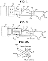
- Fig. 1 shows a configuration diagram of a first embodiment.
- 101 is a primary side circuit.
- 102 is a center-tapped isolation transformer configuring a transformer circuit.
- 102a is a negative terminal of the isolation transformer 102.
- 103 is a first switch element.
- 104 is a second switch element, and a rectifying circuit is configured of the first switch element 103 and the second switch element 104.
- 105 is a connection point of the first switch element 103 and the second switch element 104.
- 106 is a reactor.
- 107 is a capacitor configuring a smoothing circuit.
- 107a is a negative terminal of the capacitor 107.
- 108 is an output terminal.
- 109 is a load.
- 109a is a negative terminal of the load 109.
- 110 is a grounding surface.
- Vac is output ripple and voltage spike at the output terminal 108.
- the primary side circuit 101 has an isolated power conversion circuit such as a flyback, a half bridge, or a full bridge, is configured of a switching element or a diode formed of a Si semiconductor such as a MOSFET or an IGBT or a wide-bandgap semiconductor of SiC, GaN, or the like, a capacitor, and a reactor, and is connected to a primary side winding of the isolation transformer 102.
- the primary side circuit 101 is controlled by a control circuit (not shown).
- the isolation transformer 102 has a center tap in a secondary side winding, the center tap is the negative terminal 102a, which is connected to the grounding surface 110, and the negative terminal 102a of the isolation transformer 102 is connected to the negative terminal 107a of the capacitor 107 before being connected to the grounding surface 110.
- the first switch element 103 and the second switch element 104 are connected one to each of the two ends of the secondary side winding of the isolation transformer 102, rectifying diodes are used as the first switch element 103 and the second switch element 104, and an anode terminal is connected to each.
- cathode terminals of the first switch element 103 and the second switch element 104 are connected to each other, and the connection point 105 thereof is connected to the reactor 106, and is connected to a positive terminal of the load 109.
- the capacitor 107 is connected in parallel to the load 109, and the negative terminal 107a of the capacitor 107 is connected to the negative terminal 102a of the isolation transformer 102, then connected to the grounding surface 110.
- the isolation transformer 102 and the capacitor 107 also have an integrally formed aspect 201, which is shown in Fig. 2 .
- the integrally formed article 201 is such that connection points of the negative terminal 102a of the isolation transformer 102 and the negative terminal 107a of the capacitor 107 are the same, and furthermore, a connection point of a negative terminal 201a of the integrally formed article 201 is the same. Because of this, an inductance component of a path along which both a DC current and an AC current flow can be minimized, and the effect of reducing ripple and voltage spike can be increased. Also, connecting parts and holding parts, such as a bus bar that connects the negative terminal 102a of the isolation transformer and the negative terminal 107a of the capacitor, can be reduced, which also contributes to a size reduction.
- the negative terminals are connected via a bus bar, a harness, or a substrate.
- the negative terminals being connected so that the negative terminals cross or oppose a bus bar, a harness, or a substrate 111 with respect to a positive side current path 112, as shown in Fig.
- a primary side winding of an isolation transformer 202 connected in series to the isolation transformer 102 is connected to one side of the primary side winding of the isolation transformer 102, and another side is connected to the primary side circuit 101.
- a secondary side winding of the transformer 202 connected in series has a center tap, the center tap is a negative terminal 202a connected to the grounding surface 110, and the negative terminal 202a of the isolation transformer 202 connected in series is connected to the negative terminal 102a of the isolation transformer 102 and the negative terminal 107a of the capacitor 107 before being connected to the grounding surface 110.
- a third switch element 203 and a fourth switch element 204 are connected one to each of the two ends of the secondary side winding of the isolation transformer 202 connected in series, rectifying diodes are used as the third switch element 203 and the fourth switch element 204, and an anode terminal is connected to each.
- cathode terminals of the first switch element 103, the second switch element 104, the third switch element 203, and the fourth switch element 204 are connected to each other, and a connection point 205 thereof is connected to the reactor 106.
- the negative terminal 107a of the capacitor 107 is connected to the negative terminal 202a of the isolation transformer 202 connected in series to the negative terminal 102a of the isolation transformer 102, then connected to the grounding surface 110.
- FIG. 5 there is also an aspect wherein two or more of the isolation transformer 102 are connected in parallel, which is shown in Fig. 5 .
- a primary side winding of an isolation transformer 302 connected in parallel to the isolation transformer 102 is connected to the primary side circuit 101.
- a secondary side winding of the transformer 302 connected in parallel has a center tap, the center tap is a negative terminal 302a connected to the grounding surface 110, and the negative terminal 302a of the isolation transformer 302 connected in parallel is connected to the negative terminal 102a of the isolation transformer 102 and the negative terminal 107a of the capacitor 107 before being connected to the grounding surface 110.
- first switch element 103 and the second switch element 104 are connected one to each of the two ends of the secondary side winding of the isolation transformer 302 connected in parallel, rectifying diodes are used as the first switch element 103 and the second switch element 104, and an anode terminal is connected to each.
- the negative terminal 107a of the capacitor 107 is connected to the negative terminal 302a of the isolation transformer 302 connected in parallel to the negative terminal 102a of the isolation transformer 102, then connected to the grounding surface 110.
- capacitor 107 are connected in series with respect to one isolation transformer 102, which is shown in Fig. 6 as an example in which two are connected in series.
- a second capacitor 207 connected in series to the capacitor 107 is connected to the negative terminal 107a of the capacitor 107, and a negative terminal 207a of the second capacitor 207 connected in series is connected to the negative terminal 102a of the isolation transformer 102, then connected to the grounding surface 110.
- capacitor 107 are connected in parallel with respect to one isolation transformer 102, which is shown in Fig. 7 as an example in which two are connected in parallel.
- a third capacitor 307 is connected in parallel to the capacitor 107, and a negative terminal 307a of the third capacitor 307 connected in parallel is connected to the negative terminal 102a of the isolation transformer 102 and the negative terminal 107a of the capacitor 107, then connected to the grounding surface 110. Because of this, a parasitic inductance component of a capacitor through which only an AC current flows is halved, because of which a ripple current flowing to each capacitor can be reduced, while further increasing the effect of reducing output ripple and voltage spike.
- capacities of the two or more capacitors are of differing capacity values, and can be adjusted to capacities responding to a multiple of frequency components included in output ripple and a voltage spike, because of which noise can be reduced.
- This kind of configuration is such that when supplying power to the load 109 to date, a DC current (Idc) supplies power to the load 109 from the positive terminal of the isolation transformer 102 via a smoothing circuit, flows along the grounding surface 110, which forms a return path, from the negative terminal 109a of the load 109, and returns to the negative terminal 102a of the transformer. That is, the grounding surface 110 forms a return path of the DC current (Idc) supplied to the load 109.
- a DC current (Idc) supplies power to the load 109 from the positive terminal of the isolation transformer 102 via a smoothing circuit, flows along the grounding surface 110, which forms a return path, from the negative terminal 109a of the load 109, and returns to the negative terminal 102a of the transformer. That is, the grounding surface 110 forms a return path of the DC current (Idc) supplied to the load 109.
- an AC current (Iac) flows into the capacitor 107 from the positive terminal of the isolation transformer 102, flows along the grounding surface 110, which forms a return path, from the negative terminal 107a of the capacitor 107, and returns to the negative terminal 102a of the isolation transformer 102, and at this time, the return path of the AC current along the grounding surface 110 is a path of low impedance, therefore differing from the return path of the DC current along the grounding surface 110, because of which, owing to an effect of an inductance component (Lp1) in the grounding surface 110 along which only the AC current flows, the voltage Vac in accordance with the AC current (Iac) and the inductance component (Lp1) is generated. Because of this, an output ripple and a voltage spike at an output terminal of the relevant component are such that the amount of Vac increases.
- the first embodiment of the invention is such that the AC current (Iac) flowing into a capacitor always flows via the negative terminal of the capacitor into a path along which the DC current (Idc) flows, because of which a current path along which only Iac flows is of a minimum length, and an inductance component in the path of Iac decreases, because of which ripple and the voltage spike (Vac) at the output terminal can be reduced.
- FIG. 9 An example of output ripple and voltage spike waveforms of the existing form and the invention is as shown in Fig. 9 .
- a waveform A represents an output ripple and voltage spike waveform of the invention
- a waveform B represents an output ripple and voltage spike waveform of the existing form.
- both a synchronous voltage fluctuation and a spike-form fluctuation caused by switching become smaller.
- the center tap of the secondary side winding of the isolation transformer 102 is connected to the negative terminal of a capacitor before being connected to the grounding surface, but in a second embodiment, the center tap of the secondary side winding of the isolation transformer 102 is connected to the reactor 106, as shown in Fig. 10 .
- the cathode terminals of the first switch element 103 and the second switch element 104 are connected one to each of the two ends of the secondary side winding of the isolation transformer 102.
- the anode terminals of the first switch element 103 and the second switch element 104 are connected to each other, and the connection point 105 thereof is connected to the negative terminal 107a of the capacitor 107 before being connected to the grounding surface 110, which differs from the first embodiment.
- the isolation transformer 102 and the capacitor 107 also have the aspect 201, which is an integrally formed configuration and is shown in Fig. 11 .
- the integrally formed article 201 is such that the connection point 105 of the anode terminals of the first switch element 103 and the second switch element 104, the negative terminal 107a of the capacitor 107, and furthermore, the connection point of the negative terminal 201a of the integrally formed article 201, are the same. Because of this, an inductance component of a path along which both a DC current and an AC current flow can be minimized, and the effect of reducing ripple and voltage spike can be increased.
- connecting parts and holding parts such as a bus bar that connects the connection point 105 of the anode terminals of the first switch element 103 and the second switch element 104 and the negative terminal 107a of the capacitor, can be eliminated, which also contributes to a size reduction.
- connection point 105 of the first switch element 103 and the second switch element 104 and the negative terminal 107a of the capacitor 107 there is an aspect wherein connection is carried out via a bus bar, a harness, or a substrate, and by the negative terminals being connected so that the negative terminals cross or oppose a bus bar, a harness, or the substrate 111 with respect to the positive side current path 112, as shown in Fig.
- connection point of the switch elements and the negative terminal 107a of the capacitor 107 are directly connected, and by the bus bar, the harness, or the substrate 111 connecting the negative terminals being eliminated, an inductance component of a path along which both a DC current and an AC current flow can be minimized, and the effect of reducing ripple and voltage spike can be increased, while realizing a reduction in size and a reduction in cost.
- An actual connection is as shown in Fig. 12B .
- the isolation transformer 102 are connected in series, which is shown in Fig. 13 .
- One side of the primary side winding of the isolation transformer 202 connected in series to the isolation transformer 102 is connected to one side of the primary side winding of the isolation transformer 102, and the other side is connected to the primary side circuit 101.
- the secondary side winding of the transformer 202 connected in series has a center tap, and the center tap is connected to the reactor 106.
- the third switch element 203 and the fourth switch element 204 are connected one to each of the two ends of the secondary side of the transformer connected in series, rectifying diodes are used as the third switch element 203 and the fourth switch element 204, and a cathode terminal is connected to each.
- anode terminals of the first switch element 103, the second switch element 104, the third switch element 203, and the fourth switch element 204 are connected to each other, and the connection point 205 thereof is connected to the negative terminal 107a of the capacitor 107.
- the negative terminal 107a of the capacitor 107 is connected to the connection point 205, then connected to the grounding surface 110.
- the primary side winding of the isolation transformer 302 connected in parallel to the isolation transformer 102 is connected to the primary side circuit 101.
- the secondary side winding of the transformer 302 connected in parallel has a center tap, and the center tap is connected to the reactor 106.
- the first switch element 103 and the second switch element 104 are connected one to each of the two ends of the secondary side winding of the isolation transformer 302 connected in parallel, rectifying diodes are used as the first switch element 103 and the second switch element 104, and a cathode terminal is connected to each.
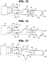
- FIG. 15 there is also an aspect wherein two or more of the capacitor 107 are connected in series with respect to one isolation transformer 102, which is shown in Fig. 15 as an example in which two are connected in series.
- the second capacitor 207 connected in series to the capacitor 107 is connected to the negative terminal 107a of the capacitor 107, and the negative terminal 207a of the second capacitor 207 connected in series is connected to the negative terminal 102a of the isolation transformer 102, then connected to the grounding surface 110.
- capacitor 107 are connected in parallel with respect to one isolation transformer 102, which is shown in Fig. 16 as an example in which two are connected in parallel.
- the third capacitor 307 is connected in parallel to the capacitor 107, and the negative terminal 307a of the third capacitor 307 connected in parallel is connected to the negative terminal 102a of the isolation transformer 102 and the negative terminal 107a of the capacitor 107, then connected to the grounding surface 110. Because of this, a parasitic inductance component of a capacitor through which only an AC current flows is halved, because of which a ripple current flowing to each capacitor can be reduced, while further increasing the effect of reducing output ripple and voltage spike.
- capacities of the two or more capacitors are of differing capacity values, and can be adjusted to capacities responding to a multiple of frequency components included in output ripple and a voltage spike, because of which noise can be reduced.
- the invention is such that the AC current (Iac) flowing into the capacitor 107 always flows via the negative terminal 107a of the capacitor 107 into a path along which the DC current (Idc) flows, because of which a current path along which only Iac flows is of a minimum length, and an inductance component in the path of Iac decreases, because of which ripple and the voltage spike (Vac) at the output terminal can be reduced.
- the negative terminal 102a of the isolation transformer 102 is connected to the negative terminal 107a of the capacitor 107 before being connected to the grounding surface 110, but in a third embodiment, the negative terminal 102a of the isolation transformer 102 is connected directly to the grounding surface 110, as shown in Fig. 17 .
- the negative terminal 107a of the capacitor 107 is connected to the negative terminal 109a of the load 109 before being connected to the grounding surface 110, which differs from the circuit of Fig. 1 .
- the isolation transformer 102 and the capacitor 107 also have the aspect 201, which is an integrally formed configuration and is shown in Fig. 18 .
- Connection points of the negative terminal 102a of the isolation transformer 102, the negative terminal 107a of the capacitor 107, the negative terminal 201a of the integrally formed article 201, and furthermore, the grounding surface 110, are the same. Because of this, an inductance component of a path along which both a DC current and an AC current flow can be minimized, and the effect of reducing ripple and voltage spike can be increased.
- the negative terminals are connected via a bus bar, a harness, or a substrate.
- the negative terminals being connected so that the negative terminals cross or oppose a bus bar, a harness, or the substrate 111 with respect to the positive side current path 112, as shown in Fig.
- FIG. 20 there is also an aspect wherein two or more of the isolation transformer 102 are connected in series, which is shown in Fig. 20 .
- One side of the primary side winding of the isolation transformer 202 connected in series to the isolation transformer 102 is connected to one side of the primary side winding of the isolation transformer 102, and the other side is connected to the primary side circuit 101.
- the secondary side winding of the transformer 202 connected in series has a center tap, the center tap is the negative terminal 202a connected to the grounding surface 110, and the negative terminal 202a of the isolation transformer 202 connected in series is connected to the grounding surface 110.
- the third switch element 203 and the fourth switch element 204 are connected one to each of the two ends of the secondary side winding of the isolation transformer 202 connected in series, rectifying diodes are used as the third switch element 203 and the fourth switch element 204, and an anode terminal is connected to each. Also, cathode terminals of the first switch element 103, the second switch element 104, the third switch element 203, and the fourth switch element 204 are connected to each other, and the connection point 205 thereof is connected to the reactor 106.
- FIG. 21 there is also an aspect wherein two or more of the isolation transformer are connected in parallel, which is shown in Fig. 21 .
- the primary side winding of the isolation transformer 302 connected in parallel to the isolation transformer 102 is connected to the primary side circuit 101.
- the secondary side winding of the transformer 302 connected in parallel has a center tap, the center tap is the negative terminal 302a connected to the grounding surface 110, and the negative terminal 302a of the isolation transformer 302 connected in parallel is connected to the negative terminal 102a of the transformer 102 and the grounding surface 110.
- first switch element 103 and the second switch element 104 are connected one to each of the two ends of the secondary side winding of the isolation transformer 302 connected in parallel, rectifying diodes are used as the first switch element 103 and the second switch element 104, and an anode terminal is connected to each.
- heat generated by a transformer will become a problem due to a further increase in power density, but a current capacity per transformer can be reduced owing to this configuration, and a particular advantage is obtained against an increase in ripple and voltage spike accompanying an increase in power density, while reducing heat generated by a transformer.
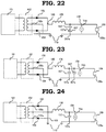
- capacitor 107 are connected in series with respect to one isolation transformer 102, which is shown in Fig. 22 as an example in which two are connected in series.
- the second capacitor 207 connected in series to the capacitor 107 is connected to the negative terminal 107a of the capacitor 107, and the negative terminal 207a of the second capacitor 207 connected in series is connected to the negative terminal 109a of the load 109, then connected to the grounding surface 110.
- the capacitor 107 are connected in parallel with respect to one isolation transformer 102, which is shown in Fig. 23 as an example in which two are connected in parallel.
- the third capacitor 307 is connected in parallel to the capacitor 107, and the negative terminal 307a of the third capacitor 307 connected in parallel is connected to the negative terminal 107a of the capacitor 107 and the negative terminal 109a of the load 109, then connected to the grounding surface 110. Because of this, a parasitic inductance component of a capacitor through which only an AC current flows is halved, because of which a ripple current flowing to each capacitor can be reduced, while further increasing the effect of reducing output ripple and voltage spike.
- capacities of the two or more capacitors are of differing capacity values, and can be adjusted to capacities responding to a multiple of frequency components included in output ripple and voltage spike, because of which noise can be reduced.
- the invention is such that the AC current (Iac) flowing into the capacitor 107 always flows via the negative terminal 107a of the capacitor 107 into a path along which the DC current (Idc) flows, because of which a current path along which only Iac flows is shortest, and an inductance component in the path of Iac decreases. Because of this, ripple and the voltage spike (Vac) at the output terminal can be reduced.
- the center tap of the secondary side winding of the isolation transformer 102 is connected to the negative terminal 107a of the capacitor 107 before being connected to the grounding surface 110, but in a fourth embodiment, the center tap of the secondary side winding of the isolation transformer 102 is connected to the reactor 106, as shown in Fig. 24 .
- the cathode terminals of the first switch element 103 and the second switch element 104 are connected one to each of the two ends of the secondary side winding of the isolation transformer 102.
- the anode terminals of the first switch element 103 and the second switch element 104 are connected to each other, and the connection point 105 thereof is connected to the grounding surface 110.
- the negative terminal 107a of the capacitor 107 is connected to the negative terminal 109a of the load 109 before being connected to the grounding surface 110, which differs from the circuit of Fig. 1 .
- the first switch element 103 and the second switch element 104 may be connected directly to the grounding surface 110, without passing through a connection point of the switch elements.
- the isolation transformer 102 and the capacitor 107 also have an aspect that is an integrally formed configuration, which is shown in Fig. 25 .
- the integrally formed article 201 is such that the connection point 105 of the anode terminals of the first switch element 103 and the second switch element 104, and the connection points of the negative terminal 107a of the capacitor 107, the negative terminal 201a of the integrally formed article 201, and furthermore, the grounding surface 110, are the same. Because of this, an inductance component of a path along which both a DC current and an AC current flow can be minimized, and the effect of reducing ripple and voltage spike can be increased.
- the negative terminals are connected via a bus bar, a harness, or a substrate.
- the negative terminals being connected so that the negative terminals cross or oppose a bus bar, a harness, or the substrate 111 with respect to the positive side current path 112, as shown in Fig.
- FIG. 26 there is also an aspect wherein two or more of the isolation transformer 102 are connected in series, which is shown in Fig. 26 .
- One side of the primary side winding of the isolation transformer 202 connected in series to the isolation transformer 102 is connected to one side of the primary side winding of the isolation transformer 102, and the other side is connected to the primary side circuit 101.
- the secondary side winding of the transformer 202 connected in series has a center tap, and the center tap is connected to the reactor 106.
- the third switch element 203 and the fourth switch element 204 are connected one to each of the two ends of the secondary side of the transformer connected in series, rectifying diodes are used as the third switch element 203 and the fourth switch element 204, and a cathode terminal is connected to each.
- anode terminals of the first switch element 103, the second switch element 104, the third switch element 203, and the fourth switch element 204 are connected to each other, and the connection point 205 thereof is connected to the grounding surface 110.
- heat generated by a transformer will become a problem due to a further increase in power density, but a number of turns per transformer can be distributed owing to this configuration, and a particular advantage is obtained against an increase in ripple and voltage spike accompanying an increase in power density, while reducing heat generated by a transformer due to a winding.
- the isolation transformer 102 are connected in parallel, which is shown in Fig. 27 .
- the primary side winding of the isolation transformer 302 connected in parallel to the isolation transformer 102 is connected to the primary side circuit 101.
- the secondary side winding of the transformer 302 connected in parallel has a center tap, and the center tap is connected to the reactor 106.
- the first switch element 103 and the second switch element 104 are connected one to each of the two ends of the secondary side winding of the isolation transformer 302 connected in parallel, rectifying diodes are used as the first switch element 103 and the second switch element 104, and a cathode terminal is connected to each.
- FIG. 28 there is also an aspect wherein two or more of the capacitor 107 are connected in series with respect to one isolation transformer 102, which is shown in Fig. 28 as an example in which two are connected in series.
- the second capacitor 207 connected in series to the capacitor 107 is connected to the negative terminal 107a of the capacitor 107, and the negative terminal 207a of the second capacitor 207 connected in series is connected to the negative terminal 109a of the load 109, then connected to the grounding surface 110.
- capacitor 107 are connected in parallel with respect to one isolation transformer 102, which is shown in Fig. 29 as an example in which two are connected in parallel.
- the third capacitor 307 is connected in parallel to the capacitor 107, and the negative terminal 307a of the third capacitor 307 connected in parallel is connected to the negative terminal 109a of the load 109 and the negative terminal 107a of the capacitor 107, then connected to the grounding surface 110. Because of this, a parasitic inductance component of a capacitor through which only an AC current flows is halved, because of which a ripple current flowing to each capacitor can be reduced, while further increasing the effect of reducing output ripple and voltage spike.
- capacities of the two or more capacitors 107 are of differing capacity values, and can be adjusted to capacities responding to a multiple of frequency components included in output ripple and voltage spike, because of which noise can be reduced.
- the invention is such that the AC current (Iac) flowing into the capacitor 107 always flows via the negative terminal 107a of the capacitor 107 into a path along which the DC current (Idc) flows, because of which a current path along which only Iac flows is shortest, and an inductance component in the path of Iac decreases, because of which ripple and the voltage spike (Vac) at the output terminal can be reduced.
- rectifying diodes are used as the first switch element 103 and the second switch element 104 connected to the isolation transformer 102, but when embodying the invention, another semiconductor switch element may be connected, and caused to operate in the same way using on/off control. Also, the reactor 106 need not necessarily be used.
- a higher frequency drive can be carried out in each of the embodiments by using wide-bandgap semiconductors as a switch element used in the primary side circuit 101, and the first switch element 103 and the second switch element 104 connected to the secondary side winding of the isolation transformer 102, a high frequency component fc included in a pulse rise time tr also increases in accompaniment to the increase in frequency, as shown in Fig. 30 , because of which an output ripple and a voltage spike of the high frequency component increase.
Landscapes
- Engineering & Computer Science (AREA)
- Power Engineering (AREA)
- Dc-Dc Converters (AREA)
- Rectifiers (AREA)
- Power Conversion In General (AREA)
Abstract
Description
- The present invention relates to a power conversion device, and in particular, relates to a power conversion device having a center-tapped isolation transformer, a rectifying circuit formed of a semiconductor switch element, and a smoothing circuit formed of a capacitor.
- An electric vehicle or a hybrid vehicle, in the same way as a vehicle that moves using an engine, includes an auxiliary battery for a control circuit that causes an electrical component to operate. However, there is no engine forming a driving source in an electric vehicle, and a start-stop system (a system such that an engine is automatically stopped when a vehicle temporarily stops, such as when waiting for lights to change at an intersection) for improving fuel economy and reducing exhaust gas is employed in a hybrid vehicle, because of which an alternator cannot be used. Because of this, a power conversion device, such as a step-down converter, that supplies energy from a driving battery that causes a travel motor to operate to an auxiliary battery, is needed in an electric vehicle or a hybrid vehicle.
- Further, a positive side and a negative side of the driving battery are both isolated from a chassis, while a negative side of a load is grounded at the chassis, because of which insulation is needed between an input and an output of the power conversion device. Herein, there is a characteristic in that the input and the output can be isolated in a device in which an isolation transformer is used.
- Integrating an input choke coil and an output choke coil, which are magnetic parts, with an isolation transformer, winding a primary coil and a secondary coil of the isolation transformer and the input and output choke coils around the same core, reducing core capacity by reducing an amount of direct current-biased magnetization of the core in a direction canceling a direct current magnetic flux created by each coil, and achieving increased efficiency by reducing core loss, has been proposed as technology using an isolation transformer, wherein full-wave rectification is carried out using a center tap of the isolation transformer, thereby realizing increased efficiency and a reduction in size (refer to Patent Document 1).
- Patent Document 1:
Japanese Patent No. 4,151,014 - A configuration such that a negative terminal of an isolation transformer, a negative terminal of a capacitor, and a negative terminal of a load (an auxiliary battery, an electric component, or the like) connected to a secondary side of the isolation transformer are connected to a grounding surface, which is a metal frame, is employed in the power conversion device proposed in Patent Document 1.
- This kind of configuration is such that to date, when carrying out a supply of power to a load, a DC current (Idc) supplies power to the load from a positive terminal of the isolation transformer via a smoothing circuit, flows along a grounding surface, which forms a return path from the negative terminal of the load, and returns to the negative terminal of the isolation transformer. An AC current (Iac) flows into the capacitor from the positive terminal of the isolation transformer, flows along a grounding surface, which forms a return path, from the negative terminal of the capacitor, and returns to the negative terminal of the isolation transformer, but at this time, the return path of the AC current along the grounding surface is a path of low impedance, differing from the return path of the DC current along the grounding surface, because of which, owing to an effect of an inductance component (Lp1) in the grounding surface along which only the AC current flows, a voltage Vac in accordance with the AC current (Iac) and the inductance component (Lp1) is generated. Because of this, there is a problem in that an output ripple and a voltage spike at an output terminal of the relevant component are such that the amount of Vac increases.
- Technology such that an input choke coil, an output choke coil, and a transformer, which are magnetic parts, are inserted in order to control output ripple voltage and ripple current, and the inserted magnetic parts can be reduced in size, is introduced in Patent Document 1.
- However, as there is no task for further reducing ripple and spike in the circuit configuration, there is a problem in that an increase in ripple and voltage spike occurs.
- The invention has an object of providing a circuit configuration that restricts output ripple and spike in a power conversion device having a transformer circuit formed of a center-tapped isolation transformer, a rectifying circuit formed of a semiconductor switch element, and a smoothing circuit formed of a capacitor.
- A transformer circuit formed of a center-tapped isolation transformer, a rectifying circuit formed of a semiconductor switch element connected to the transformer circuit, a smoothing circuit formed of a capacitor connected to the rectifying circuit, a positive terminal and a negative terminal connected to a load, and a grounding surface to which the negative terminal is connected, are included as a circuit configuration that restricts output ripple and spike, wherein a negative terminal of the isolation transformer and a negative terminal of the capacitor are connected before being connected to the grounding surface, or the negative terminal connected to the load and the negative terminal of the capacitor are connected before being connected to the grounding surface. Advantageous Effects of Invention
- According to the invention, a negative terminal of an isolation transformer and a negative terminal of a capacitor are connected before being connected to a grounding surface, or a negative terminal connected to a load and the negative terminal of the capacitor are connected before being connected to the grounding surface, because of which a current path along which only an AC current flows can be shortened, and output ripple and a voltage spike at an output terminal can be reduced.
-
-
Fig. 1 is a schematic configuration diagram showing a power conversion device according to a first embodiment of the invention. -
Fig. 2 is a schematic configuration diagram showing the power conversion device according to the first embodiment of the invention. -
Fig. 3A is a schematic configuration diagram showing a connection configuration of the first embodiment of the invention. -
Fig. 3B is a schematic configuration diagram showing a connection configuration of the first embodiment of the invention. -
Fig. 4 is a schematic configuration diagram showing the power conversion device according to the first embodiment of the invention. -
Fig. 5 is a schematic configuration diagram showing the power conversion device according to the first embodiment of the invention. -
Fig. 6 is a schematic configuration diagram showing the power conversion device according to the first embodiment of the invention. -
Fig. 7 is a schematic configuration diagram showing the power conversion device according to the first embodiment of the invention. -
Fig. 8 is an equivalent circuit diagram showing an inductance componence of a grounding surface along which an AC current flows in an existing DC-DC converter shown for comparison. -
Fig. 9 is a waveform diagram showing a state of an output ripple and a voltage spike of a device having the configuration of the first embodiment of the invention and an existing device. -
Fig. 10 is a schematic configuration diagram showing a power conversion device according to a second embodiment of the invention. -
Fig. 11 is a schematic configuration diagram showing the power conversion device according to the second embodiment of the invention. -
Fig. 12A is a schematic configuration diagram showing a connection configuration of the second embodiment of the invention. -
Fig. 12B is a schematic configuration diagram showing a connection configuration of the second embodiment of the invention. -
Fig. 13 is a schematic configuration diagram showing the power conversion device according to the second embodiment of the invention. -
Fig. 14 is a schematic configuration diagram showing the power conversion device according to the second embodiment of the invention. -
Fig. 15 is a schematic configuration diagram showing the power conversion device according to the second embodiment of the invention. -
Fig. 16 is a schematic configuration diagram showing the power conversion device according to the second embodiment of the invention. -
Fig. 17 is a schematic configuration diagram showing a power conversion device according to a third embodiment of the invention. -
Fig. 18 is a schematic configuration diagram showing the power conversion device according to the third embodiment of the invention. -
Fig. 19A is a schematic configuration diagram showing a connection configuration of the third embodiment of the invention. -
Fig. 19B is a schematic configuration diagram showing a connection configuration of the third embodiment of the invention. -
Fig. 20 is a schematic configuration diagram showing the power conversion device according to the third embodiment of the invention. -
Fig. 21 is a schematic configuration diagram showing the power conversion device according to the third embodiment of the invention. -
Fig. 22 is a schematic configuration diagram showing the power conversion device according to the third embodiment of the invention. -
Fig. 23 is a schematic configuration diagram showing the power conversion device according to the third embodiment of the invention. -
Fig. 24 is a schematic configuration diagram showing a power conversion device according to a fourth embodiment of the invention. -
Fig. 25 is a schematic configuration diagram showing the power conversion device according to the fourth embodiment of the invention. -
Fig. 26 is a schematic configuration diagram showing the power conversion device according to the fourth embodiment of the invention. -
Fig. 27 is a schematic configuration diagram showing the power conversion device according to the fourth embodiment of the invention. -
Fig. 28 is a schematic configuration diagram showing the power conversion device according to the fourth embodiment of the invention. -
Fig. 29 is a schematic configuration diagram showing the power conversion device according to the fourth embodiment of the invention. -
Fig. 30 is a high frequency characteristic diagram of when the invention is applied to a power conversion device in which a wide-bandgap semiconductor is adopted as a switch element. - Hereafter, using the drawings, preferred embodiments of a power conversion device according to the invention will be described, but the same reference signs will be allotted to identical or corresponding portions in the drawings, and a redundant description will be omitted.
-
Fig. 1 shows a configuration diagram of a first embodiment. 101 is a primary side circuit. 102 is a center-tapped isolation transformer configuring a transformer circuit. 102a is a negative terminal of theisolation transformer 102. 103 is a first switch element. 104 is a second switch element, and a rectifying circuit is configured of thefirst switch element 103 and thesecond switch element 104. 105 is a connection point of thefirst switch element 103 and thesecond switch element 104. 106 is a reactor. 107 is a capacitor configuring a smoothing circuit. 107a is a negative terminal of thecapacitor 107. 108 is an output terminal. 109 is a load. 109a is a negative terminal of theload 109. 110 is a grounding surface. Vac is output ripple and voltage spike at theoutput terminal 108. - The
primary side circuit 101 has an isolated power conversion circuit such as a flyback, a half bridge, or a full bridge, is configured of a switching element or a diode formed of a Si semiconductor such as a MOSFET or an IGBT or a wide-bandgap semiconductor of SiC, GaN, or the like, a capacitor, and a reactor, and is connected to a primary side winding of theisolation transformer 102. Theprimary side circuit 101 is controlled by a control circuit (not shown). - The
isolation transformer 102 has a center tap in a secondary side winding, the center tap is thenegative terminal 102a, which is connected to thegrounding surface 110, and the negative terminal 102a of theisolation transformer 102 is connected to the negative terminal 107a of thecapacitor 107 before being connected to thegrounding surface 110. Also, thefirst switch element 103 and thesecond switch element 104 are connected one to each of the two ends of the secondary side winding of theisolation transformer 102, rectifying diodes are used as thefirst switch element 103 and thesecond switch element 104, and an anode terminal is connected to each. Also, cathode terminals of thefirst switch element 103 and thesecond switch element 104 are connected to each other, and theconnection point 105 thereof is connected to thereactor 106, and is connected to a positive terminal of theload 109. Next, thecapacitor 107 is connected in parallel to theload 109, and the negative terminal 107a of thecapacitor 107 is connected to the negative terminal 102a of theisolation transformer 102, then connected to thegrounding surface 110. - The
isolation transformer 102 and thecapacitor 107 also have an integrally formedaspect 201, which is shown inFig. 2 . The integrally formedarticle 201 is such that connection points of the negative terminal 102a of theisolation transformer 102 and the negative terminal 107a of thecapacitor 107 are the same, and furthermore, a connection point of a negative terminal 201a of the integrally formedarticle 201 is the same. Because of this, an inductance component of a path along which both a DC current and an AC current flow can be minimized, and the effect of reducing ripple and voltage spike can be increased. Also, connecting parts and holding parts, such as a bus bar that connects the negative terminal 102a of the isolation transformer and the negative terminal 107a of the capacitor, can be reduced, which also contributes to a size reduction. - Next, as a method of connecting the negative terminal 102a of the
isolation transformer 102 and the negative terminal 107a of thecapacitor 107, there is an aspect wherein the negative terminals are connected via a bus bar, a harness, or a substrate. By the negative terminals being connected so that the negative terminals cross or oppose a bus bar, a harness, or asubstrate 111 with respect to a positive sidecurrent path 112, as shown inFig. 3A , mutual inductance is reduced by a magnetic field Hf generated by current flowing to a smoothing circuit positive side and a magnetic field Hr generated by current flowing to the bus bar, the harness, or thesubstrate 111 connecting the negative terminals being canceled, because of which an inductance component of a path along which both a DC current and an AC current flow can be reduced, and the effect of reducing ripple and voltage spike can be increased. Furthermore, there is also an aspect wherein the negative terminals are directly connected, and by the bus bar, the harness, or thesubstrate 111 connecting the negative terminals being eliminated, an inductance component of a path along which both a DC current and an AC current flow can be minimized, and the effect of reducing ripple and voltage spike can be increased, while realizing a reduction in size and a reduction in cost. An actual connection is as shown inFig. 3B . - Next, there is also an aspect wherein two or more of the
isolation transformer 102 are connected in series, which is shown inFig. 4 . One side of a primary side winding of anisolation transformer 202 connected in series to theisolation transformer 102 is connected to one side of the primary side winding of theisolation transformer 102, and another side is connected to theprimary side circuit 101. Also, a secondary side winding of thetransformer 202 connected in series has a center tap, the center tap is anegative terminal 202a connected to thegrounding surface 110, and the negative terminal 202a of theisolation transformer 202 connected in series is connected to the negative terminal 102a of theisolation transformer 102 and the negative terminal 107a of thecapacitor 107 before being connected to thegrounding surface 110. Also, athird switch element 203 and afourth switch element 204 are connected one to each of the two ends of the secondary side winding of theisolation transformer 202 connected in series, rectifying diodes are used as thethird switch element 203 and thefourth switch element 204, and an anode terminal is connected to each. Also, cathode terminals of thefirst switch element 103, thesecond switch element 104, thethird switch element 203, and thefourth switch element 204 are connected to each other, and aconnection point 205 thereof is connected to thereactor 106. Next, the negative terminal 107a of thecapacitor 107 is connected to the negative terminal 202a of theisolation transformer 202 connected in series to the negative terminal 102a of theisolation transformer 102, then connected to thegrounding surface 110. In future, heat generated by a transformer will become a problem due to a further increase in power density, but a number of turns per transformer can be distributed owing to this configuration, and a particular advantage is obtained against an increase in ripple and voltage spike accompanying an increase in power density, while reducing heat generated by a transformer due to a winding. - Next, there is also an aspect wherein two or more of the
isolation transformer 102 are connected in parallel, which is shown inFig. 5 . A primary side winding of anisolation transformer 302 connected in parallel to theisolation transformer 102 is connected to theprimary side circuit 101. Also, a secondary side winding of thetransformer 302 connected in parallel has a center tap, the center tap is anegative terminal 302a connected to thegrounding surface 110, and the negative terminal 302a of theisolation transformer 302 connected in parallel is connected to the negative terminal 102a of theisolation transformer 102 and the negative terminal 107a of thecapacitor 107 before being connected to thegrounding surface 110. Also, thefirst switch element 103 and thesecond switch element 104 are connected one to each of the two ends of the secondary side winding of theisolation transformer 302 connected in parallel, rectifying diodes are used as thefirst switch element 103 and thesecond switch element 104, and an anode terminal is connected to each. Next, the negative terminal 107a of thecapacitor 107 is connected to the negative terminal 302a of theisolation transformer 302 connected in parallel to the negative terminal 102a of theisolation transformer 102, then connected to thegrounding surface 110. In future, heat generated by a transformer will become a problem due to a further increase in power density, but a current capacity per transformer can be reduced owing to this configuration, and a particular advantage is obtained against an increase in ripple and voltage spike accompanying an increase in power density, while reducing heat generated by a transformer. - Next, there is also an aspect wherein two or more of the
capacitor 107 are connected in series with respect to oneisolation transformer 102, which is shown inFig. 6 as an example in which two are connected in series. Asecond capacitor 207 connected in series to thecapacitor 107 is connected to the negative terminal 107a of thecapacitor 107, and a negative terminal 207a of thesecond capacitor 207 connected in series is connected to the negative terminal 102a of theisolation transformer 102, then connected to thegrounding surface 110. Because of this, voltage applied to one of the capacitors can be lowered, and furthermore, although a parasitic inductance component of a capacitor through which only an AC current flows doubles in return for a short-circuit failure between the output terminal and grounding surface being preventable even when one of the two capacitors fails when a failure mode of the capacitors used is a short-circuit mode, an increase in output ripple and voltage spike can be kept to a minimum by adopting the configuration ofFig. 6 . - Also, there is also an aspect wherein two or more of the
capacitor 107 are connected in parallel with respect to oneisolation transformer 102, which is shown inFig. 7 as an example in which two are connected in parallel. Athird capacitor 307 is connected in parallel to thecapacitor 107, and a negative terminal 307a of thethird capacitor 307 connected in parallel is connected to the negative terminal 102a of theisolation transformer 102 and the negative terminal 107a of thecapacitor 107, then connected to thegrounding surface 110. Because of this, a parasitic inductance component of a capacitor through which only an AC current flows is halved, because of which a ripple current flowing to each capacitor can be reduced, while further increasing the effect of reducing output ripple and voltage spike. - Furthermore, there is also an aspect wherein capacities of the two or more capacitors are of differing capacity values, and can be adjusted to capacities responding to a multiple of frequency components included in output ripple and a voltage spike, because of which noise can be reduced.
- As opposed to the configurations shown in the first embodiment, a configuration such that the negative terminal 102a of the
isolation transformer 102 connected to the secondary side of theisolation transformer 102, the negative terminal 107a of thecapacitor 107, and the negative terminal 109a of the load 109 (for example, an auxiliary battery, an electric component, or the like), are connected to thegrounding surface 110, which is a metal frame, is adopted in an existing device, as shown inFig. 8 for comparison purposes. - This kind of configuration is such that when supplying power to the
load 109 to date, a DC current (Idc) supplies power to theload 109 from the positive terminal of theisolation transformer 102 via a smoothing circuit, flows along thegrounding surface 110, which forms a return path, from the negative terminal 109a of theload 109, and returns to the negative terminal 102a of the transformer. That is, thegrounding surface 110 forms a return path of the DC current (Idc) supplied to theload 109. - Consequently, an AC current (Iac) flows into the
capacitor 107 from the positive terminal of theisolation transformer 102, flows along thegrounding surface 110, which forms a return path, from the negative terminal 107a of thecapacitor 107, and returns to the negative terminal 102a of theisolation transformer 102, and at this time, the return path of the AC current along thegrounding surface 110 is a path of low impedance, therefore differing from the return path of the DC current along thegrounding surface 110, because of which, owing to an effect of an inductance component (Lp1) in thegrounding surface 110 along which only the AC current flows, the voltage Vac in accordance with the AC current (Iac) and the inductance component (Lp1) is generated. Because of this, an output ripple and a voltage spike at an output terminal of the relevant component are such that the amount of Vac increases. - As opposed to this, the first embodiment of the invention is such that the AC current (Iac) flowing into a capacitor always flows via the negative terminal of the capacitor into a path along which the DC current (Idc) flows, because of which a current path along which only Iac flows is of a minimum length, and an inductance component in the path of Iac decreases, because of which ripple and the voltage spike (Vac) at the output terminal can be reduced.
- An example of output ripple and voltage spike waveforms of the existing form and the invention is as shown in
Fig. 9 . - In
Fig. 9 , a waveform A represents an output ripple and voltage spike waveform of the invention, and a waveform B represents an output ripple and voltage spike waveform of the existing form. As shown inFig. 9 , both a synchronous voltage fluctuation and a spike-form fluctuation caused by switching become smaller. - A range of application of the invention not being limited to the circuit configuration shown in
Fig. 1 as the first embodiment, various kinds of modification can be carried out, as shown as differing embodiments by modified examples of the circuit inFig. 10 to Fig. 29 . - In the first embodiment, the center tap of the secondary side winding of the
isolation transformer 102 is connected to the negative terminal of a capacitor before being connected to the grounding surface, but in a second embodiment, the center tap of the secondary side winding of theisolation transformer 102 is connected to thereactor 106, as shown inFig. 10 . Next, the cathode terminals of thefirst switch element 103 and thesecond switch element 104 are connected one to each of the two ends of the secondary side winding of theisolation transformer 102. Also, the anode terminals of thefirst switch element 103 and thesecond switch element 104 are connected to each other, and theconnection point 105 thereof is connected to the negative terminal 107a of thecapacitor 107 before being connected to thegrounding surface 110, which differs from the first embodiment. - The
isolation transformer 102 and thecapacitor 107 also have theaspect 201, which is an integrally formed configuration and is shown inFig. 11 . The integrally formedarticle 201 is such that theconnection point 105 of the anode terminals of thefirst switch element 103 and thesecond switch element 104, the negative terminal 107a of thecapacitor 107, and furthermore, the connection point of the negative terminal 201a of the integrally formedarticle 201, are the same. Because of this, an inductance component of a path along which both a DC current and an AC current flow can be minimized, and the effect of reducing ripple and voltage spike can be increased. Also, connecting parts and holding parts, such as a bus bar that connects theconnection point 105 of the anode terminals of thefirst switch element 103 and thesecond switch element 104 and the negative terminal 107a of the capacitor, can be eliminated, which also contributes to a size reduction. - Next, as a method of connecting the
connection point 105 of thefirst switch element 103 and thesecond switch element 104 and the negative terminal 107a of thecapacitor 107, there is an aspect wherein connection is carried out via a bus bar, a harness, or a substrate, and by the negative terminals being connected so that the negative terminals cross or oppose a bus bar, a harness, or thesubstrate 111 with respect to the positive sidecurrent path 112, as shown inFig. 12A , mutual inductance is reduced by the magnetic field Hf generated by current flowing to the smoothing circuit positive side and the magnetic field Hr generated by current flowing to the bus bar, the harness, or thesubstrate 111 connecting the negative terminals being canceled, because of which an inductance component of a path along which both a DC current and an AC current flow can be reduced, and the effect of reducing ripple and voltage spike can be increased. Furthermore, there is also an aspect wherein the connection point of the switch elements and the negative terminal 107a of thecapacitor 107 are directly connected, and by the bus bar, the harness, or thesubstrate 111 connecting the negative terminals being eliminated, an inductance component of a path along which both a DC current and an AC current flow can be minimized, and the effect of reducing ripple and voltage spike can be increased, while realizing a reduction in size and a reduction in cost. An actual connection is as shown inFig. 12B . - Next, there is also an aspect wherein two or more of the
isolation transformer 102 are connected in series, which is shown inFig. 13 . One side of the primary side winding of theisolation transformer 202 connected in series to theisolation transformer 102 is connected to one side of the primary side winding of theisolation transformer 102, and the other side is connected to theprimary side circuit 101. Also, the secondary side winding of thetransformer 202 connected in series has a center tap, and the center tap is connected to thereactor 106. Next, thethird switch element 203 and thefourth switch element 204 are connected one to each of the two ends of the secondary side of the transformer connected in series, rectifying diodes are used as thethird switch element 203 and thefourth switch element 204, and a cathode terminal is connected to each. Also, anode terminals of thefirst switch element 103, thesecond switch element 104, thethird switch element 203, and thefourth switch element 204 are connected to each other, and theconnection point 205 thereof is connected to the negative terminal 107a of thecapacitor 107. Next, the negative terminal 107a of thecapacitor 107 is connected to theconnection point 205, then connected to thegrounding surface 110. In future, heat generated by a transformer will become a problem due to a further increase in power density, but a number of turns per transformer can be distributed owing to this configuration, and a particular advantage is obtained against an increase in ripple and voltage spike accompanying an increase in power density, while reducing heat generated by a transformer due to a winding. - Next, there is also an aspect wherein two or more of the
isolation transformer 102 are connected in parallel, which is shown inFig. 14 . The primary side winding of theisolation transformer 302 connected in parallel to theisolation transformer 102 is connected to theprimary side circuit 101. Also, the secondary side winding of thetransformer 302 connected in parallel has a center tap, and the center tap is connected to thereactor 106. Also, thefirst switch element 103 and thesecond switch element 104 are connected one to each of the two ends of the secondary side winding of theisolation transformer 302 connected in parallel, rectifying diodes are used as thefirst switch element 103 and thesecond switch element 104, and a cathode terminal is connected to each. In future, heat generated by a transformer will become a problem due to a further increase in power density, but a current capacity per transformer can be reduced owing to this configuration, and a particular advantage is obtained against an increase in ripple and voltage spike accompanying an increase in power density, while reducing heat generated by a transformer. - Next, there is also an aspect wherein two or more of the
capacitor 107 are connected in series with respect to oneisolation transformer 102, which is shown inFig. 15 as an example in which two are connected in series. Thesecond capacitor 207 connected in series to thecapacitor 107 is connected to the negative terminal 107a of thecapacitor 107, and the negative terminal 207a of thesecond capacitor 207 connected in series is connected to the negative terminal 102a of theisolation transformer 102, then connected to thegrounding surface 110. Because of this, voltage applied to one of the capacitors can be lowered, and furthermore, although a parasitic inductance component of a capacitor through which only an AC current flows doubles in return for a short-circuit failure between the output terminal and grounding surface being preventable even when one of the two capacitors fails when a failure mode of the capacitors used is a short-circuit mode, an increase in output ripple and voltage spike can be kept to a minimum by adopting this configuration. - Also, there is also an aspect wherein two or more of the
capacitor 107 are connected in parallel with respect to oneisolation transformer 102, which is shown inFig. 16 as an example in which two are connected in parallel. Thethird capacitor 307 is connected in parallel to thecapacitor 107, and the negative terminal 307a of thethird capacitor 307 connected in parallel is connected to the negative terminal 102a of theisolation transformer 102 and the negative terminal 107a of thecapacitor 107, then connected to thegrounding surface 110. Because of this, a parasitic inductance component of a capacitor through which only an AC current flows is halved, because of which a ripple current flowing to each capacitor can be reduced, while further increasing the effect of reducing output ripple and voltage spike. - Furthermore, there is also an aspect wherein capacities of the two or more capacitors are of differing capacity values, and can be adjusted to capacities responding to a multiple of frequency components included in output ripple and a voltage spike, because of which noise can be reduced.
- The invention is such that the AC current (Iac) flowing into the
capacitor 107 always flows via the negative terminal 107a of thecapacitor 107 into a path along which the DC current (Idc) flows, because of which a current path along which only Iac flows is of a minimum length, and an inductance component in the path of Iac decreases, because of which ripple and the voltage spike (Vac) at the output terminal can be reduced. - In the first embodiment, the negative terminal 102a of the
isolation transformer 102 is connected to the negative terminal 107a of thecapacitor 107 before being connected to thegrounding surface 110, but in a third embodiment, the negative terminal 102a of theisolation transformer 102 is connected directly to thegrounding surface 110, as shown inFig. 17 . Next, the negative terminal 107a of thecapacitor 107 is connected to the negative terminal 109a of theload 109 before being connected to thegrounding surface 110, which differs from the circuit ofFig. 1 . - The
isolation transformer 102 and thecapacitor 107 also have theaspect 201, which is an integrally formed configuration and is shown inFig. 18 . Connection points of the negative terminal 102a of theisolation transformer 102, the negative terminal 107a of thecapacitor 107, the negative terminal 201a of the integrally formedarticle 201, and furthermore, thegrounding surface 110, are the same. Because of this, an inductance component of a path along which both a DC current and an AC current flow can be minimized, and the effect of reducing ripple and voltage spike can be increased. - Next, as a method of connecting the negative terminal 107a of the
capacitor 107 and the negative terminal 109a of theload 109, there is an aspect wherein the negative terminals are connected via a bus bar, a harness, or a substrate. By the negative terminals being connected so that the negative terminals cross or oppose a bus bar, a harness, or thesubstrate 111 with respect to the positive sidecurrent path 112, as shown inFig. 19A , mutual inductance is reduced by the magnetic field Hf generated by current flowing to the smoothing circuit positive side and the magnetic field Hr generated by current flowing to the bus bar, the harness, or thesubstrate 111 connecting the negative terminals being canceled, because of which an inductance component of a path along which both a DC current and an AC current flow can be reduced, and the effect of reducing ripple and voltage spike can be increased. Furthermore, there is also an aspect wherein the negative terminals are directly connected, and by the bus bar, the harness, or thesubstrate 111 connecting the negative terminals being eliminated, an inductance component of a path along which both a DC current and an AC current flow can be minimized, and the effect of reducing ripple and voltage spike can be increased, while realizing a reduction in size and a reduction in cost. An actual connection is as shown inFig. 19B . - Next, there is also an aspect wherein two or more of the
isolation transformer 102 are connected in series, which is shown inFig. 20 . One side of the primary side winding of theisolation transformer 202 connected in series to theisolation transformer 102 is connected to one side of the primary side winding of theisolation transformer 102, and the other side is connected to theprimary side circuit 101. Also, the secondary side winding of thetransformer 202 connected in series has a center tap, the center tap is thenegative terminal 202a connected to thegrounding surface 110, and the negative terminal 202a of theisolation transformer 202 connected in series is connected to thegrounding surface 110. Also, thethird switch element 203 and thefourth switch element 204 are connected one to each of the two ends of the secondary side winding of theisolation transformer 202 connected in series, rectifying diodes are used as thethird switch element 203 and thefourth switch element 204, and an anode terminal is connected to each. Also, cathode terminals of thefirst switch element 103, thesecond switch element 104, thethird switch element 203, and thefourth switch element 204 are connected to each other, and theconnection point 205 thereof is connected to thereactor 106. In future, heat generated by a transformer will become a problem due to a further increase in power density, but a number of turns per transformer can be distributed owing to this configuration, and a particular advantage is obtained against an increase in ripple and voltage spike accompanying an increase in power density, while reducing heat generated by a transformer due to a winding. - Also, there is also an aspect wherein two or more of the isolation transformer are connected in parallel, which is shown in
Fig. 21 . The primary side winding of theisolation transformer 302 connected in parallel to theisolation transformer 102 is connected to theprimary side circuit 101. Also, the secondary side winding of thetransformer 302 connected in parallel has a center tap, the center tap is thenegative terminal 302a connected to thegrounding surface 110, and the negative terminal 302a of theisolation transformer 302 connected in parallel is connected to the negative terminal 102a of thetransformer 102 and thegrounding surface 110. Also, thefirst switch element 103 and thesecond switch element 104 are connected one to each of the two ends of the secondary side winding of theisolation transformer 302 connected in parallel, rectifying diodes are used as thefirst switch element 103 and thesecond switch element 104, and an anode terminal is connected to each. In future, heat generated by a transformer will become a problem due to a further increase in power density, but a current capacity per transformer can be reduced owing to this configuration, and a particular advantage is obtained against an increase in ripple and voltage spike accompanying an increase in power density, while reducing heat generated by a transformer. - Next, there is also an aspect wherein two or more of the
capacitor 107 are connected in series with respect to oneisolation transformer 102, which is shown inFig. 22 as an example in which two are connected in series. Thesecond capacitor 207 connected in series to thecapacitor 107 is connected to the negative terminal 107a of thecapacitor 107, and the negative terminal 207a of thesecond capacitor 207 connected in series is connected to the negative terminal 109a of theload 109, then connected to thegrounding surface 110. Because of this, voltage applied to one of the capacitors can be lowered, and although a parasitic inductance component of a capacitor through which only an AC current flows doubles in return for a short-circuit failure between the output terminal and grounding surface being preventable even when one of the two capacitors fails when a failure mode of the capacitors used is a short-circuit mode, an increase in output ripple and voltage spike can be kept to a minimum by adopting this configuration. - Also, there is also an aspect wherein two or more of the
capacitor 107 are connected in parallel with respect to oneisolation transformer 102, which is shown inFig. 23 as an example in which two are connected in parallel. Thethird capacitor 307 is connected in parallel to thecapacitor 107, and the negative terminal 307a of thethird capacitor 307 connected in parallel is connected to the negative terminal 107a of thecapacitor 107 and the negative terminal 109a of theload 109, then connected to thegrounding surface 110. Because of this, a parasitic inductance component of a capacitor through which only an AC current flows is halved, because of which a ripple current flowing to each capacitor can be reduced, while further increasing the effect of reducing output ripple and voltage spike. - Furthermore, there is also an aspect wherein capacities of the two or more capacitors are of differing capacity values, and can be adjusted to capacities responding to a multiple of frequency components included in output ripple and voltage spike, because of which noise can be reduced.
- The invention is such that the AC current (Iac) flowing into the
capacitor 107 always flows via the negative terminal 107a of thecapacitor 107 into a path along which the DC current (Idc) flows, because of which a current path along which only Iac flows is shortest, and an inductance component in the path of Iac decreases. Because of this, ripple and the voltage spike (Vac) at the output terminal can be reduced. - In the first embodiment, the center tap of the secondary side winding of the
isolation transformer 102 is connected to the negative terminal 107a of thecapacitor 107 before being connected to thegrounding surface 110, but in a fourth embodiment, the center tap of the secondary side winding of theisolation transformer 102 is connected to thereactor 106, as shown inFig. 24 . Next, the cathode terminals of thefirst switch element 103 and thesecond switch element 104 are connected one to each of the two ends of the secondary side winding of theisolation transformer 102. Also, the anode terminals of thefirst switch element 103 and thesecond switch element 104 are connected to each other, and theconnection point 105 thereof is connected to thegrounding surface 110. Next, the negative terminal 107a of thecapacitor 107 is connected to the negative terminal 109a of theload 109 before being connected to thegrounding surface 110, which differs from the circuit ofFig. 1 . Thefirst switch element 103 and thesecond switch element 104 may be connected directly to thegrounding surface 110, without passing through a connection point of the switch elements. - The
isolation transformer 102 and thecapacitor 107 also have an aspect that is an integrally formed configuration, which is shown inFig. 25 . The integrally formedarticle 201 is such that theconnection point 105 of the anode terminals of thefirst switch element 103 and thesecond switch element 104, and the connection points of the negative terminal 107a of thecapacitor 107, the negative terminal 201a of the integrally formedarticle 201, and furthermore, thegrounding surface 110, are the same. Because of this, an inductance component of a path along which both a DC current and an AC current flow can be minimized, and the effect of reducing ripple and voltage spike can be increased. - Next, as a method of connecting the negative terminal 107a of the
capacitor 107 and the negative terminal 109a of theload 109, there is an aspect wherein the negative terminals are connected via a bus bar, a harness, or a substrate. By the negative terminals being connected so that the negative terminals cross or oppose a bus bar, a harness, or thesubstrate 111 with respect to the positive sidecurrent path 112, as shown inFig. 19A , mutual inductance is reduced by the magnetic field Hf generated by current flowing to the smoothing circuit positive side and the magnetic field Hr generated by current flowing to the bus bar, the harness, or thesubstrate 111 connecting the negative terminals being canceled, because of which an inductance component of a path along which both a DC current and an AC current flow can be reduced, and the effect of reducing ripple and voltage spike can be increased. Furthermore, there is also an aspect wherein the negative terminals are directly connected, and by the bus bar, the harness, or thesubstrate 111 connecting the negative terminals being eliminated, an inductance component of a path along which both a DC current and an AC current flow can be minimized, and the effect of reducing ripple and voltage spike can be increased, while realizing a reduction in size and a reduction in cost. An actual connection is as shown inFig. 19B . - Next, there is also an aspect wherein two or more of the
isolation transformer 102 are connected in series, which is shown inFig. 26 . One side of the primary side winding of theisolation transformer 202 connected in series to theisolation transformer 102 is connected to one side of the primary side winding of theisolation transformer 102, and the other side is connected to theprimary side circuit 101. Also, the secondary side winding of thetransformer 202 connected in series has a center tap, and the center tap is connected to thereactor 106. Next, thethird switch element 203 and thefourth switch element 204 are connected one to each of the two ends of the secondary side of the transformer connected in series, rectifying diodes are used as thethird switch element 203 and thefourth switch element 204, and a cathode terminal is connected to each. Also, anode terminals of thefirst switch element 103, thesecond switch element 104, thethird switch element 203, and thefourth switch element 204 are connected to each other, and theconnection point 205 thereof is connected to thegrounding surface 110. In future, heat generated by a transformer will become a problem due to a further increase in power density, but a number of turns per transformer can be distributed owing to this configuration, and a particular advantage is obtained against an increase in ripple and voltage spike accompanying an increase in power density, while reducing heat generated by a transformer due to a winding. - Also, there is also an aspect wherein two or more of the
isolation transformer 102 are connected in parallel, which is shown inFig. 27 . The primary side winding of theisolation transformer 302 connected in parallel to theisolation transformer 102 is connected to theprimary side circuit 101. Also, the secondary side winding of thetransformer 302 connected in parallel has a center tap, and the center tap is connected to thereactor 106. Also, thefirst switch element 103 and thesecond switch element 104 are connected one to each of the two ends of the secondary side winding of theisolation transformer 302 connected in parallel, rectifying diodes are used as thefirst switch element 103 and thesecond switch element 104, and a cathode terminal is connected to each. In future, heat generated by a transformer will become a problem due to a further increase in power density, but a current capacity per transformer can be reduced owing to this configuration, because of which a particular advantage is obtained against an increase in ripple and voltage spike accompanying an increase in power density, while reducing heat generated by a transformer. - Next, there is also an aspect wherein two or more of the
capacitor 107 are connected in series with respect to oneisolation transformer 102, which is shown inFig. 28 as an example in which two are connected in series. Thesecond capacitor 207 connected in series to thecapacitor 107 is connected to the negative terminal 107a of thecapacitor 107, and the negative terminal 207a of thesecond capacitor 207 connected in series is connected to the negative terminal 109a of theload 109, then connected to thegrounding surface 110. Because of this, voltage applied to one of the capacitors can be lowered, and although a parasitic inductance component of a capacitor through which only an AC current flows doubles in return for a short-circuit failure between the output terminal and thegrounding surface 110 being preventable even when one of the two capacitors fails when a failure mode of the capacitors used is a short-circuit mode, an increase in output ripple and voltage spike can be kept to a minimum by adopting this configuration. - Also, there is also an aspect wherein two or more of the
capacitor 107 are connected in parallel with respect to oneisolation transformer 102, which is shown inFig. 29 as an example in which two are connected in parallel. Thethird capacitor 307 is connected in parallel to thecapacitor 107, and the negative terminal 307a of thethird capacitor 307 connected in parallel is connected to the negative terminal 109a of theload 109 and the negative terminal 107a of thecapacitor 107, then connected to thegrounding surface 110. Because of this, a parasitic inductance component of a capacitor through which only an AC current flows is halved, because of which a ripple current flowing to each capacitor can be reduced, while further increasing the effect of reducing output ripple and voltage spike. - Furthermore, there is also an aspect wherein capacities of the two or
more capacitors 107 are of differing capacity values, and can be adjusted to capacities responding to a multiple of frequency components included in output ripple and voltage spike, because of which noise can be reduced. - The invention is such that the AC current (Iac) flowing into the
capacitor 107 always flows via the negative terminal 107a of thecapacitor 107 into a path along which the DC current (Idc) flows, because of which a current path along which only Iac flows is shortest, and an inductance component in the path of Iac decreases, because of which ripple and the voltage spike (Vac) at the output terminal can be reduced. - In each of the embodiments, rectifying diodes are used as the
first switch element 103 and thesecond switch element 104 connected to theisolation transformer 102, but when embodying the invention, another semiconductor switch element may be connected, and caused to operate in the same way using on/off control. Also, thereactor 106 need not necessarily be used. - Also, although a higher frequency drive can be carried out in each of the embodiments by using wide-bandgap semiconductors as a switch element used in the
primary side circuit 101, and thefirst switch element 103 and thesecond switch element 104 connected to the secondary side winding of theisolation transformer 102, a high frequency component fc included in a pulse rise time tr also increases in accompaniment to the increase in frequency, as shown inFig. 30 , because of which an output ripple and a voltage spike of the high frequency component increase. In particular, as the high frequency component is considerably affected by a parasitic inductance of L*di/dt, a particular advantage is obtained in reducing the output ripple and the voltage spike of the high frequency component by applying the invention to a power conversion device in which wide-bandgap semiconductors are used as the switch elements, because of which the invention is convenient when wide-bandgap semiconductors are applied to the switch elements. - The embodiments can be freely combined, and arbitrary components of the embodiments can be changed or abbreviated as appropriate, without departing from the scope of the invention.
Claims (14)
- A power conversion device, comprising:a transformer circuit formed of a center-tapped isolation transformer;a rectifying circuit formed of a semiconductor switch element connected to the transformer circuit;a smoothing circuit formed of a capacitor connected to the rectifying circuit;a positive terminal and a negative terminal connected to a load; anda grounding surface to which the negative terminal of the load is connected, whereina negative terminal of the isolation transformer and a negative terminal of the capacitor are connected before being connected to the grounding surface, or the negative terminal of the capacitor and the negative terminal connected to the load are connected before being connected to the grounding surface.
- The power conversion device according to claim 1, wherein the capacitor and the isolation transformer are integrally formed.
- The power conversion device according to claim 1 or 2, wherein there are two or more of the isolation transformer.
- The power conversion device according to claim 1 or 2, wherein two or more of the capacitor are connected with respect to one of the isolation transformer.
- The power conversion device according to claim 1 or 2, wherein the negative terminal of the isolation transformer and the negative terminal of the capacitor, or the negative terminal of the capacitor and the negative terminal connected to the load, are directly connected.
- The power conversion device according to claim 1 or 2, wherein the negative terminal of the isolation transformer and the negative terminal of the capacitor, or the negative terminal of the capacitor and the negative terminal connected to the load, are connected via a bus bar.
- The power conversion device according to claim 1 or 2, wherein the negative terminal of the isolation transformer and the negative terminal of the capacitor, or the negative terminal of the capacitor and the negative terminal connected to the load, are connected via a harness.
- The power conversion device according to claim 1 or 2, wherein the negative terminal of the isolation transformer and the negative terminal of the capacitor, or the negative terminal of the capacitor and the negative terminal connected to the load, are connected via a substrate pattern.
- The power conversion device according to claim 3, wherein two or more of the isolation transformer are connected in series.
- The power conversion device according to claim 3, wherein two or more of the isolation transformer are connected in parallel.
- The power conversion device according to claim 4, wherein two or more of the capacitor are connected in series.
- The power conversion device according to claim 4, wherein two or more of the capacitor are connected in parallel.
- The power conversion device according to claim 11 or 12, wherein two or more of the capacitor are configured of differing capacities.
- The power conversion device according to any one of claims 1 to 13, wherein the semiconductor switch element is a wide-bandgap semiconductor.
Applications Claiming Priority (1)
| Application Number | Priority Date | Filing Date | Title |
|---|---|---|---|
| PCT/JP2016/081672 WO2018078734A1 (en) | 2016-10-26 | 2016-10-26 | Power conversion device |
Publications (3)
| Publication Number | Publication Date |
|---|---|
| EP3534519A1 true EP3534519A1 (en) | 2019-09-04 |
| EP3534519A4 EP3534519A4 (en) | 2019-11-06 |
| EP3534519B1 EP3534519B1 (en) | 2022-06-01 |
Family
ID=62024522
Family Applications (1)
| Application Number | Title | Priority Date | Filing Date |
|---|---|---|---|
| EP16919803.3A Active EP3534519B1 (en) | 2016-10-26 | 2016-10-26 | Power conversion device |
Country Status (5)
| Country | Link |
|---|---|
| US (1) | US11431259B2 (en) |
| EP (1) | EP3534519B1 (en) |
| JP (1) | JPWO2018078734A1 (en) |
| CN (1) | CN109891731A (en) |
| WO (1) | WO2018078734A1 (en) |
Families Citing this family (3)
| Publication number | Priority date | Publication date | Assignee | Title |
|---|---|---|---|---|
| JP6879436B2 (en) * | 2018-10-04 | 2021-06-02 | 三菱電機株式会社 | Power supply and magnetic resonance imaging |
| JP7314835B2 (en) * | 2020-02-28 | 2023-07-26 | Tdk株式会社 | Transformers, power converters, and power conversion systems |
| JP7098025B1 (en) * | 2021-06-09 | 2022-07-08 | 三菱電機株式会社 | Power converter |
Family Cites Families (24)
| Publication number | Priority date | Publication date | Assignee | Title |
|---|---|---|---|---|
| US4053815A (en) * | 1973-09-10 | 1977-10-11 | Federal Pacific Electric Company | Ground fault interrupters |
| US4017784A (en) * | 1976-05-17 | 1977-04-12 | Litton Systems, Inc. | DC to DC converter |
| JPS6477474A (en) * | 1987-09-16 | 1989-03-23 | Toshiba Electric Equip | Molded transformer |
| JPH06205581A (en) * | 1992-12-25 | 1994-07-22 | Hitachi Lighting Ltd | Power supply |
| US5666255A (en) * | 1995-06-05 | 1997-09-09 | Powervar, Inc. | Transformerless conditioning of a power distribution system |
| JP2003023773A (en) * | 2001-07-05 | 2003-01-24 | Toyota Industries Corp | Power supply unit |
| JP4151014B2 (en) | 2003-03-11 | 2008-09-17 | 株式会社デンソー | Isolated switching DC / DC converter |
| JP2008178205A (en) * | 2007-01-18 | 2008-07-31 | Densei Lambda Kk | Switching power supply |
| JP2009142088A (en) * | 2007-12-07 | 2009-06-25 | Hitachi Ltd | DC-DC converter for display device |
| EP2190109B1 (en) | 2008-10-27 | 2014-09-03 | STMicroelectronics Srl | Control device for rectifiers of switching converters. |
| JP2010246316A (en) * | 2009-04-08 | 2010-10-28 | Toyota Motor Corp | Smoothing circuit |
| US20100284203A1 (en) | 2009-05-11 | 2010-11-11 | Intersil Americas Inc. | Control mode for zvs converter at resonant operating frequencies |
| CN101599698A (en) * | 2009-05-19 | 2009-12-09 | 广州金升阳科技有限公司 | A kind of micro-power DC-DC power supply and manufacture method thereof |
| CN201789412U (en) * | 2010-08-25 | 2011-04-06 | 国琏电子(上海)有限公司 | Power supply system |
| CN201947186U (en) * | 2011-03-04 | 2011-08-24 | 山东大学 | Main circuit of current feed type high-power high-frequency high-voltage switching power supply |
| JP2013247814A (en) * | 2012-05-28 | 2013-12-09 | Toyota Industries Corp | Power supply device |
| JP5894909B2 (en) * | 2012-12-13 | 2016-03-30 | 日立オートモティブシステムズ株式会社 | DC-DC converter device |
| JPWO2015053139A1 (en) | 2013-10-07 | 2017-03-09 | 日立オートモティブシステムズ株式会社 | Power converter |
| US9350260B2 (en) * | 2013-11-07 | 2016-05-24 | Futurewei Technologies, Inc. | Startup method and system for resonant converters |
| JP6158051B2 (en) * | 2013-11-29 | 2017-07-05 | 日立オートモティブシステムズ株式会社 | Power converter |
| CN204068683U (en) * | 2014-09-04 | 2014-12-31 | 永济新时速电机电器有限责任公司 | A kind of capacitance group of efficient low sense and install the power cell of this capacitance group |
| JP6451620B2 (en) * | 2015-12-18 | 2019-01-16 | 株式会社デンソー | Power supply |
| CN205544914U (en) * | 2015-12-29 | 2016-08-31 | 苏州松田微电子有限公司 | Low -cost filter circuit |
| CN105958812B (en) * | 2016-06-15 | 2018-05-11 | 维沃移动通信有限公司 | Switching power circuit and the method debugged to switching power circuit |
-
2016
- 2016-10-26 CN CN201680090227.7A patent/CN109891731A/en active Pending
- 2016-10-26 WO PCT/JP2016/081672 patent/WO2018078734A1/en not_active Ceased
- 2016-10-26 US US16/343,508 patent/US11431259B2/en active Active
- 2016-10-26 JP JP2018546981A patent/JPWO2018078734A1/en active Pending
- 2016-10-26 EP EP16919803.3A patent/EP3534519B1/en active Active
Also Published As
| Publication number | Publication date |
|---|---|
| US11431259B2 (en) | 2022-08-30 |
| EP3534519B1 (en) | 2022-06-01 |
| JPWO2018078734A1 (en) | 2018-12-20 |
| US20210281188A1 (en) | 2021-09-09 |
| WO2018078734A1 (en) | 2018-05-03 |
| EP3534519A4 (en) | 2019-11-06 |
| CN109891731A (en) | 2019-06-14 |
Similar Documents
| Publication | Publication Date | Title |
|---|---|---|
| US9025345B2 (en) | Power supply apparatus | |
| KR101628133B1 (en) | A Pulse Width Modulation Resonance Converter and Charger for Vehicle Using the Same | |
| JP5855133B2 (en) | Charger | |
| US8659272B2 (en) | Bidirectional boost-buck DC-DC converter | |
| JP5642245B1 (en) | Car charger | |
| CN105981278A (en) | In-vehicle charger and surge-suppression method for in-vehicle charger | |
| KR20110110805A (en) | DC / DC Converters and AC / DC Converters | |
| JP2015159711A (en) | Switching power supply, power converter | |
| US9866135B2 (en) | Power conversion device including primary inverter, transformer, secondary converter | |
| US9866129B2 (en) | Power conversion device including primary inverter, transformer, secondary converter, and controller | |
| KR20160122441A (en) | Charging device of vehicle | |
| US20060007717A1 (en) | Switching power supply with direct conversion off AC power source | |
| CN104247242B (en) | The output stage of charging equipment | |
| JPH0417567A (en) | Switching power supply circuit | |
| US20220294338A1 (en) | Charger for in plug-in electric vehicles | |
| US11431259B2 (en) | Power conversion device for reducing voltage ripple and voltage spike via connection of a transformer and a capacitor to a grounding surface | |
| CN114649949A (en) | High-capacity bidirectional isolation type direct current-direct current converter and control method thereof | |
| US12160176B2 (en) | Power converter | |
| Hou et al. | Low-voltage electrical systems for nonpropulsion loads | |
| US7656683B2 (en) | Electrical conversion device, converter and uninterruptible electric power supply comprising one such device | |
| CN108141137A (en) | DC converter and method for operating a DC converter | |
| JP2015139312A (en) | Switching power supply, power converter | |
| JP7752453B1 (en) | DC-DC converter overvoltage suppression control circuit | |
| HK1252510A1 (en) | Electric power converter with snubber circuit | |
| JP2026011370A (en) | Control method for current-source DC-DC converters |
Legal Events
| Date | Code | Title | Description |
|---|---|---|---|
| STAA | Information on the status of an ep patent application or granted ep patent |
Free format text: STATUS: THE INTERNATIONAL PUBLICATION HAS BEEN MADE |
|
| PUAI | Public reference made under article 153(3) epc to a published international application that has entered the european phase |
Free format text: ORIGINAL CODE: 0009012 |
|
| STAA | Information on the status of an ep patent application or granted ep patent |
Free format text: STATUS: REQUEST FOR EXAMINATION WAS MADE |
|
| 17P | Request for examination filed |
Effective date: 20190403 |
|
| AK | Designated contracting states |
Kind code of ref document: A1 Designated state(s): AL AT BE BG CH CY CZ DE DK EE ES FI FR GB GR HR HU IE IS IT LI LT LU LV MC MK MT NL NO PL PT RO RS SE SI SK SM TR |
|
| AX | Request for extension of the european patent |
Extension state: BA ME |
|
| REG | Reference to a national code |
Ref country code: DE Ref legal event code: R079 Ref document number: 602016072617 Country of ref document: DE Free format text: PREVIOUS MAIN CLASS: H02M0003280000 Ipc: H02M0003335000 |
|
| A4 | Supplementary search report drawn up and despatched |
Effective date: 20191008 |
|
| RIC1 | Information provided on ipc code assigned before grant |
Ipc: H02M 3/335 20060101AFI20191001BHEP Ipc: H02M 1/00 20060101ALI20191001BHEP Ipc: H02M 7/00 20060101ALI20191001BHEP |
|
| DAV | Request for validation of the european patent (deleted) | ||
| DAX | Request for extension of the european patent (deleted) | ||
| STAA | Information on the status of an ep patent application or granted ep patent |
Free format text: STATUS: EXAMINATION IS IN PROGRESS |
|
| 17Q | First examination report despatched |
Effective date: 20201009 |
|
| GRAP | Despatch of communication of intention to grant a patent |
Free format text: ORIGINAL CODE: EPIDOSNIGR1 |
|
| STAA | Information on the status of an ep patent application or granted ep patent |
Free format text: STATUS: GRANT OF PATENT IS INTENDED |
|
| INTG | Intention to grant announced |
Effective date: 20220302 |
|
| GRAS | Grant fee paid |
Free format text: ORIGINAL CODE: EPIDOSNIGR3 |
|
| GRAA | (expected) grant |
Free format text: ORIGINAL CODE: 0009210 |
|
| STAA | Information on the status of an ep patent application or granted ep patent |
Free format text: STATUS: THE PATENT HAS BEEN GRANTED |
|
| AK | Designated contracting states |
Kind code of ref document: B1 Designated state(s): AL AT BE BG CH CY CZ DE DK EE ES FI FR GB GR HR HU IE IS IT LI LT LU LV MC MK MT NL NO PL PT RO RS SE SI SK SM TR |
|
| REG | Reference to a national code |
Ref country code: GB Ref legal event code: FG4D |
|
| REG | Reference to a national code |
Ref country code: AT Ref legal event code: REF Ref document number: 1496079 Country of ref document: AT Kind code of ref document: T Effective date: 20220615 Ref country code: CH Ref legal event code: EP Ref country code: DE Ref legal event code: R096 Ref document number: 602016072617 Country of ref document: DE |
|
| REG | Reference to a national code |
Ref country code: IE Ref legal event code: FG4D |
|
| REG | Reference to a national code |
Ref country code: LT Ref legal event code: MG9D |
|
| REG | Reference to a national code |
Ref country code: NL Ref legal event code: MP Effective date: 20220601 |
|
| PG25 | Lapsed in a contracting state [announced via postgrant information from national office to epo] |
Ref country code: SE Free format text: LAPSE BECAUSE OF FAILURE TO SUBMIT A TRANSLATION OF THE DESCRIPTION OR TO PAY THE FEE WITHIN THE PRESCRIBED TIME-LIMIT Effective date: 20220601 Ref country code: NO Free format text: LAPSE BECAUSE OF FAILURE TO SUBMIT A TRANSLATION OF THE DESCRIPTION OR TO PAY THE FEE WITHIN THE PRESCRIBED TIME-LIMIT Effective date: 20220901 Ref country code: LT Free format text: LAPSE BECAUSE OF FAILURE TO SUBMIT A TRANSLATION OF THE DESCRIPTION OR TO PAY THE FEE WITHIN THE PRESCRIBED TIME-LIMIT Effective date: 20220601 Ref country code: HR Free format text: LAPSE BECAUSE OF FAILURE TO SUBMIT A TRANSLATION OF THE DESCRIPTION OR TO PAY THE FEE WITHIN THE PRESCRIBED TIME-LIMIT Effective date: 20220601 Ref country code: GR Free format text: LAPSE BECAUSE OF FAILURE TO SUBMIT A TRANSLATION OF THE DESCRIPTION OR TO PAY THE FEE WITHIN THE PRESCRIBED TIME-LIMIT Effective date: 20220902 Ref country code: FI Free format text: LAPSE BECAUSE OF FAILURE TO SUBMIT A TRANSLATION OF THE DESCRIPTION OR TO PAY THE FEE WITHIN THE PRESCRIBED TIME-LIMIT Effective date: 20220601 Ref country code: ES Free format text: LAPSE BECAUSE OF FAILURE TO SUBMIT A TRANSLATION OF THE DESCRIPTION OR TO PAY THE FEE WITHIN THE PRESCRIBED TIME-LIMIT Effective date: 20220601 Ref country code: BG Free format text: LAPSE BECAUSE OF FAILURE TO SUBMIT A TRANSLATION OF THE DESCRIPTION OR TO PAY THE FEE WITHIN THE PRESCRIBED TIME-LIMIT Effective date: 20220901 |
|
| REG | Reference to a national code |
Ref country code: AT Ref legal event code: MK05 Ref document number: 1496079 Country of ref document: AT Kind code of ref document: T Effective date: 20220601 |
|
| PG25 | Lapsed in a contracting state [announced via postgrant information from national office to epo] |
Ref country code: RS Free format text: LAPSE BECAUSE OF FAILURE TO SUBMIT A TRANSLATION OF THE DESCRIPTION OR TO PAY THE FEE WITHIN THE PRESCRIBED TIME-LIMIT Effective date: 20220601 Ref country code: PL Free format text: LAPSE BECAUSE OF FAILURE TO SUBMIT A TRANSLATION OF THE DESCRIPTION OR TO PAY THE FEE WITHIN THE PRESCRIBED TIME-LIMIT Effective date: 20220601 Ref country code: LV Free format text: LAPSE BECAUSE OF FAILURE TO SUBMIT A TRANSLATION OF THE DESCRIPTION OR TO PAY THE FEE WITHIN THE PRESCRIBED TIME-LIMIT Effective date: 20220601 |
|
| PG25 | Lapsed in a contracting state [announced via postgrant information from national office to epo] |
Ref country code: NL Free format text: LAPSE BECAUSE OF FAILURE TO SUBMIT A TRANSLATION OF THE DESCRIPTION OR TO PAY THE FEE WITHIN THE PRESCRIBED TIME-LIMIT Effective date: 20220601 |
|
| PG25 | Lapsed in a contracting state [announced via postgrant information from national office to epo] |
Ref country code: SM Free format text: LAPSE BECAUSE OF FAILURE TO SUBMIT A TRANSLATION OF THE DESCRIPTION OR TO PAY THE FEE WITHIN THE PRESCRIBED TIME-LIMIT Effective date: 20220601 Ref country code: SK Free format text: LAPSE BECAUSE OF FAILURE TO SUBMIT A TRANSLATION OF THE DESCRIPTION OR TO PAY THE FEE WITHIN THE PRESCRIBED TIME-LIMIT Effective date: 20220601 Ref country code: RO Free format text: LAPSE BECAUSE OF FAILURE TO SUBMIT A TRANSLATION OF THE DESCRIPTION OR TO PAY THE FEE WITHIN THE PRESCRIBED TIME-LIMIT Effective date: 20220601 Ref country code: PT Free format text: LAPSE BECAUSE OF FAILURE TO SUBMIT A TRANSLATION OF THE DESCRIPTION OR TO PAY THE FEE WITHIN THE PRESCRIBED TIME-LIMIT Effective date: 20221003 Ref country code: EE Free format text: LAPSE BECAUSE OF FAILURE TO SUBMIT A TRANSLATION OF THE DESCRIPTION OR TO PAY THE FEE WITHIN THE PRESCRIBED TIME-LIMIT Effective date: 20220601 Ref country code: CZ Free format text: LAPSE BECAUSE OF FAILURE TO SUBMIT A TRANSLATION OF THE DESCRIPTION OR TO PAY THE FEE WITHIN THE PRESCRIBED TIME-LIMIT Effective date: 20220601 Ref country code: AT Free format text: LAPSE BECAUSE OF FAILURE TO SUBMIT A TRANSLATION OF THE DESCRIPTION OR TO PAY THE FEE WITHIN THE PRESCRIBED TIME-LIMIT Effective date: 20220601 |
|
| PG25 | Lapsed in a contracting state [announced via postgrant information from national office to epo] |
Ref country code: IS Free format text: LAPSE BECAUSE OF FAILURE TO SUBMIT A TRANSLATION OF THE DESCRIPTION OR TO PAY THE FEE WITHIN THE PRESCRIBED TIME-LIMIT Effective date: 20221001 |
|
| REG | Reference to a national code |
Ref country code: DE Ref legal event code: R097 Ref document number: 602016072617 Country of ref document: DE |
|
| PG25 | Lapsed in a contracting state [announced via postgrant information from national office to epo] |
Ref country code: AL Free format text: LAPSE BECAUSE OF FAILURE TO SUBMIT A TRANSLATION OF THE DESCRIPTION OR TO PAY THE FEE WITHIN THE PRESCRIBED TIME-LIMIT Effective date: 20220601 |
|
| PLBE | No opposition filed within time limit |
Free format text: ORIGINAL CODE: 0009261 |
|
| STAA | Information on the status of an ep patent application or granted ep patent |
Free format text: STATUS: NO OPPOSITION FILED WITHIN TIME LIMIT |
|
| PG25 | Lapsed in a contracting state [announced via postgrant information from national office to epo] |
Ref country code: DK Free format text: LAPSE BECAUSE OF FAILURE TO SUBMIT A TRANSLATION OF THE DESCRIPTION OR TO PAY THE FEE WITHIN THE PRESCRIBED TIME-LIMIT Effective date: 20220601 |
|
| 26N | No opposition filed |
Effective date: 20230302 |
|
| PG25 | Lapsed in a contracting state [announced via postgrant information from national office to epo] |
Ref country code: SI Free format text: LAPSE BECAUSE OF FAILURE TO SUBMIT A TRANSLATION OF THE DESCRIPTION OR TO PAY THE FEE WITHIN THE PRESCRIBED TIME-LIMIT Effective date: 20220601 Ref country code: MC Free format text: LAPSE BECAUSE OF FAILURE TO SUBMIT A TRANSLATION OF THE DESCRIPTION OR TO PAY THE FEE WITHIN THE PRESCRIBED TIME-LIMIT Effective date: 20220601 |
|
| REG | Reference to a national code |
Ref country code: CH Ref legal event code: PL |
|
| P01 | Opt-out of the competence of the unified patent court (upc) registered |
Effective date: 20230512 |
|
| REG | Reference to a national code |
Ref country code: BE Ref legal event code: MM Effective date: 20221031 |
|
| GBPC | Gb: european patent ceased through non-payment of renewal fee |
Effective date: 20221026 |
|
| PG25 | Lapsed in a contracting state [announced via postgrant information from national office to epo] |
Ref country code: LU Free format text: LAPSE BECAUSE OF NON-PAYMENT OF DUE FEES Effective date: 20221026 |
|
| PG25 | Lapsed in a contracting state [announced via postgrant information from national office to epo] |
Ref country code: LI Free format text: LAPSE BECAUSE OF NON-PAYMENT OF DUE FEES Effective date: 20221031 Ref country code: CH Free format text: LAPSE BECAUSE OF NON-PAYMENT OF DUE FEES Effective date: 20221031 |
|
| PG25 | Lapsed in a contracting state [announced via postgrant information from national office to epo] |
Ref country code: BE Free format text: LAPSE BECAUSE OF NON-PAYMENT OF DUE FEES Effective date: 20221031 |
|
| PG25 | Lapsed in a contracting state [announced via postgrant information from national office to epo] |
Ref country code: IE Free format text: LAPSE BECAUSE OF NON-PAYMENT OF DUE FEES Effective date: 20221026 Ref country code: GB Free format text: LAPSE BECAUSE OF NON-PAYMENT OF DUE FEES Effective date: 20221026 |
|
| PG25 | Lapsed in a contracting state [announced via postgrant information from national office to epo] |
Ref country code: IT Free format text: LAPSE BECAUSE OF FAILURE TO SUBMIT A TRANSLATION OF THE DESCRIPTION OR TO PAY THE FEE WITHIN THE PRESCRIBED TIME-LIMIT Effective date: 20220601 |
|
| PG25 | Lapsed in a contracting state [announced via postgrant information from national office to epo] |
Ref country code: HU Free format text: LAPSE BECAUSE OF FAILURE TO SUBMIT A TRANSLATION OF THE DESCRIPTION OR TO PAY THE FEE WITHIN THE PRESCRIBED TIME-LIMIT; INVALID AB INITIO Effective date: 20161026 |
|
| PG25 | Lapsed in a contracting state [announced via postgrant information from national office to epo] |
Ref country code: CY Free format text: LAPSE BECAUSE OF FAILURE TO SUBMIT A TRANSLATION OF THE DESCRIPTION OR TO PAY THE FEE WITHIN THE PRESCRIBED TIME-LIMIT Effective date: 20220601 |
|
| PG25 | Lapsed in a contracting state [announced via postgrant information from national office to epo] |
Ref country code: MK Free format text: LAPSE BECAUSE OF FAILURE TO SUBMIT A TRANSLATION OF THE DESCRIPTION OR TO PAY THE FEE WITHIN THE PRESCRIBED TIME-LIMIT Effective date: 20220601 |
|
| PG25 | Lapsed in a contracting state [announced via postgrant information from national office to epo] |
Ref country code: MT Free format text: LAPSE BECAUSE OF FAILURE TO SUBMIT A TRANSLATION OF THE DESCRIPTION OR TO PAY THE FEE WITHIN THE PRESCRIBED TIME-LIMIT Effective date: 20220601 |
|
| PGFP | Annual fee paid to national office [announced via postgrant information from national office to epo] |
Ref country code: FR Payment date: 20240909 Year of fee payment: 9 |
|
| PG25 | Lapsed in a contracting state [announced via postgrant information from national office to epo] |
Ref country code: BG Free format text: LAPSE BECAUSE OF FAILURE TO SUBMIT A TRANSLATION OF THE DESCRIPTION OR TO PAY THE FEE WITHIN THE PRESCRIBED TIME-LIMIT Effective date: 20220601 |
|
| PG25 | Lapsed in a contracting state [announced via postgrant information from national office to epo] |
Ref country code: BG Free format text: LAPSE BECAUSE OF FAILURE TO SUBMIT A TRANSLATION OF THE DESCRIPTION OR TO PAY THE FEE WITHIN THE PRESCRIBED TIME-LIMIT Effective date: 20220601 |
|
| PGFP | Annual fee paid to national office [announced via postgrant information from national office to epo] |
Ref country code: DE Payment date: 20240904 Year of fee payment: 9 |
|
| PG25 | Lapsed in a contracting state [announced via postgrant information from national office to epo] |
Ref country code: TR Free format text: LAPSE BECAUSE OF FAILURE TO SUBMIT A TRANSLATION OF THE DESCRIPTION OR TO PAY THE FEE WITHIN THE PRESCRIBED TIME-LIMIT Effective date: 20220601 |