EP3534262A1 - Processing system, related integrated circuit and method - Google Patents
Processing system, related integrated circuit and method Download PDFInfo
- Publication number
- EP3534262A1 EP3534262A1 EP19159273.2A EP19159273A EP3534262A1 EP 3534262 A1 EP3534262 A1 EP 3534262A1 EP 19159273 A EP19159273 A EP 19159273A EP 3534262 A1 EP3534262 A1 EP 3534262A1
- Authority
- EP
- European Patent Office
- Prior art keywords
- error
- err
- signal
- memory
- address
- Prior art date
- Legal status (The legal status is an assumption and is not a legal conclusion. Google has not performed a legal analysis and makes no representation as to the accuracy of the status listed.)
- Granted
Links
Images




Classifications
-
- G—PHYSICS
- G06—COMPUTING OR CALCULATING; COUNTING
- G06F—ELECTRIC DIGITAL DATA PROCESSING
- G06F11/00—Error detection; Error correction; Monitoring
- G06F11/07—Responding to the occurrence of a fault, e.g. fault tolerance
- G06F11/08—Error detection or correction by redundancy in data representation, e.g. by using checking codes
- G06F11/10—Adding special bits or symbols to the coded information, e.g. parity check, casting out 9's or 11's
- G06F11/1008—Adding special bits or symbols to the coded information, e.g. parity check, casting out 9's or 11's in individual solid state devices
- G06F11/1048—Adding special bits or symbols to the coded information, e.g. parity check, casting out 9's or 11's in individual solid state devices using arrangements adapted for a specific error detection or correction feature
-
- G—PHYSICS
- G06—COMPUTING OR CALCULATING; COUNTING
- G06F—ELECTRIC DIGITAL DATA PROCESSING
- G06F11/00—Error detection; Error correction; Monitoring
- G06F11/07—Responding to the occurrence of a fault, e.g. fault tolerance
- G06F11/0703—Error or fault processing not based on redundancy, i.e. by taking additional measures to deal with the error or fault not making use of redundancy in operation, in hardware, or in data representation
- G06F11/0793—Remedial or corrective actions
-
- G—PHYSICS
- G06—COMPUTING OR CALCULATING; COUNTING
- G06F—ELECTRIC DIGITAL DATA PROCESSING
- G06F11/00—Error detection; Error correction; Monitoring
- G06F11/07—Responding to the occurrence of a fault, e.g. fault tolerance
- G06F11/0703—Error or fault processing not based on redundancy, i.e. by taking additional measures to deal with the error or fault not making use of redundancy in operation, in hardware, or in data representation
- G06F11/0706—Error or fault processing not based on redundancy, i.e. by taking additional measures to deal with the error or fault not making use of redundancy in operation, in hardware, or in data representation the processing taking place on a specific hardware platform or in a specific software environment
- G06F11/0727—Error or fault processing not based on redundancy, i.e. by taking additional measures to deal with the error or fault not making use of redundancy in operation, in hardware, or in data representation the processing taking place on a specific hardware platform or in a specific software environment in a storage system, e.g. in a DASD or network based storage system
-
- G—PHYSICS
- G06—COMPUTING OR CALCULATING; COUNTING
- G06F—ELECTRIC DIGITAL DATA PROCESSING
- G06F11/00—Error detection; Error correction; Monitoring
- G06F11/07—Responding to the occurrence of a fault, e.g. fault tolerance
- G06F11/0703—Error or fault processing not based on redundancy, i.e. by taking additional measures to deal with the error or fault not making use of redundancy in operation, in hardware, or in data representation
- G06F11/0751—Error or fault detection not based on redundancy
Definitions
- Embodiments of the present disclosure relate to processing systems, such as micro-controllers, having associated a memory.
- FIG. 1 shows a typical electronic system, such as the electronic system of a vehicle, comprising a plurality of processing systems 10, such as embedded systems or integrated circuits, e.g ., a Field Programmable Gate Array (FPGA), Digital Signal Processor (DSP) or a micro-controller (e.g ., dedicated to the automotive market).
- processing systems 10 such as embedded systems or integrated circuits, e.g ., a Field Programmable Gate Array (FPGA), Digital Signal Processor (DSP) or a micro-controller (e.g ., dedicated to the automotive market).
- FPGA Field Programmable Gate Array
- DSP Digital Signal Processor
- micro-controller e.g ., dedicated to the automotive market.
- the communication system may include a vehicle control bus, such as a Controller Area Network (CAN) bus, and possibly a multimedia bus, such as a Media Oriented Systems Transport (MOST) bus, connected to the vehicle control bus via a gateway.
- vehicle control bus such as a Controller Area Network (CAN) bus
- multimedia bus such as a Media Oriented Systems Transport (MOST) bus
- the processing systems 10 are located at different positions of the vehicle and may include, e.g ., an Engine Control Unit (ECU), a Transmission Control Unit (TCU), an Anti-lock Braking System (ABS), a body control modules (BCM), and/or a navigation and/or multimedia audio system.
- ECU Engine Control Unit
- TCU Transmission Control Unit
- ABS Anti-lock Braking System
- BCM body control modules
- Figure 2 shows a block diagram of a typical digital processing system 10 corresponding to any of the previously mentioned processing systems 10 1 , 10 2 and/or 10 3 , such as a micro-controller.
- the processing system 10 comprises at least one processing unit 102, such as a microprocessor, usually the Central Processing Unit (CPU), programmed via software instructions.
- processing unit 102 such as a microprocessor, usually the Central Processing Unit (CPU), programmed via software instructions.
- CPU Central Processing Unit
- the software executed by the processing unit 102 is stored in a non-volatile program memory 104a, such as a Flash memory or EEPROM.
- the memory 104a is configured to store the firmware for the processing unit 102, wherein the term firmware includes both the software of a micro-processor and the programming data of a programmable logic circuits, such as a FPGA.
- the processing unit 102 may have associated one or more volatile memories 104b, such as a Random-Access Memory (RAM), e.g . a Static Random-Access Memory (SRAM) or a Dynamic Random-Access Memory, e.g. for storing temporary results of the program executed by the processing unit 102.
- RAM Random-Access Memory
- SRAM Static Random-Access Memory
- Dynamic Random-Access Memory e.g. for storing temporary results of the program executed by the processing unit 102.
- each memory 104a or 104b may be integrated with the processing unit 102 in a single integrated circuit, or the memory may be in the form of a separate integrated circuit and connected to the processing unit 102, e.g . via the traces of a printed circuit board.
- processing unit 102 may have associated one or more further resources 106, such as:
- Future generation of processing systems in particular micro-controllers dedicated to automotive applications, will exhibit a significant increase in complexity, mainly due to the increasing number of functionalities (such as new protocols, new features, etc.) and to the tight constraints concerning the operation conditions of the system (such as lower power consumption, increased calculation power and speed, etc.).
- complexity is expected to increase in particular in the context of the forthcoming Car2X and autonomous driving world, because safety and security of the processing systems 10 will become more and more relevant.
- the processing units 10 should be able to detect and/or correct errors in the data read from the memories 104a and/or 104b, thereby permitting that suitable measure are taken in order to avoid malfunctions of the system.
- various embodiments of the present disclosure to provide solutions able to improve the behavior of a processing system, such as a micro-controller, in response to an error in the data read from a memory.
- one or more of the above objectives is achieved by means of a processing system having the features specifically set forth in the claims that follow.
- Embodiments moreover concern a related integrated circuit and method.
- various embodiments of the present description relate to a processing system comprising a processing unit, such as micro-processor adapted to be programmed via software instructions.
- the processing unit is arranged to be connected to a memory with error detection and/or correction, wherein the processing unit generates a read request for reading data from the memory, wherein the read request comprises an address signal identifying the address of a given memory area in the memory.
- the memory may be integrated in the processing system, e.g. in an integrated circuit, or may be connected externally to the processing system.
- the memory may be a non-volatile memory arranged to store the firmware for the processing unit and/or a Random-Access Memory arranged to store temporary results of the processing of the processing unit.
- the processing system comprises moreover an error handling circuit.
- the error handling circuit is connected to the memory for receiving an error signal from the memory.
- the error signal may contain an error code indicating whether the data read from the memory do contain errors.
- the error signal may comprise a plurality of bits, and the error code of the error signal may indicate (at least) that no error occurred during the reading operation of the data, an error occurred during the reading operation of the data, but the error was corrected, and an error occurred during the reading operation of the data and the error was not corrected.
- the error handling circuit is configured to generate (at least) a first error signal and a second error signal.
- the error handling circuit comprises a hardware circuit configured to determine whether the address indicated by the address signal belongs to a first address range and set the first error signal to the error code of the error signal when the address indicated by the address signal belongs to the first address range.
- the hardware circuit may determine whether the address indicated by the address signal belongs to a second address range and set the second error signal to the error code of the error signal when the address indicated by the address signal belongs to the second address range.
- the first address range and/or the second address range are programmable.
- the hardware circuit may comprise a first combinational logic circuit configured to set a first enable signal to a first or second logic value when the address indicated by the address signal belongs or does not belong to the first address range, respectively.
- the hardware circuit may comprise a second combinational logic circuit configured to set a second enable signal to a first or second logic value when the address indicated by the address signal belongs or does not belong to the second address range, respectively.
- the hardware circuit may also comprise a third combinational logic circuit configured to set the first error signal to the error code of the error signal when the first enable signal has the first logic value and set the second error signal to the error code of the error signal when the second enable signal has the first logic value.
- the error handling circuit may comprise moreover a register configured to store the error code of the error signal and provide the stored error code to the hardware circuit for generating the first and second error signal. Additionally or alternatively, the error handling circuit may comprise a register configured to store the error code of the first or second error signal.
- the error handling circuit has associated an interrupt generator circuit configured to generate one or more interrupt signals when the error code of the first error signal corresponds to one or more first reference values and/or the error code of the second error signal corresponds to one or more second reference values.
- the one or more first reference values and/or the one or more second reference values are programmable.
- At least one of the interrupt signals, the first error signal and the second error signal may be provided to the processing unit of the processing system.
- the processing system may comprise a communication interface and at least one of the interrupt signals, the first error signal and the second error signal may be provided directly to the communication interface.
- the processing system may comprise a pin and at least one of the interrupt signals, the first error signal and the second error signal may be provided directly to the pin.
- various embodiments of the present disclosure relate to solutions for managing errors in the data read from a memory 104.
- FIG 3 shows again a processing system 10 comprising a processing unit 102 and a memory 104, such as a non-volatile memory 104a or a volatile memory 104b. Accordingly the description of Figure 2 fully applies also to the system of Figure 3 .
- the processing unit 102 is connected via a suitable communication channel to the memory 104 in order to provide an address signal ADR to the memory 104 and receive respective data DATA from the memory 104.
- the processing unit 102 may also be configured to transmit respective data DATA for a given address ADR to the memory 104.
- the processing unit 102 provides one or more control signals to the memory 104 in order to select the operation to be performed, such as a write/read control signal W / R used to select a write or read operation to be performed for a given address ADR.
- the communication channel for transmitting the address signal ADR and the data signal DATA may be any suitable communication channel, including serial or parallel communication channels, bi-direction or plural unidirectional communication channels, synchronous or asynchronous communication channels.
- the memory 104 comprises a first number N ADR (e . g . 8, 16, 32, 64 bits) of input terminals for receiving the address signal ADR and a second number N DATA ( e.g. 8, 16, 32, 64 bits) of input/output terminals for exchanging the data signal DATA.
- the first number N ADR defines the address space of the memory 104 and the second number N DATA corresponds to the length of the data exchanged with the memory 104.
- the memory 104 may also support an error detection and/or error correction function in order to detect and/or correct errors in the data read from the memory 104.
- the memory 104 may also provide one or more error signal ERR to the processing unit 102 indicating e.g. that the data contain an error and/or that an error in the data has been corrected or not.
- Figure 4 shows a possible embodiment of a memory 104, such as a semiconductor memory, configured to detect and possibly correct errors in the data read from the memory.
- a memory is known e.g. from document US 5,233,616 .
- the memory 104 comprises a memory area 200 comprising one or more memory cells.
- the memory cells may be arranged in a plurality of rows and optionally columns.
- each memory cell may be a RAM or flash cell.
- the memory 104 receives at input the address signal ADR, wherein the address signal ADR is used to select a given sub-area within the memory area 200.
- the address signal ADR may be provided to a row decoder 202 and an optional column decoder 204 in order to select a given sub-area in the memory area 200, i.e . a given number of bits N MEM within the memory area 200.
- the address signal ADR may not be provided directly to the row (and column) decoder, but the address signal ADR may be stored in an address buffer 208.
- the memory 104 also comprises one or more input and/or output terminals for exchanging the data signal DATA.
- the data signal DATA may be stored in a data buffer 218.
- the memory 104 supports both read and write operations, which may be selected via a control signal W / R.
- the memory area 200 has associated a write and read interface 206.
- the interface may comprise a write driver in order to write data to the selected memory sub-area and a sense amplifier in order to read data from the selected memory sub-area.
- the memory 104 may comprises an error processing circuit 210 which manages the data exchange between the data signal DATA and the interface 206.
- the error processing circuit 210 comprises at least an encoder module 216 and a decoder module 214.
- the encoder module 216 when performing a write operation (as selected e.g . via the signal W / R ), is configured to encode the data signal DATA (having N DATA bits) in order to generate encoded data (having N MEM bits) and provide the encoded data to the interface 206 in order to write the encoded data to the selected memory sub-area. For example, the encoder module 216 may calculate the error correction bits PA to be stored with the data.
- the decoder module 214 when performing a read operation (as selected e.g . via the signal W / R ), the decoder module 214 is configured to decode the data of the selected memory sub-area (having N MEM bits) in order to generate decoded data (having N DATA bits) and provide the decoded data via the data signal DATA.
- the decoded data may directly correspond to the field DA .
- the decoder module 214 also processes the additional bits in order to determine whether the data read from the memory area 200 contain valid data, e.g. by using the error detection bits PA .
- the decoder module 214 may recalculate the error detection bits for the data DA read and compare the calculated error detection bits with the bits of the field PA read from the memory. In this case, the decoder module 214 may thus generate an error signal ERR when the error detection data do not correspond.
- the number of error detection bits PA is correlated to the number of errors which may be detected in the data field DA.
- the error processing circuit 210 comprises also an error correction circuit 212, which may also be combined directly with the decoder module 214.
- the error correction circuit 212 is configured to reconstruct the original data written to the memory are 200 even in case of one or more errors (based on the encoding scheme used) in the data read from the selected memory sub-area, such as in the data field DA and/or the field PA.
- the error correction circuit 212 may thus generate an error signal ERR when the error correction circuit 212 is unable to correct the error in the data read from the memory.
- the error signal ERR provided by the memory 104 may signal for each read operation an error code indicating that the data read from the memory 104:
- the processing system 10a may perform different operations.
- Figure 5 shows an embodiment of a processing system 10a, wherein the processing unit 102 has associated an error handling circuit 108.
- the error handling circuit 108 receives at input the one or more error signals ERR provided by the memory 104.
- Figure 6 shows a first embodiment of the error handling circuit 108.
- the error handling circuit 108 comprise a register 1080 providing an error signal ERR'.
- the register 1080 is addressable by the processing unit 102, so called special function register.
- the memory 104 supports an error correction code able to correct up to two-bit errors.
- the error signal ERR may comprise three bits:
- the error signal ERR indicates that no error occurred, while a single bit is set when a memory error is signaled.
- the error signal ERR' has the same number of bits as the error signal ERR and the same encoding is used for the error codes, i.e. in the embodiment considered, the register comprises three error bits SBC, DBC and UC.
- the error signal ERR and/or the error signal ERR' may have two bits ( e.g. "00" for no error, "01" for single bit error, "10” for double-bit error and "11" for uncorrected error).
- the error handling circuit 108 based on the encoding of the error codes of the error signal ERR, the error handling circuit 108 generally sets the error bits in the register 1080/error signal ERR' as a function of the error signal ERR.
- the error handling circuit 108 may also comprise a circuit 1082 configured to manage the internal reactions of the processing system 10a.
- such reactions may include the generation of an (non-maskable and/or maskable/configurable) interrupt, a reset, the activation of a debug mode, etc.
- a circuit 1082 configured to operate as an interrupt generator circuit 1082 configured to generate one or more interrupts IRQ as a function of the error signal ERR' (or directly the error signal ERR' ).
- the interrupt generator circuit 1082 is configured to generate an interrupt signal IRQ when:
- the mode of operation of the interrupt generator circuit 1082 may be programable, e.g . by setting one or more interrupt enable bits in the register 1080.
- the register 1080 comprises for each error code indicating an error a respective error enable flag.
- the register 1080 comprises three additional bits SBE , DBE and UE, which permit to specify whether the interrupt generator circuit 1082 should set the interrupt IRQ when the respective bit SBC, DEC and UC is set.
- the error signal ERR' and the optional interrupt IRQ are provided to the processing unit 102.
- Figure 7 shows an embodiment of the operation of the processing unit 102, which e.g. may be implemented by a suitable programming of a micro-processor via software code.
- the processing unit 102 may enable at a step 2002 the generation of an interrupt for one or more error codes, e.g. by setting the bits SBE, DBE and UE in the register 1080, thereby selecting the desired error detection behavior.
- the step 2002 is purely option, because the processing unit 102 may also not re-program the respective default/reset values or the behavior of the interrupt generator circuit 1082 may be fixed.
- the processing unit may proceed to the normal operation mode 2004, i.e. execute the application, which may include one or more read (and possibly also write) accesses to the memory 104, and the procedure ends at a stop step 2006.
- the memory 104 signals the respective error code via the error signal ERR and the interrupt generator circuit 1082 generates an interrupt IRQ when the error code corresponds to enabled error code.
- the processing unit 102 In response to the generation of an interrupt IRQ at a step 2050, the processing unit 102 will thus start at a step 2052 an error handling routine, and once having executed the error handling routine the processing unit 102 returns to the normal operation at a stop step 2054 terminating the interrupt routine.
- the processing unit 102 may read the content of the register 1080, in particular the signal ERR ', at the step 2052 and select a given operation based on the type of error. For example, the processing unit 102 may not perform any operation when a single bit error is indicated. Conversely, the processing unit may monitor the number of double bit errors and provide an error message to a user when a given threshold is exceeded. Finally, the processing unit 102 may provide immediately the error message when an uncorrectable error has been detected.
- each memory 104 may provide the respective error signal ERR to a respective error handling circuit 108.
- the error behavior for each memory 104 may also be configured independently, e.g. by setting the respective enable flags in the respective memory 1080.
- plural error handling circuit 108 may also be combined in a single error handling circuit 108, e.g. by providing respective error bits and possibly error code enable flags in the memory 1080.
- the capabilities of the memories 104a and 104b may also be different.
- the non-volatile memory 104a may implement an error correction mechanism able to correct up to double-bit errors, while the volatile memory 104b may only be able to correct single bit errors.
- the internal reaction circuit 1082 and the register 1080 may also send one or more of these signals to another block 106 of the processing unit, such as a communication interface, a reset circuit and/or a debug circuit.
- the signal ERR' and/or the interrupt IRQ may be provided to one or more pins of the processing system 10a.
- a first type of applications such as safety-critical applications
- a second type of applications such as non-safety critical application.
- the second type of applications is only interrupted when the memory read error was not corrected, while the first type of application should already intervene when a single (or double) bit error has been detected.
- the processing unit 102 could enable at step 2002 the interrupt IRQ for any error type.
- the processing unit 102 may then determine at the error handling step 2052 the currently executed application in order to decide how to treat the error, eventually ignoring also the error.
- each memory error would thus generate an interrupt, which thus causes an interruption of the execution of the application.
- Figure 8 shows an embodiment of an error handling circuit 108, which comprises an error collector and an optional internal reaction circuit 108' (essentially corresponding to the circuit 108 described in the foregoing) and two additional logic circuits 1084 and 1086 associated with the circuit 108'.
- each bock 1084 i comprises for this reason:
- each block 1084 i sets a respective enable signal TE i (corresponding e.g. to the output of the respective logic gate 1092 i ) when the address ADR belongs to a given memory address region.
- the limits RL i and RH i are programable.
- the limits may be stored in special function registers of the processing unit 102, e.g. in the register 1080, or may be set by programing a given area in the non-volatile program memory 104a of the processing unit 102.
- the second circuit 1086 receives at input the error signal ERR from the memory 104 and the enable signals TE i from the block 1084. Specifically, the circuit 1086 generates then a plurality of error signals ERR 1 .. ERR n by combining the error signal ERR with the respective enable signal TE i .
- each error signal ERR i comprises bits SBC i , DBC i and UC i .
- the blocks 1084 and 1086 generate a plurality of error signals ERR 1 .. ERR n as a function of the error signal ERR indicating a read error (and possibly the type of the error) and a respective address ADR of the read operation.
- the circuit 1084 is configured to monitor the failed address ADR and, if it falls within any of the programmed memory windows, then it actives a respective enabling signal TE i in order to enable the respective error signal ERR i .
- the error signals ERR 1 .. ERR n may thus again be provided to an error collector and optional internal reaction circuit 108'.
- Figure 9 shows a possible embodiment of a circuit 108' configured to handle a plurality of error signals ERR 1 ..ERR n .
- a circuit 108' could also be used to handle plural error signals generated by plural memories.
- the error handling circuit 108 comprises a register 1080, such as a special function register of the processing unit 102, for storing the error signals ERR 1 .. ERR n .
- the register 1080 may comprise a plurality of sub-register 1080 1 ..1080 n , wherein each sub-register 1080 i comprises a number of error bits for storing a respective error signal ERR i .
- each sub-register 1080 i comprises three bits SEC i , DBC i and UC i for storing the respective bits of the respective error signal ERR i .
- the register 1080 generates a plurality of error signals ERR' 1 .. ERR ' n by storing the signals ERR 1 .. ERR n .
- each error signal ERR' may have also a different number of error bits and/or encoding scheme than the error signal ERR.
- the circuit 108' may also comprise an internal reaction circuit 1082 (such as an interrupt generator circuit) configured to generate one or more signals (such as an interrupt signal IRQ , a reset signal, etc.) as a function of the data stored in the sub-register 1080 i .
- each sub-register 1080 i may thus also comprise one or more enable flags each enabling the generation an interrupt, a reset, etc. for a respective error code.
- each sub-register 1080 i comprises three further bits SBE i , DBE i and UE i for enabling the generation of the interrupt IRQ when the respective bit SEC i , DBC i and UC i is set.
- the interrupt generator circuit 1082 may generate an interrupt when both a given error bit SBC i , DBC i or UC i and the respective enable flag SBE i , DBE i or UE i is set.
- Figure 10 shows a further embodiment of the error handler circuit 108.
- Figure 10 shows an embodiment, wherein the combinational circuit 1086 operates already on the error signal ERR' stored in the register 1080 described with respect to Figure 6 .
- the circuit 1086 described with respect to Figure 8 receives at input the signal ERR' (and not the signal ERR ) .
- the output of the circuit 1086 providing error signals ERR ' 1 .. ERR ' n may thus be connected directly to the optional internal reaction circuit 1082.
- the register 1080 may still comprise the enable flag SBE i , DBE i or UE i for the different error codes, which are then used by the internal reaction circuit 1082.
- the blocks 1084 and 1086 may be arranged at any suitable position between the error processing circuit 210 of the memory 104 and the final module used to process the error signals ERR' 1 .. ERR' n .
- the error signals ERR' 1 .. ERR' n and/or the interrupt signal (s) IRQ may be provided to the processing unit 102, another block 106 of the processing system 10a and/or a pin of the processing system 10a.
- Figure 11 shows an embodiment, wherein a plurality of processing systems 10a, such as two processing systems 10a 1 and 10a 2 are connected to a communication system 20.
- the architecture corresponds essentially to the architecture described with respect to Figure 1 and the respective description applies also in this case.
- the processing systems 10a 1 may be an engine control unit and the processing systems 10a 2 may be a transmission control unit.
- the system comprises a further processing system FCCU connected to the common system 20.
- the processing system FCCU is configured to implement a fault collection control unit.
- each processing system 10a may be configured to send the error signals ERR' 1 .. ERR' n also to the processing system FCCU.
- the transmission may be managed via the processing unit 102 of the processing system, or the error handling circuit 108 may provide directly the error signals ERR' 1 .. ERR' n and possibly the interrupt signal IRQ to a communication interface 106 of the processing system 10a (connected to the communication channel 10), which thus may transmit the error signals ERR' 1 .. ERR' n to the system FCCU without the intervention of the processing unit 102.
- the solutions described permit that the memory 104 may be organized in different memory regions, such as a first (e.g . safety-critical) region identified by means of a first lower and upper address/limit RL 1 / RH 1 and a second ( e.g . non-safety critical) region identified by means of a second lower and upper address/limit RL 2 /RH 2 .
- a first (e.g . safety-critical) region identified by means of a first lower and upper address/limit RL 1 / RH 1
- a second (e.g . non-safety critical) region identified by means of a second lower and upper address/limit RL 2 /RH 2 .
- the circuits 1084 and 1086 are configured to generate thus for the two regions respective two error signal ERR i and ERR 2 (or ERR' 1 and ERR' 2 in the embodiment shown in Figure 10 ), wherein the first error signal ERR 1 is set to the currently provided error signal ERR (or ERR' in the embodiment shown in Figure 10 ), when the address ADR belongs to the first range and the second error signal ERR 2 is set to the currently provided error signal ERR (or ERR' ) when the address ADR belongs to the second range.
- the processing unit 10a is configured to generate a plurality of error signals ERR' 1 and ERR' 2 based on the address ADR and these error signals ERR' 1 and ERR' 2 may be processed separately, thereby permitting a faster reaction time.
- the interrupt generator circuit 1082 may be used to selectively generate an interrupt IRQ (or any other kind of trigger signal used to activate a given operation in response to a memory read error for a given memory range).
- the interrupt handler 1082 may be configured via the respective enable flags (e.g . stored in the register 1080) to:
Landscapes
- Engineering & Computer Science (AREA)
- Theoretical Computer Science (AREA)
- Quality & Reliability (AREA)
- Physics & Mathematics (AREA)
- General Engineering & Computer Science (AREA)
- General Physics & Mathematics (AREA)
- Techniques For Improving Reliability Of Storages (AREA)
- Circuits Of Receivers In General (AREA)
Abstract
Description
- Embodiments of the present disclosure relate to processing systems, such as micro-controllers, having associated a memory.
-
Figure 1 shows a typical electronic system, such as the electronic system of a vehicle, comprising a plurality ofprocessing systems 10, such as embedded systems or integrated circuits, e.g., a Field Programmable Gate Array (FPGA), Digital Signal Processor (DSP) or a micro-controller (e.g., dedicated to the automotive market). - For example, in
Figure 1 are shown threeprocessing systems suitable communication system 20. For example, the communication system may include a vehicle control bus, such as a Controller Area Network (CAN) bus, and possibly a multimedia bus, such as a Media Oriented Systems Transport (MOST) bus, connected to the vehicle control bus via a gateway. Typically, theprocessing systems 10 are located at different positions of the vehicle and may include, e.g., an Engine Control Unit (ECU), a Transmission Control Unit (TCU), an Anti-lock Braking System (ABS), a body control modules (BCM), and/or a navigation and/or multimedia audio system. -
Figure 2 shows a block diagram of a typicaldigital processing system 10 corresponding to any of the previously mentionedprocessing systems - In the embodiment considered, the
processing system 10 comprises at least oneprocessing unit 102, such as a microprocessor, usually the Central Processing Unit (CPU), programmed via software instructions. - In the example considered, the software executed by the
processing unit 102 is stored in anon-volatile program memory 104a, such as a Flash memory or EEPROM. Thus, thememory 104a is configured to store the firmware for theprocessing unit 102, wherein the term firmware includes both the software of a micro-processor and the programming data of a programmable logic circuits, such as a FPGA. Similarly, theprocessing unit 102 may have associated one or morevolatile memories 104b, such as a Random-Access Memory (RAM), e.g. a Static Random-Access Memory (SRAM) or a Dynamic Random-Access Memory, e.g. for storing temporary results of the program executed by theprocessing unit 102. Generally, eachmemory processing unit 102 in a single integrated circuit, or the memory may be in the form of a separate integrated circuit and connected to theprocessing unit 102, e.g. via the traces of a printed circuit board. - In the example considered, the
processing unit 102 may have associated one or morefurther resources 106, such as: - one or more communication interfaces, such as an Universal Asynchronous Receiver/Transmitter (UART), Serial Peripheral Interface (SPI), Inter-Integrated Circuit (I2C), Controller Area Network (CAN), Ethernet, and/or debug interface; and/or
- one or more analog-to-digital and/or digital-to-analog converters; and/or
- one or more dedicated digital components, such as hardware timers and/or counters, or a cryptographic co-processor; and/or
- one or more analog components, such as comparators, sensors, such as a temperature sensor, etc.; and/or
- one or more mixed signal components, such as a PWM (Pulse-Width Modulation) driver.
- Future generation of processing systems, in particular micro-controllers dedicated to automotive applications, will exhibit a significant increase in complexity, mainly due to the increasing number of functionalities (such as new protocols, new features, etc.) and to the tight constraints concerning the operation conditions of the system (such as lower power consumption, increased calculation power and speed, etc.). For example, complexity is expected to increase in particular in the context of the forthcoming Car2X and autonomous driving world, because safety and security of the
processing systems 10 will become more and more relevant. - For this reason, the
processing units 10 should be able to detect and/or correct errors in the data read from thememories 104a and/or 104b, thereby permitting that suitable measure are taken in order to avoid malfunctions of the system. - In view of the above, various embodiments of the present disclosure to provide solutions able to improve the behavior of a processing system, such as a micro-controller, in response to an error in the data read from a memory.
- According to one or more embodiments, one or more of the above objectives is achieved by means of a processing system having the features specifically set forth in the claims that follow. Embodiments moreover concern a related integrated circuit and method.
- The claims are an integral part of the technical teaching of the disclosure provided herein.
- As mentioned before, various embodiments of the present description relate to a processing system comprising a processing unit, such as micro-processor adapted to be programmed via software instructions.
- In various embodiments, the processing unit is arranged to be connected to a memory with error detection and/or correction, wherein the processing unit generates a read request for reading data from the memory, wherein the read request comprises an address signal identifying the address of a given memory area in the memory. Generally, the memory may be integrated in the processing system, e.g. in an integrated circuit, or may be connected externally to the processing system. For example, in various embodiments, the memory may be a non-volatile memory arranged to store the firmware for the processing unit and/or a Random-Access Memory arranged to store temporary results of the processing of the processing unit.
- In various embodiments, the processing system comprises moreover an error handling circuit. Specifically, the error handling circuit is connected to the memory for receiving an error signal from the memory. For example, the error signal may contain an error code indicating whether the data read from the memory do contain errors. For example, the error signal may comprise a plurality of bits, and the error code of the error signal may indicate (at least) that no error occurred during the reading operation of the data, an error occurred during the reading operation of the data, but the error was corrected, and an error occurred during the reading operation of the data and the error was not corrected.
- In various embodiments, the error handling circuit is configured to generate (at least) a first error signal and a second error signal. For this purpose, the error handling circuit comprises a hardware circuit configured to determine whether the address indicated by the address signal belongs to a first address range and set the first error signal to the error code of the error signal when the address indicated by the address signal belongs to the first address range. Similarly, the hardware circuit may determine whether the address indicated by the address signal belongs to a second address range and set the second error signal to the error code of the error signal when the address indicated by the address signal belongs to the second address range. In various embodiments, the first address range and/or the second address range are programmable.
- For example, in various embodiments, the hardware circuit may comprise a first combinational logic circuit configured to set a first enable signal to a first or second logic value when the address indicated by the address signal belongs or does not belong to the first address range, respectively. Similarly, the hardware circuit may comprise a second combinational logic circuit configured to set a second enable signal to a first or second logic value when the address indicated by the address signal belongs or does not belong to the second address range, respectively. In various embodiments, the hardware circuit may also comprise a third combinational logic circuit configured to set the first error signal to the error code of the error signal when the first enable signal has the first logic value and set the second error signal to the error code of the error signal when the second enable signal has the first logic value.
- In various embodiments, the error handling circuit may comprise moreover a register configured to store the error code of the error signal and provide the stored error code to the hardware circuit for generating the first and second error signal. Additionally or alternatively, the error handling circuit may comprise a register configured to store the error code of the first or second error signal.
- In various embodiments, the error handling circuit has associated an interrupt generator circuit configured to generate one or more interrupt signals when the error code of the first error signal corresponds to one or more first reference values and/or the error code of the second error signal corresponds to one or more second reference values. In various embodiments, the one or more first reference values and/or the one or more second reference values are programmable.
- For example, at least one of the interrupt signals, the first error signal and the second error signal may be provided to the processing unit of the processing system. Additionally or alternatively, the processing system may comprise a communication interface and at least one of the interrupt signals, the first error signal and the second error signal may be provided directly to the communication interface. Additionally or alternatively, the processing system may comprise a pin and at least one of the interrupt signals, the first error signal and the second error signal may be provided directly to the pin.
- Embodiments of the present disclosure will now be described with reference to the annexed drawings, which are provided purely by way of non-limiting example and in which:
-
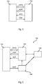
Figure 1 shows a typical electronic system comprising a plurality of processing systems; -
Figure 2 shows an exemplary processing system comprising at least one memory and a processing unit; -
Figure 3 shows an embodiment of the communication channel between a memory and a processing unit; -
Figure 4 shows an embodiment of a memory comprising an error detection and/or correction circuit; -
Figure 5 shows an embodiment of a processing system comprising a processing unit, a memory and an error handling circuit; -
Figure 6 shows an embodiment of the error handling circuit ofFigure 5 ; -
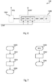
Figure 7 is a flowchart showing an embodiment of the operation of the processing unit ofFigure 5 ; -
Figures 8 and 9 show a second embodiment of an error handling circuit; -
Figure 10 shows a third embodiment of an error handling circuit; and -
Figure 11 shows an embodiment of an electronic system comprising a plurality of processing systems and a fault collection unit. - In the following description, numerous specific details are given to provide a thorough understanding of embodiments. The embodiments can be practiced without one or several specific details, or with other methods, components, materials, etc. In other instances, well-known structures, materials, or operations are not shown or described in detail to avoid obscuring aspects of the embodiments.
- Reference throughout this specification to "one embodiment" or "an embodiment" means that a particular feature, structure, or characteristic described in connection with the embodiment is included in at least one embodiment. Thus, the appearances of the phrases "in one embodiment" or "in an embodiment" in various places throughout this specification are not necessarily all referring to the same embodiment. Furthermore, the particular features, structures, or characteristics may be combined in any suitable manner in one or more embodiments.
- The headings provided herein are for convenience only and do not interpret the scope or meaning of the embodiments.
- In the following
Figures 3 to 11 parts, elements or components which have already been described with reference toFigures 1 and 2 are denoted by the same references previously used in such Figures; the description of such previously described elements will not be repeated in the following in order not to overburden the present detailed description. - As mentioned before, various embodiments of the present disclosure relate to solutions for managing errors in the data read from a
memory 104. -
Figure 3 shows again aprocessing system 10 comprising aprocessing unit 102 and amemory 104, such as anon-volatile memory 104a or avolatile memory 104b. Accordingly the description ofFigure 2 fully applies also to the system ofFigure 3 . - In the embodiment considered, the
processing unit 102 is connected via a suitable communication channel to thememory 104 in order to provide an address signal ADR to thememory 104 and receive respective data DATA from thememory 104. In case of programmable memories 104 (such asvolatile memories 104b or programmablenon-volatile memories 104a), theprocessing unit 102 may also be configured to transmit respective data DATA for a given address ADR to thememory 104. Usually, for this purpose theprocessing unit 102 provides one or more control signals to thememory 104 in order to select the operation to be performed, such as a write/read control signal W/R used to select a write or read operation to be performed for a given address ADR. - Generally, the communication channel for transmitting the address signal ADR and the data signal DATA may be any suitable communication channel, including serial or parallel communication channels, bi-direction or plural unidirectional communication channels, synchronous or asynchronous communication channels. For example, in various embodiments the
memory 104 comprises a first number NADR (e.g. 8, 16, 32, 64 bits) of input terminals for receiving the address signal ADR and a second number NDATA (e.g. 8, 16, 32, 64 bits) of input/output terminals for exchanging the data signal DATA. Accordingly, the first number NADR defines the address space of thememory 104 and the second number NDATA corresponds to the length of the data exchanged with thememory 104. - In various embodiments, the
memory 104 may also support an error detection and/or error correction function in order to detect and/or correct errors in the data read from thememory 104. In this case, thememory 104 may also provide one or more error signal ERR to theprocessing unit 102 indicating e.g. that the data contain an error and/or that an error in the data has been corrected or not. - For example,
Figure 4 shows a possible embodiment of amemory 104, such as a semiconductor memory, configured to detect and possibly correct errors in the data read from the memory. Such a memory is known e.g. from documentUS 5,233,616 . - Specifically, in the embodiment considered, the
memory 104 comprises amemory area 200 comprising one or more memory cells. For example, the memory cells may be arranged in a plurality of rows and optionally columns. For example, each memory cell may be a RAM or flash cell. - As mentioned before, the
memory 104 receives at input the address signal ADR, wherein the address signal ADR is used to select a given sub-area within thememory area 200. For example, the address signal ADR may be provided to arow decoder 202 and anoptional column decoder 204 in order to select a given sub-area in thememory area 200, i.e. a given number of bits NMEM within thememory area 200. In various embodiments, the address signal ADR may not be provided directly to the row (and column) decoder, but the address signal ADR may be stored in anaddress buffer 208. - As mentioned before, the
memory 104 also comprises one or more input and/or output terminals for exchanging the data signal DATA. Generally, also the data signal DATA may be stored in adata buffer 218. - For example, in the embodiment considered, the
memory 104 supports both read and write operations, which may be selected via a control signal W/R. Specifically, in the embodiment considered, thememory area 200 has associated a write and readinterface 206. For example, the interface may comprise a write driver in order to write data to the selected memory sub-area and a sense amplifier in order to read data from the selected memory sub-area. - In a conventional memory, the write and read
interface 206 would operate directly with the data exchanged via the data signal DATA, e.g. when using a bi-directional data bus, the memory provides the data read from the selected memory sub-area having NMEM = NDATA bits via the signal DATA or the memory stores the NMEM = NDATA bits received via the signal DATA to the selected memory sub-area. - Conversely, in a
memory 104 supporting an error detection and/or correction function, the number of bits NMEM of the selected memory sub-area is greater than the number of bits NDATA of the data signal DATA. For example, as schematically shown inFigure 4 , each sub-area of thememory area 200 may consist in a first field DA having the number of bits NDATA for storing data DATA and a second field PA having NPA bits for storing one or more additional bits, with NMEM = NDATA + NPA . - In this case the
memory 104 may comprises anerror processing circuit 210 which manages the data exchange between the data signal DATA and theinterface 206. Specifically, theerror processing circuit 210 comprises at least anencoder module 216 and adecoder module 214. - Specifically, when performing a write operation (as selected e.g. via the signal W/R), the
encoder module 216 is configured to encode the data signal DATA (having NDATA bits) in order to generate encoded data (having NMEM bits) and provide the encoded data to theinterface 206 in order to write the encoded data to the selected memory sub-area. For example, theencoder module 216 may calculate the error correction bits PA to be stored with the data. - Conversely, when performing a read operation (as selected e.g. via the signal W/R), the
decoder module 214 is configured to decode the data of the selected memory sub-area (having NMEM bits) in order to generate decoded data (having NDATA bits) and provide the decoded data via the data signal DATA. For example, when using additional error detection bits (e.g. parity bits) PA, the decoded data may directly correspond to the field DA. However, thedecoder module 214 also processes the additional bits in order to determine whether the data read from thememory area 200 contain valid data, e.g. by using the error detection bits PA. For example, in the embodiment considered, thedecoder module 214 may recalculate the error detection bits for the data DA read and compare the calculated error detection bits with the bits of the field PA read from the memory. In this case, thedecoder module 214 may thus generate an error signal ERR when the error detection data do not correspond. Usually, the number of error detection bits PA is correlated to the number of errors which may be detected in the data field DA. - Generally, also more complex encoding/decoding schemes may be used, e.g. in order to support not only error detection but also error correction. An overview of the difference between error detection and error correction codes may be found at "https://en.wikipedia.org/wiki/ Error_detection_and_correction/".
- For example, when using encoding/decoding methods permitting also an error correction, the
error processing circuit 210 comprises also anerror correction circuit 212, which may also be combined directly with thedecoder module 214. Specifically, theerror correction circuit 212 is configured to reconstruct the original data written to the memory are 200 even in case of one or more errors (based on the encoding scheme used) in the data read from the selected memory sub-area, such as in the data field DA and/or the field PA. - The operation of such a
memory 104 is well known in the art, e.g. in the contexts of Error-Correcting Code (ECC) memories. - In various embodiments, the
error correction circuit 212 may thus generate an error signal ERR when theerror correction circuit 212 is unable to correct the error in the data read from the memory. - Accordingly, in various embodiments, the error signal ERR provided by the
memory 104 may signal for each read operation an error code indicating that the data read from the memory 104: - 1) do not contain error,
- 2) contain at least one error, but the error could be corrected; possibly also indicating the number of bits which contained errors (e.g. by using different error codes), or
- 3) contain at least one error and the error could not be corrected.
- Thus, based on the error code of the error signal ERR, the
processing system 10a may perform different operations. - For example,
Figure 5 shows an embodiment of aprocessing system 10a, wherein theprocessing unit 102 has associated anerror handling circuit 108. Specifically, in the embodiment considered, theerror handling circuit 108 receives at input the one or more error signals ERR provided by thememory 104. - For example,
Figure 6 shows a first embodiment of theerror handling circuit 108. - In the embodiment considered, the
error handling circuit 108 comprise aregister 1080 providing an error signal ERR'. Specifically, in various embodiments, theregister 1080 is addressable by theprocessing unit 102, so called special function register. For example, in the embodiment considered, thememory 104 supports an error correction code able to correct up to two-bit errors. In this case, the error signal ERR may comprise three bits: - a bit SBC indicating a single bit error having been corrected;
- a bit DBC indicating a double bit error having been corrected; and
- a bit UC indicating that the error was not corrected.
- For example, in case all bits are low ("000"), the error signal ERR indicates that no error occurred, while a single bit is set when a memory error is signaled.
- In various embodiments, the error signal ERR' has the same number of bits as the error signal ERR and the same encoding is used for the error codes, i.e. in the embodiment considered, the register comprises three error bits SBC, DBC and UC. Generally, also other encoding schemes may be used for the error codes/types and the encoding of the error signal ERR provided by the
memory 104 may be different from the encoding of the error signal ERR'. For example, the error signal ERR and/or the error signal ERR' may have two bits (e.g. "00" for no error, "01" for single bit error, "10" for double-bit error and "11" for uncorrected error). Accordingly, based on the encoding of the error codes of the error signal ERR, theerror handling circuit 108 generally sets the error bits in theregister 1080/error signal ERR' as a function of the error signal ERR. - In various embodiments, the
error handling circuit 108 may also comprise acircuit 1082 configured to manage the internal reactions of theprocessing system 10a. For example, such reactions may include the generation of an (non-maskable and/or maskable/configurable) interrupt, a reset, the activation of a debug mode, etc. - For example, in the following will be described, without loss of generality, a
circuit 1082 configured to operate as an interruptgenerator circuit 1082 configured to generate one or more interrupts IRQ as a function of the error signal ERR' (or directly the error signal ERR'). For example, in various embodiments the interruptgenerator circuit 1082 is configured to generate an interrupt signal IRQ when: - 1) one of the bits of the error signal ERR or ERR' is set;
- 2) the bit DBC is set or the bit UC is set; or
- 3) only the bit UC is set.
- In various embodiments, the mode of operation of the interrupt
generator circuit 1082 may be programable, e.g. by setting one or more interrupt enable bits in theregister 1080. For example, in various embodiments, theregister 1080 comprises for each error code indicating an error a respective error enable flag. For example, in the embodiment considered, theregister 1080 comprises three additional bits SBE, DBE and UE, which permit to specify whether the interruptgenerator circuit 1082 should set the interrupt IRQ when the respective bit SBC, DEC and UC is set. - In various embodiments, the error signal ERR' and the optional interrupt IRQ are provided to the
processing unit 102. - For example,
Figure 7 shows an embodiment of the operation of theprocessing unit 102, which e.g. may be implemented by a suitable programming of a micro-processor via software code. - After a
start step 2000, theprocessing unit 102 may enable at astep 2002 the generation of an interrupt for one or more error codes, e.g. by setting the bits SBE, DBE and UE in theregister 1080, thereby selecting the desired error detection behavior. Generally, thestep 2002 is purely option, because theprocessing unit 102 may also not re-program the respective default/reset values or the behavior of the interruptgenerator circuit 1082 may be fixed. - Next the processing unit may proceed to the
normal operation mode 2004, i.e. execute the application, which may include one or more read (and possibly also write) accesses to thememory 104, and the procedure ends at astop step 2006. - Once a read error is detected by the memory (see also
Figure 4 ), thememory 104 signals the respective error code via the error signal ERR and the interruptgenerator circuit 1082 generates an interrupt IRQ when the error code corresponds to enabled error code. - In response to the generation of an interrupt IRQ at a
step 2050, theprocessing unit 102 will thus start at astep 2052 an error handling routine, and once having executed the error handling routine theprocessing unit 102 returns to the normal operation at a stop step 2054 terminating the interrupt routine. For example, theprocessing unit 102 may read the content of theregister 1080, in particular the signal ERR', at thestep 2052 and select a given operation based on the type of error. For example, theprocessing unit 102 may not perform any operation when a single bit error is indicated. Conversely, the processing unit may monitor the number of double bit errors and provide an error message to a user when a given threshold is exceeded. Finally, theprocessing unit 102 may provide immediately the error message when an uncorrectable error has been detected. - For example, the method show in
Figure 7 may be useful in order to monitor errors in the RAM and/or non-volatile memory (e.g. Flash, PCM, etc.) of a micro-controller. For example, in this case eachmemory 104 may provide the respective error signal ERR to a respectiveerror handling circuit 108. In this way the error behavior for eachmemory 104 may also be configured independently, e.g. by setting the respective enable flags in therespective memory 1080. Generally, such pluralerror handling circuit 108 may also be combined in a singleerror handling circuit 108, e.g. by providing respective error bits and possibly error code enable flags in thememory 1080. - Moreover, the capabilities of the
memories non-volatile memory 104a may implement an error correction mechanism able to correct up to double-bit errors, while thevolatile memory 104b may only be able to correct single bit errors. - In addition or as alternative to sending the signal ERR' and/or the interrupt IRQ to the
processing unit 102, theinternal reaction circuit 1082 and theregister 1080 may also send one or more of these signals to anotherblock 106 of the processing unit, such as a communication interface, a reset circuit and/or a debug circuit. For example, the reset circuit may be configured to restart the processing system in a degraded mode when an uncorrectable error was detected (e.g. UC = "1"). Similarly, the signal ERR' and/or the interrupt IRQ may be provided to one or more pins of theprocessing system 10a. - Accordingly, the solution described with respect to
Figures 5 to 7 permits to selectively choose the behavior of theprocessing system 10a as a function of the type of a memory read error. - However, when integrating different applications within the
processing system 10a, only a single memory fault behavior may be configured for eachmemory 104. However, for certain applications it might be useful that a first type of applications, such as safety-critical applications, react in a different way than a second type of applications, such as non-safety critical application. For example, in various applications it may be useful that the second type of applications is only interrupted when the memory read error was not corrected, while the first type of application should already intervene when a single (or double) bit error has been detected. - For example, in the embodiment shown in
Figures 7 , theprocessing unit 102 could enable atstep 2002 the interrupt IRQ for any error type. In response to an error, theprocessing unit 102 may then determine at theerror handling step 2052 the currently executed application in order to decide how to treat the error, eventually ignoring also the error. However, in case of micro-processors each memory error would thus generate an interrupt, which thus causes an interruption of the execution of the application. - Accordingly, in the following will be described an embodiment, which further improves the treatment of memory errors directly at a hardware level.
- Specifically, in various embodiment, the
processing system 10a is configured to generate different triggers not only based on the error type (e.g. single-bit correctable fault SBC = "1", double-bit correctable fault DBC = "1", or non-correctable fault UC = "1"), but also based on the memory address ADR where the error occurred. - Specifically,
Figure 8 shows an embodiment of anerror handling circuit 108, which comprises an error collector and an optional internal reaction circuit 108' (essentially corresponding to thecircuit 108 described in the foregoing) and twoadditional logic circuits - Specifically, the
first circuit 1084 comprises a plurality of sub-blocks 10841...1084n wherein each block 1084i (with i = 1..n) is configured to determine whether the current address ADR belongs to a given memory address region, i.e. whether the current address ADR is between a respective lower limit RLi and upper limit RHi . For example, in the embodiment considered, eachbock 1084i comprises for this reason: - a first
digital comparator 1088i configured to determine whether the address ADR is greater than the respective lower limit RLi , - a second
digital comparator 1090i configured to determine whether the address ADR is smaller than the respective upper limit RHi , and - a
logic gate 1092i, such as an AND gate, combining the output signals of thecomparators - Accordingly, in the embodiment considered, each
block 1084i sets a respective enable signal TEi (corresponding e.g. to the output of the respective logic gate 1092i) when the address ADR belongs to a given memory address region. - In various embodiments, the limits RLi and RHi are programable. For example, the limits may be stored in special function registers of the
processing unit 102, e.g. in theregister 1080, or may be set by programing a given area in thenon-volatile program memory 104a of theprocessing unit 102. - The
second circuit 1086 receives at input the error signal ERR from thememory 104 and the enable signals TEi from theblock 1084. Specifically, thecircuit 1086 generates then a plurality of error signals ERR1 ..ERRn by combining the error signal ERR with the respective enable signal TEi . - Accordingly, only the error signals ERR1 ..ERRn will be set to the value of the current error signal ERR for which also the respective enable signal TEi is set. For example, considering the exemplary case where the error signal ERR comprises the bits SBC, DBC and UC, also each error signal ERRi comprises bits SBCi , DBCi and UCi . For example, assuming that the signals are set when the logic level is high, each bit of the signal ERRi may be obtained via a logic AND operation (e.g. at a logic gate 1094), i.e.:
SBCi = SBC AND TEi , DBCi = DBC AND TEi , UCi = UC AND TEi . - Accordingly, generally the
blocks circuit 1084 is configured to monitor the failed address ADR and, if it falls within any of the programmed memory windows, then it actives a respective enabling signal TEi in order to enable the respective error signal ERRi . - In various embodiments, the error signals ERR1 ..ERRn may thus again be provided to an error collector and optional internal reaction circuit 108'.
- For example
Figure 9 shows a possible embodiment of a circuit 108' configured to handle a plurality of error signals ERR1..ERRn. For example, such a circuit 108' could also be used to handle plural error signals generated by plural memories. - Specifically, similar to the description of
Figure 6 , theerror handling circuit 108 comprises aregister 1080, such as a special function register of theprocessing unit 102, for storing the error signals ERR1 ..ERRn . - For example, as shown in
Figure 9 , theregister 1080 may comprise a plurality of sub-register 10801..1080n, wherein each sub-register 1080i comprises a number of error bits for storing a respective error signal ERRi . For example, in the exemplary embodiment, each sub-register 1080i comprises three bits SECi , DBCi and UCi for storing the respective bits of the respective error signal ERRi . Thus generally, theregister 1080 generates a plurality of error signals ERR'1 ..ERR' n by storing the signals ERR1 ..ERRn . Again, each error signal ERR' may have also a different number of error bits and/or encoding scheme than the error signal ERR. - In various embodiments, the circuit 108' may also comprise an internal reaction circuit 1082 (such as an interrupt generator circuit) configured to generate one or more signals (such as an interrupt signal IRQ, a reset signal, etc.) as a function of the data stored in the sub-register 1080i. Similar to the description of
Figure 6 , each sub-register 1080i may thus also comprise one or more enable flags each enabling the generation an interrupt, a reset, etc. for a respective error code. For example, in the embodiment considered, each sub-register 1080i comprises three further bits SBEi , DBEi and UEi for enabling the generation of the interrupt IRQ when the respective bit SECi , DBCi and UCi is set. For example, in the embodiment considered, the interruptgenerator circuit 1082 may generate an interrupt when both a given error bit SBCi , DBCi or UCi and the respective enable flag SBEi , DBEi or UEi is set. -
Figure 10 shows a further embodiment of theerror handler circuit 108. - Specifically, instead of operating on the error signal ERR and storing the signals ERRi to the register 1080 (as described with respect to Figured 8 and 9),
Figure 10 shows an embodiment, wherein thecombinational circuit 1086 operates already on the error signal ERR' stored in theregister 1080 described with respect toFigure 6 . Specifically, in this case, thecircuit 1086 described with respect toFigure 8 receives at input the signal ERR' (and not the signal ERR). - In the embodiment considered, the output of the
circuit 1086 providing error signals ERR' 1 ..ERR' n may thus be connected directly to the optionalinternal reaction circuit 1082. In this case, theregister 1080 may still comprise the enable flag SBEi , DBEi or UEi for the different error codes, which are then used by theinternal reaction circuit 1082. In fact, generally, theblocks error processing circuit 210 of thememory 104 and the final module used to process the error signals ERR'1 ..ERR'n . - For example, also in this case the error signals ERR'1 ..ERR'n and/or the interrupt signal (s) IRQ may be provided to the
processing unit 102, anotherblock 106 of theprocessing system 10a and/or a pin of theprocessing system 10a. For example,Figure 11 shows an embodiment, wherein a plurality ofprocessing systems 10a, such as twoprocessing systems communication system 20. Generally, the architecture corresponds essentially to the architecture described with respect toFigure 1 and the respective description applies also in this case. For example, theprocessing systems 10a1 may be an engine control unit and theprocessing systems 10a2 may be a transmission control unit. - However, in the embodiment considered, the system comprises a further processing system FCCU connected to the
common system 20. Specifically, the processing system FCCU is configured to implement a fault collection control unit. Accordingly, in this case, eachprocessing system 10a may be configured to send the error signals ERR'1 ..ERR'n also to the processing system FCCU. Generally, the transmission may be managed via theprocessing unit 102 of the processing system, or theerror handling circuit 108 may provide directly the error signals ERR'1 ..ERR'n and possibly the interrupt signal IRQ to acommunication interface 106 of theprocessing system 10a (connected to the communication channel 10), which thus may transmit the error signals ERR'1 ..ERR'n to the system FCCU without the intervention of theprocessing unit 102. - Accordingly, the solutions described permit that the
memory 104 may be organized in different memory regions, such as a first (e.g. safety-critical) region identified by means of a first lower and upper address/limit RL1 /RH1 and a second (e.g. non-safety critical) region identified by means of a second lower and upper address/limit RL2/RH2. - In the embodiment considered, the
circuits Figure 10 ), wherein the first error signal ERR1 is set to the currently provided error signal ERR (or ERR' in the embodiment shown inFigure 10 ), when the address ADR belongs to the first range and the second error signal ERR2 is set to the currently provided error signal ERR (or ERR') when the address ADR belongs to the second range. - Accordingly, generally, the
processing unit 10a is configured to generate a plurality of error signals ERR'1 and ERR'2 based on the address ADR and these error signals ERR'1 and ERR'2 may be processed separately, thereby permitting a faster reaction time. For example, the interruptgenerator circuit 1082 may be used to selectively generate an interrupt IRQ (or any other kind of trigger signal used to activate a given operation in response to a memory read error for a given memory range). For example, the interrupthandler 1082 may be configured via the respective enable flags (e.g. stored in the register 1080) to: - active the interrupt IRQ already for a single bit error when the address belongs to the first region (e.g., SBE1 = "1", DBE1 = "1", UE1 = "1"), and
- active the interrupt IRQ only for an uncorrectable error when the address belongs to the second region (e.g., SBE2 = "0", DBE2 = "0", UE2 = "1").
- Of course, without prejudice to the principle of the invention, the details of construction and the embodiments may vary widely with respect to what has been described and illustrated herein purely by way of example, without thereby departing from the scope of the present invention, as defined by the ensuing claims.
Claims (13)
- A processing system (10a) comprising:- a processing unit (102) arranged to be connected to a memory with error detection and/or correction (104), said processing unit (102) configured to generate at least one read request for reading data (DATA) from said memory with error detection and/or correction (104), said read request comprising an address signal (ADR) identifying the address of a given memory area in said memory (104);- an error handling circuit (108) arranged to be connected to said memory with error detection and/or correction (104) for receiving an error signal (ERR) from said memory with error detection and/or correction (104), wherein said error signal (ERR) contains an error code indicating whether the data (DATA) read from said memory with error detection and/or correction (104) do contain errors (UC);wherein said error handling circuit (108) is configured to generate a first error signal (ERR'1 ) and a second error signal (ERR'n ), wherein said error handling circuit (108) comprises a hardware circuit (1084, 1086) configured to:- determine whether the address indicated by said address signal (ADR) belongs to a first address range (RL1, RH1 );- set said first error signal (ERR'1 ) to the error code of said error signal (ERR) when the address indicated by said address signal (ADR) belongs to said first address range (RL 1,RH 1);- determine whether the address indicated by said address signal (ADR) belongs to a second address range (RLn,RHn ); and- set said second error signal (ERR'n ) to the error code of said error signal (ERR) when the address indicated by said address signal (ADR) belongs to said second address range (RLn ,RHn ).
- The processing system (10a) according to Claim 1, wherein said hardware circuit (1084, 1086) comprises:- a first combinational logic circuit (10841) configured to set a first enable signal (TE1 ) to:- a first logic value when the address indicated by said address signal (ADR) belongs to said first address range (RL 1,RH1 ), and- a second logic value when the address indicated by said address signal (ADR) does not belong to said first address range (RL1 ,RH1 );- a second combinational logic circuit (1084n) configured to set a second enable signal (TEn ) to:- a first logic value when the address indicated by said address signal (ADR) belongs to said second address range (RLn ,RHn ), and- a second logic value when the address indicated by said address signal (ADR) does not belong to said second address range (RLn ,RHn ); and- a third combinational logic circuit (1086) configured to:- set said first error signal (ERR'1 ) to the error code of said error signal (ERR) when said first enable signal (TE1 ) has said first logic value, and- set said second error signal (ERR'n ) to the error code of said error signal (ERR) when said second enable signal (TEn ) has said first logic value.
- The processing system (10a) according to Claim 1 or Claim 2, wherein said first address range (RL1 ,RH1 ) and/or said second address range (RLn,RHn ) are programmable.
- The processing system (10a) according to any of the previous claims, wherein said error handling circuit (108) comprises:- a register (1080) configured to store the error code of said error signal (ERR) and provide the stored error code (ERR') to said hardware circuit (1084, 1086) for generating said first error signal (ERR'1 ) and said second error signal (ERR'n ); and/or- a register (1080) configured to store the error code of said first error signal (ERR'1 ) and the error code of said second error signal (ERR'n ).
- The processing system (10a) according to any of the previous claims, comprising an interrupt generator circuit (1082) configured to generate one or more interrupt signals (IRQ) when the error code of said first error signal (ERR'1 ) corresponds to one or more first reference values (SBE1 , DBE1 , UE1 ) and/or the error code of said second error signal (ERR'n ) corresponds to one or more second reference values (SBEn, DBEn , UEn ).
- The processing system (10a) according to Claim 5, wherein said one or more first reference values (SBE1 , DBE1, UE1 ) and/or said one or more second reference values (SBEn, DBEn , UEn ) are programmable (1080).
- The processing system (10a) according to Claim 5 or Claim 6, wherein:- at least one of said one or more interrupt signals (IRQ), said first error signal (ERR'1 ) and said second error signal (ERR'n ) are provided to said processing unit (102); and/or- said processing system (10a) comprises a communication interface (106), and wherein at least one of said one or more interrupt signals (IRQ), said first error signal (ERR'1 ) and said second error signal (ERR'n ) are provided directly to said communication interface (106); and/or- said processing system (10a) comprises a pin, and wherein at least one of said one or more interrupt signals (IRQ), said first error signal (ERR'1 ) and said second error signal (ERR'n ) are provided directly to said pin.
- The processing system (10a) according to any of the previous claims, wherein said error signal (ERR) comprises a plurality of bits (SBC, DBC, UC), and wherein the error code of said error signal (ERR) indicates at least:- no error occurred during the reading operation of said data (DATA);- an error occurred during the reading operation of said data (DATA), but the error was corrected; and- an error occurred during the reading operation of said data (DATA) and the error was not corrected.
- The processing system (10a) according to any of the previous claims, wherein said processing unit (102) is a micro-processor adapted to be programmed via software instructions.
- The processing system (10a) according to any of the previous claims, comprising said memory with error detection and/or correction (104).
- The processing system (10a) according to Claim 10, wherein said memory with error detection and/or correction (104) includes at least one of a non-volatile memory (104a) arranged to store the firmware for said processing unit (102) and a Random-Access Memory (104b) arranged to store temporary results of the processing of said processing unit (102).
- An integrated circuit, such as a micro-controller, comprising a processing system (10a) according to any of Claims 1 to 11.
- A method of operating a processing system (10a) according to any of Claim 1 to 11, comprising the steps of:- storing data into said memory with error detection and/or correction (104);- generate via said processing unit (102) at least one read request for reading data (DATA) from a given address (ADR) of said memory with error detection and/or correction (104); and- generating via said error handling circuit (108) said first error signal (ERR'1 ) and said second error signal (ERR'n ) as a function of said given address (ADR) and said error signal (ERR) received from said memory with error detection and/or correction (104).
Applications Claiming Priority (1)
| Application Number | Priority Date | Filing Date | Title |
|---|---|---|---|
| IT102018000003233A IT201800003233A1 (en) | 2018-03-02 | 2018-03-02 | PROCESSING SYSTEM, RELATED INTEGRATED CIRCUIT AND PROCEDURE |
Publications (2)
| Publication Number | Publication Date |
|---|---|
| EP3534262A1 true EP3534262A1 (en) | 2019-09-04 |
| EP3534262B1 EP3534262B1 (en) | 2020-11-04 |
Family
ID=62143522
Family Applications (1)
| Application Number | Title | Priority Date | Filing Date |
|---|---|---|---|
| EP19159273.2A Active EP3534262B1 (en) | 2018-03-02 | 2019-02-26 | Processing system, related integrated circuit and method |
Country Status (3)
| Country | Link |
|---|---|
| US (1) | US11068331B2 (en) |
| EP (1) | EP3534262B1 (en) |
| IT (1) | IT201800003233A1 (en) |
Cited By (2)
| Publication number | Priority date | Publication date | Assignee | Title |
|---|---|---|---|---|
| EP4120083A1 (en) * | 2021-07-13 | 2023-01-18 | STMicroelectronics Application GmbH | Processing system, related integrated circuit, device and method |
| IT202200006455A1 (en) | 2022-04-01 | 2023-10-01 | Stmicroelectronics Application Gmbh | Processing system, related integrated circuit, device and process |
Families Citing this family (7)
| Publication number | Priority date | Publication date | Assignee | Title |
|---|---|---|---|---|
| CN115145753A (en) * | 2021-03-30 | 2022-10-04 | 意法半导体应用有限公司 | Processing system, related integrated circuit, apparatus and method |
| US12530260B2 (en) * | 2021-11-14 | 2026-01-20 | Sk Hynix Nand Product Solutions Corp. | Circuits and methods for correcting errors in memory |
| CN114333968B (en) * | 2021-12-29 | 2025-01-24 | 北京奕斯伟计算技术股份有限公司 | Memory control method, memory controller and electronic device |
| CN116701045A (en) * | 2022-03-03 | 2023-09-05 | 意法半导体股份有限公司 | Processing systems, related integrated circuits, devices and methods |
| US12130700B2 (en) * | 2023-03-02 | 2024-10-29 | Hamilton Sundstrand Corporation | RAM test with parity error detection and handling |
| FR3158375B1 (en) * | 2024-01-11 | 2025-12-12 | St Microelectronics Int Nv | INTERRUPTION MANAGEMENT OF AN INTEGRATED CIRCUIT MEMORY CONTROLLER |
| US12385975B1 (en) * | 2024-02-13 | 2025-08-12 | Ampere Computing Llc | Integrated circuits including error protection of fields in transferred information and field-based error signals and related methods |
Citations (2)
| Publication number | Priority date | Publication date | Assignee | Title |
|---|---|---|---|---|
| US20100064205A1 (en) * | 2008-09-05 | 2010-03-11 | Moyer William C | Selective cache way mirroring |
| US20110047408A1 (en) * | 2009-08-20 | 2011-02-24 | Arm Limited | Handling of hard errors in a cache of a data processing apparatus |
Family Cites Families (11)
| Publication number | Priority date | Publication date | Assignee | Title |
|---|---|---|---|---|
| US6453429B1 (en) * | 1999-04-29 | 2002-09-17 | International Business Machines Corporation | Method and apparatus for bus hang detection and identification of errant agent for fail safe access to trapped error information |
| US7725803B1 (en) * | 2006-11-08 | 2010-05-25 | Lattice Semiconductor Corporation | Programmable logic device programming verification systems and methods |
| TW200849002A (en) * | 2007-06-01 | 2008-12-16 | Holtek Semiconductor Inc | Control device and control method |
| JP2009043321A (en) * | 2007-08-08 | 2009-02-26 | Toshiba Corp | Optical disk playback device |
| US8762797B2 (en) * | 2011-04-29 | 2014-06-24 | Google Inc. | Method and apparatus for detecting memory access faults |
| US9202591B2 (en) * | 2013-05-10 | 2015-12-01 | Omnivision Technologies, Inc. | On-line memory testing systems and methods |
| US9495239B1 (en) * | 2014-08-22 | 2016-11-15 | Xilinx, Inc. | User-configurable error handling |
| US9583219B2 (en) * | 2014-09-27 | 2017-02-28 | Qualcomm Incorporated | Method and apparatus for in-system repair of memory in burst refresh |
| JP6455168B2 (en) * | 2015-01-16 | 2019-01-23 | 株式会社デンソー | Memory device system |
| JP2016167669A (en) * | 2015-03-09 | 2016-09-15 | 富士通株式会社 | Programmable logic circuit device and error detection method |
| US9916217B2 (en) * | 2016-01-05 | 2018-03-13 | Lenovo Enterprise Solutions (Singapore) Pte. Ltd. | Accessing hidden diagnostic registers |
-
2018
- 2018-03-02 IT IT102018000003233A patent/IT201800003233A1/en unknown
-
2019
- 2019-02-26 EP EP19159273.2A patent/EP3534262B1/en active Active
- 2019-02-28 US US16/289,425 patent/US11068331B2/en active Active
Patent Citations (2)
| Publication number | Priority date | Publication date | Assignee | Title |
|---|---|---|---|---|
| US20100064205A1 (en) * | 2008-09-05 | 2010-03-11 | Moyer William C | Selective cache way mirroring |
| US20110047408A1 (en) * | 2009-08-20 | 2011-02-24 | Arm Limited | Handling of hard errors in a cache of a data processing apparatus |
Cited By (5)
| Publication number | Priority date | Publication date | Assignee | Title |
|---|---|---|---|---|
| EP4120083A1 (en) * | 2021-07-13 | 2023-01-18 | STMicroelectronics Application GmbH | Processing system, related integrated circuit, device and method |
| US11764807B2 (en) | 2021-07-13 | 2023-09-19 | Stmicroelectronics Application Gmbh | Processing system, related integrated circuit, device and method |
| IT202200006455A1 (en) | 2022-04-01 | 2023-10-01 | Stmicroelectronics Application Gmbh | Processing system, related integrated circuit, device and process |
| EP4254196A1 (en) | 2022-04-01 | 2023-10-04 | STMicroelectronics Application GmbH | Processing system, related integrated circuit, device and method |
| US12019118B2 (en) | 2022-04-01 | 2024-06-25 | Stmicroelectronics International N.V. | Processing system, related integrated circuit, device and method |
Also Published As
| Publication number | Publication date |
|---|---|
| IT201800003233A1 (en) | 2019-09-02 |
| US20190272211A1 (en) | 2019-09-05 |
| US11068331B2 (en) | 2021-07-20 |
| EP3534262B1 (en) | 2020-11-04 |
Similar Documents
| Publication | Publication Date | Title |
|---|---|---|
| EP3534262B1 (en) | Processing system, related integrated circuit and method | |
| US11977438B2 (en) | Processing system, related integrated circuit and method | |
| KR100842680B1 (en) | Error Correction Controller of Flash Memory Device and Memory System Including It | |
| US11726665B1 (en) | Memory extension with error correction | |
| US20150220387A1 (en) | Error correction in non_volatile memory | |
| KR102766655B1 (en) | Memory device and electronic device performing adaptive error correction with pre-checking error rate and method of operating the memory device | |
| US20230027826A1 (en) | Processing system, related integrated circuit, device and method | |
| CN104765650A (en) | Data processing apparatus | |
| WO2005076133A1 (en) | An error detection and correction scheme for a memory device | |
| JP2008299855A (en) | MEMORY SYSTEM WITH MULTICHANNEL ERROR CORRECTION CODER USING EMBEDDED MEMORY AND METHOD THEREOF | |
| JP7157516B2 (en) | Error correction using hierarchical decoder | |
| US12210411B2 (en) | Host-based error correction | |
| CN106469099A (en) | Error correcting in the case of application WOM code | |
| EP4141677B1 (en) | Processing system, related integrated circuit, device and method | |
| KR20200038320A (en) | Code rate switching mechanism for flash memory | |
| US9286156B2 (en) | Data storage device and method for processing error correction code thereof | |
| CN112068985B (en) | NORFLASH memory ECC error detection and correction method and system with programming instruction recognition | |
| US11971775B2 (en) | Predicting an unsuccessful error correction code condition using a dynamic read threshold table | |
| JP4950214B2 (en) | Method for detecting a power outage in a data storage device and method for restoring a data storage device | |
| CN117056149B (en) | Memory testing method and device, computing equipment and storage medium | |
| US20250053478A1 (en) | Memory system | |
| TWI922241B (en) | Memory device with error correction code | |
| US7730357B2 (en) | Integrated memory system | |
| CN101366009A (en) | Data processing system with error correction and method of operation thereof | |
| TW202541037A (en) | Memory device with error correction code |
Legal Events
| Date | Code | Title | Description |
|---|---|---|---|
| PUAI | Public reference made under article 153(3) epc to a published international application that has entered the european phase |
Free format text: ORIGINAL CODE: 0009012 |
|
| STAA | Information on the status of an ep patent application or granted ep patent |
Free format text: STATUS: THE APPLICATION HAS BEEN PUBLISHED |
|
| AK | Designated contracting states |
Kind code of ref document: A1 Designated state(s): AL AT BE BG CH CY CZ DE DK EE ES FI FR GB GR HR HU IE IS IT LI LT LU LV MC MK MT NL NO PL PT RO RS SE SI SK SM TR |
|
| AX | Request for extension of the european patent |
Extension state: BA ME |
|
| STAA | Information on the status of an ep patent application or granted ep patent |
Free format text: STATUS: REQUEST FOR EXAMINATION WAS MADE |
|
| 17P | Request for examination filed |
Effective date: 20200302 |
|
| RBV | Designated contracting states (corrected) |
Designated state(s): AL AT BE BG CH CY CZ DE DK EE ES FI FR GB GR HR HU IE IS IT LI LT LU LV MC MK MT NL NO PL PT RO RS SE SI SK SM TR |
|
| GRAJ | Information related to disapproval of communication of intention to grant by the applicant or resumption of examination proceedings by the epo deleted |
Free format text: ORIGINAL CODE: EPIDOSDIGR1 |
|
| GRAP | Despatch of communication of intention to grant a patent |
Free format text: ORIGINAL CODE: EPIDOSNIGR1 |
|
| GRAP | Despatch of communication of intention to grant a patent |
Free format text: ORIGINAL CODE: EPIDOSNIGR1 |
|
| STAA | Information on the status of an ep patent application or granted ep patent |
Free format text: STATUS: GRANT OF PATENT IS INTENDED |
|
| INTG | Intention to grant announced |
Effective date: 20200616 |
|
| GRAS | Grant fee paid |
Free format text: ORIGINAL CODE: EPIDOSNIGR3 |
|
| GRAA | (expected) grant |
Free format text: ORIGINAL CODE: 0009210 |
|
| STAA | Information on the status of an ep patent application or granted ep patent |
Free format text: STATUS: THE PATENT HAS BEEN GRANTED |
|
| AK | Designated contracting states |
Kind code of ref document: B1 Designated state(s): AL AT BE BG CH CY CZ DE DK EE ES FI FR GB GR HR HU IE IS IT LI LT LU LV MC MK MT NL NO PL PT RO RS SE SI SK SM TR |
|
| REG | Reference to a national code |
Ref country code: GB Ref legal event code: FG4D |
|
| REG | Reference to a national code |
Ref country code: CH Ref legal event code: EP |
|
| REG | Reference to a national code |
Ref country code: AT Ref legal event code: REF Ref document number: 1331691 Country of ref document: AT Kind code of ref document: T Effective date: 20201115 |
|
| REG | Reference to a national code |
Ref country code: DE Ref legal event code: R096 Ref document number: 602019001136 Country of ref document: DE |
|
| REG | Reference to a national code |
Ref country code: IE Ref legal event code: FG4D |
|
| REG | Reference to a national code |
Ref country code: NL Ref legal event code: MP Effective date: 20201104 |
|
| REG | Reference to a national code |
Ref country code: AT Ref legal event code: MK05 Ref document number: 1331691 Country of ref document: AT Kind code of ref document: T Effective date: 20201104 |
|
| PG25 | Lapsed in a contracting state [announced via postgrant information from national office to epo] |
Ref country code: RS Free format text: LAPSE BECAUSE OF FAILURE TO SUBMIT A TRANSLATION OF THE DESCRIPTION OR TO PAY THE FEE WITHIN THE PRESCRIBED TIME-LIMIT Effective date: 20201104 Ref country code: PT Free format text: LAPSE BECAUSE OF FAILURE TO SUBMIT A TRANSLATION OF THE DESCRIPTION OR TO PAY THE FEE WITHIN THE PRESCRIBED TIME-LIMIT Effective date: 20210304 Ref country code: FI Free format text: LAPSE BECAUSE OF FAILURE TO SUBMIT A TRANSLATION OF THE DESCRIPTION OR TO PAY THE FEE WITHIN THE PRESCRIBED TIME-LIMIT Effective date: 20201104 Ref country code: GR Free format text: LAPSE BECAUSE OF FAILURE TO SUBMIT A TRANSLATION OF THE DESCRIPTION OR TO PAY THE FEE WITHIN THE PRESCRIBED TIME-LIMIT Effective date: 20210205 Ref country code: NO Free format text: LAPSE BECAUSE OF FAILURE TO SUBMIT A TRANSLATION OF THE DESCRIPTION OR TO PAY THE FEE WITHIN THE PRESCRIBED TIME-LIMIT Effective date: 20210204 |
|
| PG25 | Lapsed in a contracting state [announced via postgrant information from national office to epo] |
Ref country code: ES Free format text: LAPSE BECAUSE OF FAILURE TO SUBMIT A TRANSLATION OF THE DESCRIPTION OR TO PAY THE FEE WITHIN THE PRESCRIBED TIME-LIMIT Effective date: 20201104 Ref country code: AT Free format text: LAPSE BECAUSE OF FAILURE TO SUBMIT A TRANSLATION OF THE DESCRIPTION OR TO PAY THE FEE WITHIN THE PRESCRIBED TIME-LIMIT Effective date: 20201104 Ref country code: BG Free format text: LAPSE BECAUSE OF FAILURE TO SUBMIT A TRANSLATION OF THE DESCRIPTION OR TO PAY THE FEE WITHIN THE PRESCRIBED TIME-LIMIT Effective date: 20210204 Ref country code: SE Free format text: LAPSE BECAUSE OF FAILURE TO SUBMIT A TRANSLATION OF THE DESCRIPTION OR TO PAY THE FEE WITHIN THE PRESCRIBED TIME-LIMIT Effective date: 20201104 Ref country code: IS Free format text: LAPSE BECAUSE OF FAILURE TO SUBMIT A TRANSLATION OF THE DESCRIPTION OR TO PAY THE FEE WITHIN THE PRESCRIBED TIME-LIMIT Effective date: 20210304 Ref country code: PL Free format text: LAPSE BECAUSE OF FAILURE TO SUBMIT A TRANSLATION OF THE DESCRIPTION OR TO PAY THE FEE WITHIN THE PRESCRIBED TIME-LIMIT Effective date: 20201104 Ref country code: LV Free format text: LAPSE BECAUSE OF FAILURE TO SUBMIT A TRANSLATION OF THE DESCRIPTION OR TO PAY THE FEE WITHIN THE PRESCRIBED TIME-LIMIT Effective date: 20201104 |
|
| REG | Reference to a national code |
Ref country code: LT Ref legal event code: MG9D |
|
| PG25 | Lapsed in a contracting state [announced via postgrant information from national office to epo] |
Ref country code: HR Free format text: LAPSE BECAUSE OF FAILURE TO SUBMIT A TRANSLATION OF THE DESCRIPTION OR TO PAY THE FEE WITHIN THE PRESCRIBED TIME-LIMIT Effective date: 20201104 |
|
| PG25 | Lapsed in a contracting state [announced via postgrant information from national office to epo] |
Ref country code: EE Free format text: LAPSE BECAUSE OF FAILURE TO SUBMIT A TRANSLATION OF THE DESCRIPTION OR TO PAY THE FEE WITHIN THE PRESCRIBED TIME-LIMIT Effective date: 20201104 Ref country code: SM Free format text: LAPSE BECAUSE OF FAILURE TO SUBMIT A TRANSLATION OF THE DESCRIPTION OR TO PAY THE FEE WITHIN THE PRESCRIBED TIME-LIMIT Effective date: 20201104 Ref country code: SK Free format text: LAPSE BECAUSE OF FAILURE TO SUBMIT A TRANSLATION OF THE DESCRIPTION OR TO PAY THE FEE WITHIN THE PRESCRIBED TIME-LIMIT Effective date: 20201104 Ref country code: CZ Free format text: LAPSE BECAUSE OF FAILURE TO SUBMIT A TRANSLATION OF THE DESCRIPTION OR TO PAY THE FEE WITHIN THE PRESCRIBED TIME-LIMIT Effective date: 20201104 Ref country code: RO Free format text: LAPSE BECAUSE OF FAILURE TO SUBMIT A TRANSLATION OF THE DESCRIPTION OR TO PAY THE FEE WITHIN THE PRESCRIBED TIME-LIMIT Effective date: 20201104 Ref country code: LT Free format text: LAPSE BECAUSE OF FAILURE TO SUBMIT A TRANSLATION OF THE DESCRIPTION OR TO PAY THE FEE WITHIN THE PRESCRIBED TIME-LIMIT Effective date: 20201104 |
|
| REG | Reference to a national code |
Ref country code: DE Ref legal event code: R097 Ref document number: 602019001136 Country of ref document: DE |
|
| PG25 | Lapsed in a contracting state [announced via postgrant information from national office to epo] |
Ref country code: DK Free format text: LAPSE BECAUSE OF FAILURE TO SUBMIT A TRANSLATION OF THE DESCRIPTION OR TO PAY THE FEE WITHIN THE PRESCRIBED TIME-LIMIT Effective date: 20201104 |
|
| PLBE | No opposition filed within time limit |
Free format text: ORIGINAL CODE: 0009261 |
|
| STAA | Information on the status of an ep patent application or granted ep patent |
Free format text: STATUS: NO OPPOSITION FILED WITHIN TIME LIMIT |
|
| PG25 | Lapsed in a contracting state [announced via postgrant information from national office to epo] |
Ref country code: MC Free format text: LAPSE BECAUSE OF FAILURE TO SUBMIT A TRANSLATION OF THE DESCRIPTION OR TO PAY THE FEE WITHIN THE PRESCRIBED TIME-LIMIT Effective date: 20201104 |
|
| 26N | No opposition filed |
Effective date: 20210805 |
|
| REG | Reference to a national code |
Ref country code: BE Ref legal event code: MM Effective date: 20210228 |
|
| PG25 | Lapsed in a contracting state [announced via postgrant information from national office to epo] |
Ref country code: LU Free format text: LAPSE BECAUSE OF NON-PAYMENT OF DUE FEES Effective date: 20210226 Ref country code: IT Free format text: LAPSE BECAUSE OF FAILURE TO SUBMIT A TRANSLATION OF THE DESCRIPTION OR TO PAY THE FEE WITHIN THE PRESCRIBED TIME-LIMIT Effective date: 20201104 Ref country code: AL Free format text: LAPSE BECAUSE OF FAILURE TO SUBMIT A TRANSLATION OF THE DESCRIPTION OR TO PAY THE FEE WITHIN THE PRESCRIBED TIME-LIMIT Effective date: 20201104 Ref country code: NL Free format text: LAPSE BECAUSE OF FAILURE TO SUBMIT A TRANSLATION OF THE DESCRIPTION OR TO PAY THE FEE WITHIN THE PRESCRIBED TIME-LIMIT Effective date: 20201104 |
|
| PG25 | Lapsed in a contracting state [announced via postgrant information from national office to epo] |
Ref country code: SI Free format text: LAPSE BECAUSE OF FAILURE TO SUBMIT A TRANSLATION OF THE DESCRIPTION OR TO PAY THE FEE WITHIN THE PRESCRIBED TIME-LIMIT Effective date: 20201104 |
|
| PG25 | Lapsed in a contracting state [announced via postgrant information from national office to epo] |
Ref country code: FR Free format text: LAPSE BECAUSE OF NON-PAYMENT OF DUE FEES Effective date: 20210228 Ref country code: IE Free format text: LAPSE BECAUSE OF NON-PAYMENT OF DUE FEES Effective date: 20210226 |
|
| PG25 | Lapsed in a contracting state [announced via postgrant information from national office to epo] |
Ref country code: IS Free format text: LAPSE BECAUSE OF FAILURE TO SUBMIT A TRANSLATION OF THE DESCRIPTION OR TO PAY THE FEE WITHIN THE PRESCRIBED TIME-LIMIT Effective date: 20210304 |
|
| PG25 | Lapsed in a contracting state [announced via postgrant information from national office to epo] |
Ref country code: BE Free format text: LAPSE BECAUSE OF NON-PAYMENT OF DUE FEES Effective date: 20210228 |
|
| REG | Reference to a national code |
Ref country code: CH Ref legal event code: PL |
|
| REG | Reference to a national code |
Ref country code: DE Ref legal event code: R081 Ref document number: 602019001136 Country of ref document: DE Owner name: STMICROELECTRONICS INTERNATIONAL N.V., PLAN-LE, CH Free format text: FORMER OWNER: STMICROELECTRONICS APPLICATION GMBH, 85609 ASCHHEIM, DE |
|
| PG25 | Lapsed in a contracting state [announced via postgrant information from national office to epo] |
Ref country code: LI Free format text: LAPSE BECAUSE OF NON-PAYMENT OF DUE FEES Effective date: 20220228 Ref country code: CH Free format text: LAPSE BECAUSE OF NON-PAYMENT OF DUE FEES Effective date: 20220228 |
|
| PG25 | Lapsed in a contracting state [announced via postgrant information from national office to epo] |
Ref country code: CY Free format text: LAPSE BECAUSE OF FAILURE TO SUBMIT A TRANSLATION OF THE DESCRIPTION OR TO PAY THE FEE WITHIN THE PRESCRIBED TIME-LIMIT Effective date: 20201104 |
|
| PG25 | Lapsed in a contracting state [announced via postgrant information from national office to epo] |
Ref country code: HU Free format text: LAPSE BECAUSE OF FAILURE TO SUBMIT A TRANSLATION OF THE DESCRIPTION OR TO PAY THE FEE WITHIN THE PRESCRIBED TIME-LIMIT; INVALID AB INITIO Effective date: 20190226 |
|
| GBPC | Gb: european patent ceased through non-payment of renewal fee |
Effective date: 20230226 |
|
| PG25 | Lapsed in a contracting state [announced via postgrant information from national office to epo] |
Ref country code: GB Free format text: LAPSE BECAUSE OF NON-PAYMENT OF DUE FEES Effective date: 20230226 |
|
| PG25 | Lapsed in a contracting state [announced via postgrant information from national office to epo] |
Ref country code: GB Free format text: LAPSE BECAUSE OF NON-PAYMENT OF DUE FEES Effective date: 20230226 |
|
| PG25 | Lapsed in a contracting state [announced via postgrant information from national office to epo] |
Ref country code: MK Free format text: LAPSE BECAUSE OF FAILURE TO SUBMIT A TRANSLATION OF THE DESCRIPTION OR TO PAY THE FEE WITHIN THE PRESCRIBED TIME-LIMIT Effective date: 20201104 |
|
| PG25 | Lapsed in a contracting state [announced via postgrant information from national office to epo] |
Ref country code: TR Free format text: LAPSE BECAUSE OF FAILURE TO SUBMIT A TRANSLATION OF THE DESCRIPTION OR TO PAY THE FEE WITHIN THE PRESCRIBED TIME-LIMIT Effective date: 20201104 |
|
| PG25 | Lapsed in a contracting state [announced via postgrant information from national office to epo] |
Ref country code: MT Free format text: LAPSE BECAUSE OF FAILURE TO SUBMIT A TRANSLATION OF THE DESCRIPTION OR TO PAY THE FEE WITHIN THE PRESCRIBED TIME-LIMIT Effective date: 20201104 |
|
| PGFP | Annual fee paid to national office [announced via postgrant information from national office to epo] |
Ref country code: DE Payment date: 20260121 Year of fee payment: 8 |