EP3534221A1 - Optical element, laminate body, and book form - Google Patents
Optical element, laminate body, and book form Download PDFInfo
- Publication number
- EP3534221A1 EP3534221A1 EP17865768.0A EP17865768A EP3534221A1 EP 3534221 A1 EP3534221 A1 EP 3534221A1 EP 17865768 A EP17865768 A EP 17865768A EP 3534221 A1 EP3534221 A1 EP 3534221A1
- Authority
- EP
- European Patent Office
- Prior art keywords
- layer
- diffraction grating
- light
- optical element
- hologram
- Prior art date
- Legal status (The legal status is an assumption and is not a legal conclusion. Google has not performed a legal analysis and makes no representation as to the accuracy of the status listed.)
- Granted
Links
Images




Classifications
-
- B—PERFORMING OPERATIONS; TRANSPORTING
- B42—BOOKBINDING; ALBUMS; FILES; SPECIAL PRINTED MATTER
- B42D—BOOKS; BOOK COVERS; LOOSE LEAVES; PRINTED MATTER CHARACTERISED BY IDENTIFICATION OR SECURITY FEATURES; PRINTED MATTER OF SPECIAL FORMAT OR STYLE NOT OTHERWISE PROVIDED FOR; DEVICES FOR USE THEREWITH AND NOT OTHERWISE PROVIDED FOR; MOVABLE-STRIP WRITING OR READING APPARATUS
- B42D25/00—Information-bearing cards or sheet-like structures characterised by identification or security features; Manufacture thereof
- B42D25/30—Identification or security features, e.g. for preventing forgery
- B42D25/328—Diffraction gratings; Holograms
-
- B—PERFORMING OPERATIONS; TRANSPORTING
- B32—LAYERED PRODUCTS
- B32B—LAYERED PRODUCTS, i.e. PRODUCTS BUILT-UP OF STRATA OF FLAT OR NON-FLAT, e.g. CELLULAR OR HONEYCOMB, FORM
- B32B7/00—Layered products characterised by the relation between layers; Layered products characterised by the relative orientation of features between layers, or by the relative values of a measurable parameter between layers, i.e. products comprising layers having different physical, chemical or physicochemical properties; Layered products characterised by the interconnection of layers
- B32B7/02—Physical, chemical or physicochemical properties
-
- B—PERFORMING OPERATIONS; TRANSPORTING
- B42—BOOKBINDING; ALBUMS; FILES; SPECIAL PRINTED MATTER
- B42D—BOOKS; BOOK COVERS; LOOSE LEAVES; PRINTED MATTER CHARACTERISED BY IDENTIFICATION OR SECURITY FEATURES; PRINTED MATTER OF SPECIAL FORMAT OR STYLE NOT OTHERWISE PROVIDED FOR; DEVICES FOR USE THEREWITH AND NOT OTHERWISE PROVIDED FOR; MOVABLE-STRIP WRITING OR READING APPARATUS
- B42D25/00—Information-bearing cards or sheet-like structures characterised by identification or security features; Manufacture thereof
- B42D25/20—Information-bearing cards or sheet-like structures characterised by identification or security features; Manufacture thereof characterised by a particular use or purpose
- B42D25/23—Identity cards
-
- B—PERFORMING OPERATIONS; TRANSPORTING
- B42—BOOKBINDING; ALBUMS; FILES; SPECIAL PRINTED MATTER
- B42D—BOOKS; BOOK COVERS; LOOSE LEAVES; PRINTED MATTER CHARACTERISED BY IDENTIFICATION OR SECURITY FEATURES; PRINTED MATTER OF SPECIAL FORMAT OR STYLE NOT OTHERWISE PROVIDED FOR; DEVICES FOR USE THEREWITH AND NOT OTHERWISE PROVIDED FOR; MOVABLE-STRIP WRITING OR READING APPARATUS
- B42D25/00—Information-bearing cards or sheet-like structures characterised by identification or security features; Manufacture thereof
- B42D25/30—Identification or security features, e.g. for preventing forgery
- B42D25/324—Reliefs
-
- B—PERFORMING OPERATIONS; TRANSPORTING
- B42—BOOKBINDING; ALBUMS; FILES; SPECIAL PRINTED MATTER
- B42D—BOOKS; BOOK COVERS; LOOSE LEAVES; PRINTED MATTER CHARACTERISED BY IDENTIFICATION OR SECURITY FEATURES; PRINTED MATTER OF SPECIAL FORMAT OR STYLE NOT OTHERWISE PROVIDED FOR; DEVICES FOR USE THEREWITH AND NOT OTHERWISE PROVIDED FOR; MOVABLE-STRIP WRITING OR READING APPARATUS
- B42D25/00—Information-bearing cards or sheet-like structures characterised by identification or security features; Manufacture thereof
- B42D25/40—Manufacture
- B42D25/405—Marking
- B42D25/41—Marking using electromagnetic radiation
-
- B—PERFORMING OPERATIONS; TRANSPORTING
- B42—BOOKBINDING; ALBUMS; FILES; SPECIAL PRINTED MATTER
- B42D—BOOKS; BOOK COVERS; LOOSE LEAVES; PRINTED MATTER CHARACTERISED BY IDENTIFICATION OR SECURITY FEATURES; PRINTED MATTER OF SPECIAL FORMAT OR STYLE NOT OTHERWISE PROVIDED FOR; DEVICES FOR USE THEREWITH AND NOT OTHERWISE PROVIDED FOR; MOVABLE-STRIP WRITING OR READING APPARATUS
- B42D25/00—Information-bearing cards or sheet-like structures characterised by identification or security features; Manufacture thereof
- B42D25/40—Manufacture
- B42D25/45—Associating two or more layers
-
- G—PHYSICS
- G02—OPTICS
- G02B—OPTICAL ELEMENTS, SYSTEMS OR APPARATUS
- G02B27/00—Optical systems or apparatus not provided for by any of the groups G02B1/00 - G02B26/00, G02B30/00
- G02B27/42—Diffraction optics, i.e. systems including a diffractive element being designed for providing a diffractive effect
- G02B27/4272—Diffraction optics, i.e. systems including a diffractive element being designed for providing a diffractive effect having plural diffractive elements positioned sequentially along the optical path
-
- G—PHYSICS
- G02—OPTICS
- G02B—OPTICAL ELEMENTS, SYSTEMS OR APPARATUS
- G02B5/00—Optical elements other than lenses
- G02B5/18—Diffraction gratings
- G02B5/1842—Gratings for image generation
-
- G—PHYSICS
- G03—PHOTOGRAPHY; CINEMATOGRAPHY; ANALOGOUS TECHNIQUES USING WAVES OTHER THAN OPTICAL WAVES; ELECTROGRAPHY; HOLOGRAPHY
- G03H—HOLOGRAPHIC PROCESSES OR APPARATUS
- G03H1/00—Holographic processes or apparatus using light, infrared or ultraviolet waves for obtaining holograms or for obtaining an image from them; Details peculiar thereto
- G03H1/02—Details of features involved during the holographic process; Replication of holograms without interference recording
-
- G—PHYSICS
- G03—PHOTOGRAPHY; CINEMATOGRAPHY; ANALOGOUS TECHNIQUES USING WAVES OTHER THAN OPTICAL WAVES; ELECTROGRAPHY; HOLOGRAPHY
- G03H—HOLOGRAPHIC PROCESSES OR APPARATUS
- G03H1/00—Holographic processes or apparatus using light, infrared or ultraviolet waves for obtaining holograms or for obtaining an image from them; Details peculiar thereto
- G03H1/26—Processes or apparatus specially adapted to produce multiple sub- holograms or to obtain images from them, e.g. multicolour technique
-
- G—PHYSICS
- G03—PHOTOGRAPHY; CINEMATOGRAPHY; ANALOGOUS TECHNIQUES USING WAVES OTHER THAN OPTICAL WAVES; ELECTROGRAPHY; HOLOGRAPHY
- G03H—HOLOGRAPHIC PROCESSES OR APPARATUS
- G03H1/00—Holographic processes or apparatus using light, infrared or ultraviolet waves for obtaining holograms or for obtaining an image from them; Details peculiar thereto
- G03H1/26—Processes or apparatus specially adapted to produce multiple sub- holograms or to obtain images from them, e.g. multicolour technique
- G03H2001/2625—Nature of the sub-holograms
- G03H2001/2635—Mixed volume and surface relief holograms
Definitions
- the present invention relates to an optical element, a laminate, and a booklet capable of optically functioning.
- Patent Document 1 a security document provided with a light diffractable hologram or the like.
- Patent Document 1 a security document provided with a light diffractable hologram or the like.
- Patent Document 1 Japanese Patent No. 5559354
- An object of the present invention is to provide an optical element, a laminate, and a booklet having improved security.
- the present invention solves the problem by the following solving means.
- reference numerals corresponding to embodiments of the present invention are given for the description, but the present invention is not limited thereto.
- configurations described with reference numerals may be modified as appropriate, and at least a part thereof may be replaced by another configuration.
- an optical element, a laminate, and a booklet having improved security can be provided.
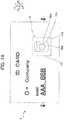
- Figs. 1A and 1B are views illustrating a card 1 of a first embodiment.
- Fig. 1A is a view of the upper surface of the card 1 as viewed from the normal direction (lamination direction of layers forming the card 1).
- a hologram image 41b and a grating shape 52b are shown by solid lines, but as will be described later, the card 1 is configured so that both cannot be simultaneously visually recognized.
- Fig. 1B is a sectional view taken along line B-B of Fig. 1A .
- Fig. 2 is an enlarged view of the inside of the two-dot chain line (part indicated by arrow 2) of Fig. 1B .
- This coordinate system represents a left-right direction X (left side X1 and right side X2), a longitudinal direction Y (lower side Y1 and upper side Y2), and a thickness direction Z with reference to the state of Fig. 1A .
- the thickness of each configuration is exaggeratedly illustrated as appropriate.
- the direction of the thickness direction Z (lower side Z1 and upper side Z2) is determined for convenience of description and does not limit the front and back sides of the card 1.
- the card 1 (laminate) is used as, for example, an ID card.
- the concept of the card is not limited to the ID card or the like, and widely includes a medium having a laminated configuration of the embodiment.
- the card 1 includes a card used for a data page or the like of a passport by providing a non-contact communication IC chip, a loop antenna, a hinge, and the like.
- the external shape of the card 1 may be matched with the size of the passport or the like.
- the laminate may be used, for example, for a cash voucher and a ticket.
- the card 1 includes a base material 11, a laser coloring layer 15, an upper transparent layer 21, a lower transparent layer 22, an embedded member 31, and an optical element 40.
- the upper transparent layer 21, the laser coloring layer 15, the base material 11, and the lower transparent layer 22 are laminated in this order from the upper side Z2 toward the lower side Z1.
- These members can be formed of a resin sheet material such as polycarbonate (PC), polyethylene terephthalate (PET), amorphous PET copolymer (PET-G), polyvinyl chloride (PVC) or the like.
- the combination of the resin sheet materials is not limited.
- the embedded member 31 may be formed of PET and the other layers may be formed of PC.
- the base material 11 constitutes the base material of the card 1.
- the base material 11 may be a multilayer.
- the color of the base material 11 is white.
- the base material 11 includes an upper printed layer 11a and a lower printed layer 11b.
- the upper printed layer 11a and the lower printed layer 11b are respectively provided on the upper surface and the lower surface of the base material 11.
- common information that is, information common to card owners is printed.
- the common information is, for example, text information such as "ID CARD” and "OX Company", or a pattern (not illustrated) such as ground pattern.
- the upper printed layer 11a can be formed by, for example, offset printing.
- the common information is also printed in the lower printed layer 11b.
- the information in the upper printed layer 11a is visible through the laser coloring layer 15 and the upper transparent layer 21.
- the information in the lower printed layer 11b is visible through the lower transparent layer 22.
- the base material 11 is an accommodating layer that accommodates the embedded member 31. That is, the base material 11 includes an accommodating portion 13.
- the area of the accommodating portion 13, that is, the installation range of the embedded member 31 is entirely formed by a layer which is transparent in the thickness direction Z. Therefore, when viewed from the upper side Z2, the area of the accommodating portion 13 is a transparent window 3.
- the accommodating portion 13 is a hole that accommodates the embedded member 31.
- the shape of the accommodating portion 13 as viewed from the upper side Z2 is quadrangular, the shape is not limited thereto and may be, for example, circular.
- the inner surface of the accommodating portion 13 is a reflection wall 13a (reflection portion) that reflects light toward the inside of the embedded member 31.
- the reflection wall 13a has the color (that is, white) of the base material 11, and the embedded member 31 is transparent. Therefore, the light reflected at the reflection wall 13a, which is the interface between the base material 11 and the embedded member 31, is reflected toward the inside of the embedded member 31 and then travels to the inside of the embedded member 31. Details of the travel of the light will be described later. In a state viewed from the upper side Z2, the reflection wall 13a is positioned outside a diffraction grating 52a (described later).
- the laser coloring layer 15 is a layer having light-transmitting properties.
- the laser coloring layer 15 contains a color developer. Therefore, the range of the laser coloring layer 15 irradiated with laser light generates heat and develops in black, whereby laser marking is achieved.
- the above color development is also referred to as "laser print, laser printing", or the like.
- the material of the laser coloring layer 15 may not contain a color developer as long as the laser coloring layer 15 develops color by being irradiated with laser light.
- the developed color may be other than black.
- individual information of the owner of the card is printed. In the example of Fig. 1 , the individual information is the name "AAA BBB" of the card owner.
- the information laser-printed in the laser coloring layer 15 is visible through the upper transparent layer 21.
- the upper transparent layer 21 is a layer having light-transmitting properties.
- the upper transparent layer 21 is a layer that protects the laser coloring layer 15 and the like.
- the lower transparent layer 22 is a layer similar to the upper transparent layer 21, has light-transmitting properties, and is a layer that protects the base material 11 and the like.
- the lower surface and the upper surface of the upper transparent layer 21 and the lower surface and the upper surface of the lower transparent layer 22 may be provided with a printed layer as necessary. In this case, these printed layers are provided outside the installation range of the embedded member 31 in a state viewed from the upper side Z2. This is to prevent the light incident on the embedded member 31 from being disturbed.
- these printed layers may be provided within the installation range of the embedded member 31 as long as printed layers transmit light corresponding to the diffraction grating 52a (described later) of a diffraction grating forming layer 52.
- these printed layers may be provided within the installation range of the embedded member 31 as long as the printed layers transmit the wavelength for green.
- the embedded member 31 is a transparent member and has light-transmitting properties.
- the embedded member 31 is formed of a single layer of a resin sheet material similar to the upper transparent layer 21 or the like, or a plurality of these layers.
- the external shape (length in each of the left-right direction X, the longitudinal direction Y, and the thickness direction Z) of the embedded member 31 has a size that just fits in the accommodating portion 13. Accordingly, the embedded member 31 is embedded in the resin layers (the base material 11, the laser coloring layer 15, and the lower transparent layer 22) forming the card 1.
- a form in which a slight gap is provided between the embedded member 31 and the reflection wall 13a of the accommodating portion 13 may be adopted. This is because, even in this form, the reflection wall 13a can reflect light toward the inside the embedded member 31.
- a heat seal layer may be provided on the lower surface of the embedded member 31.
- a HS layer may be provided on the upper surface of the embedded member 31 to adhere the embedded member 31 and the laser coloring layer 15 to each other.
- the optical element 40 is a layer optically functioning by a hologram and diffraction.
- the external shape of the optical element 40 and the external shape of the embedded member 31 are the same.
- the external shapes of the two are not limited thereto and may be different from each other.
- the optical element 40 includes a hologram layer 41, a diffraction grating layer 50, and HS layers 61 and 62. These layers are transparent layers and the entire optical element 40 is also transparent.
- the HS layer 61, the hologram layer 41, the diffraction grating layer 50, and the HS layer 62 are laminated in this order from the upper side Z2 toward the lower side Z1.
- the hologram layer 41 is a transparent hologram layer.
- types of holograms include a Lippmann hologram and an embossed hologram.
- a Lippmann hologram is suitable.
- the hologram image 41b is an image of a cylinder. In a state viewed from the upper side Z2, the hologram image 41b is located in the accommodating portion 13 (see Fig. 1A ).
- the hologram image 41b is set to reflect light toward the front surface when the incident angle of the light is 45°. Therefore, an observer can observe the hologram image 41b by causing light such as an indoor lighting 4 to be incident on the window 3 at an incident angle of 45° in a state in which the card 1 is observed from the upper side Z2.
- the angle between the thickness direction Z and the observation direction of the hologram image 41b is also referred to as an observation angle ⁇ 41b.
- the observation angle ⁇ 41b has a width of about 10°. Therefore, the observer can observe the hologram image 41b within an observation range at an angle of about 10° from the front surface of the hologram image 41b.
- the diffraction grating layer 50 includes a diffraction grating base material 51, the diffraction grating forming layer 52, and a high refractive index layer 53.
- the diffraction grating base material 51, the diffraction grating forming layer 52, and the high refractive index layer 53 are overlapped in this order from the upper side Z2 toward the lower side Z1.
- the diffraction grating base material 51 is a base material for forming the diffraction grating 52a.
- the diffraction grating base material 51 is formed of a sheet material similar to the upper transparent layer 21 and the like.
- a transparent HS layer or the like may be provided between the diffraction grating base material 51 and the hologram layer 41 in order to adhere the diffraction grating base material 51 and the hologram layer 41 to each other.
- the diffraction grating forming layer 52 is a layer in which the diffraction grating 52a is formed.
- the diffraction grating 52a is formed by forming the lower surface of the diffraction grating forming layer 52 in an uneven shape.
- the diffraction grating 52a causes light (also referred to as "arrival light") that has arrived at the diffraction grating 52a through a light guide layer (described later) to exit toward the diffraction grating base material 51.
- the diffraction grating 52a causes, in the arrival light, light having an incident angle ⁇ 52a from the diffraction grating 52a to the high refractive index layer 53 and a specific wavelength to exit.
- the incident angle ⁇ 52a is set to 45°.
- the incident angle ⁇ and the wavelength may have specific ranges.
- the wavelength of the exiting light varies depending on the period of the recesses and protrusions of the diffraction grating 52a. Accordingly, the diffraction grating 52a can cause light having a specific color (for example, green) to exit.
- the diffraction grating 52a has an optical function of causing, in arrival light L54 and L55, light having a specific incident angle ⁇ and a specific wavelength to exit.
- the diffracted light is also referred to as diffracted light.
- the diffraction grating 52a can be formed, for example, by preparing a plate precursor having a periodic structure and shaping the plate precursor in the diffraction grating forming layer 52.
- a resin material that has been used in an embossed hologram or the like for example, a cured product of a curable resin such as a resin, an ultraviolet curable resin, or an ionizing radiation curable resin, a thermoplastic resin, and the like can be used.
- the shape (hereinafter, also referred to as "grating shape”) of the installation range of the diffraction grating 52a is a star shape.
- the grating shape 52b is located inside the region where the accommodating portion 13 is provided.
- the grating shape 52b is smaller than the external shape of the hologram image 41b, is located in the hologram image 41b, and overlaps the hologram image 41b. That is, the hologram image 41b covers the grating shape 52b.
- the hologram image 41b and shape 52b are not limited thereto and may not be overlapped.
- the high refractive index layer 53 is a thin film covering the lower surface of the diffraction grating forming layer 52.
- the high refractive index layer 53 is disposed immediately under the diffraction grating forming layer 52 and is thus in direct contact with the lower surface of the diffraction grating forming layer 52.
- the refractive index of the high refractive index layer 53 is larger than the refractive indexes of the other layers (the diffraction grating forming layer 52 and the like.
- the high refractive index layer 53 can be formed, for example, by forming a material such as a metal such as Mg, Ti, Cr, Fe, Co, Ni, Cu, Zn, Ga, Ge, Se, Rb, Pd, Ag, Cd, In, Sn, Sb, Te, Au, Pb, or Bi, an oxide of the metal, or a sulfide of the metal such as ZnS on the diffraction grating forming layer 52 by a vacuum deposition method.
- a material such as a metal such as Mg, Ti, Cr, Fe, Co, Ni, Cu, Zn, Ga, Ge, Se, Rb, Pd, Ag, Cd, In, Sn, Sb, Te, Au, Pb, or Bi
- a sulfide of the metal such as ZnS
- the HS layers 61 and 62 are formed of a thermoplastic adhesive (polyester resin or the like) or the like.
- the HS layer 61 adheres the upper transparent layer 21 and the hologram layer 41 to each other.
- the HS layer 62 adheres of the high refractive index layer 53 and the lower transparent layer 22 to each other.
- the layer configuration in the region of the window 3, the upper transparent layer 21, the HS layer 61, the hologram layer 41, the diffraction grating base material 51, the diffraction grating forming layer 52, the high refractive index layer 53, the HS layer 62, the laser coloring layer 15, the embedded member 31, and the lower transparent layer 22 are arranged in this order.
- normal observation refers to a state in which the observer observes the card 1 from the upper surface and light L41 from the lighting 4, which is a light source, is incident on the card 1 at an incident angle of 45° (an angle corresponding to the hologram image 41b).
- the lighting 4 is, for example, an indoor fluorescent lamp or a light bulb.
- the light L41 is white light, and the light intensity thereof is, for example, at a general indoor brightness.
- the intensity of light is low, diffracted light at an intensity at which the grating shape 52b is visually recognized is not generated.
- the incident angle is small, the embedded member 31 and the like cannot sufficiently function as a light guide layer as described later. Therefore, the grating shape 52b cannot be visually recognized.
- the hologram image 41b is larger than the grating shape 52b which is the shape of the installation range of the diffraction grating 52a.
- the hologram image 41b covers the grating shape 52b and light is less likely to directly hit the diffraction grating 52a, so that it is difficult to visually recognize the grating shape 52b as a thin shadow. Therefore, the hologram image 41b can hide the diffraction grating 52a.
- the light L41 incident on the upper transparent layer 21 from the outside of the card 1 passes through the HS layer 61 and the hologram layer 41 of the optical element 40 and arrives at the hologram image 41b.
- the hologram image 41b reflects light L42 toward the upper side Z2 within the observation angle ⁇ 41b.
- the hologram layer 41 is one on which the stereoscopic hologram image 41b is recorded. Therefore, by changing the observation angle ⁇ 41b within a range of about 10°, the direction of the cylinder as the reproduced image of the hologram changes.
- Intense lighting observation is a state in which light L51 that is more intense than in normal observation is incident on the transparent window 3 using a pen-shaped light 5 or the like.
- the light L51 is white light.
- the intensity of the light arriving at the reflection wall 13a can be increased.
- the light L51 incident on the upper transparent layer 21 from the outside of the card 1 passes through the upper transparent layer 21, the optical element 40, and the laser coloring layer 15, further passes through the inside of the embedded member 31, and arrives at the reflection wall 13a.
- the light L51 arriving at the reflection wall 13a is irregularly reflected at the reflection wall 13a. Since the reflection wall 13a is white, there is little light absorbed by the reflection wall 13a. Therefore, most of the light L51 arriving at the reflection wall 13a is reflected at the reflection wall 13a and travels to the inside of the embedded member 31.
- the light reflected at the reflection wall 13a travels, for example, as follows.
- the hologram image 41b could not be visually recognized during the intense lighting observation. For example, the following reasons are conceivable.
- the grating shape 52b and the hologram image 41b are observed as follows.
- the grating shape 52b cannot be visually recognized, whereas the hologram image 41b can be visually recognized.
- the intense lighting observation the grating shape 52b can be visually recognized, whereas the hologram image 41b cannot be visually recognized.
- the card 1 can switch between visually recognizable images or the like depending on the lighting state.
- the grating shape 52b cannot be visually recognized in a normal lighting state, and can be visually recognized only by a special observation method called intense lighting observation. Therefore, it is difficult for a person other than the card issuer or the like to recognize the existence of the diffraction grating 52a, so that it is difficult to forge the card. Therefore, the card 1 has high security.
- the card 1 can be checked by switching between the hologram image 41b and the grating shape 52b by changing and observing the lighting state, authenticity can be determined.
- the light L53 after being diffracted by the diffraction grating 52a exits within the range of the observation angle ⁇ 41b of the hologram image 41b. Therefore, the observer can check the grating shape 52b by switching to the intense lighting observation with the pen-shaped light 5 or the like while maintaining the posture in which the hologram image 41b is observed in the normal lighting state. Accordingly, workability for authenticity determination is good.
- Figs. 3A and 3B are sectional views illustrating a method of manufacturing the card 1 of the first embodiment.
- Fig. 3A is a view illustrating a hot pressing process.
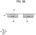
- Fig. 3B is a view illustrating a form in which a plurality of the optical elements 40 are held by a carrier film 45.
- the card 1 can be manufactured by hot pressing.
- the card 1 can be manufactured according to the following steps. The following procedure may be changed as appropriate.
- the optical element 40, the embedded member 31, and the base material 11 are manufactured as follows.
- the base material 11 is provided with a hole 13b for forming the accommodating portion 13 by press working or the like.
- the diffraction grating layer 50 is manufactured by laminating the diffraction grating forming layer 52 and the high refractive index layer 53 in this order on the lower surface of the diffraction grating base material 51. Thereafter, the hologram layer 41 and the diffraction grating layer 50 are adhered to each other by an HS layer or the like. Thereafter, the HS layers 61 and 62 are respectively provided on the upper surface of the hologram layer 41 and the lower surface of the diffraction grating layer 50.
- the optical elements 40 may be formed by manufacturing a single sheet in which a plurality of optical element layers are arranged (so-called multi-faced) in the surface direction (XY plane direction) and then dividing the single sheet into individual pieces by pressing or the like.
- the plurality of individual optical elements 40 may be held by the carrier film 45 such as PET.
- the carrier film 45 such as PET.
- an adhesive layer having a weak holding force may be provided on the carrier film 45, or the adhesion of the HS layer 61 may be used.
- the HS layer 61 one having weak adhesiveness even at room temperature may be selected.
- the outer wall of the embedded member 31 and the reflection wall 13a of the accommodating portion 13 are thermally welded to each other.
- the outer wall of the embedded member 31 and the reflection wall 13a of the accommodating portion 13 are not thermally welded to each other.
- the reflection wall 13a may exhibit a function of guiding light to the inside of the embedded member 31 by reflecting light. Therefore, the outer wall of the embedded member 31 and the reflection wall 13a of the accommodating portion 13 may be thermally welded or may not be thermally welded to each other. Furthermore, these may be in close contact with each other, or may have a gap therebetween.
- the cards 1 in which members of a plurality of the cards 1 are arranged in the surface direction may be manufactured and then divided into individual pieces, but a detailed description will be omitted.
- variable information is laser-printed by performing laser irradiation.
- the card 1 of this embodiment can be switched between the hologram image 41b and the grating shape 52b depending on the lighting state. Accordingly, authenticity can be determined. Furthermore, by providing the hologram and the diffraction grating in the card 1, the security thereof can be improved.
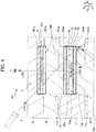
- Fig. 4 is a sectional view (view corresponding to Fig. 2 ) illustrating a card 201 of the second embodiment.
- the hologram layer 41 and the diffraction grating layer 50 are separated from each other.
- the layer configurations of the hologram layer 41 and the diffraction grating layer 50 are the same as those of the first embodiment.
- the laser coloring layer 15 and an embedded member 231a are disposed between the hologram layer 41 and the diffraction grating layer 50.
- the form in which the hologram layer and the diffraction grating layer are separated from each other is also included in the concept of the optical element.
- the upper and lower surfaces of the hologram layer 41 are provided with transparent HS layers 261a and 261b.
- the HS layer 261a adheres the upper transparent layer and the hologram layer 41 to each other.
- the HS layer 261b adheres the hologram layer 41 and the laser coloring layer 15 to each other.
- the diffraction grating layer 50 is accommodated in the accommodating portion 13. Therefore, in the accommodating portion 13, the embedded member 231a, the diffraction grating layer 50, and an embedded member 231b are arranged from the upper side Z2 toward the lower side Z1.
- the embedded members 231a and 231b are members similar to the embedded member of the first embodiment and are transparent.
- the upper and lower surfaces of the diffraction grating layer 50 are provided with transparent HS layers 262a and 262b.
- the HS layer 262a adheres the embedded member 231a and the diffraction grating base material 51 to each other.
- the HS layer 262b adheres the high refractive index layer 53 and the embedded member 231b to each other.
- the hologram image 41b can be visually recognized, whereas the grating shape cannot be visually recognized. In the intense lighting observation, as in the first embodiment, the hologram image 41b cannot be visually recognized.
- light L251 such as the pen-shaped light 5 passes through the upper transparent layer 21, the hologram layer 41, the laser coloring layer 15, the embedded member 231a, the diffraction grating layer 50, the embedded member 231b, and arrives at the reflection wall 13a.
- the light L251 arriving at the reflection wall 13a is irregularly reflected, then passes through the light guide layer, and is incident on the diffraction grating 52a as arrival light L254.
- the lower transparent layer 22, the embedded member 231b, the HS layer 262b, and the like mainly function as the light guide layer.
- the travel of the light is complex as in the first embodiment.
- the diffraction grating layer 50 is accommodated in the accommodating portion 13, the entire circumference of the diffraction grating 52a is surrounded by the reflection wall 13a. Accordingly, the intensity of light arriving at the diffraction grating 52a can be increased.
- the arrival light L254 is diffracted by the function of the diffraction grating 52a, then passes through the diffraction grating base material 51, the embedded member 231a, the laser coloring layer 15, the hologram layer 41, the upper transparent layer 21, and the like, and exits as light L256. Accordingly, in the intense lighting observation, the grating shape can be visually recognized.
- the layers may be laminated and hot pressed.
- the embedded member 231a, the diffraction grating layer 50, and the embedded member 231b may be hot pressed into an assembly in which the layers are adhered to one another, before being inserted into the accommodating portion 13. Accordingly, the diffraction grating 52a is not exposed to the outside, and thus the diffraction grating 52a can be protected from being contaminated during handling (during storage, transporting, or the like) of a single component.
- the hologram image 41b and the grating shape can be observed.
- Figs. 5A and 5B are views (view corresponding to Figs. 1A and 1B ) illustrating a card 301 of a third embodiment.
- Fig. 5A is a view of the upper surface of the card 301 as viewed from the normal direction.
- Fig. 5B is a sectional view taken along line B-B of Fig. 1A .
- the optical element 40 is the same as that in the first embodiment, and the configuration of the base material is different from that in the first embodiment.
- the base material of the card 301 is a transparent base material 311.
- the card 301 does not have an embedded member. Therefore, the transparent base material 311 does not have an accommodating hole and is disposed on the entire surface between the laser coloring layer 15 and the lower transparent layer 22.
- the upper and lower surfaces of the transparent base material 311 are respectively provided with an upper printed layer 311a and a lower printed layer 311b.
- the upper printed layer 311a is a white solid printed layer.
- a partial range and a range in which the optical element 40 is disposed in the upper printed layer 311a are removed.
- the ranges respectively form windows 303a and 303b.
- the window 303a has a function as an introduction portion through which light is introduced into the transparent base material (light guide layer) 311.
- the window 303b has a function as an exit portion that causes the light introduced through the window 303a and is guided by the transparent base material (light guide layer) 311 to exit toward the diffraction grating 52a.
- the lower printed layer 311b is a solid printed layer in which the entire surface is white.
- the thickness of each layer in the third embodiment will be described.
- the thickness of the upper transparent layer 21 is desirably 5 ⁇ m or more and 500 ⁇ m or less, and is set to 100 ⁇ m in this embodiment.
- the thickness of the laser coloring layer 15 is desirably 5 ⁇ m or more and 500 ⁇ m or less, and is set to 100 ⁇ m in this embodiment.
- the thickness of the upper printed layer 311a is desirably 5 ⁇ m or more and 500 ⁇ m or less, and is set to 100 ⁇ m in this embodiment.
- the thickness of the transparent base material 311 is desirably 5 ⁇ m or more and 1000 ⁇ m or less, and in this embodiment, the thickness is set to 200 ⁇ m.
- the thickness of the lower printed layer 311b is desirably 5 ⁇ m or more and 500 ⁇ m or less, and is set to 100 ⁇ m in this embodiment.
- the thickness of the lower transparent layer 22 is desirably 5 ⁇ m or more and 500 ⁇ m or less, and is set to 100 ⁇ m in this embodiment.
- the thickness of the optical element (including the light guide film and the hologram) 40 is desirably 10 ⁇ m or more and 1000 ⁇ m or less, and is set to 50 ⁇ m to 100 ⁇ m in this embodiment.
- the grating shape 52b and the hologram image 41b are observed as in the first embodiment.
- light L351 such as the pen-shaped light 5 is caused to be incident on the transparent window 303a.
- the light L351 is repeatedly reflected at the interface between the transparent base material 311 and the lower transparent layer 22 and the interface between the transparent base material 311 and the laser coloring layer 15, and is guided toward the window 303b side.
- the transparent base material 311 functions as a light guide layer.
- the upper printed layer 311a and the lower printed layer 311b are white layers, a large portion of light is guided toward the window 303b side.
- Light L354 arriving at the window 303b passes through the laser coloring layer 15 and arrives at the optical element 40.
- the light L354 is diffracted by the diffraction grating 52a and then exits as light L356. Therefore, in the intense lighting observation, the grating shape 52b can be visually recognized.
- the hologram image 41b cannot be visually recognized as in the first embodiment.
- the transparent base material 311 is configured to be larger than the diffraction grating 52a, and the window 303a and the window 303b are arranged apart from each other.
- the position at which light is introduced and the position at which light exits are separated from each other, and for those who do not know usage, it is difficult to find the usage or to understand the structure. Therefore, forgery is difficult and security can be enhanced.
- the grating shape 52b can be visually recognized by guiding the light incident on the window 303a to the window 303b through the inside of the card.
- the configuration in which the incident light arrives at the diffraction grating 52a is not limited to this embodiment and the above-described embodiments.
- the white layers are not limited thereto.
- white resin sheets or the like may be provided.
Landscapes
- Physics & Mathematics (AREA)
- General Physics & Mathematics (AREA)
- Optics & Photonics (AREA)
- Engineering & Computer Science (AREA)
- Manufacturing & Machinery (AREA)
- Electromagnetism (AREA)
- Health & Medical Sciences (AREA)
- General Health & Medical Sciences (AREA)
- Toxicology (AREA)
- Credit Cards Or The Like (AREA)
- Holo Graphy (AREA)
- Diffracting Gratings Or Hologram Optical Elements (AREA)
- Inspection Of Paper Currency And Valuable Securities (AREA)
- Laminated Bodies (AREA)
Abstract
Description
- The present invention relates to an optical element, a laminate, and a booklet capable of optically functioning.
- In the related art, there is a security document provided with a light diffractable hologram or the like (for example, Patent Document 1). For a medium like such a security document, an improvement in security has been required at all times.
- Patent Document 1: Japanese Patent No.
5559354 - An object of the present invention is to provide an optical element, a laminate, and a booklet having improved security.
- The present invention solves the problem by the following solving means. In order to facilitate understanding, reference numerals corresponding to embodiments of the present invention are given for the description, but the present invention is not limited thereto. In addition, configurations described with reference numerals may be modified as appropriate, and at least a part thereof may be replaced by another configuration.
-
- A first invention is an optical element including: a hologram layer (41) on which a hologram image (41b) is recorded; and a diffraction grating layer (50) laminated on one surface side of the hologram layer, in which the diffraction grating layer includes a diffraction grating (52a) having recesses and protrusions in a thickness direction.
- A second invention is the optical element according to the first invention further including a light guide layer that guides light to the diffraction grating is provided on a side which is one surface side of the diffraction grating layer (50) and is opposite to a side on which the hologram layer (41) is disposed.
- A third invention is the optical element according to the second invention, in which the light guide layer (311) is configured as a region larger than the diffraction grating (52a), and the light guide layer includes an introduction portion (303a) through which light is introduced into the light guide layer, and an exit portion (303b) that causes the light introduced through the introduction portion and guided by the light guide layer to exit toward the diffraction grating.
- A fourth invention is the optical element according to the third invention, further including: a printed layer (311a) formed to cover at least a portion of the light guide layer (311), in which the printed layer is configured as a removed portion where ink is not provided, at positions corresponding to the introduction portion (303a) and the exit portion (303b).
- A fifth invention is the optical element according to any one the first to fourth inventions, in which the hologram image (41b) of the hologram layer (41) is larger than a grating shape (52b) which is a shape of an installation range of the diffraction grating (52a) when viewed in a lamination direction and covers the grating shape.
- A sixth invention is the optical element according to any one of the first to fifth inventions, in which the diffraction grating (52a) causes diffracted light to exit to an inside of an observation range of the hologram image (41b) of the hologram layer (41).
- A seventh invention is the optical element according to any one of the first to sixth inventions, further including a high refractive index layer (53) which is in direct contact with the diffraction grating (52a) and has a higher refractive index than a diffraction grating forming layer (52) forming the diffraction grating.
- An eighth invention is A laminate including: the optical element (40, 240) according to any one of the first to seventh inventions.
- A ninth invention is the laminate including the optical element according to the eighth invention, further including a reflection portion (13a) which is located outside the diffraction grating (52a) when viewed in a lamination direction and reflects light inward. A tenth invention is the laminate according to the ninth invention, further including a transparent embedded member (31, 231b) embedded in a resin layer forming the laminate, in which the optical element (40, 240) is disposed above the embedded member, and the reflection portion (13a) is a wall portion surrounding the embedded member. An eleventh invention is the laminate according to any one of the eighth to tenth inventions, in which the laminate is a card (1, 201, 301). A twelfth invention is a booklet including the laminate according to any one of the eighth to tenth inventions.
- According to the present invention, an optical element, a laminate, and a booklet having improved security can be provided.
-
-
Fig. 1A is a view illustrating acard 1 of a first embodiment. -
Fig. 1B is a view illustrating thecard 1 of the first embodiment. -
Fig. 2 is an enlarged view of the inside of the two-dot chain line (part indicated by arrow 2) ofFig. 1B . -
Fig. 3A is a sectional view illustrating a method of manufacturing thecard 1 of the first embodiment. -
Fig. 3B is a sectional view illustrating the method of manufacturing thecard 1 of the first embodiment. -
Fig. 4 is a sectional view (view corresponding toFig. 2 ) illustrating acard 201 of a second embodiment. -
Fig. 5A is a view (view corresponding toFig. 1A ) illustrating acard 301 of a third embodiment. -
Fig. 5B is a view (view corresponding toFig. 1B ) illustrating thecard 301 of the third embodiment. - Hereinafter, embodiments of the present invention will be described with reference to the drawings and the like.
-
Figs. 1A and1B are views illustrating acard 1 of a first embodiment.Fig. 1A is a view of the upper surface of thecard 1 as viewed from the normal direction (lamination direction of layers forming the card 1). InFig. 1A , for convenience sake, ahologram image 41b and agrating shape 52b are shown by solid lines, but as will be described later, thecard 1 is configured so that both cannot be simultaneously visually recognized.Fig. 1B is a sectional view taken along line B-B ofFig. 1A .Fig. 2 is an enlarged view of the inside of the two-dot chain line (part indicated by arrow 2) ofFig. 1B . In order to facilitate description and understanding, an XYZ orthogonal coordinate system is provided in the embodiments and the drawings. This coordinate system represents a left-right direction X (left side X1 and right side X2), a longitudinal direction Y (lower side Y1 and upper side Y2), and a thickness direction Z with reference to the state ofFig. 1A . The thickness of each configuration is exaggeratedly illustrated as appropriate. The direction of the thickness direction Z (lower side Z1 and upper side Z2) is determined for convenience of description and does not limit the front and back sides of thecard 1. - The card 1 (laminate) is used as, for example, an ID card. In the embodiment, the concept of the card is not limited to the ID card or the like, and widely includes a medium having a laminated configuration of the embodiment. For example, the
card 1 includes a card used for a data page or the like of a passport by providing a non-contact communication IC chip, a loop antenna, a hinge, and the like. In this case, the external shape of thecard 1 may be matched with the size of the passport or the like. Furthermore, the laminate may be used, for example, for a cash voucher and a ticket. - The
card 1 includes abase material 11, alaser coloring layer 15, an uppertransparent layer 21, a lowertransparent layer 22, an embeddedmember 31, and anoptical element 40. The uppertransparent layer 21, thelaser coloring layer 15, thebase material 11, and the lowertransparent layer 22 are laminated in this order from the upper side Z2 toward the lower side Z1. These members can be formed of a resin sheet material such as polycarbonate (PC), polyethylene terephthalate (PET), amorphous PET copolymer (PET-G), polyvinyl chloride (PVC) or the like. The combination of the resin sheet materials is not limited. For example, the embeddedmember 31 may be formed of PET and the other layers may be formed of PC. - The
base material 11 constitutes the base material of thecard 1. Thebase material 11 may be a multilayer. The color of thebase material 11 is white. Thebase material 11 includes an upper printedlayer 11a and a lower printedlayer 11b. The upper printedlayer 11a and the lower printedlayer 11b are respectively provided on the upper surface and the lower surface of thebase material 11. In the upper printedlayer 11a, common information, that is, information common to card owners is printed. The common information is, for example, text information such as "ID CARD" and "OX Company", or a pattern (not illustrated) such as ground pattern. The upper printedlayer 11a can be formed by, for example, offset printing. Similarly, the common information is also printed in the lower printedlayer 11b. The information in the upper printedlayer 11a is visible through thelaser coloring layer 15 and the uppertransparent layer 21. The information in the lower printedlayer 11b is visible through the lowertransparent layer 22. - In addition, the
base material 11 is an accommodating layer that accommodates the embeddedmember 31. That is, thebase material 11 includes anaccommodating portion 13. The area of theaccommodating portion 13, that is, the installation range of the embeddedmember 31 is entirely formed by a layer which is transparent in the thickness direction Z. Therefore, when viewed from the upper side Z2, the area of theaccommodating portion 13 is atransparent window 3. Theaccommodating portion 13 is a hole that accommodates the embeddedmember 31. Although the shape of theaccommodating portion 13 as viewed from the upper side Z2 is quadrangular, the shape is not limited thereto and may be, for example, circular. The inner surface of theaccommodating portion 13 is areflection wall 13a (reflection portion) that reflects light toward the inside of the embeddedmember 31. Thereflection wall 13a has the color (that is, white) of thebase material 11, and the embeddedmember 31 is transparent. Therefore, the light reflected at thereflection wall 13a, which is the interface between thebase material 11 and the embeddedmember 31, is reflected toward the inside of the embeddedmember 31 and then travels to the inside of the embeddedmember 31. Details of the travel of the light will be described later. In a state viewed from the upper side Z2, thereflection wall 13a is positioned outside adiffraction grating 52a (described later). - The
laser coloring layer 15 is a layer having light-transmitting properties. Thelaser coloring layer 15 contains a color developer. Therefore, the range of thelaser coloring layer 15 irradiated with laser light generates heat and develops in black, whereby laser marking is achieved. In the embodiment, the above color development is also referred to as "laser print, laser printing", or the like. The material of thelaser coloring layer 15 may not contain a color developer as long as thelaser coloring layer 15 develops color by being irradiated with laser light. The developed color may be other than black. In thelaser coloring layer 15, individual information of the owner of the card is printed. In the example ofFig. 1 , the individual information is the name "AAA BBB" of the card owner. The information laser-printed in thelaser coloring layer 15 is visible through the uppertransparent layer 21. - The upper
transparent layer 21 is a layer having light-transmitting properties. The uppertransparent layer 21 is a layer that protects thelaser coloring layer 15 and the like. The lowertransparent layer 22 is a layer similar to the uppertransparent layer 21, has light-transmitting properties, and is a layer that protects thebase material 11 and the like. The lower surface and the upper surface of the uppertransparent layer 21 and the lower surface and the upper surface of the lowertransparent layer 22 may be provided with a printed layer as necessary. In this case, these printed layers are provided outside the installation range of the embeddedmember 31 in a state viewed from the upper side Z2. This is to prevent the light incident on the embeddedmember 31 from being disturbed. However, these printed layers may be provided within the installation range of the embeddedmember 31 as long as printed layers transmit light corresponding to thediffraction grating 52a (described later) of a diffractiongrating forming layer 52. For example, in a case where thediffraction grating 52a diffracts the wavelength for green, these printed layers may be provided within the installation range of the embeddedmember 31 as long as the printed layers transmit the wavelength for green. - The embedded
member 31 is a transparent member and has light-transmitting properties. The embeddedmember 31 is formed of a single layer of a resin sheet material similar to the uppertransparent layer 21 or the like, or a plurality of these layers. The external shape (length in each of the left-right direction X, the longitudinal direction Y, and the thickness direction Z) of the embeddedmember 31 has a size that just fits in theaccommodating portion 13. Accordingly, the embeddedmember 31 is embedded in the resin layers (thebase material 11, thelaser coloring layer 15, and the lower transparent layer 22) forming thecard 1. However, a form in which a slight gap is provided between the embeddedmember 31 and thereflection wall 13a of theaccommodating portion 13 may be adopted. This is because, even in this form, thereflection wall 13a can reflect light toward the inside the embeddedmember 31. - In a case where the embedded
member 31 and the lowertransparent layer 22 are made of materials that are hard to be thermally welded or the like, a heat seal layer (HS layer) may be provided on the lower surface of the embeddedmember 31. Similarly, a HS layer may be provided on the upper surface of the embeddedmember 31 to adhere the embeddedmember 31 and thelaser coloring layer 15 to each other. - The
optical element 40 is a layer optically functioning by a hologram and diffraction. In a state viewed from the upper side Z2, the external shape of theoptical element 40 and the external shape of the embeddedmember 31 are the same. The external shapes of the two are not limited thereto and may be different from each other. As illustrated inFig. 2 , theoptical element 40 includes ahologram layer 41, adiffraction grating layer 50, and HS layers 61 and 62. These layers are transparent layers and the entireoptical element 40 is also transparent. TheHS layer 61, thehologram layer 41, thediffraction grating layer 50, and theHS layer 62 are laminated in this order from the upper side Z2 toward the lower side Z1. - The
hologram layer 41 is a transparent hologram layer. Examples of types of holograms include a Lippmann hologram and an embossed hologram. In particular, from the viewpoint of stereoscopic image expression of thehologram image 41b and security, a Lippmann hologram is suitable. Thehologram image 41b is an image of a cylinder. In a state viewed from the upper side Z2, thehologram image 41b is located in the accommodating portion 13 (seeFig. 1A ). - In the embodiment, the
hologram image 41b is set to reflect light toward the front surface when the incident angle of the light is 45°. Therefore, an observer can observe thehologram image 41b by causing light such as anindoor lighting 4 to be incident on thewindow 3 at an incident angle of 45° in a state in which thecard 1 is observed from the upper side Z2. In the embodiment, the angle between the thickness direction Z and the observation direction of thehologram image 41b is also referred to as an observation angle θ41b. In the embodiment, the observation angle θ41b has a width of about 10°. Therefore, the observer can observe thehologram image 41b within an observation range at an angle of about 10° from the front surface of thehologram image 41b. - The
diffraction grating layer 50 includes a diffractiongrating base material 51, the diffractiongrating forming layer 52, and a highrefractive index layer 53. The diffractiongrating base material 51, the diffractiongrating forming layer 52, and the highrefractive index layer 53 are overlapped in this order from the upper side Z2 toward the lower side Z1. The diffractiongrating base material 51 is a base material for forming thediffraction grating 52a. The diffractiongrating base material 51 is formed of a sheet material similar to the uppertransparent layer 21 and the like. A transparent HS layer or the like may be provided between the diffractiongrating base material 51 and thehologram layer 41 in order to adhere the diffractiongrating base material 51 and thehologram layer 41 to each other. - The diffraction
grating forming layer 52 is a layer in which thediffraction grating 52a is formed. Thediffraction grating 52a is formed by forming the lower surface of the diffractiongrating forming layer 52 in an uneven shape. - The
diffraction grating 52a causes light (also referred to as "arrival light") that has arrived at the diffraction grating 52a through a light guide layer (described later) to exit toward the diffractiongrating base material 51. Thediffraction grating 52a causes, in the arrival light, light having an incident angle θ52a from thediffraction grating 52a to the highrefractive index layer 53 and a specific wavelength to exit. In the embodiment, the incident angle θ52a is set to 45°. The incident angle θ and the wavelength may have specific ranges. The wavelength of the exiting light varies depending on the period of the recesses and protrusions of thediffraction grating 52a. Accordingly, thediffraction grating 52a can cause light having a specific color (for example, green) to exit. - As described above, the
diffraction grating 52a has an optical function of causing, in arrival light L54 and L55, light having a specific incident angle θ and a specific wavelength to exit. In the embodiment, as an example, an example in which light having an incident angle θ of 45° with respect to the highrefractive index layer 53 is diffracted so as to exit immediately toward the upper side Z2, that is, at an exit angle of 0° is described (seeFig. 2 ). Hereinafter, the diffracted light is also referred to as diffracted light. - The
diffraction grating 52a can be formed, for example, by preparing a plate precursor having a periodic structure and shaping the plate precursor in the diffractiongrating forming layer 52. As the material of the diffractiongrating forming layer 52, a resin material that has been used in an embossed hologram or the like, for example, a cured product of a curable resin such as a resin, an ultraviolet curable resin, or an ionizing radiation curable resin, a thermoplastic resin, and the like can be used. - In a state viewed from the upper side Z2, the shape (hereinafter, also referred to as "grating shape") of the installation range of the
diffraction grating 52a is a star shape. Thegrating shape 52b is located inside the region where theaccommodating portion 13 is provided. In addition, thegrating shape 52b is smaller than the external shape of thehologram image 41b, is located in thehologram image 41b, and overlaps thehologram image 41b. That is, thehologram image 41b covers thegrating shape 52b. In addition, thehologram image 41b andshape 52b are not limited thereto and may not be overlapped. - The high
refractive index layer 53 is a thin film covering the lower surface of the diffractiongrating forming layer 52. The highrefractive index layer 53 is disposed immediately under the diffractiongrating forming layer 52 and is thus in direct contact with the lower surface of the diffractiongrating forming layer 52. The refractive index of the highrefractive index layer 53 is larger than the refractive indexes of the other layers (the diffractiongrating forming layer 52 and the like. The highrefractive index layer 53 can be formed, for example, by forming a material such as a metal such as Mg, Ti, Cr, Fe, Co, Ni, Cu, Zn, Ga, Ge, Se, Rb, Pd, Ag, Cd, In, Sn, Sb, Te, Au, Pb, or Bi, an oxide of the metal, or a sulfide of the metal such as ZnS on the diffractiongrating forming layer 52 by a vacuum deposition method. As the materials of the diffractiongrating forming layer 52 and the highrefractive index layer 53, those having a difference in refractive index between the two so as to cause thediffraction grating 52a to sufficiently function may be appropriately selected. - The HS layers 61 and 62 are formed of a thermoplastic adhesive (polyester resin or the like) or the like. The
HS layer 61 adheres the uppertransparent layer 21 and thehologram layer 41 to each other. TheHS layer 62 adheres of the highrefractive index layer 53 and the lowertransparent layer 22 to each other. - With the layer configuration, in the region of the
window 3, the uppertransparent layer 21, theHS layer 61, thehologram layer 41, the diffractiongrating base material 51, the diffractiongrating forming layer 52, the highrefractive index layer 53, theHS layer 62, thelaser coloring layer 15, the embeddedmember 31, and the lowertransparent layer 22 are arranged in this order. - An observation aspect of the
grating shape 52b andhologram image 41b in a state in which thecard 1 is viewed from the upper side Z2 will be described. In the observation aspect described below, a prototype was prepared and the prototype was actually checked. - As illustrated in
Fig. 2 , normal observation refers to a state in which the observer observes thecard 1 from the upper surface and light L41 from thelighting 4, which is a light source, is incident on thecard 1 at an incident angle of 45° (an angle corresponding to thehologram image 41b). Thelighting 4 is, for example, an indoor fluorescent lamp or a light bulb. The light L41 is white light, and the light intensity thereof is, for example, at a general indoor brightness. - In normal observation, the intensity of light is low, diffracted light at an intensity at which the
grating shape 52b is visually recognized is not generated. In a case where the incident angle is small, the embeddedmember 31 and the like cannot sufficiently function as a light guide layer as described later. Therefore, thegrating shape 52b cannot be visually recognized. - In addition, in normal observation, there may be cases where, even if the
diffraction grating 52a does not function sufficiently, thegrating shape 52b is visually recognizable as a thin shadow. This is because, even in normal observation, a slight difference between the region where thediffraction grating 52a is formed and the other regions in paths through which light passes, transmittance, and the like due to the presence or absence of an uneven shape is a factor. In the embodiment, thehologram image 41b is larger than thegrating shape 52b which is the shape of the installation range of thediffraction grating 52a. Therefore, thehologram image 41b covers thegrating shape 52b and light is less likely to directly hit thediffraction grating 52a, so that it is difficult to visually recognize thegrating shape 52b as a thin shadow. Therefore, thehologram image 41b can hide thediffraction grating 52a. - The light L41 incident on the upper
transparent layer 21 from the outside of thecard 1 passes through theHS layer 61 and thehologram layer 41 of theoptical element 40 and arrives at thehologram image 41b. Thehologram image 41b reflects light L42 toward the upper side Z2 within the observation angle θ41b. As a result, thestereoscopic hologram image 41b is reproduced. Thehologram layer 41 is one on which thestereoscopic hologram image 41b is recorded. Therefore, by changing the observation angle θ41b within a range of about 10°, the direction of the cylinder as the reproduced image of the hologram changes. - Intense lighting observation is a state in which light L51 that is more intense than in normal observation is incident on the
transparent window 3 using a pen-shapedlight 5 or the like. The light L51 is white light. In this case, by increasing the incident angle θ51, the intensity of the light arriving at thereflection wall 13a can be increased. - As illustrated in
Fig. 2 , the light L51 incident on the uppertransparent layer 21 from the outside of thecard 1 passes through the uppertransparent layer 21, theoptical element 40, and thelaser coloring layer 15, further passes through the inside of the embeddedmember 31, and arrives at thereflection wall 13a. The light L51 arriving at thereflection wall 13a is irregularly reflected at thereflection wall 13a. Since thereflection wall 13a is white, there is little light absorbed by thereflection wall 13a. Therefore, most of the light L51 arriving at thereflection wall 13a is reflected at thereflection wall 13a and travels to the inside of the embeddedmember 31. The light reflected at thereflection wall 13a travels, for example, as follows. - (1) Light L52 which is a portion of the irregularly reflected light passes through the embedded
member 31 and the lowertransparent layer 22, and is then reflected at aninterface 22a between the lowertransparent layer 22 and the outside air. Thereafter, the light L52 passes through the lowertransparent layer 22 and the embeddedmember 31 and arrives at thereflection wall 13a again. Also in this case, most of light L53 arriving at thereflection wall 13a is reflected at thereflection wall 13a. Thereafter, the light L54 reflected at thereflection wall 13a passes through the embeddedmember 31, thelaser coloring layer 15, theHS layer 62, and the highrefractive index layer 53, and is incident on thediffraction grating 52a as the arrival light. - (2) The light L55 which is another portion of the irregularly reflected light passes through the embedded
member 31, thelaser coloring layer 15, theHS layer 62, the highrefractive index layer 53, and is incident on thediffraction grating 52a as the arrival light.
As described above, the light reflected at thereflection wall 13a is guided to inside of thelaser coloring layer 15, the embeddedmember 31, the lowertransparent layer 22, the highrefractive index layer 53, theHS layer 62, and the like and arrives at thediffraction grating 52a as the arrival light L54 and L55. In practice, the travel of the light in these layers (that is, thelaser coloring layer 15, the embeddedmember 31, the lowertransparent layer 22, the highrefractive index layer 53, and theHS layer 62, which are transparent layers positioned on the lower side Z1 below the diffractiongrating forming layer 52 and are arranged on the side opposite to the side on which thehologram layer 41 is disposed) is complex. In the embodiment, regardless of which path the light reflected at thereflection wall 13a travels through these layers, these layers function as a light guide layer that guides the light to thediffraction grating 52a.
For example, the light arrives at thediffraction grating 52a by being repeatedly reflected at thereflection wall 13a many times. In addition, the light is repeatedly reflected at each interface. The difference in refractive index between the highrefractive index layer 53 and the diffractiongrating forming layer 52 is large. Similarly, the difference in refractive index between the lowertransparent layer 22 and the outside air is large. Therefore, the condition of total reflection tends to be established at theinterface 53a between the highrefractive index layer 53 and the diffractiongrating forming layer 52, and theinterface 22a between the lowertransparent layer 22 and the outside air.
In this manner, the light incident on thewindow 3 arrives at thediffraction grating 52a after being reflected at thereflection wall 13a at least once. In this case, since thereflection wall 13a is white, thereflection wall 13a can reflect more light. - (3) In the arrival light L54 and L55 arriving at the
diffraction grating 52a, light having an incident angle θ42a of 45° is diffracted by the function of thediffraction grating 52a. For example, in a case where the arrival light L54 and L55 is white light and thediffraction grating 52a causes the wavelength for green to exit, the light having the wavelength for green in the arrival light L54 and L55 is diffracted. In this case, as described above, since the light intensity of the arrival light L54 and L55 is high, the light intensity of the diffracted light can also be increased.
In addition, since the diffractiongrating forming layer 52 and the highrefractive index layer 53 have the above-mentioned difference in refractive index, thediffraction grating 52a reliably exhibits its optical function. That is, unlike the embodiment, in a form in which the highrefractive index layer 53 is not provided and the diffractiongrating forming layer 52 and theHS layer 62 are in direct contact with each other, usually, a sufficiently large difference in refractive index between the diffractiongrating forming layer 52 and theHS layer 62 cannot be obtained. The reason is that both are resin layers and have substantially the same refractive index. Therefore, this type ofdiffraction grating 52a cannot reliably exhibit the optical function. - (4) After being incident on the diffraction
grating forming layer 52, the diffracted light passes through thehologram layer 41, theHS layer 61, and the uppertransparent layer 21, and exits toward the outside of thecard 1, that is, into the air as light L56. Here, since thehologram layer 41 is a transparent hologram, the light incident from the lower side Z1 passes through the upper side Z2. In addition, since the region outside thegrating shape 52b of thediffraction grating 52a is transparent, the space on the lower side Z1 below thecard 1 is observed through the region. Accordingly, thegrating shape 52b can be visually recognized. In addition, since the light intensity of the diffracted light is high, the light L56 also increases in intensity. Therefore, thegrating shape 52b glows brightly and can be clearly observed. - In the above description, the form in which the light is incident on the inside of the
card 1 from the upper side Z2 has been described. However, a form in which the light is incident on the inside of thecard 1 from the lower side Z1 may be adopted. Even in this form, the light that has passed through the lowertransparent layer 22 arrives at thereflection wall 13a and travels in the same manner as in (1) to (4). Therefore, in this form, when the embeddedmember 31 is observed from the upper side Z2, thegrating shape 52b can be clearly observed. - In the prototype, the
hologram image 41b could not be visually recognized during the intense lighting observation. For example, the following reasons are conceivable. - Since the incident angle is large, the
hologram image 41b cannot reflect the light within the observation angle θ41b. - The intensity of light traveling toward the upper side Z2 from the lower side Z1 of the
hologram layer 41 increases due to the function of thereflection wall 13a and the light guide layer. Therefore, it becomes difficult to visually recognize thehologram image 41b. Depending on incident conditions of light, light may be reflected by the highrefractive index layer 53. In this case, since the reflected light is scattered, thehologram image 41b is not seen or is hardly seen, and thegrating shape 52b can be visually recognizable. - As described above, in the normal observation and the intense lighting observation, the
grating shape 52b and thehologram image 41b are observed as follows. In the normal observation, thegrating shape 52b cannot be visually recognized, whereas thehologram image 41b can be visually recognized. Contrary to this, in the intense lighting observation, thegrating shape 52b can be visually recognized, whereas thehologram image 41b cannot be visually recognized. - Thus, the
card 1 can switch between visually recognizable images or the like depending on the lighting state. In addition, thegrating shape 52b cannot be visually recognized in a normal lighting state, and can be visually recognized only by a special observation method called intense lighting observation. Therefore, it is difficult for a person other than the card issuer or the like to recognize the existence of thediffraction grating 52a, so that it is difficult to forge the card. Therefore, thecard 1 has high security. In addition, since thecard 1 can be checked by switching between thehologram image 41b and thegrating shape 52b by changing and observing the lighting state, authenticity can be determined. Furthermore, the light L53 after being diffracted by thediffraction grating 52a exits within the range of the observation angle θ41b of thehologram image 41b. Therefore, the observer can check thegrating shape 52b by switching to the intense lighting observation with the pen-shapedlight 5 or the like while maintaining the posture in which thehologram image 41b is observed in the normal lighting state. Accordingly, workability for authenticity determination is good. -
Figs. 3A and3B are sectional views illustrating a method of manufacturing thecard 1 of the first embodiment.Fig. 3A is a view illustrating a hot pressing process.Fig. 3B is a view illustrating a form in which a plurality of theoptical elements 40 are held by acarrier film 45. As illustrated inFig. 3A , thecard 1 can be manufactured by hot pressing. Thecard 1 can be manufactured according to the following steps. The following procedure may be changed as appropriate. As a preliminary step of the hot pressing ofFig. 3A , theoptical element 40, the embeddedmember 31, and thebase material 11 are manufactured as follows. Thebase material 11 is provided with ahole 13b for forming theaccommodating portion 13 by press working or the like. - The
diffraction grating layer 50 is manufactured by laminating the diffractiongrating forming layer 52 and the highrefractive index layer 53 in this order on the lower surface of the diffractiongrating base material 51. Thereafter, thehologram layer 41 and thediffraction grating layer 50 are adhered to each other by an HS layer or the like. Thereafter, the HS layers 61 and 62 are respectively provided on the upper surface of thehologram layer 41 and the lower surface of thediffraction grating layer 50. Theoptical elements 40 may be formed by manufacturing a single sheet in which a plurality of optical element layers are arranged (so-called multi-faced) in the surface direction (XY plane direction) and then dividing the single sheet into individual pieces by pressing or the like. - As illustrated in
Fig. 3B , the plurality of individualoptical elements 40 may be held by thecarrier film 45 such as PET. For the adhesion between theoptical elements 40 and thecarrier film 45, for example, an adhesive layer having a weak holding force may be provided on thecarrier film 45, or the adhesion of theHS layer 61 may be used. In this case, as theHS layer 61, one having weak adhesiveness even at room temperature may be selected. - Subsequently, as illustrated in
Fig. 3A , hot pressing is performed. That is, the following processing is performed. - (1) The embedded
member 31 is inserted into thehole 13b of thebase material 11. - (2) In a state in which the embedded
member 31 inserted into thehole 13b, the uppertransparent layer 21, theoptical element 40, thelaser coloring layer 15, thebase material 11, and the lowertransparent layer 22 are overlapped in order. In order to suppress positional deviation during the lamination of theoptical element 40, theoptical element 40 may be adhered to thelaser coloring layer 15 by theHS layer 62 in advance. In this case, for example, the temperature at which theHS layer 62 reveals adhesiveness may be lower than the temperature at which theHS layer 61 reveals adhesiveness. By selecting the HS layers 61 and 62 having such properties, the adhesiveness of only theHS layer 62 can be revealed at a low temperature and theoptical element 40 and thelaser coloring layer 15 can be adhered to each other. Unlike the above, theoptical element 40 may be adhered to the uppertransparent layer 21 by theHS layer 61 in advance. In this case, the properties of the HS layers 61 and 62 may be reversed from the above. - (3) The laminate overlapped as in (2) is sandwiched between
hot press plates transparent layer 21 and thehologram layer 41 are adhered to each other with theHS layer 61 interposed therebetween. In addition, thelaser coloring layer 15 and the highrefractive index layer 53 are to each other with theHS layer 62 interposed therebetween. - In a case where the material of the embedded
member 31 and the material of thebase material 11 are easily thermally welded to each other, the outer wall of the embeddedmember 31 and thereflection wall 13a of theaccommodating portion 13 are thermally welded to each other. On the other hand, in a case where the material of the embeddedmember 31 and the material of thebase material 11 are not thermally welded to each other, the outer wall of the embeddedmember 31 and thereflection wall 13a of theaccommodating portion 13 are not thermally welded to each other. However, as described above, thereflection wall 13a may exhibit a function of guiding light to the inside of the embeddedmember 31 by reflecting light. Therefore, the outer wall of the embeddedmember 31 and thereflection wall 13a of theaccommodating portion 13 may be thermally welded or may not be thermally welded to each other. Furthermore, these may be in close contact with each other, or may have a gap therebetween. - Also in the steps (1) to (3), the
cards 1 in which members of a plurality of thecards 1 are arranged in the surface direction may be manufactured and then divided into individual pieces, but a detailed description will be omitted. (4) When the card is issued, variable information is laser-printed by performing laser irradiation. - As described above, the
card 1 of this embodiment can be switched between thehologram image 41b and thegrating shape 52b depending on the lighting state. Accordingly, authenticity can be determined. Furthermore, by providing the hologram and the diffraction grating in thecard 1, the security thereof can be improved. - Next, a second embodiment of the present invention will be described. In the following description and the drawings, like elements which have the same function as those of the first embodiment are denoted by like reference numerals or the ends (last two digits) thereof are denoted by like reference numerals as appropriate, and an overlapping description will be omitted as appropriate.
Fig. 4 is a sectional view (view corresponding toFig. 2 ) illustrating acard 201 of the second embodiment. In theoptical element 240 of this embodiment, thehologram layer 41 and thediffraction grating layer 50 are separated from each other. The layer configurations of thehologram layer 41 and thediffraction grating layer 50 are the same as those of the first embodiment. Thelaser coloring layer 15 and an embeddedmember 231a are disposed between thehologram layer 41 and thediffraction grating layer 50. In the embodiment, as described above, the form in which the hologram layer and the diffraction grating layer are separated from each other is also included in the concept of the optical element. - The upper and lower surfaces of the
hologram layer 41 are provided withtransparent HS layers HS layer 261a adheres the upper transparent layer and thehologram layer 41 to each other. TheHS layer 261b adheres thehologram layer 41 and thelaser coloring layer 15 to each other. - The
diffraction grating layer 50 is accommodated in theaccommodating portion 13. Therefore, in theaccommodating portion 13, the embeddedmember 231a, thediffraction grating layer 50, and an embeddedmember 231b are arranged from the upper side Z2 toward the lower side Z1. The embeddedmembers diffraction grating layer 50 are provided withtransparent HS layers HS layer 262a adheres the embeddedmember 231a and the diffractiongrating base material 51 to each other. TheHS layer 262b adheres the highrefractive index layer 53 and the embeddedmember 231b to each other. - Although not illustrated, in normal observation, as in the first embodiment, the
hologram image 41b can be visually recognized, whereas the grating shape cannot be visually recognized. In the intense lighting observation, as in the first embodiment, thehologram image 41b cannot be visually recognized. On the other hand, as shown inFig. 4 , light L251 such as the pen-shapedlight 5 passes through the uppertransparent layer 21, thehologram layer 41, thelaser coloring layer 15, the embeddedmember 231a, thediffraction grating layer 50, the embeddedmember 231b, and arrives at thereflection wall 13a. As in the first embodiment, the light L251 arriving at thereflection wall 13a is irregularly reflected, then passes through the light guide layer, and is incident on thediffraction grating 52a as arrival light L254. In this case, the lowertransparent layer 22, the embeddedmember 231b, theHS layer 262b, and the like mainly function as the light guide layer. In the light guide layer, the travel of the light is complex as in the first embodiment. In addition, since thediffraction grating layer 50 is accommodated in theaccommodating portion 13, the entire circumference of thediffraction grating 52a is surrounded by thereflection wall 13a. Accordingly, the intensity of light arriving at thediffraction grating 52a can be increased. - Thereafter, the arrival light L254 is diffracted by the function of the
diffraction grating 52a, then passes through the diffractiongrating base material 51, the embeddedmember 231a, thelaser coloring layer 15, thehologram layer 41, the uppertransparent layer 21, and the like, and exits as light L256. Accordingly, in the intense lighting observation, the grating shape can be visually recognized. - In a case where the
card 201 of this embodiment is manufactured, after inserting the embeddedmember 231a, thediffraction grating layer 50, and the embeddedmember 231b into theaccommodating portion 13, the layers may be laminated and hot pressed. The embeddedmember 231a, thediffraction grating layer 50, and the embeddedmember 231b may be hot pressed into an assembly in which the layers are adhered to one another, before being inserted into theaccommodating portion 13. Accordingly, thediffraction grating 52a is not exposed to the outside, and thus thediffraction grating 52a can be protected from being contaminated during handling (during storage, transporting, or the like) of a single component. - As described above, in the
optical element 240 of thecard 201 of this embodiment, even in a form in which thehologram layer 41 and thediffraction grating layer 50 are separated from each other, as in the first embodiment, thehologram image 41b and the grating shape can be observed. -
Figs. 5A and5B are views (view corresponding toFigs. 1A and1B ) illustrating acard 301 of a third embodiment.Fig. 5A is a view of the upper surface of thecard 301 as viewed from the normal direction.Fig. 5B is a sectional view taken along line B-B ofFig. 1A . In thecard 301, theoptical element 40 is the same as that in the first embodiment, and the configuration of the base material is different from that in the first embodiment. The base material of thecard 301 is atransparent base material 311. In addition, thecard 301 does not have an embedded member. Therefore, thetransparent base material 311 does not have an accommodating hole and is disposed on the entire surface between thelaser coloring layer 15 and the lowertransparent layer 22. - The upper and lower surfaces of the
transparent base material 311 are respectively provided with an upper printedlayer 311a and a lower printedlayer 311b. The upper printedlayer 311a is a white solid printed layer. However, a partial range and a range in which theoptical element 40 is disposed in the upper printedlayer 311a are removed. The ranges respectively formwindows window 303a has a function as an introduction portion through which light is introduced into the transparent base material (light guide layer) 311. In addition, thewindow 303b has a function as an exit portion that causes the light introduced through thewindow 303a and is guided by the transparent base material (light guide layer) 311 to exit toward thediffraction grating 52a. The lower printedlayer 311b is a solid printed layer in which the entire surface is white. Here, the thickness of each layer in the third embodiment will be described. The thickness of the uppertransparent layer 21 is desirably 5 µm or more and 500 µm or less, and is set to 100 µm in this embodiment. The thickness of thelaser coloring layer 15 is desirably 5 µm or more and 500 µm or less, and is set to 100 µm in this embodiment. The thickness of the upper printedlayer 311a is desirably 5 µm or more and 500 µm or less, and is set to 100 µm in this embodiment. The thickness of thetransparent base material 311 is desirably 5 µm or more and 1000 µm or less, and in this embodiment, the thickness is set to 200 µm. The thickness of the lower printedlayer 311b is desirably 5 µm or more and 500 µm or less, and is set to 100 µm in this embodiment. The thickness of the lowertransparent layer 22 is desirably 5 µm or more and 500 µm or less, and is set to 100 µm in this embodiment. In addition, the thickness of the optical element (including the light guide film and the hologram) 40 is desirably 10 µm or more and 1000 µm or less, and is set to 50 µm to 100 µm in this embodiment. - In the normal observation, the
grating shape 52b and thehologram image 41b are observed as in the first embodiment. As illustrated inFig. 5B , in the intense lighting observation, light L351 such as the pen-shapedlight 5 is caused to be incident on thetransparent window 303a. The light L351 is repeatedly reflected at the interface between thetransparent base material 311 and the lowertransparent layer 22 and the interface between thetransparent base material 311 and thelaser coloring layer 15, and is guided toward thewindow 303b side. As described above, thetransparent base material 311 functions as a light guide layer. In addition, since the upper printedlayer 311a and the lower printedlayer 311b are white layers, a large portion of light is guided toward thewindow 303b side. - Light L354 arriving at the
window 303b passes through thelaser coloring layer 15 and arrives at theoptical element 40. As in the first embodiment, the light L354 is diffracted by thediffraction grating 52a and then exits as light L356. Therefore, in the intense lighting observation, thegrating shape 52b can be visually recognized. On the other hand, in the intense lighting observation, thehologram image 41b cannot be visually recognized as in the first embodiment. Furthermore, in thecard 301 of this embodiment, thetransparent base material 311 is configured to be larger than thediffraction grating 52a, and thewindow 303a and thewindow 303b are arranged apart from each other. Therefore, the position at which light is introduced and the position at which light exits (the position at which thediffraction grating 52a is disposed) are separated from each other, and for those who do not know usage, it is difficult to find the usage or to understand the structure. Therefore, forgery is difficult and security can be enhanced. - As described above, in the
card 301 of this embodiment, thegrating shape 52b can be visually recognized by guiding the light incident on thewindow 303a to thewindow 303b through the inside of the card. The configuration in which the incident light arrives at thediffraction grating 52a is not limited to this embodiment and the above-described embodiments. In this embodiment, an example in which the upper printedlayer 311a and the lower printedlayer 311b are provided as white layers is described, but the white layers are not limited thereto. For example, white resin sheets or the like may be provided. - While the embodiments of the present invention have been described above, the present invention is not limited to the above-described embodiments. For example, various modifications and changes can be made as in modification embodiments described below and the like, and these are also within the technical scope of the present invention. In addition, the effects described in the embodiments are merely listed as the most preferable effects caused by the present invention, and the effects of the present invention are not limited to those described in the embodiments. The above-described embodiment and modification embodiments described below can be used in combination as appropriate, and a detailed description thereof will be omitted.
-
- (1) In the embodiments, an example in which the color of the incident light and the color of the reflection wall (the color of the base material) are both white is described, but the colors are not limited thereto. The combination of the colors can be selected as appropriate according to the function of the diffraction grating. For example, in a case where the diffraction grating functions at the wavelength for green, the combination of the colors may be set so that the arrival light includes the wavelength for green. Alternatively, the incident light may be white and the reflection wall may be green. In this case, the arrival light at the wavelength for green arrives at the diffraction grating. In addition, in the arrival light, light having an incident angle corresponding to the function of the diffraction grating can be diffracted and exit.
Furthermore, in the embodiments, an example in which the color of the base material is white, that is, the color corresponding to the function of the diffraction grating is described, but the color is not limited thereto. The reflection wall may be configured to reflect light regardless of the color of the base material. For example, the base material may be transparent, and the reflection wall may be colored to a color corresponding to the function of the diffraction grating by coating or the like. - (2) In the embodiments, an example in which the diffraction
grating base material 51, the diffractiongrating forming layer 52, and the highrefractive index layer 53 are arranged from the upper side toward the lower side is described, but the arrangement is not limited thereto. A form in which the highrefractive index layer 53, the diffractiongrating forming layer 52, and the diffractiongrating base material 51 are arranged from the upper side toward the lower side may be adopted. In this form, the diffractiongrating base material 51 functions as the light guide layer that guides light to the diffraction grating. In a case where the highrefractive index layer 53 and the diffractiongrating forming layer 52 are members that can be transferred to other layers, a form in which the diffractiongrating base material 51 is removed may be adopted. That is, thediffraction grating layer 50 may not be provided with a base material such as the diffractiongrating base material 51, and may be a foil or the like having the highrefractive index layer 53 and the diffractiongrating forming layer 52. - (3) In the embodiment, an example in which intense lighting observation is performed using the pen-shaped
light 5 is described. The intense lighting observation is not limited thereto, and for example, a light source attached to a portable device such as a smartphone may be used, or a light source device dedicated to authenticity determination may be used. As the type of the light source, for example, a light emitting diode (LED) light source may be used, an organic light emitting diode (OLED) may be used, or a laser light source may be used. Furthermore, the light emitted by the light source is not limited to white light, and may be light of a specific color such as green. - (4) In the embodiment, an example in which the laminate constitutes the card is described. The laminate is not limited thereto, and for example, the laminate may constitute at least one page of a booklet having a plurality of pages.
-
- 1, 201, 301
- CARD
- 3, 303a, 303b
- WINDOW
- 11
- BASE MATERIAL
- 11a, 311a
- UPPER PRINTED LAYER
- 11b, 311b
- LOWER PRINTED LAYER
- 13
- ACCOMMODATING PORTION
- 13a
- REFLECTION WALL
- 15
- LASER COLORING LAYER
- 21
- UPPER TRANSPARENT LAYER
- 22
- LOWER TRANSPARENT LAYER
- 31, 231a, 231b
- EMBEDDED MEMBER
- 40, 240
- OPTICAL ELEMENT
- 41
- HOLOGRAM LAYER
- 41b
- HOLOGRAM IMAGE
- 50
- DIFFRACTION GRATING LAYER
- 51
- DIFFRACTION GRATING BASE MATERIAL
- 52
- DIFFRACTION GRATING FORMING LAYER
- 52a
- DIFFRACTION GRATING
- 52b
- GRATING SHAPE
- 53
- HIGH REFRACTIVE INDEX LAYER
- 61, 62, 261a, 261b, 262a, 262b
- HS LAYER
- 311
- TRANSPARENT BASE MATERIAL
Claims (12)
- An optical element comprising:a hologram layer on which a hologram image is recorded; anda diffraction grating layer laminated on one surface side of the hologram layer,wherein the diffraction grating layer includes a diffraction grating having recesses and protrusions in a thickness direction.
- The optical element according to claim 1, further comprising:
a light guide layer that guides light to the diffraction grating on a side which is one surface side of the diffraction grating layer and is opposite to a side on which the hologram layer is disposed. - The optical element according to claim 2,
wherein the light guide layer is configured as a region larger than the diffraction grating, and
the light guide layer includes
an introduction portion through which light is introduced into the light guide layer, and
an exit portion that causes the light introduced through the introduction portion and guided by the light guide layer to exit toward the diffraction grating. - The optical element according to claim 3, further comprising:a printed layer formed to cover at least a portion of the light guide layer,wherein the printed layer is configured as a removed portion where ink is not provided, at positions corresponding to the introduction portion and the exit portion.
- The optical element according to any one of claims 1 to 4,
wherein the hologram image of the hologram layer is larger than a grating shape which is a shape of an installation range of the diffraction grating when viewed in a lamination direction and covers the grating shape. - The optical element according to any one of claims 1 to 5,
wherein the diffraction grating causes diffracted light to exit to an inside of an observation range of the hologram image of the hologram layer. - The optical element according to any one of claims 1 to 6, further comprising:
a high refractive index layer which is in direct contact with the diffraction grating and has a higher refractive index than a diffraction grating forming layer forming the diffraction grating. - A laminate comprising:
the optical element according to any one of claims 1 to 7. - The laminate comprising the optical element according to claim 8, further comprising:
a reflection portion which is located outside the diffraction grating when viewed in a lamination direction and reflects light inward. - The laminate according to claim 9, further comprising:a transparent embedded member embedded in a resin layer forming the laminate,wherein the optical element is disposed above the embedded member, andthe reflection portion is a wall portion surrounding the embedded member.
- The laminate according to any one of claims 8 to 10,
wherein the laminate is a card. - A booklet comprising:
the laminate according to any one of claims 8 to 10.
Applications Claiming Priority (2)
| Application Number | Priority Date | Filing Date | Title |
|---|---|---|---|
| JP2016213615 | 2016-10-31 | ||
| PCT/JP2017/039110 WO2018079773A1 (en) | 2016-10-31 | 2017-10-30 | Optical element, laminate body, and book form |
Publications (3)
| Publication Number | Publication Date |
|---|---|
| EP3534221A1 true EP3534221A1 (en) | 2019-09-04 |
| EP3534221A4 EP3534221A4 (en) | 2020-04-29 |
| EP3534221B1 EP3534221B1 (en) | 2026-03-18 |
Family
ID=62024933
Family Applications (1)
| Application Number | Title | Priority Date | Filing Date |
|---|---|---|---|
| EP17865768.0A Active EP3534221B1 (en) | 2016-10-31 | 2017-10-30 | Optical element, laminate body, and book form |
Country Status (3)
| Country | Link |
|---|---|
| EP (1) | EP3534221B1 (en) |
| JP (1) | JP7003931B2 (en) |
| WO (1) | WO2018079773A1 (en) |
Family Cites Families (9)
| Publication number | Priority date | Publication date | Assignee | Title |
|---|---|---|---|---|
| AUPQ492999A0 (en) * | 1999-12-30 | 2000-02-03 | Note Printing Australia Ltd | Method of determining a characteristic of a security document, such as a bank note |
| JP2005189168A (en) * | 2003-12-26 | 2005-07-14 | Nippon Seiki Co Ltd | Pointer-type instrument |
| JP4882397B2 (en) * | 2006-02-01 | 2012-02-22 | 凸版印刷株式会社 | Display body and display device |
| CH698233B1 (en) * | 2006-10-12 | 2011-02-28 | Australia Reserve Bank | Security document with micro prisms. |
| RU2531900C2 (en) | 2009-12-18 | 2014-10-27 | Орелл Фюссли Зихерхайтсдрук Аг | Protected document with optical wave guide |
| AT509928A2 (en) * | 2010-05-26 | 2011-12-15 | Hueck Folien Gmbh | SECURITY ELEMENT WITH LIGHTING STRUCTURES |
| JP5685876B2 (en) * | 2010-09-28 | 2015-03-18 | 凸版印刷株式会社 | Image forming body, personal authentication medium and manufacturing method thereof |
| AU2012100573B4 (en) * | 2012-05-10 | 2013-03-28 | Innovia Security Pty Ltd | An optical security device |
| GB201301790D0 (en) * | 2013-02-01 | 2013-03-20 | Rue De Int Ltd | Security devices and methods of manufacture thereof |
-
2017
- 2017-10-30 JP JP2018547823A patent/JP7003931B2/en active Active
- 2017-10-30 EP EP17865768.0A patent/EP3534221B1/en active Active
- 2017-10-30 WO PCT/JP2017/039110 patent/WO2018079773A1/en not_active Ceased
Also Published As
| Publication number | Publication date |
|---|---|
| WO2018079773A1 (en) | 2018-05-03 |
| EP3534221B1 (en) | 2026-03-18 |
| JPWO2018079773A1 (en) | 2019-09-19 |
| EP3534221A4 (en) | 2020-04-29 |
| JP7003931B2 (en) | 2022-01-21 |
Similar Documents
| Publication | Publication Date | Title |
|---|---|---|
| CN113879024B (en) | personal I.D | |
| US10007036B2 (en) | Image display, labeled article, and methods of manufacturing thereof | |
| US20110215909A1 (en) | Structure including at least two integrated microcircuit devices with contactless communication | |
| EP2300238B1 (en) | Shadow image security feature | |
| JP2004525785A (en) | Decorative foil | |
| EP2623332B1 (en) | Method for producing a booklet having anti-counterfeiting function | |
| CN106796664B (en) | Data storage medium with two-dimensional light source | |
| EP2893515B1 (en) | Secure laminate with security feature on the edge | |
| JP6881316B2 (en) | Manufacturing method of hinged laminate, hinged laminate array sheet, hinged laminate | |
| US20230234388A1 (en) | Display | |
| JP2021177248A (en) | Hologram structure | |
| EP3534221B1 (en) | Optical element, laminate body, and book form | |
| WO2018105495A1 (en) | Hinged laminate body, booklet, and laminate body | |
| JP6213227B2 (en) | Image display device and method of manufacturing image display device | |
| JP7003928B2 (en) | Laminated body, booklet body | |
| JP7537211B2 (en) | Display body | |
| US11305514B2 (en) | Laminate, verification, and method of producing laminate | |
| JP7587588B2 (en) | IDENTIFICATION DOCUMENT HAVING OPTICAL LIGHT GUIDE - Patent application | |
| KR20190039098A (en) | Polymer laminate with at least one diffractive element and method for making same | |
| JP6736992B2 (en) | Projection card | |
| US20260097607A1 (en) | Data carrier with independent light source and method of producing it | |
| EP3951448A1 (en) | Display body | |
| JP2017220084A (en) | Light-up card | |
| JP2021049728A (en) | Authenticity determining card, and manufacturing method thereof |
Legal Events
| Date | Code | Title | Description |
|---|---|---|---|
| STAA | Information on the status of an ep patent application or granted ep patent |
Free format text: STATUS: THE INTERNATIONAL PUBLICATION HAS BEEN MADE |
|
| PUAI | Public reference made under article 153(3) epc to a published international application that has entered the european phase |
Free format text: ORIGINAL CODE: 0009012 |
|
| STAA | Information on the status of an ep patent application or granted ep patent |
Free format text: STATUS: REQUEST FOR EXAMINATION WAS MADE |
|
| 17P | Request for examination filed |
Effective date: 20190523 |
|
| AK | Designated contracting states |
Kind code of ref document: A1 Designated state(s): AL AT BE BG CH CY CZ DE DK EE ES FI FR GB GR HR HU IE IS IT LI LT LU LV MC MK MT NL NO PL PT RO RS SE SI SK SM TR |
|
| AX | Request for extension of the european patent |
Extension state: BA ME |
|
| DAV | Request for validation of the european patent (deleted) | ||
| DAX | Request for extension of the european patent (deleted) | ||
| A4 | Supplementary search report drawn up and despatched |
Effective date: 20200326 |
|
| RIC1 | Information provided on ipc code assigned before grant |
Ipc: B42D 25/29 20140101ALI20200321BHEP Ipc: G03H 1/26 20060101ALI20200321BHEP Ipc: B42D 25/328 20140101ALI20200321BHEP Ipc: B42D 25/24 20140101ALI20200321BHEP Ipc: G02B 27/42 20060101ALI20200321BHEP Ipc: B32B 7/02 20190101ALI20200321BHEP Ipc: G02B 5/18 20060101ALI20200321BHEP Ipc: B42D 25/324 20140101ALI20200321BHEP Ipc: G03H 1/02 20060101AFI20200321BHEP |
|
| STAA | Information on the status of an ep patent application or granted ep patent |
Free format text: STATUS: EXAMINATION IS IN PROGRESS |
|
| 17Q | First examination report despatched |
Effective date: 20210304 |
|
| GRAP | Despatch of communication of intention to grant a patent |
Free format text: ORIGINAL CODE: EPIDOSNIGR1 |
|
| STAA | Information on the status of an ep patent application or granted ep patent |
Free format text: STATUS: GRANT OF PATENT IS INTENDED |
|
| INTG | Intention to grant announced |
Effective date: 20250513 |
|
| GRAJ | Information related to disapproval of communication of intention to grant by the applicant or resumption of examination proceedings by the epo deleted |
Free format text: ORIGINAL CODE: EPIDOSDIGR1 |
|
| STAA | Information on the status of an ep patent application or granted ep patent |
Free format text: STATUS: EXAMINATION IS IN PROGRESS |
|
| INTC | Intention to grant announced (deleted) | ||
| GRAP | Despatch of communication of intention to grant a patent |
Free format text: ORIGINAL CODE: EPIDOSNIGR1 |
|
| STAA | Information on the status of an ep patent application or granted ep patent |
Free format text: STATUS: GRANT OF PATENT IS INTENDED |
|
| INTG | Intention to grant announced |
Effective date: 20251010 |
|
| GRAS | Grant fee paid |
Free format text: ORIGINAL CODE: EPIDOSNIGR3 |
|
| GRAA | (expected) grant |
Free format text: ORIGINAL CODE: 0009210 |
|
| STAA | Information on the status of an ep patent application or granted ep patent |
Free format text: STATUS: THE PATENT HAS BEEN GRANTED |
|
| P01 | Opt-out of the competence of the unified patent court (upc) registered |
Free format text: CASE NUMBER: UPC_APP_0001480_3534221/2026 Effective date: 20260116 |
|
| AK | Designated contracting states |
Kind code of ref document: B1 Designated state(s): AL AT BE BG CH CY CZ DE DK EE ES FI FR GB GR HR HU IE IS IT LI LT LU LV MC MK MT NL NO PL PT RO RS SE SI SK SM TR |
|
| REG | Reference to a national code |
Ref country code: CH Ref legal event code: F10 Free format text: ST27 STATUS EVENT CODE: U-0-0-F10-F00 (AS PROVIDED BY THE NATIONAL OFFICE) Effective date: 20260318 Ref country code: GB Ref legal event code: FG4D |
|
| REG | Reference to a national code |
Ref country code: DE Ref legal event code: R096 Ref document number: 602017094393 Country of ref document: DE |
|
| REG | Reference to a national code |
Ref country code: IE Ref legal event code: FG4D |
|
| PG25 | Lapsed in a contracting state [announced via postgrant information from national office to epo] |
Ref country code: RS Free format text: LAPSE BECAUSE OF FAILURE TO SUBMIT A TRANSLATION OF THE DESCRIPTION OR TO PAY THE FEE WITHIN THE PRESCRIBED TIME-LIMIT Effective date: 20260618 |
|
| PG25 | Lapsed in a contracting state [announced via postgrant information from national office to epo] |
Ref country code: GR Free format text: LAPSE BECAUSE OF FAILURE TO SUBMIT A TRANSLATION OF THE DESCRIPTION OR TO PAY THE FEE WITHIN THE PRESCRIBED TIME-LIMIT Effective date: 20260619 |
|
| REG | Reference to a national code |
Ref country code: LT Ref legal event code: MG9D |
|
| PG25 | Lapsed in a contracting state [announced via postgrant information from national office to epo] |
Ref country code: LT Free format text: LAPSE BECAUSE OF FAILURE TO SUBMIT A TRANSLATION OF THE DESCRIPTION OR TO PAY THE FEE WITHIN THE PRESCRIBED TIME-LIMIT Effective date: 20260318 |
|
| PG25 | Lapsed in a contracting state [announced via postgrant information from national office to epo] |
Ref country code: NO Free format text: LAPSE BECAUSE OF FAILURE TO SUBMIT A TRANSLATION OF THE DESCRIPTION OR TO PAY THE FEE WITHIN THE PRESCRIBED TIME-LIMIT Effective date: 20260618 |
|
| PG25 | Lapsed in a contracting state [announced via postgrant information from national office to epo] |
Ref country code: FI Free format text: LAPSE BECAUSE OF FAILURE TO SUBMIT A TRANSLATION OF THE DESCRIPTION OR TO PAY THE FEE WITHIN THE PRESCRIBED TIME-LIMIT Effective date: 20260318 Ref country code: SE Free format text: LAPSE BECAUSE OF FAILURE TO SUBMIT A TRANSLATION OF THE DESCRIPTION OR TO PAY THE FEE WITHIN THE PRESCRIBED TIME-LIMIT Effective date: 20260318 |
|
| PG25 | Lapsed in a contracting state [announced via postgrant information from national office to epo] |
Ref country code: HR Free format text: LAPSE BECAUSE OF FAILURE TO SUBMIT A TRANSLATION OF THE DESCRIPTION OR TO PAY THE FEE WITHIN THE PRESCRIBED TIME-LIMIT Effective date: 20260318 |
|
| REG | Reference to a national code |
Ref country code: NL Ref legal event code: MP Effective date: 20260318 |
|
| PG25 | Lapsed in a contracting state [announced via postgrant information from national office to epo] |
Ref country code: LV Free format text: LAPSE BECAUSE OF FAILURE TO SUBMIT A TRANSLATION OF THE DESCRIPTION OR TO PAY THE FEE WITHIN THE PRESCRIBED TIME-LIMIT Effective date: 20260318 |
|
| PG25 | Lapsed in a contracting state [announced via postgrant information from national office to epo] |
Ref country code: BG Free format text: LAPSE BECAUSE OF FAILURE TO SUBMIT A TRANSLATION OF THE DESCRIPTION OR TO PAY THE FEE WITHIN THE PRESCRIBED TIME-LIMIT Effective date: 20260318 |