EP3531507A1 - Communication device - Google Patents
Communication device Download PDFInfo
- Publication number
- EP3531507A1 EP3531507A1 EP17864406.8A EP17864406A EP3531507A1 EP 3531507 A1 EP3531507 A1 EP 3531507A1 EP 17864406 A EP17864406 A EP 17864406A EP 3531507 A1 EP3531507 A1 EP 3531507A1
- Authority
- EP
- European Patent Office
- Prior art keywords
- antenna
- resonator
- waves
- transmission waves
- communication apparatus
- Prior art date
- Legal status (The legal status is an assumption and is not a legal conclusion. Google has not performed a legal analysis and makes no representation as to the accuracy of the status listed.)
- Withdrawn
Links
Images





Classifications
-
- H—ELECTRICITY
- H01—ELECTRIC ELEMENTS
- H01Q—ANTENNAS, i.e. RADIO AERIALS
- H01Q1/00—Details of, or arrangements associated with, antennas
- H01Q1/12—Supports; Mounting means
- H01Q1/22—Supports; Mounting means by structural association with other equipment or articles
- H01Q1/24—Supports; Mounting means by structural association with other equipment or articles with receiving set
-
- H—ELECTRICITY
- H01—ELECTRIC ELEMENTS
- H01Q—ANTENNAS, i.e. RADIO AERIALS
- H01Q15/00—Devices for reflection, refraction, diffraction or polarisation of waves radiated from an antenna, e.g. quasi-optical devices
- H01Q15/0006—Devices acting selectively as reflecting surface, as diffracting or as refracting device, e.g. frequency filtering or angular spatial filtering devices
- H01Q15/006—Selective devices having photonic band gap materials or materials of which the material properties are frequency dependent, e.g. perforated substrates, high-impedance surfaces
-
- H—ELECTRICITY
- H01—ELECTRIC ELEMENTS
- H01Q—ANTENNAS, i.e. RADIO AERIALS
- H01Q1/00—Details of, or arrangements associated with, antennas
- H01Q1/52—Means for reducing coupling between antennas; Means for reducing coupling between an antenna and another structure
-
- H—ELECTRICITY
- H01—ELECTRIC ELEMENTS
- H01Q—ANTENNAS, i.e. RADIO AERIALS
- H01Q15/00—Devices for reflection, refraction, diffraction or polarisation of waves radiated from an antenna, e.g. quasi-optical devices
- H01Q15/14—Reflecting surfaces; Equivalent structures
-
- H—ELECTRICITY
- H04—ELECTRIC COMMUNICATION TECHNIQUE
- H04B—TRANSMISSION
- H04B1/00—Details of transmission systems, not covered by a single one of groups H04B3/00 - H04B13/00; Details of transmission systems not characterised by the medium used for transmission
- H04B1/38—Transceivers, i.e. devices in which transmitter and receiver form a structural unit and in which at least one part is used for functions of transmitting and receiving
- H04B1/40—Circuits
- H04B1/50—Circuits using different frequencies for the two directions of communication
- H04B1/52—Hybrid arrangements, i.e. arrangements for transition from single-path two-direction transmission to single-direction transmission on each of two paths or vice versa
- H04B1/525—Hybrid arrangements, i.e. arrangements for transition from single-path two-direction transmission to single-direction transmission on each of two paths or vice versa with means for reducing leakage of transmitter signal into the receiver
Definitions
- the present disclosure relates to a communication apparatus.
- the communication apparatus 1 may further include a substrate 30.
- the substrate 30 may have a shape that is the same as, or similar to, the shape of the first surface 41 of the battery 40.
- the antenna 10 and the wireless module 20 may be mounted on the substrate 30.
- the wireless module 20 may include a device capable of wireless communication by Bluetooth® (Bluetooth is a registered trademark in Japan, other countries, or both), a wireless local area network (LAN), or the like, for example.
- the wireless module 20 may include a processor.
- the wireless module 20 may include a digital signal processing (DSP) circuit.
- DSP digital signal processing
- the wireless module 20 may be configured to be capable of executing the functions of the control device 32.
- the wireless module 20 may include the control device 32.
- the wireless module 20 may include the memory device 34.
- the antenna 10 can emit at least a portion of the transmission waves 12 in the positive direction of the Z-axis and the negative direction of the Z-axis.
- the positive direction of the Z-axis is the direction from right to left.
- At least a portion of the transmission waves 12 can proceed in the negative direction of the Z-axis as transmission waves 12a.
- At least a portion of the transmission waves 12 proceeding in the negative direction of the Z-axis can proceed towards the conductor surface 41 of the battery 40.
- the transmission waves 12a can be incident on the resonator 50.
- At least a portion of the transmission waves 12a can pass through the resonator 50 to be incident on the conductor surface 41 of the battery 40 as transmission waves 12b.
- At least a portion of the transmission waves 12 can proceed in the positive direction of the Z-axis as transmission waves 12c.
- the resonator 50 may include a plurality of the unit conductors 55. At least a portion of the unit conductors 55 can resonate at the resonance frequency of the resonator 50. At least a portion of the unit conductors 55 can resonate near the resonance frequency of the resonator 50. At least a portion of the unit conductors 55 can resonate near the resonance frequency (fr) of the resonator 50.
- FIGS. 7A, 7B, and 7C illustrate examples of the shape of the unit conductors 55 included in the resonator 50.
- FIG. 7A represents a patch-like pattern.
- FIG. 7B represents a loop-like pattern.
- FIG. 7C represents a cross-like pattern.
- One resonator 50 may include unit conductors 55 with a plurality of shapes. Each of a plurality of resonators 50 may include unit conductors 55 with a different shape.
- the unit conductors 55 may be arranged in a two-dimensional array in one layer or in each of a plurality of layers.
- the unit conductors 55 may be arranged in a lattice in one layer or in each of a plurality of layers.
- the shape of the lattice is not limited to being square.
- the unit conductors 55 may be arranged in a lattice in one layer or in each of a plurality of layers.
- the unit conductors 55 may be aligned in a row in one layer or in each of a plurality of layers.
- the unit conductors 55 included in one resonator 50 may be aligned in a row in at least one layer and may be arranged in a lattice in at least one layer.
- the transmission waves 12b incident on the conductor surface 41 of the battery 40 are reflected by the conductor surface 41 and emitted as reflected waves 44.
- the reflected waves 44 proceed in the positive direction of the Z-axis.
- the phase difference between the reflected waves 44 and the transmission waves 12b is approximately 180°.
- the phase of the reflected waves 52 at the resonator 50 may be considered to be the same as the phase of the reflected waves 52 reaching the antenna 10.
- the phase difference between the transmission waves 12c proceeding in the positive direction of the Z-axis and the reflected waves 52 that reach the antenna 10 and continue in the same direction as the transmission waves 12c can be within a range of -90° to +90°. Consequently, the transmission waves 12c and the reflected waves 52 can proceed in the positive direction of the Z-axis without weakening each other.
- the distance between the antenna 10 and the resonator 50 may, for example, be 1 mm or less. In this case, the distance between the antenna 10 and the resonator 50 tends not to impede a reduction in size of the communication apparatus 1.
- At least a portion of the frequency components of the transmission waves 12 can resonate at the resonator 50 when the resonance frequency of the resonator 50 is included in a predetermined frequency band.
- the width of the resonance frequency band tends to be larger than the width of the predetermined frequency band of the transmission waves 12.
- the phase difference between the transmission waves 12a and the reflected waves 52 can be in a range of -90° to +90° at each frequency component of the transmission waves 12.
- the transmission waves 12 in this case can proceed in the positive direction of the Z-axis without being weakened by the reflected waves 52.
- the size of the communication apparatus 2 in the Z-axis direction may become larger than the height of the battery 40 when the distance between the antenna 10 and the conductor surface 41 is designed so that the transmission waves 12c and the reflected waves 44 intensify each other.
- the resonator 50 is not included, the grounding state of the conductor surface 41 can easily change as a result of a human body or the like approaching or coming into contact with the communication apparatus 2.
- the phase of the reflected waves 44 can easily change in response to a change in the grounding state of the conductor surface 41. Consequently, the intensity of the transmission waves 12 tends to become unstable.
- the effect of the conductor surface 41 on the transmission waves 12 can be reduced by disposing an insulating layer between the antenna 10 and the conductor surface 41.
- the insulating layer tends to be thicker than the resonator 50. In other words, it is also difficult to reduce the communication apparatus 2 according to the Comparative Example in size when providing an insulating layer in the communication apparatus 2.
- the antenna 10 may overlap a conductor positioned outside of the communication apparatus 1.
- the communication apparatus 1 can stabilize fluctuation in the intensity due to conductors located nearby.
- the antenna 10 may be included in the substrate 30 in the communication apparatus 1 according to an embodiment.
- the resonator 50 may be provided on the surface of the substrate 30 on the battery 40 side.
- the resonator 50 may have an area equivalent to the area of the antenna 10 or may have a larger area.
- the resonator 50 may be provided on the first surface 41 of the battery 40.
- Inclusion of the antenna 10 in the substrate 30 can increase the area of the antenna 10.
- Stacking the antenna 10 on the wireless module 20 can increase the area of the antenna 10.
Landscapes
- Physics & Mathematics (AREA)
- Electromagnetism (AREA)
- Engineering & Computer Science (AREA)
- Computer Networks & Wireless Communication (AREA)
- Signal Processing (AREA)
- Optics & Photonics (AREA)
- Support Of Aerials (AREA)
- Details Of Aerials (AREA)
- Aerials With Secondary Devices (AREA)
- Transceivers (AREA)
Abstract
Description
- The present application claims priority to and the benefit of Japanese Patent Application No.
2016-208177 filed October 24, 2016 - The present disclosure relates to a communication apparatus.
- In some known communication apparatuses, an antenna is disposed so as not to overlap a battery. For example, see patent literature (PTL) 1.
- PTL 1:
JP2015-7815A - A communication apparatus according to an embodiment of the present disclosure includes an antenna and a wireless module configured to supply power to the antenna to cause the antenna to emit electromagnetic waves having a predetermined frequency band. The communication apparatus includes at least one structural member, which has a conductor surface on at least a portion thereof, and includes at least one resonator. The resonator includes a plurality of unit conductors. The resonator has a resonance frequency band that includes a resonance frequency. The at least one resonator is positioned between the conductor surface and the antenna. The predetermined frequency band is included in the resonance frequency band.
- In the accompanying drawings:
-
FIG. 1 is a perspective view of an example of the appearance of a communication apparatus according to an embodiment; -
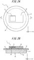
FIG. 2A is a front view of the communication apparatus inFIG. 1 ; -
FIG. 2B is a cross-section along the A-A line inFIG. 2A ; -
FIG. 3 is a block diagram schematically illustrating an example configuration of a communication apparatus according to an embodiment; -
FIG. 4 illustrates an example of transmission waves being reflected by a resonator; -
FIG. 5 is a graph illustrating the frequency characteristics of the phase difference between transmission waves and reflected waves; -
FIG. 6 is a graph illustrating the frequency characteristics of the intensity ratio of reflected waves to transmission waves; -
FIG. 7A illustrates an example of unit conductors, included in a resonator, that have a patch-like pattern; -
FIG. 7B illustrates an example of unit conductors, included in a resonator, that have a loop-like pattern; -
FIG. 7C illustrates an example of unit conductors, included in a resonator, that have a cross-like pattern; -
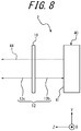
FIG. 8 illustrates reflection of transmission waves in a communication apparatus according to a Comparative Example; -
FIG. 9A is an example of a plan view of a communication apparatus according to an embodiment; -
FIG. 9B is a cross-section along the B-B line inFIG. 9A ; -
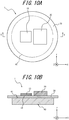
FIG. 10A is an example of a plan view of a communication apparatus according to an embodiment; -
FIG. 10B is a cross-section along the C-C line inFIG. 10A ; -
FIG. 11A is an example of a plan view of a communication apparatus according to an embodiment; -
FIG. 11B is a cross-section along the D-D line inFIG. 11A ; -
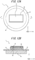
FIG. 12A is an example of a plan view of a communication apparatus according to an embodiment; and -
FIG. 12B is a cross-section along the E-E line inFIG. 12A . - When a communication apparatus 1 (see
FIG. 1 ) has a built-in flat battery 40 (seeFIG. 1 ), such as a button cell, thecommunication apparatus 1 may become larger than thebattery 40 as a result of an antenna 10 (seeFIG. 1 ) being arranged not to overlap thebattery 40. This makes it difficult to reduce thecommunication apparatus 1 in size. - The
communication apparatus 1 according to an embodiment includes anantenna 10, awireless module 20, and abattery 40, as illustrated inFIG. 1 and inFIGS. 2A and 2B . - The
communication apparatus 1 may include various structural members, such as a heat sink and a shield. Thebattery 40 may be included in a structural member. Thebattery 40 may, for example, be a button cell, a coin cell, or the like. Thebattery 40 may also be a rechargeable battery. Thebattery 40 in the example inFIG. 2B includes afirst surface 41, asecond surface 42, and aside surface 43. Thefirst surface 41 is positioned on the side in the positive direction of the Z-axis, and thesecond surface 42 is positioned on the side in the negative direction of the Z-axis. In other words, thefirst surface 41 and thesecond surface 42 are positioned on opposite sides of thebattery 40. Theside surface 43 is ring-shaped and is positioned between thefirst surface 41 and thesecond surface 42. The distance between thefirst surface 41 and thesecond surface 42 is also referred to as the height of thebattery 40. The area of thefirst surface 41 or thesecond surface 42 in plan view, when looking at thebattery 40 in plan view from the positive or negative direction of the Z-axis, is also referred to as the surface size of thebattery 40. The surface size of thebattery 40 may be the maximum dimension of thefirst surface 41 or thesecond surface 42. In the present embodiment, the surface size of thebattery 40 refers to whichever is larger in a comparison with the height of thebattery 40. - The
communication apparatus 1 may further include asubstrate 30. Thesubstrate 30 may have a shape that is the same as, or similar to, the shape of thefirst surface 41 of thebattery 40. Theantenna 10 and thewireless module 20 may be mounted on thesubstrate 30. - The
substrate 30 may be positioned to overlap thefirst surface 41 of thebattery 40 in plan view from the height direction of thebattery 40. Thesubstrate 30 may be positioned alongside thebattery 40 in the height direction of thebattery 40. Thebattery 40 may occupy a larger area in thecommunication apparatus 1 than other components of thecommunication apparatus 1 in plan view of thecommunication apparatus 1 from the Z-axis direction. The size of thecommunication apparatus 1 in plan view of thecommunication apparatus 1 from the Z-axis direction is also referred to as the surface size of thecommunication apparatus 1. The surface size of thebattery 40 may be considered to occupy the majority of the surface size of thecommunication apparatus 1. The surface size of thecommunication apparatus 1 can be reduced by positioning thesubstrate 30 to overlap thefirst surface 41 or thesecond surface 42, which define the surface size of thebattery 40, in the Z-axis direction. - The
antenna 10 emits electromagnetic waves on the basis of power that includes inputted current or voltage. Theantenna 10 may be included in thewireless module 20. Theantenna 10 may be separate from thewireless module 20. Theantenna 10 may be mounted on thesubstrate 30. Theantenna 10 may be mounted on thefirst surface 41 of thebattery 40. Theantenna 10 may be a conductor located on thesubstrate 30. Theantenna 10 may be a conductor located within thesubstrate 30. Theantenna 10 may be a chip antenna located on thesubstrate 30. Theantenna 10 may be a metal sheet antenna located on thesubstrate 30. - The
wireless module 20 supplies power including current or voltage to theantenna 10 to cause theantenna 10 to emit electromagnetic waves. Thewireless module 20 may be mounted on thesubstrate 30. Thewireless module 20 may be mounted on thefirst surface 41 of thebattery 40. - At least a portion of the surface of the
battery 40 may have the property of a conductor with high electric conductivity. The conductor may include a material whose electric conductivity decreases with an increase in temperature. The conductor may include a metal. The conductor may include gold, silver, copper, platinum, nickel, cadmium, lead, selenium, manganese, tin, vanadium, or lithium. The surface having conductive properties is also referred to as a conductor surface. In the present embodiment, thefirst surface 41 of thebattery 40 is assumed to be the conductor surface. Thefirst surface 41 is also referred to below as aconductor surface 41. Theconductor surface 41 is assumed to be grounded. The structural member including thebattery 40 can also be considered to have a conductor surface in at least a portion thereof. - The
antenna 10 may be positioned to overlap theconductor surface 41 in plan view from the Z-axis direction. Thecommunication apparatus 1 further includes aresonator 50 between theantenna 10 and theconductor surface 41. Theresonator 50 resonates in response to incidence of the electromagnetic waves. Theresonator 50 includes unit conductors 55 (seeFIGS. 7A, 7B, and 7C ) that reflect the electromagnetic waves and a conductor layer 56 (seeFIG. 4 ) on the side closer to thebattery 40 than theunit conductors 55. A conductor may be embedded in all or a portion of theresonator 50 as theconductor layer 56. Theresonator 50 can reflect the electromagnetic waves emitted from theantenna 10. The electromagnetic waves emitted from theantenna 10 are also referred to as transmission waves 12 (seeFIG. 4 ). When theresonator 50 reflects the transmission waves 12, the transmission waves 12 tend not to reach theconductor surface 41. When theconductor layer 56 is formed by a conductor embedded in all of theresonator 50, the transmission waves 12 are completely reflected by theresonator 50 and do not reach theconductor surface 41. - The
antenna 10 may be located on thesubstrate 30 or within thesubstrate 30. Theresonator 50 may be positioned closer to thebattery 40 than the conductor that forms theantenna 10. In plan view from the height direction of thebattery 40, theresonator 50 may be located in a wider range than the conductor that forms theantenna 10. In plan view from the height direction of thebattery 40, at least a portion of theresonator 50 may be located around theantenna 10. - The
resonator 50 may be provided in thewireless module 20. Theresonator 50 may be provided in thesubstrate 30. Theresonator 50 may be provided on thefirst surface 41 of thebattery 40. When oneresonator 50 is provided, theresonator 50 may be located in one of theantenna 10, thewireless module 20, thesubstrate 30, and thebattery 40. When a plurality ofresonators 50 is provided, theresonators 50 may be located in one or more of theantenna 10, thewireless module 20, thesubstrate 30, and thebattery 40. Theresonators 50 may be positioned to overlap each other in plan view from the Z-axis direction. Theresonators 50 may be positioned to overlap each other at least partially in plan view from the Z-axis direction. Theresonators 50 may be positioned not to overlap each other in plan view from the Z-axis direction. At least a portion of theresonators 50 may be positioned to overlap theantenna 10 in plan view from the Z-axis direction. Theresonators 50 may each have a different size in plan view from the Z-axis direction. - As illustrated in
FIG. 3 , thecommunication apparatus 1 may further include acontrol device 32, amemory device 34, and asensor 36. Thecontrol device 32, thememory device 34, and thesensor 36 may be mounted on thesubstrate 30. Thecontrol device 32 may be communicably connected to thewireless module 20, thememory device 34, and thesensor 36. Theantenna 10 may be electrically connected to thewireless module 20. Thebattery 40 can supply power to each component of thecommunication apparatus 1. - The
control device 32 generates a transmission signal to transmit from thecommunication apparatus 1. Thecontrol device 32 acquires measurement data from thesensor 36, for example. Thecontrol device 32 may generate the transmission signal on the basis of the measurement data. - The
control device 32 may, for example, be configured by a processor. Thecontrol device 32 may include one or more processors. The term "processor" encompasses universal processors that execute particular functions by reading particular programs and dedicated processors that are specialized for particular processing. The dedicated processor may include an application specific integrated circuit (ASIC). The processor may include a programmable logic device (PLD). The PLD may include a field-programmable gate array (FPGA). Thecontrol device 32 may be either a system-on-a-chip (SoC) or a system in a package (SiP) with one processor or a plurality of processors that work together. Thecontrol device 32 may store various information, programs for operating the components of thecommunication apparatus 1, and the like in thememory device 34. - The
memory device 34 may, for example, be a semiconductor memory. Thememory device 34 may function as a working memory of thecontrol device 32. Thememory device 34 may be included in thecontrol device 32. - The
sensor 36 may, for example, include a speed sensor, an acceleration sensor, a gyro sensor, a rotation angle sensor, an illuminance sensor, a geomagnetic sensor, a temperature sensor, a humidity sensor, a barometric pressure sensor, a global positioning system (GPS) signal receiver, or the like. - The
wireless module 20 may include a device capable of wireless communication by Bluetooth® (Bluetooth is a registered trademark in Japan, other countries, or both), a wireless local area network (LAN), or the like, for example. Thewireless module 20 may include a processor. Thewireless module 20 may include a digital signal processing (DSP) circuit. Thewireless module 20 may be configured to be capable of executing the functions of thecontrol device 32. Thewireless module 20 may include thecontrol device 32. Thewireless module 20 may include thememory device 34. - The
wireless module 20 may acquire the transmission signal from thecontrol device 32. Thewireless module 20 may generate the transmission signal. Thewireless module 20 can supply power based on the transmission signal to theantenna 10 and cause theantenna 10 to emit the transmission waves 12. Thewireless module 20 can supply power to theantenna 10 via voltage or current. The transmission waves 12 can be generated by modulating a carrier wave of a predetermined frequency in accordance with a signal. The transmission waves 12 may have a predetermined frequency band. The predetermined frequency band may include the frequency of the carrier wave. When the frequency of the carrier wave is approximately 2.5 GHz, the width of the predetermined frequency band may be 1 MHz, 20 MHz, or the like. The width of the predetermined frequency band may be a value sufficiently smaller than the frequency of the carrier wave. - As illustrated in
FIG. 4 , theantenna 10 can emit at least a portion of the transmission waves 12 in the positive direction of the Z-axis and the negative direction of the Z-axis. InFIG. 4 , the positive direction of the Z-axis is the direction from right to left. At least a portion of the transmission waves 12 can proceed in the negative direction of the Z-axis astransmission waves 12a. At least a portion of the transmission waves 12 proceeding in the negative direction of the Z-axis can proceed towards theconductor surface 41 of thebattery 40. The transmission waves 12a can be incident on theresonator 50. At least a portion of the transmission waves 12a can pass through theresonator 50 to be incident on theconductor surface 41 of thebattery 40 as transmission waves 12b. At least a portion of the transmission waves 12 can proceed in the positive direction of the Z-axis astransmission waves 12c. - The transmission waves 12a incident on the
resonator 50 can be reflected by theresonator 50 as reflected waves 52. The transmission waves 12a can cause theresonator 50 to resonate. The reflected waves 52 can be emitted from theresonator 50 by the resonance. In other words, theresonator 50 can reflect the transmission waves 12a as reflected waves 52. As illustrated inFIG. 5 , the phase difference between the transmission waves 12a and the reflected waves 52 can have a frequency characteristic. The horizontal axis ofFIG. 5 represents the frequency of the transmission waves 12a and the reflected waves 52. The vertical axis ofFIG. 5 represents the phase difference between the transmission waves 12a and the reflected waves 52. In the present disclosure, the phase difference when observing the surface on theantenna 10 side of theresonator 50 is simply referred to as the "phase difference". - The
resonator 50 has a resonance frequency. The resonance frequency is the frequency at which the phase difference between the transmission waves 12a and the reflected waves 52 becomes 0°. InFIG. 5 , the resonance frequency is represented as fr. - The
resonator 50 has a resonance frequency band set as a predetermined frequency range. The resonance frequency band is the frequency band between a first frequency and a second frequency. The first frequency is the frequency at which the phase difference between the transmission waves 12a and the reflected waves 52 is +90°. The second frequency is the frequency at which the phase difference between the transmission waves 12a and the reflected waves 52 is -90°. The resonance frequency band is also referred to as the resonance frequency range. The predetermined frequency range includes the resonance frequency. InFIG. 5 , the first frequency is represented as f1, and the second frequency as f2. - The phase difference between the transmission waves 12a and the reflected waves 52 can become 0° at the resonance frequency. The phase difference between the transmission waves 12a and the reflected waves 52 can approach 0° as the phase difference becomes closer to the resonance frequency. The phase difference between the transmission waves 12a and the reflected waves 52 can become 0°, or close to 0°, near the resonance frequency. The phase difference between the transmission waves 12a and the reflected waves 52 in a frequency band included in the resonance frequency band can be within a range of -90° to +90° at each frequency.
- The width of the resonance frequency band determined on the basis of the first and second frequencies may, for example, be 100 MHz or more when the resonance frequency is approximately 2.5 GHz.
- As illustrated in
FIG. 6 , the intensity ratio of the reflected waves 52 to the transmission waves 12a can have a frequency characteristic. The horizontal axis ofFIG. 6 represents the frequency of the transmission waves 12a and the reflected waves 52. The vertical axis ofFIG. 6 represents the intensity ratio of the reflected waves 52 to the transmission waves 12a. The intensity ratio is represented in units of decibels (dB). When the intensity ratio is 0 dB, the intensity of the reflected waves 52 is the same as the intensity of the transmission waves 12a. When the intensity ratio is less than 0 dB, the intensity of the reflected waves 52 is less than the intensity of the transmission waves 12a. InFIG. 6 , the resonance frequency is represented as fr. The first frequency is represented as f1, and the second frequency as f2. - The intensity ratio of the reflected waves 52 to the transmission waves 12a at the resonance frequency is smaller than the intensity ratio of the reflected waves 52 to the transmission waves 12a at other frequencies. The intensity ratio of the reflected waves 52 to the transmission waves 12a in the resonance frequency band is smaller than the intensity ratio of the reflected waves 52 to the transmission waves 12a at frequencies outside of the range of the resonance frequency band. The reduction in intensity ratio is caused by factors such as loss of current flowing at the time of resonance in the conductor included in the
resonator 50. - The
resonator 50 may include a plurality of theunit conductors 55. At least a portion of theunit conductors 55 can resonate at the resonance frequency of theresonator 50. At least a portion of theunit conductors 55 can resonate near the resonance frequency of theresonator 50. At least a portion of theunit conductors 55 can resonate near the resonance frequency (fr) of theresonator 50.FIGS. 7A, 7B, and 7C illustrate examples of the shape of theunit conductors 55 included in theresonator 50.FIG. 7A represents a patch-like pattern.FIG. 7B represents a loop-like pattern.FIG. 7C represents a cross-like pattern. Oneresonator 50 may includeunit conductors 55 with a plurality of shapes. Each of a plurality ofresonators 50 may includeunit conductors 55 with a different shape. - The size of the
unit conductors 55 can differ depending on the shape. The size of theunit conductors 55 may be a size that can resonate at the resonance frequency of theresonator 50 or at a frequency near the resonance frequency. A range of 1/10 to 1/20 of the wavelength of the transmission waves 12, for example, may be included in the sizes of theunit conductors 55. Theunit conductors 55 may, for example, be a conductive material. Theunit conductors 55 may, for example, be a thin film of metal. - The
unit conductors 55 may be arranged in a two-dimensional array in one layer or in each of a plurality of layers. Theunit conductors 55 may be arranged in a lattice in one layer or in each of a plurality of layers. The shape of the lattice is not limited to being square. Theunit conductors 55 may be arranged in a lattice in one layer or in each of a plurality of layers. Theunit conductors 55 may be aligned in a row in one layer or in each of a plurality of layers. Theunit conductors 55 included in oneresonator 50 may be aligned in a row in at least one layer and may be arranged in a lattice in at least one layer. Theunit conductors 55 may be arranged one-dimensionally. Theunit conductors 55 may be arranged two-dimensionally. Theunit conductors 55 may be arranged cyclically. The regions surrounded by dashed lines inFIGS. 7A, 7B, and 7C represent the pitch when theunit conductors 55 are arrayed periodically. Theunit conductors 55 may be arranged three-dimensionally. Oneresonator 50 may be a single-layer laminate in which theunit conductors 55 are arrayed two-dimensionally. - A structure in which an unlimited number of
unit conductors 55 are arrayed cyclically in two dimensions can function as a frequency selective surface (FSS). The FSS can function as an artificial magnetic conductor (AMC) by being combined with an electrically grounded portion. The AMC can reflect incident electromagnetic waves at substantially the same phase. - The
resonator 50 may be an FSS. When theresonator 50 is an FSS, theresonator 50 can function as an AMC by combination with theconductor surface 41 of thebattery 40. Theresonator 50 can function as an AMC by combination with a conductor included in thesubstrate 30. Theresonator 50 can function as an AMC by combination with a different grounded portion than theconductor surface 41. Theresonator 50 may include an electrically grounded portion. - The current flowing to the conductor included in the
resonator 50 is large when the resonance is intense. When a large current flows to the conductor, the energy loss can increase due to resistance loss in the conductor. In other words, intense resonance can decrease the intensity of the reflected waves 52. - The transmission waves 12b incident on the
conductor surface 41 of thebattery 40 are reflected by theconductor surface 41 and emitted as reflected waves 44. The reflected waves 44 proceed in the positive direction of the Z-axis. - The phase difference between the reflected waves 44 and the transmission waves 12b is approximately 180°.
- As the frequency of the transmission waves 12 is closer to the resonance frequency, more of the transmission waves 12a can be absorbed by the
resonator 50 and resonate. As the frequency of the transmission waves 12 is closer to the resonance frequency, the amount of the transmission waves 12b passing through theresonator 50 can decrease. In other words, when the transmission waves 12 have a frequency included in the resonance frequency band of theresonator 50, theresonator 50 can reduce the transmittance of the transmission waves 12. Theresonator 50 can prevent the transmission waves 12 that have a frequency included in the resonance frequency band from being directed towards theconductor surface 41 of thebattery 40. Thecommunication apparatus 1 may include aresonator 50 with one layer. Thecommunication apparatus 1 may include aresonator 50 with two or more layers. The transmittance of the transmission waves 12 can be reduced further by increasing the number of layers of theresonator 50. - When the distance between the
antenna 10 and theresonator 50 is short enough to be negligible relative to 1/4 of the wavelength of the transmission waves 12, the phase of the reflected waves 52 at theresonator 50 may be considered to be the same as the phase of the reflected waves 52 reaching theantenna 10. In this case, the phase difference between the transmission waves 12c proceeding in the positive direction of the Z-axis and the reflected waves 52 that reach theantenna 10 and continue in the same direction as the transmission waves 12c can be within a range of -90° to +90°. Consequently, the transmission waves 12c and the reflected waves 52 can proceed in the positive direction of the Z-axis without weakening each other. - When the frequency of the transmission waves 12 is 2.5 GHz, 1/4 of the wavelength of the transmission waves 12 is approximately 30 mm. The distance between the
antenna 10 and theresonator 50 may, for example, be 1 mm or less. In this case, the distance between theantenna 10 and theresonator 50 tends not to impede a reduction in size of thecommunication apparatus 1. - The transmission waves 12 can have a predetermined frequency band. When the resonance frequency band of the
resonator 50 includes a predetermined frequency band, the phase difference between the transmission waves 12a and the reflected waves 52 can be in a range of -90° to +90° at each frequency component of the transmission waves 12. The transmission waves 12 in this case can proceed in the positive direction of the Z-axis without being weakened by the reflected waves 52. - At least a portion of the frequency components of the transmission waves 12 can resonate at the
resonator 50 when the resonance frequency of theresonator 50 is included in a predetermined frequency band. The width of the resonance frequency band tends to be larger than the width of the predetermined frequency band of the transmission waves 12. When the resonance frequency band is wider than the width of the predetermined frequency band of the transmission waves 12, the phase difference between the transmission waves 12a and the reflected waves 52 can be in a range of -90° to +90° at each frequency component of the transmission waves 12. The transmission waves 12 in this case can proceed in the positive direction of the Z-axis without being weakened by the reflected waves 52. - As illustrated in
FIG. 8 , a communication apparatus 2 according to a Comparative Example does not include theresonator 50. No transmission waves 12a are incident on theresonator 50. The transmission waves 12b proceeding in the negative direction of the Z-axis are incident on theconductor surface 41 of thebattery 40. The transmission waves 12a are reflected by theconductor surface 41 and proceed in the positive direction of the Z-axis as reflected waves 44. The phase difference between the reflected waves 44 and thetransmission waves 12a is approximately 180°. InFIG. 8 , the positive direction of the Z-axis is the direction from right to left. - When the distance between the
antenna 10 and theconductor surface 41 is short enough to be negligible relative to 1/4 of the wavelength of the transmission waves 12, the phase of the reflected waves 44 reflected by theconductor surface 41 may be considered to be the same as the phase of the reflected waves 44 reaching theantenna 10. In this case, the phase difference between the transmission waves 12c proceeding in the positive direction of the Z-axis and the reflected waves 44 that reach theantenna 10 and continue in the same direction as the transmission waves 12c can be nearly 180°. Consequently, the transmission waves 12c and the reflected waves 44 weaken each other. The intensity of the transmission waves 12 emitted from theantenna 10 may weaken as a result of the transmission waves 12c and the reflected waves 44 weakening each other. - The distance that the electromagnetic waves travel from the
antenna 10 to theconductor surface 41 and back is 1/2 of the wavelength of the transmission waves 12 when the distance between theantenna 10 and theconductor surface 41 is 1/4 of the wavelength. In this case, the phase shifts by 180° while the electromagnetic waves travel from theantenna 10 to theconductor surface 41 and back. This 180° shift in phase due to reflection at theconductor surface 41 causes the transmission waves 12c and the reflected waves 44 to intensify each other. In other words, even when thecommunication apparatus 1 does not include theresonator 50, the transmission waves 12 from theantenna 10 can be intensified by setting the distance between theantenna 10 and theconductor surface 41 to 1/4 the wavelength of the transmission waves 12. For example, 1/4 of the wavelength of the transmission waves 12 is approximately 30 mm when the frequency of the transmission waves 12 is 2.5 GHz. The height of thebattery 40 is often less than 5 mm when thebattery 40 is a button cell. - The size of the communication apparatus 2 in the Z-axis direction may become larger than the height of the
battery 40 when the distance between theantenna 10 and theconductor surface 41 is designed so that the transmission waves 12c and the reflected waves 44 intensify each other. When theresonator 50 is not included, the grounding state of theconductor surface 41 can easily change as a result of a human body or the like approaching or coming into contact with the communication apparatus 2. The phase of the reflected waves 44 can easily change in response to a change in the grounding state of theconductor surface 41. Consequently, the intensity of the transmission waves 12 tends to become unstable. - In the communication apparatus 2 according to the Comparative Example, which does not include the
resonator 50, it is difficult both to intensify the transmission waves 12 from theantenna 10 and to reduce the communication apparatus 2 in size. Consequently, the intensity of the transmission waves 12 tends to become unstable in the communication apparatus according to the Comparative Example. - In the communication apparatus 2 according to the Comparative Example, the effect of the
conductor surface 41 on the transmission waves 12 can be reduced by disposing an insulating layer between theantenna 10 and theconductor surface 41. The insulating layer tends to be thicker than theresonator 50. In other words, it is also difficult to reduce the communication apparatus 2 according to the Comparative Example in size when providing an insulating layer in the communication apparatus 2. - As illustrated in
FIGS. 9A and 9B , thecommunication apparatus 1 according to an embodiment may be configured so that theantenna 10 and theconductor surface 41 of thebattery 40 do not overlap. This configuration can attenuate the reflected waves 44 produced by reflection of the transmission waves 12 emitted from theantenna 10, regardless of whether thecommunication apparatus 1 includes theresonator 50. The intensity of the transmission waves 12 is then less likely to decrease, because the transmission waves 12 tend not to be weakened by the reflected waves 44. - Even when the
conductor surface 41 and theantenna 10 included in thecommunication apparatus 1 are shifted away from each other, theantenna 10 may overlap a conductor positioned outside of thecommunication apparatus 1. By including theresonator 50, thecommunication apparatus 1 can stabilize fluctuation in the intensity due to conductors located nearby. - As illustrated in
FIGS. 10A and 10B , theantenna 10 and thewireless module 20 may be mounted as separate components in thecommunication apparatus 1 according to an embodiment. Theantenna 10 and thewireless module 20 may be mounted on thesubstrate 30. Theresonator 50 may be provided on the surface of theantenna 10 facing thebattery 40. Theresonator 50 may have an area equivalent to the area of theantenna 10 or may have a larger area. Theresonator 50 may be provided in thesubstrate 30. Theresonator 50 may be provided on thefirst surface 41 of thebattery 40. - Provision of the
antenna 10 and thewireless module 20 as separate components can increase the degree of freedom for arrangement of theantenna 10. - As illustrated in
FIGS. 11A and 11B , theantenna 10 may be included in thesubstrate 30 in thecommunication apparatus 1 according to an embodiment. Theresonator 50 may be provided on the surface of thesubstrate 30 on thebattery 40 side. Theresonator 50 may have an area equivalent to the area of theantenna 10 or may have a larger area. Theresonator 50 may be provided on thefirst surface 41 of thebattery 40. - Inclusion of the
antenna 10 in thesubstrate 30 can increase the area of theantenna 10. - As illustrated in
FIGS. 12A and 12B , theantenna 10 and thewireless module 20 may be stacked in thecommunication apparatus 1 according to an embodiment. Theresonator 50 may be provided on the surface of theantenna 10 on thebattery 40 side. Theresonator 50 may have an area equivalent to the area of theantenna 10 or may have a larger area. Theresonator 50 may be provided in thewireless module 20 or thesubstrate 30. Theresonator 50 may be provided on thefirst surface 41 of thebattery 40. - Stacking the
antenna 10 on thewireless module 20 can increase the area of theantenna 10. - Configurations according to the present disclosure are not limited to the above embodiments, and a variety of modifications and changes are possible. For example, the functions and the like included in the various components may be reordered in any logically consistent way. Furthermore, components may be combined into one or divided.
- The drawings illustrating configurations according to the present disclosure are merely schematic. The dimensional ratios and the like in the drawings do not necessarily match the actual dimensions.
- The references to "first", "second", and the like in the present disclosure are identifiers for distinguishing between the corresponding elements. The numbers of elements distinguished by references to "first", "second", and the like in the present disclosure may be switched. For example, the identifiers "first" and "second" of the first frequency and the second frequency may be switched. Identifiers are switched simultaneously, and the elements are still distinguished between after identifiers are switched. The identifiers may be removed. Elements from which the identifiers are removed are distinguished by their reference sign. Identifiers in the present disclosure, such as "first" and "second", may not be used in isolation as an interpretation of the order of elements or as the basis for the existence of the identifier with a lower number.
- In the present disclosure, the X-axis, Y-axis, and Z-axis are provided for the sake of explanation and may be interchanged. Configurations according to the present disclosure have been described using an orthogonal coordinate system constituted by the X-axis, Y-axis, and Z-axis. The positional relationships between elements according to the present disclosure are not limited to orthogonal relationships.
-
- 1, 2
- Communication apparatus
- 10
- Antenna
- 12
- Transmission waves
- 20
- Wireless module
- 30
- Substrate
- 32
- Control device
- 34
- Memory device
- 40
- Battery
- 41
- First surface (conductor surface)
- 42
- Second surface
- 43
- Side surface
- 44
- Reflected waves
- 50
- Resonator
- 52
- Reflected waves
- 55
- Unit conductor
- 56
- Conductor layer
Claims (3)
- A communication apparatus comprising:an antenna;a wireless module configured to supply power to the antenna to cause the antenna to emit electromagnetic waves having a predetermined frequency band;at least one structural member having a conductor surface on at least a portion of the at least one structural member; andat least one resonator comprising a plurality of unit conductors, and having a resonance frequency band that includes a resonance frequency, the at least one resonator positioned between the conductor surface and the antenna; andwherein the predetermined frequency band is included in the resonance frequency band.
- The communication apparatus of claim 1, wherein
the resonance frequency is included in the predetermined frequency band. - The communication apparatus of claim 1 or 2, wherein
a plurality of the resonators is positioned between the antenna and the conductor surface.
Applications Claiming Priority (2)
| Application Number | Priority Date | Filing Date | Title |
|---|---|---|---|
| JP2016208177 | 2016-10-24 | ||
| PCT/JP2017/038343 WO2018079543A1 (en) | 2016-10-24 | 2017-10-24 | Communication device |
Publications (2)
| Publication Number | Publication Date |
|---|---|
| EP3531507A1 true EP3531507A1 (en) | 2019-08-28 |
| EP3531507A4 EP3531507A4 (en) | 2020-05-27 |
Family
ID=62024128
Family Applications (1)
| Application Number | Title | Priority Date | Filing Date |
|---|---|---|---|
| EP17864406.8A Withdrawn EP3531507A4 (en) | 2016-10-24 | 2017-10-24 | Communication device |
Country Status (4)
| Country | Link |
|---|---|
| US (1) | US20190273304A1 (en) |
| EP (1) | EP3531507A4 (en) |
| JP (1) | JPWO2018079543A1 (en) |
| WO (1) | WO2018079543A1 (en) |
Families Citing this family (4)
| Publication number | Priority date | Publication date | Assignee | Title |
|---|---|---|---|---|
| EP3506656B1 (en) * | 2017-12-29 | 2023-02-22 | GN Hearing A/S | A hearing instrument comprising a parasitic battery antenna element |
| JP7217429B2 (en) * | 2019-03-29 | 2023-02-03 | パナソニックIpマネジメント株式会社 | antenna device |
| JP7449746B2 (en) * | 2020-03-27 | 2024-03-14 | 京セラ株式会社 | Antenna, wireless communication module, baggage receiving device and baggage receiving system |
| JP7817052B2 (en) * | 2021-04-28 | 2026-02-18 | キヤノンメディカルシステムズ株式会社 | Periodic structure and magnetic resonance imaging device |
Family Cites Families (9)
| Publication number | Priority date | Publication date | Assignee | Title |
|---|---|---|---|---|
| JP2007060607A (en) * | 2005-07-25 | 2007-03-08 | Nec Tokin Corp | High impedance sheet |
| US7679577B2 (en) * | 2006-06-09 | 2010-03-16 | Sony Ericsson Mobile Communications Ab | Use of AMC materials in relation to antennas of a portable communication device |
| JP5217494B2 (en) * | 2007-05-08 | 2013-06-19 | 旭硝子株式会社 | Artificial medium, method for manufacturing the same, and antenna device |
| JP5470155B2 (en) * | 2010-05-17 | 2014-04-16 | 日本電信電話株式会社 | Antenna device |
| JP6002540B2 (en) * | 2012-10-25 | 2016-10-05 | 日本電信電話株式会社 | Antenna device |
| JP2015046846A (en) * | 2013-08-29 | 2015-03-12 | 日本電信電話株式会社 | ANTENNA DEVICE DESIGNING METHOD AND ANTENNA DEVICE |
| KR102139217B1 (en) * | 2014-09-25 | 2020-07-29 | 삼성전자주식회사 | Antenna device |
| JPWO2018168699A1 (en) * | 2017-03-14 | 2020-01-16 | 日本電気株式会社 | Heat dissipation mechanism and wireless communication device |
| US20190097299A1 (en) * | 2017-09-22 | 2019-03-28 | Kymeta Corporation | Integrated transceiver for antenna systems |
-
2017
- 2017-10-24 WO PCT/JP2017/038343 patent/WO2018079543A1/en not_active Ceased
- 2017-10-24 EP EP17864406.8A patent/EP3531507A4/en not_active Withdrawn
- 2017-10-24 US US16/344,361 patent/US20190273304A1/en not_active Abandoned
- 2017-10-24 JP JP2018547684A patent/JPWO2018079543A1/en active Pending
Also Published As
| Publication number | Publication date |
|---|---|
| JPWO2018079543A1 (en) | 2019-08-08 |
| EP3531507A4 (en) | 2020-05-27 |
| WO2018079543A1 (en) | 2018-05-03 |
| US20190273304A1 (en) | 2019-09-05 |
Similar Documents
| Publication | Publication Date | Title |
|---|---|---|
| EP3531507A1 (en) | Communication device | |
| JP6347424B2 (en) | Wireless module | |
| WO2016112838A1 (en) | Multi-band antenna on the surface of wireless communication devices | |
| CN115275557A (en) | Electronic device with folded antenna module | |
| JP6132692B2 (en) | Antenna device | |
| CN110165363A (en) | Omnidirectional antenna for cylinder-shaped body | |
| US11870144B2 (en) | Antenna, wireless communication module, and wireless communication device | |
| KR102742799B1 (en) | Electronic devices having compact ultra-wideband antenna modules | |
| JPWO2019026913A1 (en) | Multi-axis antenna, wireless communication module, and wireless communication device | |
| JPWO2016159369A1 (en) | Multiband antenna and wireless communication device | |
| US11843174B2 (en) | Antenna element, array antenna, communication unit, mobile body, and base station | |
| JP2015095813A5 (en) | ||
| JP2017098782A (en) | Antenna element | |
| JP7072724B2 (en) | Antennas, wireless communication modules and wireless communication devices | |
| JP7122389B2 (en) | Antennas, array antennas, wireless communication modules, and wireless communication equipment | |
| CN110957586A (en) | An electronic device integrating a new millimeter-wave array antenna | |
| Loizou et al. | Design and analysis of a dual-band inverted-F antenna with orthogonal frequency-controlled radiation planes | |
| JP2021141416A (en) | antenna | |
| JP6926174B2 (en) | Antennas, wireless communication modules and wireless communication devices | |
| WO2020175659A1 (en) | Band-type article | |
| US12160055B2 (en) | Antenna, wireless communication module, and wireless communication device | |
| JP7483456B2 (en) | Communication device, communication system and control method | |
| JP7137012B2 (en) | Antennas, wireless communication modules and wireless communication equipment | |
| US20250087868A1 (en) | Electronic Device with Folded Antenna Module | |
| CN112311912B (en) | Shell assembly and manufacturing method thereof, antenna assembly and electronic equipment |
Legal Events
| Date | Code | Title | Description |
|---|---|---|---|
| PUAI | Public reference made under article 153(3) epc to a published international application that has entered the european phase |
Free format text: ORIGINAL CODE: 0009012 |
|
| STAA | Information on the status of an ep patent application or granted ep patent |
Free format text: STATUS: REQUEST FOR EXAMINATION WAS MADE |
|
| 17P | Request for examination filed |
Effective date: 20190424 |
|
| AK | Designated contracting states |
Kind code of ref document: A1 Designated state(s): AL AT BE BG CH CY CZ DE DK EE ES FI FR GB GR HR HU IE IS IT LI LT LU LV MC MK MT NL NO PL PT RO RS SE SI SK SM TR |
|
| AX | Request for extension of the european patent |
Extension state: BA ME |
|
| DAV | Request for validation of the european patent (deleted) | ||
| DAX | Request for extension of the european patent (deleted) | ||
| A4 | Supplementary search report drawn up and despatched |
Effective date: 20200428 |
|
| RIC1 | Information provided on ipc code assigned before grant |
Ipc: H01Q 1/52 20060101ALI20200421BHEP Ipc: H01Q 1/24 20060101ALI20200421BHEP Ipc: H04B 1/525 20150101ALI20200421BHEP Ipc: H01Q 15/00 20060101ALI20200421BHEP Ipc: H01Q 15/14 20060101AFI20200421BHEP |
|
| STAA | Information on the status of an ep patent application or granted ep patent |
Free format text: STATUS: THE APPLICATION IS DEEMED TO BE WITHDRAWN |
|
| 18D | Application deemed to be withdrawn |
Effective date: 20201126 |