EP3531255A1 - Touch panel device - Google Patents
Touch panel device Download PDFInfo
- Publication number
- EP3531255A1 EP3531255A1 EP17861960.7A EP17861960A EP3531255A1 EP 3531255 A1 EP3531255 A1 EP 3531255A1 EP 17861960 A EP17861960 A EP 17861960A EP 3531255 A1 EP3531255 A1 EP 3531255A1
- Authority
- EP
- European Patent Office
- Prior art keywords
- electrode
- pressing force
- voltage
- points
- cpu
- Prior art date
- Legal status (The legal status is an assumption and is not a legal conclusion. Google has not performed a legal analysis and makes no representation as to the accuracy of the status listed.)
- Granted
Links
Images



Classifications
-
- G—PHYSICS
- G06—COMPUTING OR CALCULATING; COUNTING
- G06F—ELECTRIC DIGITAL DATA PROCESSING
- G06F3/00—Input arrangements for transferring data to be processed into a form capable of being handled by the computer; Output arrangements for transferring data from processing unit to output unit, e.g. interface arrangements
- G06F3/01—Input arrangements or combined input and output arrangements for interaction between user and computer
- G06F3/03—Arrangements for converting the position or the displacement of a member into a coded form
- G06F3/041—Digitisers, e.g. for touch screens or touch pads, characterised by the transducing means
- G06F3/045—Digitisers, e.g. for touch screens or touch pads, characterised by the transducing means using resistive elements, e.g. a single continuous surface or two parallel surfaces put in contact
-
- G—PHYSICS
- G06—COMPUTING OR CALCULATING; COUNTING
- G06F—ELECTRIC DIGITAL DATA PROCESSING
- G06F3/00—Input arrangements for transferring data to be processed into a form capable of being handled by the computer; Output arrangements for transferring data from processing unit to output unit, e.g. interface arrangements
- G06F3/01—Input arrangements or combined input and output arrangements for interaction between user and computer
- G06F3/03—Arrangements for converting the position or the displacement of a member into a coded form
- G06F3/041—Digitisers, e.g. for touch screens or touch pads, characterised by the transducing means
- G06F3/0414—Digitisers, e.g. for touch screens or touch pads, characterised by the transducing means using force sensing means to determine a position
-
- G—PHYSICS
- G06—COMPUTING OR CALCULATING; COUNTING
- G06F—ELECTRIC DIGITAL DATA PROCESSING
- G06F3/00—Input arrangements for transferring data to be processed into a form capable of being handled by the computer; Output arrangements for transferring data from processing unit to output unit, e.g. interface arrangements
- G06F3/01—Input arrangements or combined input and output arrangements for interaction between user and computer
- G06F3/03—Arrangements for converting the position or the displacement of a member into a coded form
- G06F3/041—Digitisers, e.g. for touch screens or touch pads, characterised by the transducing means
- G06F3/0416—Control or interface arrangements specially adapted for digitisers
-
- G—PHYSICS
- G06—COMPUTING OR CALCULATING; COUNTING
- G06F—ELECTRIC DIGITAL DATA PROCESSING
- G06F2203/00—Indexing scheme relating to G06F3/00 - G06F3/048
- G06F2203/041—Indexing scheme relating to G06F3/041 - G06F3/045
- G06F2203/04104—Multi-touch detection in digitiser, i.e. details about the simultaneous detection of a plurality of touching locations, e.g. multiple fingers or pen and finger
Definitions
- the present invention relates to a touch panel device.
- the above-mentioned Document D1 discloses a method of detecting the pressing force when a single point of the touch panel is pressed, but does not disclose a method of detecting pressing forces of two points when the two points of the touch panel are pressed at the same time.
- the single sensor cannot detect which of the two points of the touch panel is pressed strongly.
- the manufacturing cost of the touch panel increases and a complex control processing is required to control the plurality of sensors.
- a touch panel device characterized by comprising: a first resistive film in which a first electrode and a second electrode are provided at both ends in a first direction; a second resistive film in which a third electrode and a fourth electrode are provided at both ends in a second direction perpendicular to the first direction; a plurality of switches that are connected to the first to the fourth electrodes, respectively; a first measurement means that controls the switches so as to apply a voltage to the second electrode and ground the third electrode, and measures a voltage difference between the first electrode and the fourth electrode as a first pressing force; a second measurement means that controls the switches so as to apply a voltage to the first electrode and ground the fourth electrode, and measures a voltage difference between the second electrode and the third electrode as a second pressing force; and an association means that associates the first pressing force and the second pressing force with coordinates of two contact points, respectively, and outputs a result of the association to an external device.
- FIG. 1A is a diagram illustrating a touch panel device according to a present embodiment.
- a touch panel device 100 includes: switches SW1 to SW9; resistances R, Rx1 and Ry1; resistive films 10 and 20; a control unit 30; and an input/output unit 36, as illustrated in FIG. 1A .
- the resistive film 10 is an upper resistive film
- the resistive film 20 is a lower resistive film.
- the resistive films 10 and 20 are arranged opposite to each other, and superposed on a display device such as a liquid crystal display (not illustrated), for example.
- An XH electrode 12 (i.e., a first electrode) is provided on one side of the resistive film 10 (i.e., a first resistive film), and an XL electrode 14 (i.e., a second electrode) opposite to the XH electrode 12 is provided on another one side of the resistive film 10.
- a YH electrode 22 i.e., a third electrode
- a YL electrode 24 i.e., a fourth electrode
- the resistive films 10 and 20 are transparent conductive films made of ITO (Indium Tin Oxide), for example.
- the resistive films 10 and 20 are formed by the same material, for example, and electrical resistance is substantially uniformly distributed.
- the XH electrode 12, the XL electrode 14, the YH electrode 22 and the YL electrode 24 are made of metal such as copper or aluminum, for example.
- the switches SW1 to SW9 are made of transistors, respectively. A base of the transistor of each switch is connected to the control unit 30. Each emitter of the switches SW1, SW4 and SW8 is connected to a supply voltage Vcc. An emitter of the switch SW2 is connected to the supply voltage Vcc via the resistance Rx1. An emitter of the switch SW5 is connected to the supply voltage Vcc via the resistance Ry1. Each emitter of the switches SW3, SW6, SW7 and SW9 is grounded.
- the supply voltage Vcc is 5V, for example.
- the XH electrode 12 is connected to collectors of the switches SW1 and SW2, and a collector of the switch SW7 via the resistance R.
- the XL electrode 14 is connected to collectors of the switches SW3 and SW8.
- the YH electrode 22 is connected to collectors of the switches SW4, SW5 and SW9.
- the YL electrode 24 is connected to a collector of the switch SW6.
- the control unit 30 is connected to a computer 40 as an external device via the input/output unit 36. Data on the touch input acquired by the control unit 30 is transmitted to the computer 40 via the input/output unit 36.
- the control unit 30 includes a Central Processing Unit (CPU) 31, an AD converter 32 and a memory 33.
- the CPU 31 serves as a first measurement means, a second measurement means, an association means, a comparison means and a detection means.
- the AD converter 32 includes voltage detection units ADX1, ADX2, ADY1 and ADY2.
- the voltage detection unit ADX1 is connected to the XH electrode 12, and the voltage detection unit ADX2 is connected to the XL electrode 14.
- the voltage detection unit ADY1 is connected to the YH electrode 22, and the voltage detection unit ADY2 is connected to the YL electrode 24.
- the memory 33 stores voltages detected by the voltage detection units ADX1, ADX2, ADY1 and ADY2, data necessary for coordinate detection, and so on.
- An electrical resistance of the resistance Rx1 is substantially the same as the electrical resistance of the resistive film 10 between the XH electrode 12 and the XL electrode 14.
- the electrical resistance of the resistance Ry1 is substantially the same as the electrical resistance of the resistive film 20 between the YH electrode 22 and the YL electrode 24.
- FIG. 1B is a functional block diagram illustrating functions of the CPU 31.
- the CPU 31 serves as an application unit 34 and a detection unit 35.
- the application unit 34 applies voltages to the switches SW1 to SW9 to control on/off of the switches SW1 to SW9, thereby controlling a voltage to be applied to each electrode.
- the detection unit 35 acquires the voltages detected by the voltage detection units ADX1, ADX2, ADY1 and ADY2, and detects whether the touch input is single point pressing or two point pressing, coordinates of a middle point in case of the two point pressing, a distance between the two points, a direction of a line connecting the two points, a pressing force of at least one contact point, and coordinates of the contact point, based on the acquired voltages.
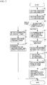
- FIG. 2 is a flowchart illustrating a detection process of the contact point to be executed by the CPU 31.
- the CPU 31 detects a voltage in the X-axis direction (step S1). Specifically, the CPU 31 turns on the switches SW2 and SW3, turns off other switches excluding them, and the voltage detection unit ADX1 measures the voltage. In this state, since the voltage of Vcc is applied to the XH electrode 12 through the resistance Rx1 and the XL electrode 14 is grounded, an electric potential distribution occurs in the X-axis direction of the resistive film 10. In this state, the voltage is measured by the voltage detection unit ADX1, and the measured voltage is stored into the memory 33.
- the voltage to be detected by the voltage detection unit ADX1 is a value partially divided by the resistance Rx1 and a resistance component between the XH electrode 12 and the XL electrode 14.
- the CPU 31 detects a voltage in the Y-axis direction (step S2). Specifically, the CPU 31 turns on the switches SW5 and SW6, turns off other switches excluding them, and the voltage detection unit ADY1 measures the voltage. In this state, since the voltage of Vcc is applied to the YH electrode 22 through the resistance Ry1 and the YL electrode 24 is grounded, an electric potential distribution occurs in the Y-axis direction of the resistive film 20. In this state, the voltage is measured by the voltage detection unit ADY1, and the measured voltage is stored into the memory 33.
- the voltage to be detected by the voltage detection unit ADY1 is a value partially divided by the resistance Ry1 and a resistance component between the YH electrode 22 and the YL electrode 24.
- the CPU 31 determines whether the contact point is a single point or two points (step S3). Specifically, the CPU 31 determines whether the voltage measured by the voltage detection unit ADX1 in step S1 and the voltage measured by the voltage detection unit ADY1 in step S2 are Vcc/2 or less than Vcc/2. When the voltages measured by the voltage detection units ADX1 and ADY1 are Vcc/2, the CPU 31 determines that the contact point is the single point. On the other hand, when the voltages measured by the voltage detection units ADX1 and ADY1 are less than Vcc/2, the CPU 31 determines that the contact point is the two points.
- the resistance value between the XH electrode 12 and the XL electrode 14 is a total value of resistance components R1 and R2, and the total value is substantially equal to a value of the resistance Rx1. Therefore, the voltage to be detected by the voltage detection unit ADX1 becomes Vcc/2.
- the resistance value between the YH electrode 22 and the YL electrode 24 is a total value of resistance components R3 and R4, and the total value is substantially equal to a value of the resistance Ry1. Therefore, the voltage to be detected by the voltage detection unit ADY1 becomes Vcc/2.
- the resistance value between the XH electrode 12 and the XL electrode 14 is a synthetic resistance value of a resistance component R11, a resistance component in which a resistance component R12 and a resistance component R22 are connected in parallel, and a resistance component R13. Since a parallel resistance component of the resistance components R12 and R22 is included, the synthetic resistance value of FIG. 3C becomes lower than the resistance Rx1. Therefore, the voltage to be detected by the voltage detection unit ADX1 becomes lower than Vcc/2.
- the resistance value between the YH electrode 22 and the YL electrode 24 is a synthetic resistance value of a resistance component R21, a resistance component in which a resistance component R12 and a resistance component R22 are connected in parallel, and a resistance component R23. Therefore, the synthetic resistance value of FIG. 3D becomes lower than the resistance Ry1. Therefore, the voltage to be detected by the voltage detection unit ADY1 becomes lower than Vcc/2.
- step S4 when it is determined in step S3 that the contact point is the single point, the CPU 31 detects the coordinates of the contact point by a normal position detection method (step S4).
- the CPU 31 turns on the switches SW1 and SW3, turns off other switches excluding them, and detects an X-coordinate of the contact point based on the voltage measured by the voltage detection unit ADX1.
- the CPU 31 calculates a distance in the X-axis direction from the XH electrode 12 to the contact point by multiplying the voltage measured by the voltage detection unit ADX1 by a ratio of a distance between the XH electrode 12 and the XL electrode 14 to an electric potential difference between the XH electrode 12 and the XL electrode 14, for example.
- the CPU 31 turns on the switches SW4 and SW6, turns off other switches excluding them, and detects a Y-coordinate of the contact point based on the voltage measured by the voltage detection unit ADY1.
- the CPU 31 calculates a distance in the Y-axis direction from the YH electrode 22 to the contact point by multiplying the voltage measured by the voltage detection unit ADY1 by a ratio of a distance between the YH electrode 22 and the YL electrode 24 to an electric potential difference between the YH electrode 22 and the YL electrode 24.
- the CPU 31 turns on the switches SW8 and SW9, turns off other switches excluding them, detects an electric potential difference between the voltage measured by the voltage detection unit ADX1 and the voltage measured by the voltage detection unit ADY2, i.e., a voltage applied to a contact resistance of the contact point, and stores the detected potential difference into the memory 33 as the pressing force (step S5).
- the CPU 31 associates the coordinates of the contact point detected in step S4 and the electric potential difference detected in step S5 to create touch data and output the touch data to the computer 40 via the input/output unit 36 (step S6).
- the present process is terminated.
- step S3 when it is detected in step S3 that the contact point is the two points, the CPU 31 determines whether the inclination of the line connecting the two points is parallel to the X-axis or Y-axis direction, or a diagonal direction (step S7).
- the CPU 31 turns on the switches SW2 and SW3 and turns off other switches excluding them to generate an electrical potential distribution in the X-axis direction of the resistive film 10, and the voltage detection unit ADX1 measures the voltage.
- the CPU 31 stores the voltage measured by the voltage detection unit ADX1 into the memory 33 as an initial voltage ⁇ 1.
- the CPU 31 turns on the switches SW5 and SW6 and turns off other switches excluding them to generate an electrical potential distribution in the Y-axis direction of the resistive film 20, and the voltage detection unit ADY1 measures the voltage.
- the CPU 31 stores the voltage measured by the voltage detection unit ADY1 into the memory 33 as an initial voltage ⁇ 2.
- Such a setting of the initial voltage can be carried out at appropriate timing such as when the device is began to use or is manufactured, for example.
- the CPU 31 determines whether the line connecting the two points is parallel to the X-axis or Y-axis direction, or the diagonal direction with respect to the X-axis direction or Y-axis direction, by comparing the voltages measure in steps S1 and S2 with the stored initial voltages ⁇ 1 and ⁇ 2.
- the CPU 31 determines that the line connecting the two points is parallel to the X-axis direction.
- the CPU 31 determines that the line connecting the two points is parallel to the Y-axis direction.
- the CPU 31 determines that the line connecting the two points is the diagonal direction.
- the CPU 31 turns on the switches SW1 and SW3 and turns off other switches excluding them to generate an electrical potential distribution in the X-axis direction of the resistive film 10, and the voltage detection units ADY1 and ADY 2 measure the voltages.
- the CPU 31 determines that the inclination of the line connecting the two points is upward to the right.
- the CPU 31 determines that the inclination of the line connecting the two points is upward to the left.
- the CPU 31 calculates midpoint coordinates of the two points (step S8). Specifically, the CPU31 turns on the switches SW1 and SW3 and turns off other switch excluding them to generate the electrical potential distribution in the X-axis direction of the resistive film 10, and the voltage detection units ADY1 and ADY2 measure the voltages. The CPU 31 acquires a voltage in the X-axis direction corresponding to the midpoint of the two points by calculating an average value of the voltage detected by the voltage detection unit ADY2 and the voltage detected by the voltage detection unit ADY1, and acquires an X-coordinate of the midpoint based on the acquired voltage in the X-axis direction.
- the CPU 31 acquires a distance in the X-axis direction from the XH electrode 12 by multiplying the above-mentioned calculated average value by a ratio of the distance between the XH electrode 12 and the XL electrode 14 to the electric potential difference between the voltage detected by the voltage detection unit ADY1 and the voltage detected by the voltage detection unit ADY2.
- the CPU31 turns on the switches SW4 and SW6 and turns off other switch excluding them to generate the electrical potential distribution in the Y-axis direction of the resistive film 20, and the voltage detection units ADX1 and ADX2 measure the voltages.
- the CPU 31 acquires a voltage in the Y-axis direction corresponding to the midpoint of the two points by calculating an average value of the voltage detected by the voltage detection unit ADX1 and the voltage detected by the voltage detection unit ADX2, and acquires a Y-coordinate of the midpoint based on the acquired voltage in the Y-axis direction.
- the CPU 31 acquires a distance in the Y-axis direction from the YH electrode 22 by multiplying the above-mentioned calculated average value by a ratio of the distance between the YH electrode 22 and the YL electrode 24 to the electric potential difference between the voltage detected by the voltage detection unit ADX1 and the voltage detected by the voltage detection unit ADX2.
- the CPU 31 calculates the distance between the two points (step S9). Specifically, the CPU 31 calculates the distance between the two points in contact with the touch panel device 100, based on the voltages measured in steps S1 and S2.
- FIG. 4 is a diagram illustrating distance calculation data indicating a relationship between the distance between the two points in the X-axis direction, and the voltage to be detected by the voltage detection unit ADX1.
- the distance calculation data is stored into the memory 33.
- the value of the voltage to be detected by the voltage detection unit ADX1 is decreased.
- relationships between the distance between the two points and the voltage to be detected by the voltage detection unit ADX1 are different from each other.
- the CPU 31 can select the relationship between the distance between the two points and the voltage detected by the voltage detection unit ADX1 as illustrated in FIG. 4 , in accordance with a positional relationship of the two points detected in step S6, i.e., the inclination of the line connecting the two points, and can acquire the distance between the two points in the X-axis direction based on the selected relationship.
- the CPU 31 can calculate the distance between the two points in the X-direction based on a curve indicated by a line 41a in FIG. 4 and the voltage detected by the voltage detection unit ADX1.
- the CPU 31 can calculate the distance between the two points in the X-direction based on a curve indicated by a line 41b in FIG. 4 and the voltage detected by the voltage detection unit ADX1.
- the memory 33 also includes distance calculation data indicating a relationship between the distance between the two points in the Y-axis direction, and the voltage to be detected by the voltage detection unit ADY1.
- the CPU 31 can acquire the distance between the two points in the Y-axis direction, based on the distance calculation data indicating the relationship between the distance between the two points in the Y-axis direction and the voltage to be detected by the voltage detection unit ADY1, and the voltage detected by the voltage detection unit ADY1.
- the CPU 31 calculates respective coordinates of the two points (step S10).
- the CPU 31 calculates respective coordinates of the two points based on the positional relationship of the two points (the inclination of the line connecting the two points), the position of the midpoint of the two points and the distance between the two points.
- the coordinates of the two points are represented by any one of the following formulas (1) to (4).
- the formula (1) indicates a case where the two points are present on the right upward straight line
- the formula (2) indicates a case where the two points are present on the left upward straight line
- the formula (3) indicates a case where the two points are present on the straight line in the X-direction
- the formula (4) indicates a case where the two points are present on the straight line in the Y-direction.
- FIG. 5 is a diagram illustrating a state where the two points are pressed in the touch panel device 100. It is assumed that a first contact point in the resistive film 10 is a point A and a second contact point is a point B. It is also assumed that a first contact point in the resistive film 20 is a point A' and a second contact point is a point B'. It is assumed that a resistance between the points A and B on the resistive film 10 is R31, a resistance between the XH electrode 12 and the point A is R32 and a resistance between the XL electrode 14 and the point B is R33.
- a resistance between the points A' and B' on the resistive film 20 is R34
- a resistance between the YL electrode 24 and the point A' is R35
- a resistance between the YH electrode 22 and the point B' is R36
- a contact resistance between the point A in the resistive film 10 and the point A' in the resistive film 20 is Rc1
- a contact resistance between the point B in the resistive film 10 and the point B' in the resistive film 20 is Rc2.
- the CPU 31 turns on the switches SW8 and SW9 and turns off other switches excluding them to apply the supply voltage Vcc to the XL electrode 14 and ground the YH electrode 22.
- An equivalent circuit in this case is illustrated in FIG. 6A .
- the resistances R32 and R35 become probes. Therefore, the voltage detection unit ADX1 and the voltage detection unit ADY2 measure the voltage values, so that the CPU 31 can acquire a voltage difference between both ends of the contact resistance Rc1 between the contact point A and the point A'.
- the CPU 31 stores the voltage difference appearing between both ends of the contact resistance Rc1 into the memory 33 as the pressing force.
- the CPU 31 turns on the switches SW1 and SW6 and turns off other switches excluding them to apply the supply voltage Vcc to the XH electrode 12 and ground the YL electrode 24.
- An equivalent circuit in this case is illustrated in FIG. 6B .
- the resistances R33 and R36 become probes. Therefore, the voltage detection unit ADX2 and the voltage detection unit ADY1 measure the voltage values, so that the CPU 31 can acquire a voltage difference between both ends of the contact resistance Rc2 between the contact point B and the point B'.
- the CPU 31 stores the voltage difference between both ends of the contact resistance Rc2 into the memory 33 as the pressing force.
- the CPU 31 creates touch data associating the coordinates of the two points calculated in step S10 with the pressing forces at the respective contact points calculated in step S11, and outputs the touch data to the computer 40 via the input/output unit 36 (step S12). The present process is terminated.
- the CPU 31 associates the voltage difference ⁇ V1 appearing between both ends of the contact resistance Rc1 with the coordinates of a single point close to the XH electrode 12 among the two points, and associates the voltage difference ⁇ V2 appearing between both ends of the contact resistance Rc2 with the coordinates of a single point close to the XL electrode 14 among the two points.
- step S7 when it is determined in step S7 that the line connecting the two points is parallel to the Y-axis direction, the CPU 31 associates the voltage difference ⁇ V1 appearing between both ends of the contact resistance Rc1 with the coordinates of a single point close to the YL electrode 24 among the two points, and associates the voltage difference ⁇ V2 appearing between both ends of the contact resistance Rc2 with the coordinates of a single point close to the YH electrode 22 among the two points.
- step S7 when it is determined in step S7 that the line connecting the two points is the diagonal direction, as with the case where it is determined that the line connecting the two points is parallel to the X-axis direction, the CPU 31 associates the coordinates of the two points with the respective pressing forces.
- FIG. 7 is a diagram illustrating the format of the touch data.
- the touch data which the CPU 31 creates is output to the computer 40 for each touch-on and each touch-off of the touch panel.
- the touch data includes, for each contact point, a contact number that is an identifier of the contact point, on/off information indicating either touch-on or touch-off, and information on the X-coordinate, the Y-coordinate and the pressing force.
- the CPU 31 creates the touch data of the first contact point and the touch data of the second contact point to output these touch data to the computer 40.
- FIG. 8 is a flowchart illustrating a first variation of the process to be executed by the CPU 31.
- the process of steps S1 to S11 is identical with the process of steps S1 to S11 in FIG. 2 , and a description thereof is omitted.
- step S12 of FIG. 8 the CPU 31 associates the coordinates of the two points calculated in step S10 with the pressing forces at the respective contact points calculated in step S11. Then, the CPU 31 compares the pressing forces of the two points with each other (step S13), and sets a flag indicating that the pressing force is larger than the other contact point to the touch data of the contact point with a large pressing force (step S14). On the other hand, such a flag is not set to the touch data of the contact point with a small pressing force. The CPU 31 outputs the created touch data to the computer 40 via the input/output unit 36 (step S15). The present process is terminated.
- the computer 40 which has received the touch data can determine the contact point pressed strongly among the two contact points.
- FIG. 9 is a flowchart illustrating a second variation of the process to be executed by the CPU 31.
- the process of steps S1 to S11 is identical with the process of steps S1 to S11 in FIG. 2 , and a description thereof is omitted.
- step S12 the CPU 31 associates the coordinates of the two points calculated in step S10 with the pressing forces at the respective contact points calculated in step S11. Then, the CPU 31 determines whether the measurement of the pressing force is the first time, in other words, determines whether the pressing force of the contact point has already been measured (step S21).
- the CPU 31 stores a current pressing force calculated in step S11 into the memory 33 as a previous pressing force (step S22).
- the CPU 31 outputs the touch data to the computer 40 via the input/output unit 36 (step S23). The present process is terminated.
- step S21 When the measurement of the pressing force is not the first time, i.e., the pressing force of the contact point has already been measured (NO in step S21), the CPU 31 calculates an amount of change in the pressing force by subtracting the previous pressing force stored into the memory 33 from the current pressing force calculated in step S11 (step S24). Next, the CPU 31 determines whether the amount of change in the pressing force exceeds a preset threshold (step S25). When the amount of change in the pressing force exceeds the threshold (YES in step S25), the CPU 31 sets a pressing change flag indicating that the pressing force has changed, to the touch data (step S26).
- FIG. 10 illustrates an example of the format of the touch data to which the pressing change flag is set. Then, the procedure advances to step S22.
- step S25 when the amount of change in the pressing force does not exceed the threshold (NO in step S25), the procedure advances to step S23. In this case, the pressing change flag is not set to the touch data.
- the process of steps S21 to S26 is performed for each contact point.
- the computer 40 which has received the touch data can determine whether each contact point is strongly pressed based on the presence or absence of the pressing change flag.
- the computer can determine whether the operation of pressing the button is performed by determining the change in the pressing force of the button with reference to the pressing change flag of the touch data received from the touch panel. This makes it possible to perform the process of confirming the button pressing.
- FIG. 11 is a block diagram illustrating the configuration of the computer 40.
- the computer 40 includes: a CPU 41 that controls the whole operation; a memory 42 that stores data; a hard disk drive (HDD) 43 that stores an application 43a; an interface (I/F) 44 that communicates with the input/output unit 36 of the touch panel device 100; and a video I/F 45 that connects with a display device (LCD) 50.
- the CPU 41 is connected to the memory 42, the HDD 43, the I/F 44 and the video I/F 45 via a bus 46.
- the CPU 41 receives the touch data from the input/output unit 36 of the touch panel device 100 via the I/F 44.
- the CPU 41 runs the application 43a and executes a prescribed process.
- the LCD 50 is disposed directly below the resistive films 10 and 20 of the touch panel device 100. The operator views a screen of the LCD 50 through the resistive films 10 and 20.
- the operator drags the object with a finger to move the finger to a position where the screen scrolling is started. Then, at the time of moving the object to a desired position, the operator moves the finger again to a position that does not perform the screen scrolling in order to release the scroll. Next, the operator performs a rotational operation of the object in order to place the object in a desired direction. In this case, it is necessary to move the finger in a direction opposite to a direction in which the object is moved for the completion of the screen scroll, and an intuitive operation is difficult.
- the operation of the screen scrolling is assigned to the pressing force of the present embodiment
- the operation is as follows.
- the operator drags the object with two fingers and strongly presses a point of a position corresponding to a direction in which the operator wants to move the object, which makes it possible to move the object.
- the computer determines the direction in which the operator wants to move the object based on a magnitude relationship of the pressing forces at the two contact points. Further, after moving the object to a desired position, the operator returns the pressing force to an original state and performs an operation of rotating the object. In this case, the computer determines the change of the pressing forces at the two contact points, and can determine that the movement of the object is no longer required.
- the operation in the opposite direction is not generated and a continuous operation is achieved, and it is therefore possible to perform more intuitive operation.
- the application 43a assigns the pressing force at the contact point in the touch panel device 100 to the input in the Z-axis direction, which makes it possible to move the object in not only the X-axis direction and the Y-axis direction, but also the Z-axis direction. Moreover, the application 43a can also assigns the pressing force input from the touch panel device 100 to the rotational operation of the object.
- outputting the pressing force from the touch panel device 100 can increase variation of the input of the touch panel device 100 and further can improve the operability of the touch panel device 100.
- the CPU 31 of the touch panel device 100 controls the plurality of switches so as to apply the voltage to the XL electrode 14 and ground the YH electrode 22, measures the voltage difference between the XH electrode 12 and the YL electrode 24 as a first pressing force (step S11), controls the plurality of switches so as to apply the voltage to the XH electrode 12 and ground the YL electrode 24, measures the voltage difference between the XL electrode 14 and the YH electrode 22 as a second pressing force (step S11), associates the first pressing force and the second pressing forces with the coordinates of the two points, respectively, and outputs the associated data to the computer 40 (step S12). Therefore, it is possible to easily detect the pressing forces of the two points by the multi-touch input at low cost.
Landscapes
- Engineering & Computer Science (AREA)
- General Engineering & Computer Science (AREA)
- Theoretical Computer Science (AREA)
- Human Computer Interaction (AREA)
- Physics & Mathematics (AREA)
- General Physics & Mathematics (AREA)
- Position Input By Displaying (AREA)
Abstract
Description
- The present invention relates to a touch panel device.
- There has been conventionally known a touch panel device that arranges a plurality of electrodes in a matrix shape and detects a pressing force of touch input (see e.g. Patent Document 1). There has been also known a method of detecting a pressing force of the touch input by incorporating a sensor for detecting the pressing force such as a piezoelectric element into a touch panel.
- Moreover, there has been known a resistive film type touch panel that detects multi-touch (2-point) input (see e.g. Patent Document 2).
-
- [Patent Document 1] Japanese Laid-open Patent Publication No.
2015-41159 - [Patent Document 2] Japanese Patent No.
5642500 - The above-mentioned Document D1 discloses a method of detecting the pressing force when a single point of the touch panel is pressed, but does not disclose a method of detecting pressing forces of two points when the two points of the touch panel are pressed at the same time.
- When a single sensor for detecting the pressing force is used, the single sensor cannot detect which of the two points of the touch panel is pressed strongly. When a plurality of sensors are used, the manufacturing cost of the touch panel increases and a complex control processing is required to control the plurality of sensors.
- It is an object of the present invention to provide a touch panel device that can easily detect the pressing forces of the two points by multi-touch input at low cost.
- To achieve the above-mentioned object, a touch panel device disclosed herein characterized by comprising: a first resistive film in which a first electrode and a second electrode are provided at both ends in a first direction; a second resistive film in which a third electrode and a fourth electrode are provided at both ends in a second direction perpendicular to the first direction; a plurality of switches that are connected to the first to the fourth electrodes, respectively; a first measurement means that controls the switches so as to apply a voltage to the second electrode and ground the third electrode, and measures a voltage difference between the first electrode and the fourth electrode as a first pressing force; a second measurement means that controls the switches so as to apply a voltage to the first electrode and ground the fourth electrode, and measures a voltage difference between the second electrode and the third electrode as a second pressing force; and an association means that associates the first pressing force and the second pressing force with coordinates of two contact points, respectively, and outputs a result of the association to an external device.
- According to the present invention, it is possible to easily detect the pressing forces of the two points by multi-touch input at low cost.
-
-
FIG. 1A is a diagram illustrating a touch panel device according to a present embodiment; -
FIG. 1B is a functional block diagram illustrating functions of a CPU; -
FIG. 2 is a flowchart illustrating a process to be executed by the CPU; -
FIG. 3A is a diagram illustrating voltage detection by a voltage detection unit ADX1 at the time of single point contact; -
FIG. 3B is a diagram illustrating voltage detection by a voltage detection unit ADY1 at the time of the single point contact; -
FIG. 3C is a diagram illustrating voltage detection by the voltage detection unit ADX1 at the time of two point contact; -
FIG. 3D is a diagram illustrating voltage detection by the voltage detection unit ADY1 at the time of the two point contact; -
FIG. 4 is a diagram illustrating distance calculation data indicating a relationship between a distance between two points in an X-axis direction, and a voltage to be detected by the voltage detection unit ADX1; -
FIG. 5 is a diagram illustrating a state where the two points are pressed in the touch panel device; -
FIG. 6A is a diagram illustrating an equivalent circuit when a supply voltage Vcc is applied to an XL electrode and a YH electrode is grounded; -
FIG. 6B is a diagram illustrating an equivalent circuit when the supply voltage Vcc is applied to an XH electrode and a YL electrode is grounded; -
FIG. 7 is a diagram illustrating the format of touch data; -
FIG. 8 is a flowchart illustrating a first variation of the process to be executed by the CPU; -
FIG. 9 is a flowchart illustrating a second variation of the process to be executed by the CPU; -
FIG. 10 is a diagram illustrating the format of the touch data; and -
FIG. 11 is a block diagram illustrating the configuration of a computer. - Hereinafter, a description will be given of embodiments with drawings.
-
FIG. 1A is a diagram illustrating a touch panel device according to a present embodiment. Atouch panel device 100 includes: switches SW1 to SW9; resistances R, Rx1 and Ry1;resistive films control unit 30; and an input/output unit 36, as illustrated inFIG. 1A . Theresistive film 10 is an upper resistive film, and theresistive film 20 is a lower resistive film. Theresistive films XH electrode 12 is provided on another one side of theresistive film 10. A YH electrode 22 (i.e., a third electrode) is provided on one side of the resistive film 20 (i.e., a second resistive film), and a YL electrode 24 (i.e., a fourth electrode) opposite to theYH electrode 22 is provided on another one side of theresistive film 20. A direction (i.e., an X-axis direction) in which theXH electrode 12 and theXL electrode 14 are opposite to each other crosses, e.g. is perpendicular to a direction (i.e., a Y-axis direction) in which theYH electrode 22 and theYL electrode 24 are opposite to each other. - The
resistive films resistive films XH electrode 12, theXL electrode 14, theYH electrode 22 and theYL electrode 24 are made of metal such as copper or aluminum, for example. - The switches SW1 to SW9 are made of transistors, respectively. A base of the transistor of each switch is connected to the
control unit 30. Each emitter of the switches SW1, SW4 and SW8 is connected to a supply voltage Vcc. An emitter of the switch SW2 is connected to the supply voltage Vcc via the resistance Rx1. An emitter of the switch SW5 is connected to the supply voltage Vcc via the resistance Ry1. Each emitter of the switches SW3, SW6, SW7 and SW9 is grounded. The supply voltage Vcc is 5V, for example. - The
XH electrode 12 is connected to collectors of the switches SW1 and SW2, and a collector of the switch SW7 via the resistance R. TheXL electrode 14 is connected to collectors of the switches SW3 and SW8. TheYH electrode 22 is connected to collectors of the switches SW4, SW5 and SW9. TheYL electrode 24 is connected to a collector of the switch SW6. - The
control unit 30 is connected to acomputer 40 as an external device via the input/output unit 36. Data on the touch input acquired by thecontrol unit 30 is transmitted to thecomputer 40 via the input/output unit 36. - The
control unit 30 includes a Central Processing Unit (CPU) 31, anAD converter 32 and amemory 33. TheCPU 31 serves as a first measurement means, a second measurement means, an association means, a comparison means and a detection means. TheAD converter 32 includes voltage detection units ADX1, ADX2, ADY1 and ADY2. The voltage detection unit ADX1 is connected to theXH electrode 12, and the voltage detection unit ADX2 is connected to theXL electrode 14. The voltage detection unit ADY1 is connected to theYH electrode 22, and the voltage detection unit ADY2 is connected to theYL electrode 24. Thememory 33 stores voltages detected by the voltage detection units ADX1, ADX2, ADY1 and ADY2, data necessary for coordinate detection, and so on. - An electrical resistance of the resistance Rx1 is substantially the same as the electrical resistance of the
resistive film 10 between theXH electrode 12 and theXL electrode 14. The electrical resistance of the resistance Ry1 is substantially the same as the electrical resistance of theresistive film 20 between theYH electrode 22 and theYL electrode 24. -
FIG. 1B is a functional block diagram illustrating functions of theCPU 31. TheCPU 31 serves as anapplication unit 34 and adetection unit 35. Theapplication unit 34 applies voltages to the switches SW1 to SW9 to control on/off of the switches SW1 to SW9, thereby controlling a voltage to be applied to each electrode. Thedetection unit 35 acquires the voltages detected by the voltage detection units ADX1, ADX2, ADY1 and ADY2, and detects whether the touch input is single point pressing or two point pressing, coordinates of a middle point in case of the two point pressing, a distance between the two points, a direction of a line connecting the two points, a pressing force of at least one contact point, and coordinates of the contact point, based on the acquired voltages. -
FIG. 2 is a flowchart illustrating a detection process of the contact point to be executed by theCPU 31. - First, the
CPU 31 detects a voltage in the X-axis direction (step S1). Specifically, theCPU 31 turns on the switches SW2 and SW3, turns off other switches excluding them, and the voltage detection unit ADX1 measures the voltage. In this state, since the voltage of Vcc is applied to theXH electrode 12 through the resistance Rx1 and theXL electrode 14 is grounded, an electric potential distribution occurs in the X-axis direction of theresistive film 10. In this state, the voltage is measured by the voltage detection unit ADX1, and the measured voltage is stored into thememory 33. Here, the voltage to be detected by the voltage detection unit ADX1 is a value partially divided by the resistance Rx1 and a resistance component between theXH electrode 12 and theXL electrode 14. - Next, the
CPU 31 detects a voltage in the Y-axis direction (step S2). Specifically, theCPU 31 turns on the switches SW5 and SW6, turns off other switches excluding them, and the voltage detection unit ADY1 measures the voltage. In this state, since the voltage of Vcc is applied to theYH electrode 22 through the resistance Ry1 and theYL electrode 24 is grounded, an electric potential distribution occurs in the Y-axis direction of theresistive film 20. In this state, the voltage is measured by the voltage detection unit ADY1, and the measured voltage is stored into thememory 33. Here, the voltage to be detected by the voltage detection unit ADY1 is a value partially divided by the resistance Ry1 and a resistance component between theYH electrode 22 and theYL electrode 24. - Next, the
CPU 31 determines whether the contact point is a single point or two points (step S3). Specifically, theCPU 31 determines whether the voltage measured by the voltage detection unit ADX1 in step S1 and the voltage measured by the voltage detection unit ADY1 in step S2 are Vcc/2 or less than Vcc/2. When the voltages measured by the voltage detection units ADX1 and ADY1 are Vcc/2, theCPU 31 determines that the contact point is the single point. On the other hand, when the voltages measured by the voltage detection units ADX1 and ADY1 are less than Vcc/2, theCPU 31 determines that the contact point is the two points. - When the contact point between the
resistive films FIG. 3A , for example, the resistance value between theXH electrode 12 and theXL electrode 14 is a total value of resistance components R1 and R2, and the total value is substantially equal to a value of the resistance Rx1. Therefore, the voltage to be detected by the voltage detection unit ADX1 becomes Vcc/2. - When the contact point between the
resistive films FIG. 3B , the resistance value between theYH electrode 22 and theYL electrode 24 is a total value of resistance components R3 and R4, and the total value is substantially equal to a value of the resistance Ry1. Therefore, the voltage to be detected by the voltage detection unit ADY1 becomes Vcc/2. - On the other hand, when the contact point between the
resistive films FIG. 3C , the resistance value between theXH electrode 12 and theXL electrode 14 is a synthetic resistance value of a resistance component R11, a resistance component in which a resistance component R12 and a resistance component R22 are connected in parallel, and a resistance component R13. Since a parallel resistance component of the resistance components R12 and R22 is included, the synthetic resistance value ofFIG. 3C becomes lower than the resistance Rx1. Therefore, the voltage to be detected by the voltage detection unit ADX1 becomes lower than Vcc/2. - Moreover, when the contact point between the
resistive films FIG. 3D , the resistance value between theYH electrode 22 and theYL electrode 24 is a synthetic resistance value of a resistance component R21, a resistance component in which a resistance component R12 and a resistance component R22 are connected in parallel, and a resistance component R23. Therefore, the synthetic resistance value ofFIG. 3D becomes lower than the resistance Ry1. Therefore, the voltage to be detected by the voltage detection unit ADY1 becomes lower than Vcc/2. - Next, when it is determined in step S3 that the contact point is the single point, the
CPU 31 detects the coordinates of the contact point by a normal position detection method (step S4). TheCPU 31 turns on the switches SW1 and SW3, turns off other switches excluding them, and detects an X-coordinate of the contact point based on the voltage measured by the voltage detection unit ADX1. At this time, theCPU 31 calculates a distance in the X-axis direction from theXH electrode 12 to the contact point by multiplying the voltage measured by the voltage detection unit ADX1 by a ratio of a distance between theXH electrode 12 and theXL electrode 14 to an electric potential difference between theXH electrode 12 and theXL electrode 14, for example. Moreover, theCPU 31 turns on the switches SW4 and SW6, turns off other switches excluding them, and detects a Y-coordinate of the contact point based on the voltage measured by the voltage detection unit ADY1. Here, theCPU 31 calculates a distance in the Y-axis direction from theYH electrode 22 to the contact point by multiplying the voltage measured by the voltage detection unit ADY1 by a ratio of a distance between theYH electrode 22 and theYL electrode 24 to an electric potential difference between theYH electrode 22 and theYL electrode 24. - Next, the
CPU 31 turns on the switches SW8 and SW9, turns off other switches excluding them, detects an electric potential difference between the voltage measured by the voltage detection unit ADX1 and the voltage measured by the voltage detection unit ADY2, i.e., a voltage applied to a contact resistance of the contact point, and stores the detected potential difference into thememory 33 as the pressing force (step S5). - Then, the
CPU 31 associates the coordinates of the contact point detected in step S4 and the electric potential difference detected in step S5 to create touch data and output the touch data to thecomputer 40 via the input/output unit 36 (step S6). The present process is terminated. - On the other hand, when it is detected in step S3 that the contact point is the two points, the
CPU 31 determines whether the inclination of the line connecting the two points is parallel to the X-axis or Y-axis direction, or a diagonal direction (step S7). - As an initial process, in a state where the contact point is 0 or 1, the
CPU 31 turns on the switches SW2 and SW3 and turns off other switches excluding them to generate an electrical potential distribution in the X-axis direction of theresistive film 10, and the voltage detection unit ADX1 measures the voltage. TheCPU 31 stores the voltage measured by the voltage detection unit ADX1 into thememory 33 as an initial voltage α1. Similarly, in the state where the contact point is 0 or 1, theCPU 31 turns on the switches SW5 and SW6 and turns off other switches excluding them to generate an electrical potential distribution in the Y-axis direction of theresistive film 20, and the voltage detection unit ADY1 measures the voltage. TheCPU 31 stores the voltage measured by the voltage detection unit ADY1 into thememory 33 as an initial voltage α2. Such a setting of the initial voltage can be carried out at appropriate timing such as when the device is began to use or is manufactured, for example. - The
CPU 31 determines whether the line connecting the two points is parallel to the X-axis or Y-axis direction, or the diagonal direction with respect to the X-axis direction or Y-axis direction, by comparing the voltages measure in steps S1 and S2 with the stored initial voltages α1 and α2. - When the voltage measured in step S1 is lower than the initial voltages α1 and the voltage measured in step S2 is substantially equal to the initial voltages α2, the
CPU 31 determines that the line connecting the two points is parallel to the X-axis direction. When the voltage measured in step S1 is substantially equal to the initial voltages α1 and the voltage measured in step S2 is lower than the initial voltages α2, theCPU 31 determines that the line connecting the two points is parallel to the Y-axis direction. Moreover, when the voltage measured in step S1 is lower than the initial voltages α1 and the voltage measured in step S2 is lower than the initial voltages α2, theCPU 31 determines that the line connecting the two points is the diagonal direction. - Moreover, in order to determine whether the inclination of the line connecting the two points is an upper right direction toward the point B close to the
XL electrode 14 and theYH electrode 22 from the point A close to theXH electrode 12 and theYL electrode 24, or a lower right direction toward the point B close to theXL electrode 14 and theYL electrode 24 from the point A close to theXH electrode 12 and theYH electrode 22, theCPU 31 turns on the switches SW1 and SW3 and turns off other switches excluding them to generate an electrical potential distribution in the X-axis direction of theresistive film 10, and the voltage detection units ADY1 and ADY 2 measure the voltages. When the voltage detected by the voltage detection unit ADY1 is lower than the voltage detected by the voltage detection unit ADY2, theCPU 31 determines that the inclination of the line connecting the two points is upward to the right. On the other hand, when the voltage detected by the voltage detection unit ADY1 is higher than the voltage detected by the voltage detection unit ADY2, theCPU 31 determines that the inclination of the line connecting the two points is upward to the left. - Next, the
CPU 31 calculates midpoint coordinates of the two points (step S8). Specifically, the CPU31 turns on the switches SW1 and SW3 and turns off other switch excluding them to generate the electrical potential distribution in the X-axis direction of theresistive film 10, and the voltage detection units ADY1 and ADY2 measure the voltages. TheCPU 31 acquires a voltage in the X-axis direction corresponding to the midpoint of the two points by calculating an average value of the voltage detected by the voltage detection unit ADY2 and the voltage detected by the voltage detection unit ADY1, and acquires an X-coordinate of the midpoint based on the acquired voltage in the X-axis direction. For example, theCPU 31 acquires a distance in the X-axis direction from theXH electrode 12 by multiplying the above-mentioned calculated average value by a ratio of the distance between theXH electrode 12 and theXL electrode 14 to the electric potential difference between the voltage detected by the voltage detection unit ADY1 and the voltage detected by the voltage detection unit ADY2. - Similarly, the CPU31 turns on the switches SW4 and SW6 and turns off other switch excluding them to generate the electrical potential distribution in the Y-axis direction of the
resistive film 20, and the voltage detection units ADX1 and ADX2 measure the voltages. TheCPU 31 acquires a voltage in the Y-axis direction corresponding to the midpoint of the two points by calculating an average value of the voltage detected by the voltage detection unit ADX1 and the voltage detected by the voltage detection unit ADX2, and acquires a Y-coordinate of the midpoint based on the acquired voltage in the Y-axis direction. For example, theCPU 31 acquires a distance in the Y-axis direction from theYH electrode 22 by multiplying the above-mentioned calculated average value by a ratio of the distance between theYH electrode 22 and theYL electrode 24 to the electric potential difference between the voltage detected by the voltage detection unit ADX1 and the voltage detected by the voltage detection unit ADX2. - Next, the
CPU 31 calculates the distance between the two points (step S9). Specifically, theCPU 31 calculates the distance between the two points in contact with thetouch panel device 100, based on the voltages measured in steps S1 and S2. -
FIG. 4 is a diagram illustrating distance calculation data indicating a relationship between the distance between the two points in the X-axis direction, and the voltage to be detected by the voltage detection unit ADX1. The distance calculation data is stored into thememory 33. - As the distance between the two points spreads as illustrated in
FIG. 4 , the value of the voltage to be detected by the voltage detection unit ADX1 is decreased. Moreover, compared a case where the two points are present in a direction to which the voltage is applied, i.e., in a direction parallel to the X-axis direction, with a case where the two points are not in the direction parallel to the X-axis direction, i.e., the two points are present in the right upward direction or left upward direction, relationships between the distance between the two points and the voltage to be detected by the voltage detection unit ADX1 are different from each other. - Therefore, the
CPU 31 can select the relationship between the distance between the two points and the voltage detected by the voltage detection unit ADX1 as illustrated inFIG. 4 , in accordance with a positional relationship of the two points detected in step S6, i.e., the inclination of the line connecting the two points, and can acquire the distance between the two points in the X-axis direction based on the selected relationship. - Specifically, when the two points are present on a straight line parallel to the X-axis direction, the
CPU 31 can calculate the distance between the two points in the X-direction based on a curve indicated by aline 41a inFIG. 4 and the voltage detected by the voltage detection unit ADX1. On the other hand, when the two points are not present on the straight line parallel to the X-axis direction but present on a right or left upward straight line, theCPU 31 can calculate the distance between the two points in the X-direction based on a curve indicated by aline 41b inFIG. 4 and the voltage detected by the voltage detection unit ADX1. - Here, the
memory 33 also includes distance calculation data indicating a relationship between the distance between the two points in the Y-axis direction, and the voltage to be detected by the voltage detection unit ADY1. By the similar method to the X-axis direction, theCPU 31 can acquire the distance between the two points in the Y-axis direction, based on the distance calculation data indicating the relationship between the distance between the two points in the Y-axis direction and the voltage to be detected by the voltage detection unit ADY1, and the voltage detected by the voltage detection unit ADY1. - Next, the
CPU 31 calculates respective coordinates of the two points (step S10). TheCPU 31 calculates respective coordinates of the two points based on the positional relationship of the two points (the inclination of the line connecting the two points), the position of the midpoint of the two points and the distance between the two points. - Specifically, when the distance between the two points in the X-axis direction is calculated as Lx, the distance between the two points in the Y-axis direction is calculated as Ly and the midpoint coordinates of the two points are calculated as (Xc, Xy), the coordinates of the two points are represented by any one of the following formulas (1) to (4). Here, the formula (1) indicates a case where the two points are present on the right upward straight line, the formula (2) indicates a case where the two points are present on the left upward straight line, the formula (3) indicates a case where the two points are present on the straight line in the X-direction and the formula (4) indicates a case where the two points are present on the straight line in the Y-direction.




- Next, the
CPU 31 calculates the pressing force at each contact point (step S11).FIG. 5 is a diagram illustrating a state where the two points are pressed in thetouch panel device 100. It is assumed that a first contact point in theresistive film 10 is a point A and a second contact point is a point B. It is also assumed that a first contact point in theresistive film 20 is a point A' and a second contact point is a point B'. It is assumed that a resistance between the points A and B on theresistive film 10 is R31, a resistance between theXH electrode 12 and the point A is R32 and a resistance between theXL electrode 14 and the point B is R33. It is also assumed that a resistance between the points A' and B' on theresistive film 20 is R34, a resistance between theYL electrode 24 and the point A' is R35 and a resistance between theYH electrode 22 and the point B' is R36. Moreover, it is assumed that a contact resistance between the point A in theresistive film 10 and the point A' in theresistive film 20 is Rc1, and a contact resistance between the point B in theresistive film 10 and the point B' in theresistive film 20 is Rc2. - The
CPU 31 turns on the switches SW8 and SW9 and turns off other switches excluding them to apply the supply voltage Vcc to theXL electrode 14 and ground theYH electrode 22. An equivalent circuit in this case is illustrated inFIG. 6A . InFIG. 6A , the resistances R32 and R35 become probes. Therefore, the voltage detection unit ADX1 and the voltage detection unit ADY2 measure the voltage values, so that theCPU 31 can acquire a voltage difference between both ends of the contact resistance Rc1 between the contact point A and the point A'. TheCPU 31 stores the voltage difference appearing between both ends of the contact resistance Rc1 into thememory 33 as the pressing force. - When it is assumed that the voltage value to be detected by the voltage detection unit ADX1 is Vxh, the voltage value to be detected by the voltage detection unit ADY2 is Vyl and the voltage difference between both ends of the contact resistance Rc1 is ΔV1, the ΔV1 is calculated by the following formula.

- That is, the voltage difference ΔV1 (=I4·Rc1) is stored into the
memory 33 as the pressing force of the first contact point. - Next, the
CPU 31 turns on the switches SW1 and SW6 and turns off other switches excluding them to apply the supply voltage Vcc to theXH electrode 12 and ground theYL electrode 24. An equivalent circuit in this case is illustrated inFIG. 6B . InFIG. 6B , the resistances R33 and R36 become probes. Therefore, the voltage detection unit ADX2 and the voltage detection unit ADY1 measure the voltage values, so that theCPU 31 can acquire a voltage difference between both ends of the contact resistance Rc2 between the contact point B and the point B'. TheCPU 31 stores the voltage difference between both ends of the contact resistance Rc2 into thememory 33 as the pressing force. - When it is assumed that the voltage value to be detected by the voltage detection unit ADX2 is Vxl, the voltage value to be detected by the voltage detection unit ADY1 is Vyh and the voltage difference between both ends of the contact resistance Rc2 is ΔV2, the ΔV2 is calculated by the following formula.

- That is, the voltage difference ΔV2 (=I2·Rc2) is stored into the
memory 33 as the pressing force of the second contact point. - Here, a description will be given of a reason why the voltage difference ΔV1 appearing between both ends of the contact resistor Rc1 and the voltage difference ΔV2 appearing between both ends of the contact resistor Rc2 can be measured as the pressing forces. When the point A of
FIG. 5 is strongly pressed for example, a contact area between theresistive film 10 and theresistive film 20 increases. Therefore, the value of the contact resistor Rc1 reduces, and the voltage difference ΔV1 between both ends of the contact resistor Rc1 also reduces. Accordingly, as the pressing force increases, the voltage difference ΔV1 appearing between both ends of the contact resistor Rc1 reduces. Thus, since the pressing force and the voltage difference ΔV1 (or voltage difference ΔV2) correspond to one-to-one relationship, it is possible to measure the voltage difference ΔV1 (or voltage difference ΔV2) as the pressing force. - Next, the
CPU 31 creates touch data associating the coordinates of the two points calculated in step S10 with the pressing forces at the respective contact points calculated in step S11, and outputs the touch data to thecomputer 40 via the input/output unit 36 (step S12). The present process is terminated. - Here, a description will be given of association between the coordinates of the two points and the respective pressing forces.
- When it is determined in step S7 that the line connecting the two points is parallel to the X-axis direction, the
CPU 31 associates the voltage difference ΔV1 appearing between both ends of the contact resistance Rc1 with the coordinates of a single point close to theXH electrode 12 among the two points, and associates the voltage difference ΔV2 appearing between both ends of the contact resistance Rc2 with the coordinates of a single point close to theXL electrode 14 among the two points. On the other hand, when it is determined in step S7 that the line connecting the two points is parallel to the Y-axis direction, theCPU 31 associates the voltage difference ΔV1 appearing between both ends of the contact resistance Rc1 with the coordinates of a single point close to theYL electrode 24 among the two points, and associates the voltage difference ΔV2 appearing between both ends of the contact resistance Rc2 with the coordinates of a single point close to theYH electrode 22 among the two points. Moreover, when it is determined in step S7 that the line connecting the two points is the diagonal direction, as with the case where it is determined that the line connecting the two points is parallel to the X-axis direction, theCPU 31 associates the coordinates of the two points with the respective pressing forces. -
FIG. 7 is a diagram illustrating the format of the touch data. The touch data which theCPU 31 creates is output to thecomputer 40 for each touch-on and each touch-off of the touch panel. Moreover, the touch data includes, for each contact point, a contact number that is an identifier of the contact point, on/off information indicating either touch-on or touch-off, and information on the X-coordinate, the Y-coordinate and the pressing force. When the touch input of the two points is performed, theCPU 31 creates the touch data of the first contact point and the touch data of the second contact point to output these touch data to thecomputer 40. -
FIG. 8 is a flowchart illustrating a first variation of the process to be executed by theCPU 31. The process of steps S1 to S11 is identical with the process of steps S1 to S11 inFIG. 2 , and a description thereof is omitted. - In step S12 of
FIG. 8 , theCPU 31 associates the coordinates of the two points calculated in step S10 with the pressing forces at the respective contact points calculated in step S11. Then, theCPU 31 compares the pressing forces of the two points with each other (step S13), and sets a flag indicating that the pressing force is larger than the other contact point to the touch data of the contact point with a large pressing force (step S14). On the other hand, such a flag is not set to the touch data of the contact point with a small pressing force. TheCPU 31 outputs the created touch data to thecomputer 40 via the input/output unit 36 (step S15). The present process is terminated. - According to the present process, the
computer 40 which has received the touch data can determine the contact point pressed strongly among the two contact points. -
FIG. 9 is a flowchart illustrating a second variation of the process to be executed by theCPU 31. The process of steps S1 to S11 is identical with the process of steps S1 to S11 inFIG. 2 , and a description thereof is omitted. - In above-mentioned step S12, the
CPU 31 associates the coordinates of the two points calculated in step S10 with the pressing forces at the respective contact points calculated in step S11. Then, theCPU 31 determines whether the measurement of the pressing force is the first time, in other words, determines whether the pressing force of the contact point has already been measured (step S21). - When the measurement of the pressing force is the first time (YES in step S21), the
CPU 31 stores a current pressing force calculated in step S11 into thememory 33 as a previous pressing force (step S22). TheCPU 31 outputs the touch data to thecomputer 40 via the input/output unit 36 (step S23). The present process is terminated. - When the measurement of the pressing force is not the first time, i.e., the pressing force of the contact point has already been measured (NO in step S21), the
CPU 31 calculates an amount of change in the pressing force by subtracting the previous pressing force stored into thememory 33 from the current pressing force calculated in step S11 (step S24). Next, theCPU 31 determines whether the amount of change in the pressing force exceeds a preset threshold (step S25). When the amount of change in the pressing force exceeds the threshold (YES in step S25), theCPU 31 sets a pressing change flag indicating that the pressing force has changed, to the touch data (step S26).FIG. 10 illustrates an example of the format of the touch data to which the pressing change flag is set. Then, the procedure advances to step S22. On the other hand, when the amount of change in the pressing force does not exceed the threshold (NO in step S25), the procedure advances to step S23. In this case, the pressing change flag is not set to the touch data. Here, the process of steps S21 to S26 is performed for each contact point. - According to the present process, the
computer 40 which has received the touch data can determine whether each contact point is strongly pressed based on the presence or absence of the pressing change flag. When a button is displayed on the monitor placed under thetouch panel device 100 and the operator touches the button, the computer can determine whether the operation of pressing the button is performed by determining the change in the pressing force of the button with reference to the pressing change flag of the touch data received from the touch panel. This makes it possible to perform the process of confirming the button pressing. -
FIG. 11 is a block diagram illustrating the configuration of thecomputer 40. - The
computer 40 includes: aCPU 41 that controls the whole operation; amemory 42 that stores data; a hard disk drive (HDD) 43 that stores anapplication 43a; an interface (I/F) 44 that communicates with the input/output unit 36 of thetouch panel device 100; and a video I/F 45 that connects with a display device (LCD) 50. TheCPU 41 is connected to thememory 42, theHDD 43, the I/F 44 and the video I/F 45 via abus 46. TheCPU 41 receives the touch data from the input/output unit 36 of thetouch panel device 100 via the I/F 44. TheCPU 41 runs theapplication 43a and executes a prescribed process. TheLCD 50 is disposed directly below theresistive films touch panel device 100. The operator views a screen of theLCD 50 through theresistive films - Here, for example, an operation when the operator moves an object displayed on the screen of the
LCD 50 and rotates the object is assumed. - Conventionally, the operator drags the object with a finger to move the finger to a position where the screen scrolling is started. Then, at the time of moving the object to a desired position, the operator moves the finger again to a position that does not perform the screen scrolling in order to release the scroll. Next, the operator performs a rotational operation of the object in order to place the object in a desired direction. In this case, it is necessary to move the finger in a direction opposite to a direction in which the object is moved for the completion of the screen scroll, and an intuitive operation is difficult.
- In contrast, when the operation of the screen scrolling is assigned to the pressing force of the present embodiment, the operation is as follows. The operator drags the object with two fingers and strongly presses a point of a position corresponding to a direction in which the operator wants to move the object, which makes it possible to move the object. In this case, the computer determines the direction in which the operator wants to move the object based on a magnitude relationship of the pressing forces at the two contact points. Further, after moving the object to a desired position, the operator returns the pressing force to an original state and performs an operation of rotating the object. In this case, the computer determines the change of the pressing forces at the two contact points, and can determine that the movement of the object is no longer required. Thus, in the present embodiment as compared with the conventional method, the operation in the opposite direction is not generated and a continuous operation is achieved, and it is therefore possible to perform more intuitive operation.
- Then, the
application 43a assigns the pressing force at the contact point in thetouch panel device 100 to the input in the Z-axis direction, which makes it possible to move the object in not only the X-axis direction and the Y-axis direction, but also the Z-axis direction. Moreover, theapplication 43a can also assigns the pressing force input from thetouch panel device 100 to the rotational operation of the object. - Thus, outputting the pressing force from the
touch panel device 100 can increase variation of the input of thetouch panel device 100 and further can improve the operability of thetouch panel device 100. - As described above, according to the present embodiment, when the
resistive film 10 is in contact with theresistive film 20 at the two points, theCPU 31 of thetouch panel device 100 controls the plurality of switches so as to apply the voltage to theXL electrode 14 and ground theYH electrode 22, measures the voltage difference between theXH electrode 12 and theYL electrode 24 as a first pressing force (step S11), controls the plurality of switches so as to apply the voltage to theXH electrode 12 and ground theYL electrode 24, measures the voltage difference between theXL electrode 14 and theYH electrode 22 as a second pressing force (step S11), associates the first pressing force and the second pressing forces with the coordinates of the two points, respectively, and outputs the associated data to the computer 40 (step S12). Therefore, it is possible to easily detect the pressing forces of the two points by the multi-touch input at low cost. - The present invention is not limited to these specifically described embodiments but may have various variations and alterations within the scope of the claimed invention.
Claims (5)
- A touch panel device characterized by comprising:a first resistive film in which a first electrode and a second electrode are provided at both ends in a first direction;a second resistive film in which a third electrode and a fourth electrode are provided at both ends in a second direction perpendicular to the first direction;a plurality of switches that are connected to the first to the fourth electrodes, respectively;a first measurement means that controls the switches so as to apply a voltage to the second electrode and ground the third electrode, and measures a voltage difference between the first electrode and the fourth electrode as a first pressing force;a second measurement means that controls the switches so as to apply a voltage to the first electrode and ground the fourth electrode, and measures a voltage difference between the second electrode and the third electrode as a second pressing force; andan association means that associates the first pressing force and the second pressing force with coordinates of two contact points, respectively, and outputs a result of the association to an external device.
- The touch panel device according to claim 1, characterized in that
when an inclination of a line connecting the two contact points is parallel to the first direction, and a diagonal direction that is not parallel to the first direction and the second direction, the association means associates coordinates of a single point close to the first electrode among the two points with the first pressing force, and associates coordinates of a single point close to the second electrode among the two points with the second pressing force,
when the inclination of the line connecting the two contact points is parallel to the second direction, the association means associates coordinates of a single point close to the fourth electrode among the two points with the first pressing force, and associates coordinates of a single point close to the third electrode among the two points with the second pressing force. - The touch panel device according to any one of claims 1 and 2, characterized by further comprising:a comparison means that compares magnitudes of the first pressing force and the second pressing force;wherein the association means associates a flag indicating having a larger pressing force than another point with the coordinates of the contact point having the larger pressing force among the two points, and outputs the result of the association to the external device.
- The touch panel device according to any one of claims 1 and 2, characterized by comprising:a detection means that detects an amount of change in the first pressing force and an amount of change in the second pressing force;wherein when the amount of change in the first pressing force exceeds a threshold, the association means associates a flag indicating that the amount of change in the first pressing force exceeds the threshold with the coordinates of the contact point with which the first pressing force is associated, and outputs the result of the association to the external device, andwhen the amount of change in the second pressing force exceeds the threshold, the association means associates a flag indicating that the amount of change in the second pressing force exceeds the threshold with the coordinates of the contact point with which the second pressing force is associated, and outputs the result of the association to the external device.
- A touch panel device characterized by comprising:a first resistive film in which a first electrode and a second electrode are provided at both ends in a first direction;a second resistive film in which a third electrode and a fourth electrode are provided at both ends in a second direction perpendicular to the first direction;a plurality of switches that are connected to the first to the fourth electrodes, respectively;a measurement means that controls the switches so as to apply a voltage to the second electrode and ground the third electrode, and measures a voltage difference between the first electrode and the fourth electrode as a pressing force, or controls the switches so as to apply a voltage to the first electrode and ground the fourth electrode, and measures a voltage difference between the second electrode and the third electrode as a pressing force;a calculation means that calculates an amount of change in the pressing force from a previous pressing force and a current pressing force measured by the measurement means; andan association means that, when the amount of change in the pressing force exceeds a threshold, associates the current pressing force and the amount of change in the pressing force with coordinates of a contact point, and outputs a result of the association to an external device.
Applications Claiming Priority (2)
| Application Number | Priority Date | Filing Date | Title |
|---|---|---|---|
| JP2016207273A JP6770397B2 (en) | 2016-10-21 | 2016-10-21 | Touch panel device |
| PCT/JP2017/032314 WO2018074092A1 (en) | 2016-10-21 | 2017-09-07 | Touch panel device |
Publications (3)
| Publication Number | Publication Date |
|---|---|
| EP3531255A1 true EP3531255A1 (en) | 2019-08-28 |
| EP3531255A4 EP3531255A4 (en) | 2020-07-15 |
| EP3531255B1 EP3531255B1 (en) | 2022-12-07 |
Family
ID=62018316
Family Applications (1)
| Application Number | Title | Priority Date | Filing Date |
|---|---|---|---|
| EP17861960.7A Active EP3531255B1 (en) | 2016-10-21 | 2017-09-07 | Touch panel device |
Country Status (7)
| Country | Link |
|---|---|
| US (1) | US10838567B2 (en) |
| EP (1) | EP3531255B1 (en) |
| JP (1) | JP6770397B2 (en) |
| KR (1) | KR102209293B1 (en) |
| CN (1) | CN109844701B (en) |
| TW (1) | TWI647600B (en) |
| WO (1) | WO2018074092A1 (en) |
Families Citing this family (1)
| Publication number | Priority date | Publication date | Assignee | Title |
|---|---|---|---|---|
| JP7513422B2 (en) * | 2020-05-13 | 2024-07-09 | Fclコンポーネント株式会社 | Touch Panel Device |
Family Cites Families (22)
| Publication number | Priority date | Publication date | Assignee | Title |
|---|---|---|---|---|
| JPS5149375A (en) | 1974-10-25 | 1976-04-28 | Aisin Seiki | SHARYOYOSEKISAIKAJUOTOGATASEIDOEKIATSUSEIGYOSOCHI |
| CA2082136C (en) | 1991-11-08 | 1998-01-06 | Hiroshi Tsujioka | Coordinates input device |
| JPH05150890A (en) | 1991-11-28 | 1993-06-18 | Sharp Corp | Position reading device |
| US5262778A (en) * | 1991-12-19 | 1993-11-16 | Apple Computer, Inc. | Three-dimensional data acquisition on a two-dimensional input device |
| JP3201874B2 (en) * | 1993-04-23 | 2001-08-27 | エスエムケイ株式会社 | Method and apparatus for detecting coordinates of resistance pressure-sensitive tablet |
| JP2000056914A (en) * | 1998-08-04 | 2000-02-25 | Sharp Corp | Coordinate extracting device and method |
| US7532202B2 (en) | 2002-05-08 | 2009-05-12 | 3M Innovative Properties Company | Baselining techniques in force-based touch panel systems |
| KR100480155B1 (en) * | 2002-11-13 | 2005-04-07 | 엘지.필립스 엘시디 주식회사 | Driving method and apparatus of multi touch panel and multi touch panel device |
| JP2009176114A (en) | 2008-01-25 | 2009-08-06 | Mitsubishi Electric Corp | Touch panel device and user interface device |
| US9244562B1 (en) | 2009-07-31 | 2016-01-26 | Amazon Technologies, Inc. | Gestures and touches on force-sensitive input devices |
| JP5336341B2 (en) * | 2009-12-14 | 2013-11-06 | 旭化成エレクトロニクス株式会社 | Touch panel device |
| CN102667681B (en) * | 2009-11-26 | 2015-01-14 | 旭化成微电子株式会社 | Touch panel device and method for detecting distance between touch input points of touch panel |
| JP5642500B2 (en) * | 2010-07-22 | 2014-12-17 | 富士通コンポーネント株式会社 | Touch panel position detection method, touch panel, touch panel initialization method |
| CN103154864B (en) * | 2010-10-15 | 2015-12-16 | 株式会社村田制作所 | Touch-type input device and control method thereof |
| JP2012123787A (en) | 2010-11-19 | 2012-06-28 | Toshiba Corp | Touch panel device, control device and control method |
| JP5702130B2 (en) * | 2010-12-15 | 2015-04-15 | 富士通コンポーネント株式会社 | Input device and input method |
| WO2013000356A1 (en) * | 2011-06-27 | 2013-01-03 | 炬力集成电路设计有限公司 | Method and apparatus for detecting resistive touch panel |
| CN102999243B (en) | 2011-09-16 | 2015-02-18 | 炬力集成电路设计有限公司 | Detection method and detection device of resistance-type touch screen |
| WO2015127257A1 (en) * | 2014-02-21 | 2015-08-27 | Northwestern University | Haptic display with simultaneous sensing and actuation |
| WO2014174771A1 (en) * | 2013-04-25 | 2014-10-30 | シャープ株式会社 | Touch panel system and electronic device |
| JP6148933B2 (en) | 2013-08-20 | 2017-06-14 | 日本写真印刷株式会社 | Touch panel |
| JP5845371B1 (en) * | 2014-09-19 | 2016-01-20 | 株式会社 ハイディープ | smartphone |
-
2016
- 2016-10-21 JP JP2016207273A patent/JP6770397B2/en active Active
-
2017
- 2017-09-07 EP EP17861960.7A patent/EP3531255B1/en active Active
- 2017-09-07 WO PCT/JP2017/032314 patent/WO2018074092A1/en not_active Ceased
- 2017-09-07 TW TW106130584A patent/TWI647600B/en not_active IP Right Cessation
- 2017-09-07 CN CN201780063135.4A patent/CN109844701B/en not_active Expired - Fee Related
- 2017-09-07 KR KR1020197009847A patent/KR102209293B1/en not_active Expired - Fee Related
- 2017-09-07 US US16/330,477 patent/US10838567B2/en active Active
Also Published As
| Publication number | Publication date |
|---|---|
| KR20190049809A (en) | 2019-05-09 |
| CN109844701A (en) | 2019-06-04 |
| KR102209293B1 (en) | 2021-01-29 |
| US10838567B2 (en) | 2020-11-17 |
| TW201828003A (en) | 2018-08-01 |
| JP6770397B2 (en) | 2020-10-14 |
| CN109844701B (en) | 2022-06-17 |
| JP2018067270A (en) | 2018-04-26 |
| WO2018074092A1 (en) | 2018-04-26 |
| US20190220120A1 (en) | 2019-07-18 |
| TWI647600B (en) | 2019-01-11 |
| EP3531255A4 (en) | 2020-07-15 |
| EP3531255B1 (en) | 2022-12-07 |
Similar Documents
| Publication | Publication Date | Title |
|---|---|---|
| CN101493744B (en) | Touch panel device and user interface device | |
| US8638112B2 (en) | Input device based on voltage gradients | |
| EP2249234B1 (en) | Patterned resistive touch panel | |
| EP2634552B1 (en) | Electronic device and method for determining a temperature of an electronic device | |
| US20100149122A1 (en) | Touch Panel with Multi-Touch Function and Method for Detecting Multi-Touch Thereof | |
| CN106462288B (en) | touch input device | |
| EP2284669B1 (en) | Touch panel and output method therefor | |
| CN104281343B (en) | Touch panel | |
| CN105278784A (en) | touch input device | |
| JP2005049978A (en) | Resistive touch panel | |
| EP3531255B1 (en) | Touch panel device | |
| JP6425514B2 (en) | Touch panel device and position detection method in touch panel device | |
| CN103729104A (en) | Electronic apparatus provided with resistive film type touch panel | |
| JP2012128676A (en) | Touch panel | |
| CN101751194A (en) | Touch panel with multi-point touch function and multi-point touch detection method | |
| US9235310B2 (en) | Apparatus to detect dual gesture on a resistive screen | |
| JP4508886B2 (en) | Resistive touch panel | |
| EP4664251A1 (en) | Touch panel, method for controlling touch panel and program for controlling touch panel | |
| JP2018152105A (en) | Touch panel | |
| JP6901364B2 (en) | Touch panel device and position detection method of touch panel device | |
| Calpe et al. | AD7879 Controller Enables Gesture Recognition on Resistive Touch Screens | |
| JP2023044408A (en) | Input processing method | |
| KR101104931B1 (en) | Resistive touch panel, system including the same and touch input receiving method |
Legal Events
| Date | Code | Title | Description |
|---|---|---|---|
| STAA | Information on the status of an ep patent application or granted ep patent |
Free format text: STATUS: THE INTERNATIONAL PUBLICATION HAS BEEN MADE |
|
| PUAI | Public reference made under article 153(3) epc to a published international application that has entered the european phase |
Free format text: ORIGINAL CODE: 0009012 |
|
| STAA | Information on the status of an ep patent application or granted ep patent |
Free format text: STATUS: REQUEST FOR EXAMINATION WAS MADE |
|
| 17P | Request for examination filed |
Effective date: 20190304 |
|
| AK | Designated contracting states |
Kind code of ref document: A1 Designated state(s): AL AT BE BG CH CY CZ DE DK EE ES FI FR GB GR HR HU IE IS IT LI LT LU LV MC MK MT NL NO PL PT RO RS SE SI SK SM TR |
|
| AX | Request for extension of the european patent |
Extension state: BA ME |
|
| DAV | Request for validation of the european patent (deleted) | ||
| DAX | Request for extension of the european patent (deleted) | ||
| A4 | Supplementary search report drawn up and despatched |
Effective date: 20200615 |
|
| RIC1 | Information provided on ipc code assigned before grant |
Ipc: G06F 3/041 20060101AFI20200608BHEP Ipc: G06F 3/045 20060101ALI20200608BHEP |
|
| GRAP | Despatch of communication of intention to grant a patent |
Free format text: ORIGINAL CODE: EPIDOSNIGR1 |
|
| STAA | Information on the status of an ep patent application or granted ep patent |
Free format text: STATUS: GRANT OF PATENT IS INTENDED |
|
| INTG | Intention to grant announced |
Effective date: 20220706 |
|
| GRAS | Grant fee paid |
Free format text: ORIGINAL CODE: EPIDOSNIGR3 |
|
| GRAA | (expected) grant |
Free format text: ORIGINAL CODE: 0009210 |
|
| STAA | Information on the status of an ep patent application or granted ep patent |
Free format text: STATUS: THE PATENT HAS BEEN GRANTED |
|
| AK | Designated contracting states |
Kind code of ref document: B1 Designated state(s): AL AT BE BG CH CY CZ DE DK EE ES FI FR GB GR HR HU IE IS IT LI LT LU LV MC MK MT NL NO PL PT RO RS SE SI SK SM TR |
|
| REG | Reference to a national code |
Ref country code: GB Ref legal event code: FG4D |
|
| REG | Reference to a national code |
Ref country code: CH Ref legal event code: EP Ref country code: AT Ref legal event code: REF Ref document number: 1536680 Country of ref document: AT Kind code of ref document: T Effective date: 20221215 |
|
| REG | Reference to a national code |
Ref country code: DE Ref legal event code: R096 Ref document number: 602017064477 Country of ref document: DE |
|
| REG | Reference to a national code |
Ref country code: IE Ref legal event code: FG4D |
|
| REG | Reference to a national code |
Ref country code: LT Ref legal event code: MG9D |
|
| REG | Reference to a national code |
Ref country code: NL Ref legal event code: MP Effective date: 20221207 |
|
| PG25 | Lapsed in a contracting state [announced via postgrant information from national office to epo] |
Ref country code: SE Free format text: LAPSE BECAUSE OF FAILURE TO SUBMIT A TRANSLATION OF THE DESCRIPTION OR TO PAY THE FEE WITHIN THE PRESCRIBED TIME-LIMIT Effective date: 20221207 Ref country code: NO Free format text: LAPSE BECAUSE OF FAILURE TO SUBMIT A TRANSLATION OF THE DESCRIPTION OR TO PAY THE FEE WITHIN THE PRESCRIBED TIME-LIMIT Effective date: 20230307 Ref country code: LT Free format text: LAPSE BECAUSE OF FAILURE TO SUBMIT A TRANSLATION OF THE DESCRIPTION OR TO PAY THE FEE WITHIN THE PRESCRIBED TIME-LIMIT Effective date: 20221207 Ref country code: FI Free format text: LAPSE BECAUSE OF FAILURE TO SUBMIT A TRANSLATION OF THE DESCRIPTION OR TO PAY THE FEE WITHIN THE PRESCRIBED TIME-LIMIT Effective date: 20221207 Ref country code: ES Free format text: LAPSE BECAUSE OF FAILURE TO SUBMIT A TRANSLATION OF THE DESCRIPTION OR TO PAY THE FEE WITHIN THE PRESCRIBED TIME-LIMIT Effective date: 20221207 |
|
| REG | Reference to a national code |
Ref country code: AT Ref legal event code: MK05 Ref document number: 1536680 Country of ref document: AT Kind code of ref document: T Effective date: 20221207 |
|
| PG25 | Lapsed in a contracting state [announced via postgrant information from national office to epo] |
Ref country code: RS Free format text: LAPSE BECAUSE OF FAILURE TO SUBMIT A TRANSLATION OF THE DESCRIPTION OR TO PAY THE FEE WITHIN THE PRESCRIBED TIME-LIMIT Effective date: 20221207 Ref country code: PL Free format text: LAPSE BECAUSE OF FAILURE TO SUBMIT A TRANSLATION OF THE DESCRIPTION OR TO PAY THE FEE WITHIN THE PRESCRIBED TIME-LIMIT Effective date: 20221207 Ref country code: LV Free format text: LAPSE BECAUSE OF FAILURE TO SUBMIT A TRANSLATION OF THE DESCRIPTION OR TO PAY THE FEE WITHIN THE PRESCRIBED TIME-LIMIT Effective date: 20221207 Ref country code: HR Free format text: LAPSE BECAUSE OF FAILURE TO SUBMIT A TRANSLATION OF THE DESCRIPTION OR TO PAY THE FEE WITHIN THE PRESCRIBED TIME-LIMIT Effective date: 20221207 Ref country code: GR Free format text: LAPSE BECAUSE OF FAILURE TO SUBMIT A TRANSLATION OF THE DESCRIPTION OR TO PAY THE FEE WITHIN THE PRESCRIBED TIME-LIMIT Effective date: 20230308 |
|
| PG25 | Lapsed in a contracting state [announced via postgrant information from national office to epo] |
Ref country code: NL Free format text: LAPSE BECAUSE OF FAILURE TO SUBMIT A TRANSLATION OF THE DESCRIPTION OR TO PAY THE FEE WITHIN THE PRESCRIBED TIME-LIMIT Effective date: 20221207 |
|
| PG25 | Lapsed in a contracting state [announced via postgrant information from national office to epo] |
Ref country code: SM Free format text: LAPSE BECAUSE OF FAILURE TO SUBMIT A TRANSLATION OF THE DESCRIPTION OR TO PAY THE FEE WITHIN THE PRESCRIBED TIME-LIMIT Effective date: 20221207 Ref country code: RO Free format text: LAPSE BECAUSE OF FAILURE TO SUBMIT A TRANSLATION OF THE DESCRIPTION OR TO PAY THE FEE WITHIN THE PRESCRIBED TIME-LIMIT Effective date: 20221207 Ref country code: PT Free format text: LAPSE BECAUSE OF FAILURE TO SUBMIT A TRANSLATION OF THE DESCRIPTION OR TO PAY THE FEE WITHIN THE PRESCRIBED TIME-LIMIT Effective date: 20230410 Ref country code: EE Free format text: LAPSE BECAUSE OF FAILURE TO SUBMIT A TRANSLATION OF THE DESCRIPTION OR TO PAY THE FEE WITHIN THE PRESCRIBED TIME-LIMIT Effective date: 20221207 Ref country code: CZ Free format text: LAPSE BECAUSE OF FAILURE TO SUBMIT A TRANSLATION OF THE DESCRIPTION OR TO PAY THE FEE WITHIN THE PRESCRIBED TIME-LIMIT Effective date: 20221207 Ref country code: AT Free format text: LAPSE BECAUSE OF FAILURE TO SUBMIT A TRANSLATION OF THE DESCRIPTION OR TO PAY THE FEE WITHIN THE PRESCRIBED TIME-LIMIT Effective date: 20221207 |
|
| PG25 | Lapsed in a contracting state [announced via postgrant information from national office to epo] |
Ref country code: SK Free format text: LAPSE BECAUSE OF FAILURE TO SUBMIT A TRANSLATION OF THE DESCRIPTION OR TO PAY THE FEE WITHIN THE PRESCRIBED TIME-LIMIT Effective date: 20221207 Ref country code: IS Free format text: LAPSE BECAUSE OF FAILURE TO SUBMIT A TRANSLATION OF THE DESCRIPTION OR TO PAY THE FEE WITHIN THE PRESCRIBED TIME-LIMIT Effective date: 20230407 Ref country code: AL Free format text: LAPSE BECAUSE OF FAILURE TO SUBMIT A TRANSLATION OF THE DESCRIPTION OR TO PAY THE FEE WITHIN THE PRESCRIBED TIME-LIMIT Effective date: 20221207 |
|
| REG | Reference to a national code |
Ref country code: DE Ref legal event code: R097 Ref document number: 602017064477 Country of ref document: DE |
|
| PLBE | No opposition filed within time limit |
Free format text: ORIGINAL CODE: 0009261 |
|
| STAA | Information on the status of an ep patent application or granted ep patent |
Free format text: STATUS: NO OPPOSITION FILED WITHIN TIME LIMIT |
|
| PG25 | Lapsed in a contracting state [announced via postgrant information from national office to epo] |
Ref country code: DK Free format text: LAPSE BECAUSE OF FAILURE TO SUBMIT A TRANSLATION OF THE DESCRIPTION OR TO PAY THE FEE WITHIN THE PRESCRIBED TIME-LIMIT Effective date: 20221207 |
|
| 26N | No opposition filed |
Effective date: 20230908 |
|
| PG25 | Lapsed in a contracting state [announced via postgrant information from national office to epo] |
Ref country code: SI Free format text: LAPSE BECAUSE OF FAILURE TO SUBMIT A TRANSLATION OF THE DESCRIPTION OR TO PAY THE FEE WITHIN THE PRESCRIBED TIME-LIMIT Effective date: 20221207 |
|
| REG | Reference to a national code |
Ref country code: CH Ref legal event code: PL |
|
| PG25 | Lapsed in a contracting state [announced via postgrant information from national office to epo] |
Ref country code: LU Free format text: LAPSE BECAUSE OF NON-PAYMENT OF DUE FEES Effective date: 20230907 |
|
| REG | Reference to a national code |
Ref country code: BE Ref legal event code: MM Effective date: 20230930 |
|
| PG25 | Lapsed in a contracting state [announced via postgrant information from national office to epo] |
Ref country code: LU Free format text: LAPSE BECAUSE OF NON-PAYMENT OF DUE FEES Effective date: 20230907 Ref country code: IT Free format text: LAPSE BECAUSE OF FAILURE TO SUBMIT A TRANSLATION OF THE DESCRIPTION OR TO PAY THE FEE WITHIN THE PRESCRIBED TIME-LIMIT Effective date: 20221207 Ref country code: MC Free format text: LAPSE BECAUSE OF FAILURE TO SUBMIT A TRANSLATION OF THE DESCRIPTION OR TO PAY THE FEE WITHIN THE PRESCRIBED TIME-LIMIT Effective date: 20221207 |
|
| REG | Reference to a national code |
Ref country code: IE Ref legal event code: MM4A |
|
| PG25 | Lapsed in a contracting state [announced via postgrant information from national office to epo] |
Ref country code: IE Free format text: LAPSE BECAUSE OF NON-PAYMENT OF DUE FEES Effective date: 20230907 |
|
| PG25 | Lapsed in a contracting state [announced via postgrant information from national office to epo] |
Ref country code: CH Free format text: LAPSE BECAUSE OF NON-PAYMENT OF DUE FEES Effective date: 20230930 |
|
| PG25 | Lapsed in a contracting state [announced via postgrant information from national office to epo] |
Ref country code: IE Free format text: LAPSE BECAUSE OF NON-PAYMENT OF DUE FEES Effective date: 20230907 Ref country code: CH Free format text: LAPSE BECAUSE OF NON-PAYMENT OF DUE FEES Effective date: 20230930 |
|
| PG25 | Lapsed in a contracting state [announced via postgrant information from national office to epo] |
Ref country code: BE Free format text: LAPSE BECAUSE OF NON-PAYMENT OF DUE FEES Effective date: 20230930 |
|
| PG25 | Lapsed in a contracting state [announced via postgrant information from national office to epo] |
Ref country code: BG Free format text: LAPSE BECAUSE OF FAILURE TO SUBMIT A TRANSLATION OF THE DESCRIPTION OR TO PAY THE FEE WITHIN THE PRESCRIBED TIME-LIMIT Effective date: 20221207 |
|
| PG25 | Lapsed in a contracting state [announced via postgrant information from national office to epo] |
Ref country code: BG Free format text: LAPSE BECAUSE OF FAILURE TO SUBMIT A TRANSLATION OF THE DESCRIPTION OR TO PAY THE FEE WITHIN THE PRESCRIBED TIME-LIMIT Effective date: 20221207 |
|
| PG25 | Lapsed in a contracting state [announced via postgrant information from national office to epo] |
Ref country code: CY Free format text: LAPSE BECAUSE OF FAILURE TO SUBMIT A TRANSLATION OF THE DESCRIPTION OR TO PAY THE FEE WITHIN THE PRESCRIBED TIME-LIMIT; INVALID AB INITIO Effective date: 20170907 |
|
| PG25 | Lapsed in a contracting state [announced via postgrant information from national office to epo] |
Ref country code: HU Free format text: LAPSE BECAUSE OF FAILURE TO SUBMIT A TRANSLATION OF THE DESCRIPTION OR TO PAY THE FEE WITHIN THE PRESCRIBED TIME-LIMIT; INVALID AB INITIO Effective date: 20170907 |
|
| PGFP | Annual fee paid to national office [announced via postgrant information from national office to epo] |
Ref country code: DE Payment date: 20250730 Year of fee payment: 9 |
|
| PGFP | Annual fee paid to national office [announced via postgrant information from national office to epo] |
Ref country code: GB Payment date: 20250731 Year of fee payment: 9 |
|
| PGFP | Annual fee paid to national office [announced via postgrant information from national office to epo] |
Ref country code: FR Payment date: 20250808 Year of fee payment: 9 |
|
| PG25 | Lapsed in a contracting state [announced via postgrant information from national office to epo] |
Ref country code: TR Free format text: LAPSE BECAUSE OF FAILURE TO SUBMIT A TRANSLATION OF THE DESCRIPTION OR TO PAY THE FEE WITHIN THE PRESCRIBED TIME-LIMIT Effective date: 20221207 |