EP3528601A1 - Inkjet head, inkjet printer, and manufacturing method for inkjet head - Google Patents
Inkjet head, inkjet printer, and manufacturing method for inkjet head Download PDFInfo
- Publication number
- EP3528601A1 EP3528601A1 EP19158041.4A EP19158041A EP3528601A1 EP 3528601 A1 EP3528601 A1 EP 3528601A1 EP 19158041 A EP19158041 A EP 19158041A EP 3528601 A1 EP3528601 A1 EP 3528601A1
- Authority
- EP
- European Patent Office
- Prior art keywords
- wire
- flexible substrates
- wires
- substrate
- flexible
- Prior art date
- Legal status (The legal status is an assumption and is not a legal conclusion. Google has not performed a legal analysis and makes no representation as to the accuracy of the status listed.)
- Granted
Links
Images





Classifications
-
- B—PERFORMING OPERATIONS; TRANSPORTING
- B41—PRINTING; LINING MACHINES; TYPEWRITERS; STAMPS
- B41J—TYPEWRITERS; SELECTIVE PRINTING MECHANISMS, i.e. MECHANISMS PRINTING OTHERWISE THAN FROM A FORME; CORRECTION OF TYPOGRAPHICAL ERRORS
- B41J2/00—Typewriters or selective printing mechanisms characterised by the printing or marking process for which they are designed
- B41J2/005—Typewriters or selective printing mechanisms characterised by the printing or marking process for which they are designed characterised by bringing liquid or particles selectively into contact with a printing material
- B41J2/01—Ink jet
- B41J2/015—Ink jet characterised by the jet generation process
- B41J2/04—Ink jet characterised by the jet generation process generating single droplets or particles on demand
- B41J2/045—Ink jet characterised by the jet generation process generating single droplets or particles on demand by pressure, e.g. electromechanical transducers
- B41J2/04501—Control methods or devices therefor, e.g. driver circuits, control circuits
- B41J2/04541—Specific driving circuit
-
- B—PERFORMING OPERATIONS; TRANSPORTING
- B41—PRINTING; LINING MACHINES; TYPEWRITERS; STAMPS
- B41J—TYPEWRITERS; SELECTIVE PRINTING MECHANISMS, i.e. MECHANISMS PRINTING OTHERWISE THAN FROM A FORME; CORRECTION OF TYPOGRAPHICAL ERRORS
- B41J2/00—Typewriters or selective printing mechanisms characterised by the printing or marking process for which they are designed
- B41J2/005—Typewriters or selective printing mechanisms characterised by the printing or marking process for which they are designed characterised by bringing liquid or particles selectively into contact with a printing material
- B41J2/01—Ink jet
-
- B—PERFORMING OPERATIONS; TRANSPORTING
- B41—PRINTING; LINING MACHINES; TYPEWRITERS; STAMPS
- B41J—TYPEWRITERS; SELECTIVE PRINTING MECHANISMS, i.e. MECHANISMS PRINTING OTHERWISE THAN FROM A FORME; CORRECTION OF TYPOGRAPHICAL ERRORS
- B41J2/00—Typewriters or selective printing mechanisms characterised by the printing or marking process for which they are designed
- B41J2/005—Typewriters or selective printing mechanisms characterised by the printing or marking process for which they are designed characterised by bringing liquid or particles selectively into contact with a printing material
- B41J2/01—Ink jet
- B41J2/015—Ink jet characterised by the jet generation process
- B41J2/04—Ink jet characterised by the jet generation process generating single droplets or particles on demand
- B41J2/045—Ink jet characterised by the jet generation process generating single droplets or particles on demand by pressure, e.g. electromechanical transducers
- B41J2/04501—Control methods or devices therefor, e.g. driver circuits, control circuits
- B41J2/04581—Control methods or devices therefor, e.g. driver circuits, control circuits controlling heads based on piezoelectric elements
-
- B—PERFORMING OPERATIONS; TRANSPORTING
- B41—PRINTING; LINING MACHINES; TYPEWRITERS; STAMPS
- B41J—TYPEWRITERS; SELECTIVE PRINTING MECHANISMS, i.e. MECHANISMS PRINTING OTHERWISE THAN FROM A FORME; CORRECTION OF TYPOGRAPHICAL ERRORS
- B41J2/00—Typewriters or selective printing mechanisms characterised by the printing or marking process for which they are designed
- B41J2/005—Typewriters or selective printing mechanisms characterised by the printing or marking process for which they are designed characterised by bringing liquid or particles selectively into contact with a printing material
- B41J2/01—Ink jet
- B41J2/135—Nozzles
- B41J2/14—Structure thereof only for on-demand ink jet heads
- B41J2/14201—Structure of print heads with piezoelectric elements
-
- B—PERFORMING OPERATIONS; TRANSPORTING
- B41—PRINTING; LINING MACHINES; TYPEWRITERS; STAMPS
- B41J—TYPEWRITERS; SELECTIVE PRINTING MECHANISMS, i.e. MECHANISMS PRINTING OTHERWISE THAN FROM A FORME; CORRECTION OF TYPOGRAPHICAL ERRORS
- B41J2/00—Typewriters or selective printing mechanisms characterised by the printing or marking process for which they are designed
- B41J2/005—Typewriters or selective printing mechanisms characterised by the printing or marking process for which they are designed characterised by bringing liquid or particles selectively into contact with a printing material
- B41J2/01—Ink jet
- B41J2/135—Nozzles
- B41J2/14—Structure thereof only for on-demand ink jet heads
- B41J2/14201—Structure of print heads with piezoelectric elements
- B41J2/14233—Structure of print heads with piezoelectric elements of film type, deformed by bending and disposed on a diaphragm
-
- B—PERFORMING OPERATIONS; TRANSPORTING
- B41—PRINTING; LINING MACHINES; TYPEWRITERS; STAMPS
- B41J—TYPEWRITERS; SELECTIVE PRINTING MECHANISMS, i.e. MECHANISMS PRINTING OTHERWISE THAN FROM A FORME; CORRECTION OF TYPOGRAPHICAL ERRORS
- B41J2/00—Typewriters or selective printing mechanisms characterised by the printing or marking process for which they are designed
- B41J2/005—Typewriters or selective printing mechanisms characterised by the printing or marking process for which they are designed characterised by bringing liquid or particles selectively into contact with a printing material
- B41J2/01—Ink jet
- B41J2/135—Nozzles
- B41J2/16—Production of nozzles
- B41J2/1607—Production of print heads with piezoelectric elements
-
- B—PERFORMING OPERATIONS; TRANSPORTING
- B41—PRINTING; LINING MACHINES; TYPEWRITERS; STAMPS
- B41J—TYPEWRITERS; SELECTIVE PRINTING MECHANISMS, i.e. MECHANISMS PRINTING OTHERWISE THAN FROM A FORME; CORRECTION OF TYPOGRAPHICAL ERRORS
- B41J2/00—Typewriters or selective printing mechanisms characterised by the printing or marking process for which they are designed
- B41J2/005—Typewriters or selective printing mechanisms characterised by the printing or marking process for which they are designed characterised by bringing liquid or particles selectively into contact with a printing material
- B41J2/01—Ink jet
- B41J2/135—Nozzles
- B41J2/16—Production of nozzles
- B41J2/1607—Production of print heads with piezoelectric elements
- B41J2/161—Production of print heads with piezoelectric elements of film type, deformed by bending and disposed on a diaphragm
-
- B—PERFORMING OPERATIONS; TRANSPORTING
- B41—PRINTING; LINING MACHINES; TYPEWRITERS; STAMPS
- B41J—TYPEWRITERS; SELECTIVE PRINTING MECHANISMS, i.e. MECHANISMS PRINTING OTHERWISE THAN FROM A FORME; CORRECTION OF TYPOGRAPHICAL ERRORS
- B41J2/00—Typewriters or selective printing mechanisms characterised by the printing or marking process for which they are designed
- B41J2/005—Typewriters or selective printing mechanisms characterised by the printing or marking process for which they are designed characterised by bringing liquid or particles selectively into contact with a printing material
- B41J2/01—Ink jet
- B41J2/135—Nozzles
- B41J2/16—Production of nozzles
- B41J2/1621—Manufacturing processes
- B41J2/1623—Manufacturing processes bonding and adhesion
-
- B—PERFORMING OPERATIONS; TRANSPORTING
- B41—PRINTING; LINING MACHINES; TYPEWRITERS; STAMPS
- B41J—TYPEWRITERS; SELECTIVE PRINTING MECHANISMS, i.e. MECHANISMS PRINTING OTHERWISE THAN FROM A FORME; CORRECTION OF TYPOGRAPHICAL ERRORS
- B41J2/00—Typewriters or selective printing mechanisms characterised by the printing or marking process for which they are designed
- B41J2/005—Typewriters or selective printing mechanisms characterised by the printing or marking process for which they are designed characterised by bringing liquid or particles selectively into contact with a printing material
- B41J2/01—Ink jet
- B41J2/135—Nozzles
- B41J2/14—Structure thereof only for on-demand ink jet heads
- B41J2/14201—Structure of print heads with piezoelectric elements
- B41J2/14233—Structure of print heads with piezoelectric elements of film type, deformed by bending and disposed on a diaphragm
- B41J2002/14258—Multi layer thin film type piezoelectric element
-
- B—PERFORMING OPERATIONS; TRANSPORTING
- B41—PRINTING; LINING MACHINES; TYPEWRITERS; STAMPS
- B41J—TYPEWRITERS; SELECTIVE PRINTING MECHANISMS, i.e. MECHANISMS PRINTING OTHERWISE THAN FROM A FORME; CORRECTION OF TYPOGRAPHICAL ERRORS
- B41J2/00—Typewriters or selective printing mechanisms characterised by the printing or marking process for which they are designed
- B41J2/005—Typewriters or selective printing mechanisms characterised by the printing or marking process for which they are designed characterised by bringing liquid or particles selectively into contact with a printing material
- B41J2/01—Ink jet
- B41J2/135—Nozzles
- B41J2/14—Structure thereof only for on-demand ink jet heads
- B41J2002/14459—Matrix arrangement of the pressure chambers
-
- B—PERFORMING OPERATIONS; TRANSPORTING
- B41—PRINTING; LINING MACHINES; TYPEWRITERS; STAMPS
- B41J—TYPEWRITERS; SELECTIVE PRINTING MECHANISMS, i.e. MECHANISMS PRINTING OTHERWISE THAN FROM A FORME; CORRECTION OF TYPOGRAPHICAL ERRORS
- B41J2/00—Typewriters or selective printing mechanisms characterised by the printing or marking process for which they are designed
- B41J2/005—Typewriters or selective printing mechanisms characterised by the printing or marking process for which they are designed characterised by bringing liquid or particles selectively into contact with a printing material
- B41J2/01—Ink jet
- B41J2/135—Nozzles
- B41J2/14—Structure thereof only for on-demand ink jet heads
- B41J2002/14491—Electrical connection
-
- B—PERFORMING OPERATIONS; TRANSPORTING
- B41—PRINTING; LINING MACHINES; TYPEWRITERS; STAMPS
- B41J—TYPEWRITERS; SELECTIVE PRINTING MECHANISMS, i.e. MECHANISMS PRINTING OTHERWISE THAN FROM A FORME; CORRECTION OF TYPOGRAPHICAL ERRORS
- B41J2202/00—Embodiments of or processes related to ink-jet or thermal heads
- B41J2202/01—Embodiments of or processes related to ink-jet heads
- B41J2202/11—Embodiments of or processes related to ink-jet heads characterised by specific geometrical characteristics
-
- B—PERFORMING OPERATIONS; TRANSPORTING
- B41—PRINTING; LINING MACHINES; TYPEWRITERS; STAMPS
- B41J—TYPEWRITERS; SELECTIVE PRINTING MECHANISMS, i.e. MECHANISMS PRINTING OTHERWISE THAN FROM A FORME; CORRECTION OF TYPOGRAPHICAL ERRORS
- B41J2202/00—Embodiments of or processes related to ink-jet or thermal heads
- B41J2202/01—Embodiments of or processes related to ink-jet heads
- B41J2202/13—Heads having an integrated circuit
-
- B—PERFORMING OPERATIONS; TRANSPORTING
- B41—PRINTING; LINING MACHINES; TYPEWRITERS; STAMPS
- B41J—TYPEWRITERS; SELECTIVE PRINTING MECHANISMS, i.e. MECHANISMS PRINTING OTHERWISE THAN FROM A FORME; CORRECTION OF TYPOGRAPHICAL ERRORS
- B41J2202/00—Embodiments of or processes related to ink-jet or thermal heads
- B41J2202/01—Embodiments of or processes related to ink-jet heads
- B41J2202/22—Manufacturing print heads
-
- H—ELECTRICITY
- H05—ELECTRIC TECHNIQUES NOT OTHERWISE PROVIDED FOR
- H05K—PRINTED CIRCUITS; CASINGS OR CONSTRUCTIONAL DETAILS OF ELECTRIC APPARATUS; MANUFACTURE OF ASSEMBLAGES OF ELECTRICAL COMPONENTS
- H05K1/00—Printed circuits
- H05K1/18—Printed circuits structurally associated with non-printed electric components
- H05K1/189—Printed circuits structurally associated with non-printed electric components characterised by the use of flexible or folded printed circuits
-
- H—ELECTRICITY
- H05—ELECTRIC TECHNIQUES NOT OTHERWISE PROVIDED FOR
- H05K—PRINTED CIRCUITS; CASINGS OR CONSTRUCTIONAL DETAILS OF ELECTRIC APPARATUS; MANUFACTURE OF ASSEMBLAGES OF ELECTRICAL COMPONENTS
- H05K2201/00—Indexing scheme relating to printed circuits covered by H05K1/00
- H05K2201/09—Shape and layout
- H05K2201/09209—Shape and layout details of conductors
- H05K2201/09218—Conductive traces
- H05K2201/09227—Layout details of a plurality of traces, e.g. escape layout for Ball Grid Array [BGA] mounting
-
- H—ELECTRICITY
- H05—ELECTRIC TECHNIQUES NOT OTHERWISE PROVIDED FOR
- H05K—PRINTED CIRCUITS; CASINGS OR CONSTRUCTIONAL DETAILS OF ELECTRIC APPARATUS; MANUFACTURE OF ASSEMBLAGES OF ELECTRICAL COMPONENTS
- H05K2201/00—Indexing scheme relating to printed circuits covered by H05K1/00
- H05K2201/10—Details of components or other objects attached to or integrated in a printed circuit board
- H05K2201/10613—Details of electrical connections of non-printed components, e.g. special leads
- H05K2201/10621—Components characterised by their electrical contacts
- H05K2201/10681—Tape Carrier Package [TCP]; Flexible sheet connector
-
- H—ELECTRICITY
- H10—SEMICONDUCTOR DEVICES; ELECTRIC SOLID-STATE DEVICES NOT OTHERWISE PROVIDED FOR
- H10W—GENERIC PACKAGES, INTERCONNECTIONS, CONNECTORS OR OTHER CONSTRUCTIONAL DETAILS OF DEVICES COVERED BY CLASS H10
- H10W70/00—Package substrates; Interposers; Redistribution layers [RDL]
- H10W70/60—Insulating or insulated package substrates; Interposers; Redistribution layers
- H10W70/611—Insulating or insulated package substrates; Interposers; Redistribution layers for connecting multiple chips together
-
- H—ELECTRICITY
- H10—SEMICONDUCTOR DEVICES; ELECTRIC SOLID-STATE DEVICES NOT OTHERWISE PROVIDED FOR
- H10W—GENERIC PACKAGES, INTERCONNECTIONS, CONNECTORS OR OTHER CONSTRUCTIONAL DETAILS OF DEVICES COVERED BY CLASS H10
- H10W70/00—Package substrates; Interposers; Redistribution layers [RDL]
- H10W70/60—Insulating or insulated package substrates; Interposers; Redistribution layers
- H10W70/67—Insulating or insulated package substrates; Interposers; Redistribution layers characterised by their insulating layers or insulating parts
- H10W70/688—Flexible insulating substrates
Definitions
- the present invention relates to the field of an electric circuit in general, and embodiments described herein relate in particular to an inkjet head, an inkjet printer, and a manufacturing method for the inkjet head.
- An inkjet head includes a channel forming member in which a plurality of ink chambers are formed, a nozzle plate on which a plurality of nozzles that communicate with the ink chambers are formed, and a head substrate on which a plurality of elements, such as actuators, corresponding to the ink chambers are disposed.
- the head substrate may be connected to a printer control section via a flexible substrate, a relay substrate, a cable, or the like.
- a driving integrated circuit (IC) chip that drives the plurality of elements may be mounted on the flexible substrate.
- Driving power is output from the driving IC chip in accordance with a command from the printer control section and supplied to the elements. Consequently, deformation, heat generation, or the like of the elements occurs, an ink pressure in pressure chambers increases, and ink is thus ejected from the nozzles.
- Individual wires for supplying a driving signal and a common wire for supplying reference potential (ground potential) are connected to the elements.
- the common wire may be disposed in a separate path not on the flexible substrate or disposed through the driving IC chip on the flexible substrate.
- the common wire is disposed in a path separate from the flexible substrate, wiring may become long and complicated. Therefore, the common wire is more likely to be affected by noise or deterioration in a discharge characteristic due to a voltage drop is caused. Wire connecting work may be also complicated.
- the common wire is disposed through the driving IC chip on the flexible substrate, malfunction of the driving IC may occur because of noise propagating in the common wire.
- the common wire may need to be formed with a thin width, which may cause deterioration in discharge characteristics due to a voltage drop. If the common wire is widened, a mounting area of the driving IC chip may increase and a reduction in the size of an apparatus may be hindered.
- an ink jet head comprising: a head substrate including thereon: a plurality of ink jet elements configured to cause ink to be ejected from a plurality of nozzles; and a common wire extending from an edge of the head substrate and electrically connected to the ink jet elements in common; a printed board with a reference potential wire through which a reference potential is provided to the ink jet head; and a plurality of flexible substrates connected in parallel to each other between the head substrate and the printed board, wherein a first one of the flexible substrates at a first end of an arrangement of the plurality of flexible substrates and a second one of the flexible substrates at a second end of the arrangement of the plurality of flexible substrates each has a common connection wire electrically connected between the common wire and the reference potential wire.
- the common connection wire of the first one of the flexible substrates is disposed along an outside edge thereof, and the common connection wire of the second one of the flexible substrates is disposed along an outside edge thereof.
- the plurality of flexible substrates includes at least three flexible substrates in total.
- a third one of the flexible substrates is between the first one of the flexible substrates and the second one of the flexible substrates in the arrangement of the plurality of flexible substrate.
- the third one of the flexible substrates has no common connection wire electrically connected between the common wire and the reference potential wire.
- the third one of the flexible substrates has a dummy wire at a position of the third one of the flexible substrates corresponding to a position of the common connection wire on the first one of the flexible substrates.
- the dummy wire is electrically isolated from any wire on the head substrate and any wire on the printed board.
- a wire arrangement of the third one of the flexible substrates is the same as a wire arrangement of the first one of the flexible substrates except for the common connection wire thereof.
- a wire arrangement of the third one of the flexible substrates is the same as a wire arrangement of the first one of the flexible substrates except for the common connection wire thereof.
- the first one of the flexible substrates further includes a dummy wire extending between first and second edges thereof along an inside edge opposite to the outside edge.
- the dummy wire is electrically isolated from any wire on the head substrate and any wire on the printed board.
- the common connection wire and the dummy wire are disposed symmetrically with respect to a center line of the first one of the flexible substrates extending between the first and second edges.
- a wire arrangement of the first one of the flexible substrates except for the common connection wire thereof is the same as a wire arrangement of the second one of the flexible substrates except for the common connection wire thereof.
- the first one of the flexible substrates includes no wire extending between first and second edges thereof at a position along an inside edge opposite to the outside edge
- the second one of the flexible substrates includes no wire extending between first and second edges thereof at a position along an inside edge opposite to the outside edge
- a wire arrangement of the first one of the flexible substrates except for the common connection wire thereof is the same as a wire arrangement of the second one of the flexible substrates except for the common connection wire thereof.
- a wire arrangement of the first one of the flexible substrates and a wire arrangement of the second one of the flexible substrates are symmetrical with respect to a center of the head substrate.
- the invention also relates to a method for manufacturing an ink jet head, comprising: forming a sprocket film including a plurality of flexible substrate regions, each flexible substrate region including: a first wire extending between a first end of the flexible substrate region and a second end of the substrate region opposite the first end along a third end of the flexible substrate region, a second wire extending between the first and second ends of the flexible substrate region along a fourth end of the flexible substrate region opposite to the third end, and a plurality of drive wires to be connected to a drive circuit configured to drive ink jet elements of an ink jet head; cutting a first region from the sprocket film, the cut first region corresponding to a flexible substrate region with an end portion corresponding to the second wire being excluded; and using the cut first region as a first flexible substrate having a drive circuit mounted thereon.
- the method further comprises: cutting a second region from the sprocket film, the cut second region corresponding to a flexible substrate region with an end portion corresponding to the first wire being excluded; and using the cut second region as a second flexible substrate having a second drive circuit mounted thereon, the second flexible substrate being connected to a head substrate including ink jet elements in parallel with the first flexible substrate.
- the method further comprises: cutting a third region from the sprocket film, the cut third region corresponding to a flexible substrate region with an end portion corresponding to the first wire and an end portion corresponding to the second wire being excluded; and using the cut third region as a third flexible substrate having a third drive circuit mounted thereon, the third flexible substrate being between the first flexible substrate and the second flexible substrate and connected in parallel with the first flexible substrate and the second flexible substrate.
- the method further comprises: connecting the first wire of the first flexible substrate to a common wire of a head substrate that is electrically connected to common terminals of ink jet elements.
- An embodiment is directed to providing an inkjet head, an inkjet printer, a manufacturing method for the inkjet head that can avoid complication and thinning of a common wire on a flexible substrate on which a driving IC that drives a plurality of elements is mounted and prevent deterioration in discharge characteristics.
- An ink jet head includes a head substrate, a printed board, and a plurality of flexible substrates connected in parallel to each other between the head substrate and the printed board.
- the head substrate includes thereon a plurality of ink jet elements configured to cause ink to be ejected from a plurality of nozzles, and a common wire extending from an edge of the head substrate and electrically connected to the ink jet elements in common.
- the printed board includes, thereon, a reference potential wire through which a reference potential is set to the ink jet head.
- a first one of the flexible substrates at a first end of an arrangement of the flexible substrates and a second one of the flexible substrates at a second end of the arrangement of the flexible substrates opposite to the first end each has a common connection wire electrically connected between the common wire and the reference potential wire.
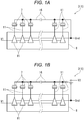
- FIGS. 1A and 1B are diagrams illustrating a schematic configuration of an electric circuit of an inkjet head 3 according to a first embodiment.
- FIG. 1A illustrates an example
- FIG. 1B illustrates a modification example.
- An inkjet printer 1 includes a plurality of inkjet heads 3.
- the inkjet printer 1 includes an ink supplying section that supplies ink toward the inkjet heads 3, a medium conveying section that conveys a recording medium toward the inkjet heads 3, and a printer control section.
- Each of the inkjet heads 3 includes a plurality of actuators 7 and a driving IC 8.
- the driving IC 8 includes a driving circuit including output transistors 8T.
- each actuator 7 is connected to an individual wire 11.
- the other end of each actuator 7 is connected to a common wire 16.
- the individual wires 11 are wires individually connected for each of the actuators 7.
- the individual wires 11 are connected to the driving IC 8.
- the common wire 16 is a shared wire connected to the actuators 7.
- the common wire 16 is grounded. That is, the actuators 7 are connected to a driving circuit of the driving IC 8 via separate individual wires 11 and connected to reference potential GND (0 V) via the common wire 16 shared by actuators 7.
- the driving circuit of the driving IC 8 selectively controls the output transistors 8T to supply a driving potential V1 or a reference potential GND. If the driving circuit of the driving IC 8 controls the output transistors 8T to the driving potential VI, the driving potential V1 is charged in the actuators 7. If the driving circuit of the driving IC 8 controls the output transistors 8T to the reference potential GND, the actuators 7 are discharged to the reference potential GND.
- FIGS. 2A and 2B are diagrams illustrating the inkjet head 3 according to the first embodiment.
- FIG. 2A illustrates the inkjet head 3 before bonding.
- FIG. 2B illustrates the inkjet head 3 after the bonding.
- wires and the like are illustrated as being seen through flexible substrates 20 and a relay substrate 30.
- FIGS. 3A to 3E are diagrams illustrating the inkjet head according to the first embodiment.
- FIG. 3A is a cross-sectional view along A-A in FIG. 2B .
- FIG. 3B is a cross-sectional view along B-B in FIG. 2B .
- FIG. 3C is an enlarged view of a part C in FIG. 2B .
- FIG. 3D is an enlarged view of a part D in FIG. 2B .
- FIG. 3E is an enlarged view of a part E in FIG. 2B .
- FIGS. 3C to 3E for convenience of explanation, only wires are illustrated.
- the inkjet head 3 includes a head substrate 10, flexible substrates 20, and a relay substrate 30.
- the plurality of actuators 7 corresponding to ink chambers, respectively, are disposed on the head substrate 10.
- the flexible substrates 20 and the relay substrate 30 are bonded to the head substrate 10.
- the longitudinal (length) direction of the head substrate 10 is referred to as X direction or left-right direction.
- +X direction is referred to as a right direction and -X direction is referred to as a left direction.
- An end portion (a first end) in -X direction and an end portion (a second end) in +X direction are collectively referred to as both ends.
- the short side (width) direction of the head substrate 10 is referred to as Y direction or up-down direction.
- +Y direction is referred to as an upper direction or an output direction and -Y direction is referred to as a lower direction or an input direction.
- the thickness direction of the head substrate 10 is referred to as Z direction.
- +Z direction is referred to as a front direction and -Z direction is referred to as a rear direction.
- connecting Electrical coupling
- bonding physical coupling
- the head substrate 10, the flexible substrates 20, and the relay substrate 30 are sequentially bonded in Y direction.
- the head substrate 10 is disposed in +Y direction with respect to the flexible substrates 20 and the relay substrate 30 is disposed in -Y direction with respect to the flexible substrates 20.
- Two flexible substrates 20 are disposed in parallel between the head substrate 10 and the relay substrate 30.
- Side edge portions 20a on the output side of the flexible substrates 20 are disposed on a side edge portion 10b on the input side of the head substrate 10.
- Side edge portions 20b on the input side of the flexible substrates 20 are disposed on a side edge portion 30a on the output side of the relay substrate 30.
- FIG. 10 illustrates a perspective view of the inkjet head 3.
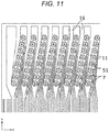
- FIG. 11 illustrates a partially enlarged view of a front surface (nozzle plate) 10s of the head substrate 10.
- the head substrate 10 is a hard single-side substrate made of silicon or glass.
- the plane shape of the head substrate 10 is a rectangle.
- the head substrate 10 includes the plurality of actuators 7.
- the actuators 7 are piezoelectric elements, for example.
- the plurality of actuators 7 are microelectromechanical systems (MEMSs) and disposed on a surface 10s of the head substrate 10.
- the actuator 7, which is a driving source for ejecting ink, is provided for each nozzle 51.
- Each of the actuators 7 is formed in an annular shape, and the actuators 7 are arranged so that the nozzles 51 are located at the center thereof.
- the plurality of actuators 7 are disposed in parallel along the left-right direction.
- the number of the actuators 7 forming one row is, for example, twenty.
- the actuator 7 includes eight actuators 7 arranged in Y axis direction as one set in X axis direction. For example, 150 sets are arranged in X axis direction, and a total of 1200 actuators 7 are arranged.
- a plurality of nozzles 51 for ejecting ink are arranged on a front surface 10s of the head substrate 10.
- the nozzles 51 are two-dimensionally arranged in the column direction (X direction) and the row direction (Y direction). However, the nozzles 51 arranged in the row direction (Y direction) are arranged obliquely so that the nozzles 51 do not overlap on the axis of the Y axis.
- the ink ejected from each nozzle 51 is supplied from the ink supply path 52 communicating with the nozzle 51.
- the head substrate 10 includes the individual wires 11 and the common wire 16. The individual wires 11 and the common wire 16 are connected to the actuators 7.
- the individual wires 11 are a plurality of wires disposed in parallel from the actuators 7 to the side edge portion 10b on the input side on the surface 10s.
- the driving potential V1 or the reference potential GND is supplied to the individual wires 11.
- the number of the individual wires 11 is the same as the number of the actuators 7.
- the number of the individual wires 11 is, for example, 1200.
- Wirings extending from the actuators 7 to the common wire 16 are divided and disposed in parallel to each other from the actuators 7 toward a side edge portion 10a on the output side on the surface 10s. These wirings connected to the actuators 7 are commonly connected to the common wire 16 at the side edge portion 10a, and the common wire 16 is disposed toward left and right both ends along the side edge portion 10a. Further, the common wire 16 is disposed from the left and right both ends of the side edge portion 10a to the side edge portion 10b along side edge portions 10c and 10d on the left and right sides. That is, the common wire 16 is one wire. The common wire 16 is disposed along the side edge portions 10a, 10c, and 10d excluding the side edge portion 10b and further divided from the side edge portion 10a and extending to the actuators 7.
- the reference potential GND is supplied to the common wire 16.
- common wires 16L and 16R are respectively disposed at the left and right both ends.
- the plurality of individual wires 11 are disposed between the common wires 16L and 16R.
- the individual wires 11 are divided into two on the left and right sides of the side edge portion 10b. For example, five hundred individual wires 11 are disposed on the left side and five hundred individual wires are disposed on the right side of the side edge portion 10b.
- the individual wires 11 are divided into two on the left and right sides of the side edge portion 10b, the individual wires 11 are disposed to incline with respect to X direction between the actuators 7 and the side edge portion 10b.
- the individual wires 11 and the common wire 16 are formed of nickel, aluminum, or gold, an alloy of nickel, aluminum, or gold, or the like.
- the film thickness of conductors of the wires is relatively small because the wires are formed by a semiconductor process.
- the individual wires 11 and the common wire 16 have a line thickness of 0.4 ⁇ m (see FIGS. 3A and 3B ).
- the individual wires 11 have a line width of 20 ⁇ m, a wiring interval of 20 ⁇ m, and a disposition interval (pitch) of 40 ⁇ m.
- the common wires 16L and 16R have a line width of 0.8 mm (see FIGS. 3C and 3D ).
- the flexible substrates 20 are single-sided and formed of a synthetic resin film such as polyimide or the like.
- the plane shape of the flexible substrates 20 is rectangular.
- the flexible substrates 20 may be referred to as flexible film circuit boards or flexible printed circuits (FPC) as well.
- a first flexible substrate 20L on the left side and a second flexible substrate 20R on the right side have the same shape and the same configuration.
- Each of the flexible substrates 20 includes one driving IC 8.
- the driving IC 8 is mounted on a rear surface 20t of the flexible substrate 20, which is a surface opposite to a front surface of the flexible substrate 20 depicted in FIG. 2 .
- the driving IC 8 is disposed along the left-right direction in the center of the flexible substrate 20. Terminals of the driving IC 8 are sealed by resin.
- the flexible substrate 20 can be considered a package of the driving IC 8. Therefore, in a sealed state in which the driving IC 8 is mounted on the flexible substrate 20, the flexible substrate 20 may be referred to as a tape carrier package (TCP) or a chip-on-film (COF) package as well.
- TCP tape carrier package
- COF chip-on-film
- Each of the flexible substrates 20 includes output wires 21, input wires 22, a power supply wire 23, a ground wire 24, output monitor wires 25, and common connection wires 26.
- the wires excluding the common connection wires 26 are connected to the driving IC 8. That is, the output wires 21, the input wires 22, the power supply wire 23, the ground wire 24, and the output monitor wires 25 are connected to the driving IC 8.
- the common connection wires 26 are independently provided without being connected to the driving IC 8 and the other wires.
- the output wires 21 are a plurality of wires disposed in parallel from the driving IC 8 to the side edge portion 20a on the output side on the rear surface 20t.
- the output wires 21 are respectively connected to a plurality of output terminals provided on the rear surface of the driving IC 8.
- the driving potential V1 or the reference potential GND is supplied to the output wires 21.
- the number of the output wires 21 is a half of the number of the individual wires 11.
- the number of the output wires 21 is, for example, six hundred.
- the input wires 22 are a plurality of wires disposed in parallel to each other from the driving IC 8 to the side edge portion 20b on the input side on the rear surface 20t.
- the input wires 22 are respectively connected to a plurality of input terminals provided on the rear surface of the driving IC 8.
- a control signal is supplied to the input wires 22.
- the number of the input wires 22 is less than the number of the output wires 21.
- the power supply wire 23 and the ground wire 24 are wires crossing a mounting region of the driving IC 8 in the left-right direction, bent at substantially a right angle on left and right both end sides, and disposed in parallel to each other. That is, the power supply wire 23 and the ground wire 24 are disposed to surround the input wire 22 output side and the left and right both sides.
- the power supply wire 23 is connected to a plurality of power supply terminals provided on the rear surface of the driving IC 8.
- the driving potential V1 is supplied to the power supply wire 23.
- the ground wire 24 is connected to a plurality of ground terminals provided on the rear surface of the driving IC 8.
- the reference potential GND is supplied to the ground wire 24.
- the power supply wire 23 is disposed on the output side and the left-right outer side.
- the ground wire 24 is disposed on the input side and the left-right inner side.
- the output monitor wires 25 are two wires disposed from the driving IC 8 to the side edge portion 20b on the input side. Each of the output monitor wires 25 is connected to one of the plurality of output terminals provided on the rear surface of the driving IC 8. That is, each of the output monitor wires 25 is connected to one of the plurality of output wires 21. A driving waveform that changes between the driving potential V1 and the reference potential GND is supplied to the output monitor wires 25 by the driving IC 8.
- One output monitor 25 is provided on the left side, and one output monitor 25 is provided on the right side.
- the output monitor wires 25 are drawn out from the end portions of the output wires 21, extended from the mounting region of the driving IC 8 to the left and right both ends, and further bent at a right angle and disposed to the side edge portion 20b.
- the output monitor wires 25 are disposed on the output side and the left-right outer side of the power supply wire 23 and disposed in parallel to the power supply wire 23.
- the common connection wires 26 are two wires disposed in the up-down direction along left and right side edge portions 20c and 20d on the rear surface 20t. That is, a common connection wire 26L is disposed at the leftmost edge and a common connection wire 26R is disposed at the rightmost edge.
- the common connection wires 26L and 26R are disposed to directly connect the side edge portion 20b and the side edge portion 20a without being connected to the driving IC 8 and the like.
- the reference potential GND is supplied to the common connection wires 26.
- ground wire 24 and the common connection wires 26 are separated from each other. In other words, the ground wire 24 and the common connection wires 26 are connected to the relay substrate 30 independently from each other and connected to each other on the relay substrate 30.
- the plurality of input wires 22 are disposed side by side at the side edge portion 20b of the flexible substrate 20.
- the ground wire 24 is disposed on the outer side of the plurality of input wires 22.
- the power supply wire 23 is disposed on the outer side of the ground wire 24. Since the flexible substrate 20 is single-sided, the wires on the flexible substrate 20 cannot extend across the other wires.
- the common connection wires 26 and the driving IC 8 are separated on the flexible substrate 20. Therefore, paths of the output monitor wires 25 can be disposed to start from any ones of the output wires 21, pass between the common connection wires 26 and the power supply wire 23, and reach the side edge portion 20b without extending across the other wires.
- the power supply wire 23 is not always disposed on the outer side of the ground wire 24.
- the ground wire 24 may be disposed on the outer side of the power supply wire 23.
- the output wires 21, the input wires 22, the power supply wire 23, the ground wire 24, the output monitor wires 25, and the common connection wires 26 are formed of copper. These wires are formed by laminating the copper on a polyimide film using an adhesive or with electrolytic plating and thereafter patterning the copper. Therefore, these wires have a larger conductor thickness compared with the wires (the individual wires 11 and the common wire 16) on the head substrate 10. These wires have a line thickness of 8 ⁇ m (see FIGS. 3A and 3B ).
- the output wires 21 have a disposition interval (pitch) of 40 ⁇ m, which is the same as the disposition interval of the individual wires 11.
- the output wires 21 have a line width of 18 ⁇ m, which is smaller than the line width of the individual wires 11.
- the output wires 21 have a wiring interval of 22 ⁇ m, which is larger than the wiring interval of the individual wires 11 (see FIG. 3D ).
- the conductors (e.g., wires) on the flexible substrate 20 have thickness approximately twenty times the thickness of the conductors on the head substrate 10. Therefore, the sheet resistance of the conductors on the flexible substrate 20 is substantially lower than the conductors on the head substrate 10. Wiring resistance greatly increases if the line width of the conductors on the head substrate 10, which have high sheet resistance, is reduced. On the other hand, the resistance increase would be relatively small even if the line width of the conductors on the flexible substrate 20, which have a low sheet resistance, is reduced.
- the width of the output wires 21 on the polyimide film is set as narrow as 18 ⁇ m and the wiring interval of the output wires 21 is set as wide as 22 ⁇ m. Consequently, it is possible to prevent an insulation failure even if deviation occurs during connection while reducing the resistance increase.
- the common connection wires 26 have a line width of 0.4 mm, which is a half of the line width of the common wires 16L and 16R (see FIG. 3C ).
- the conductors (e.g., the wires) on the flexible substrate 20 have a thickness approximately twenty times the thickness of the conductors on the head substrate 10. Therefore, the sheet resistance of the conductors on the flexible substrate 20 is lower than the sheet resistance of the conductors on the head substrate 10. Wiring resistance greatly increases if the line width of the conductors on the head substrate 10, which have high sheet resistance, is reduced. On the other hand, a resistance increase would be relatively small if the line width of the conductors on the flexible substrate 20, which have a low sheet resistance, is reduced. It is thus possible to reduce the length in X direction of the polyimide film while limiting a resistance increase by setting the width of the conductors of the common connection wires 26 on the polyimide film side to 0.4 mm. Consequently, it is possible to improve bonding of the flexible substrate 20 and the head substrate 10, reduce manufacturing cost, and reduce cost of the film.
- the common connection wires 26L and 26R are disposed at the left and right both ends.
- the plurality of output wires 21 are disposed in the center of the side edge portion 20a.
- the common connection wire 26L is connected to the common wire 16L and the output wires 21 are respectively connected to the individual wires 11 (connected parts).
- the common connection wire 26R of the flexible substrate 20L may not be connected to any wires of the head substrate 10 and the relay substrate 30, and therefore may be referred to as a dummy wire.
- the common connection wire 26R is connected to the common wire 16R and the output wires 21 are respectively connected to the individual wires 11 (connected parts).
- the flexible substrate 20 and the head substrate 10 are connected via an anisotropic conductive film (ACF).
- ACF anisotropic conductive film
- the ACF is disposed between the side edge portion 20a of the rear surface 20t of the flexible substrate 20 and the side edge portion 10b of the surface 10s of the head substrate 10.
- the flexible substrate 20 and the head substrate 10 can be bonded and the wires can be electrically connected.
- the common wires 16L and 16R and the common connection wires 26L and 26R are electrically connected.
- the common connection wire 26L of the flexible substrate 20L may not be connected to any wires of the head substrate 10 and the relay substrate 30, and therefore may be referred to as a dummy wire.
- the disposition interval (pitch) may be formed narrow than 40 ⁇ m in a state before connection and increased to 40 ⁇ m after the connection.
- the common connection wires 26L and 26R are disposed at the left and right both ends.
- the plurality of input wires 22 are disposed in the center of the side edge portion 20b.
- the output monitor wires 25, the power supply wire 23, and the ground wire 24 are disposed between the common connection wire 26L and the input wires 22.
- the output monitor wires 25, the power supply wire 23, and the ground wire 24 are disposed between the common connection wire 26R and the input wires 22.
- the line width, the wiring interval, and the arrangement interval (pitch) of the input wirings 22 are 0.15 mm, 0.15 mm, and 0.3 mm, respectively (see FIG. 3E ).
- the line width of the output monitor wirings 25 is 100 ⁇ m.
- the line widths of the power source wiring 23, the ground wiring 24, and the common connection wiring 26 are 0.4 mm.
- the relay substrate 30 is a hard substrate obtained by laminating epoxy resin layers with glass fibers and copper wiring layers.
- the relay substrate 30 may be a printed circuit board or the like.
- the relay substrate 30 may be referred to as a "printed board” in some contexts.
- the plane shape of the relay substrate 30 is rectangular.
- the relay substrate 30 includes electronic components and connectors.
- the relay substrate 30 also includes input wires 32, a power supply wire 33, a ground wire 34, and output monitor wires 35.
- the input wires 32, the power supply wire 33, and the ground wire 34 are connected to the connectors.
- the output monitor wires 35 are connected to monitor pins 37 vertically provided on a surface 30s of the relay substrate 30.
- the input wires 32 are disposed in parallel to each other from the side edge portion 30a on the output side toward the connectors.
- the input wires 32 are exposed on the surface 30s at the side edge portion 30a and disposed in an inner layer in portions other than the side edge portion 30a.
- the number of the input wires 32 is the same as the number of the input wires 22.
- a control signal for the driving IC 8 is input (supplied) to the input wires 32 from the printer control section by serial communication. That is, a control signal for controlling the actuators 7 is input (supplied) to the input wires 32 from the printer control section via the connectors and the like.
- the power supply wire 33 and the ground wire 34 are wires disposed in parallel to each other from the side edge portion 30a toward the connectors.
- the power supply wire 33 is exposed on the surface 30s at the side edge portion 30a and disposed in an inner layer in portions other than the side edge portion 30a.
- the ground wire (a reference potential wire) 34 is exposed on the surface 30s at the side edge portion 30a.
- the power supply wire 33 is divided into four at the side edge portion 30a. Two power supply wires 33 are disposed on the left side, and two power supply wires 33 are disposed on the right side of the side edge portion 30a.
- the driving potential V1 for driving the actuators 7 is supplied to the power supply wire 33 from the power supply section (see FIG. 2B ) via the connectors and the like.
- the ground wire 34 is divided into six at the side edge portion 30a. Two ground wires 34 are disposed on the left side and two ground wires 34 are disposed on the right side of the side edge portion 30a. Further, one ground wire 34 is disposed at the left end and one ground wire 34 is disposed at the right end of the side edge portion 30a (ground wires 34L and 34R).
- the two ground wires 34 are disposed in parallel to each other on the inner side of the two power supply wires 33.
- the ground wires 34L and 34R are disposed in parallel to each other on the outer side of the power supply wire 33.
- the reference potential GND for discharging the actuators 7 is supplied to the ground wire 34 from the power supply section via the connectors.
- the output monitor wires 35 are four wires disposed from the side edge portion 30a to four monitor pins 37.
- the four monitor pins 37 may be disposed in any places on the surface 30s of the relay substrate 30.
- the driving waveform can be monitored by connecting a measuring device such as an oscilloscope to the four monitor pins 37.
- the output monitor wires 35 are exposed to the surface 30s at the side edge portion 30a and disposed in an inner layer in portions other than the side edge portion 30a.
- the output monitor wires 35 are disposed on the outer side of the power supply wire 33. In the center of the side edge portion 30a, the two output monitor wires 35 are disposed in parallel to each other. At the left and right both ends of the side edge portion 30a, the output monitor wires 35 are disposed in parallel to each other between the ground wires 34L and 34R and the power supply wire 33.
- the input wires 32, the power supply wire 33, the ground wire 34, and the output monitor wires 35 are formed of copper.
- the input wires 32, the power supply wire 33, the ground wire 34, and the output monitor wires 35 have a line thickness of 35 ⁇ m (see FIGS. 3A and 3B ).
- the conductors (the wires) on the relay substrate 30 have a larger line thickness compared with the conductors on the flexible substrate 20.
- the input wires 32 have a arrangement interval (pitch) of 0.3 mm, which is the same as the arrangement interval of the input wires 22.
- the input wires 32 have a line width of 0.1 mm, which is smaller than the line width of the input wires 22.
- the input wires 32 have a wiring interval of 0.2 mm, which is larger than the wiring interval of the input wires 22 (see FIG. 3E ).
- the conductors (e.g., the wires) on the relay substrate 30 have thickness approximately four times the thickness of the conductors on flexible substrate 20, the sheet resistance of the conductors on the relay substrate 30 is smaller than compared with the wires on the head substrate 10. Therefore, in the relay substrate 30, a resistance increase would be relatively small even if the line width of the conductors is reduced.
- the width of the conductors on the input wires 32 on the relay substrate side, where the influence of the resistance increase would be relatively small even if the width of the conductors is reduced, is set to 0.1 mm to be smaller than the width 0.15 mm of the conductors of the input wires 22. Consequently, it is possible to prevent an insulation failure even if deviation occurs during connection while reducing the resistance increase by setting the wiring interval of the input wires 32 as wide as 0.2 mm.
- the relation between the input wires 32 on the relay substrate 30 and the input wires 22 on the flexible substrate 20 is the same as the relation between the individual wires 11 on the head substrate 10 and the output wires 21 on the flexible substrate 20 explained above.
- a line width and a wiring interval of first wires on the first wiring board having a larger sheet resistance can be set to 1:1. Even if second wires on a second wiring board have a smaller sheet resistance and the same pitch as the pitch of the first wires, a line width of the second wires could be set narrower than a wiring interval of the second wires. Consequently, it is possible to obtain connection that is less likely to cause an insulation failure even if deviation occurs during connection while reducing a resistance increase.
- the power supply wire 33 and the ground wire 34 have a line width of 0.4 mm.
- the output monitor wires 35 have a line width of 100 ⁇ m.
- the ground wire 34L, the output monitor wires 35, the power supply wire 33, the ground wire 34, the plurality of input wires 32, the ground wire 34, the power supply wire 33, and the output monitor wires 35 are disposed in this order from the left side toward the center.
- the ground wire 34R, the output monitor wires 35, the power supply wire 33, the ground wire 34, the plurality of input wires 32, the ground wire 34, the power supply wire 33, and the output monitor wires 35 are disposed in this order from the right side toward the center.
- the wires are connected. That is, the input wires 32 are connected to the input wires 22, the power supply wire 33 is connected to the power supply wire 23, the ground wire 34 is connected to the ground wire 24, the output monitor wires 35 are connected to the output monitor wires 25, and the ground wire 34L is connected the common connection wire 26L on the flexible substrate 20L.
- the wires are connected. That is, the input wires 32 are connected to the input wires 22, the power supply wire 33 is connected to the power supply wire 23, the ground wire 34 is connected to the ground wire 24, the output monitor wires 35 are connected to the output monitor wires 25, and the ground wire 34R is connected to the common connection wire 26R on the flexible substrate 20R.
- the relay substrate 30 and the two flexible substrates 20 are connected via ACFs.
- the ACFs are disposed between the side edge portion 30a of the surface 30s of the relay substrate 30 and the side edge portions 20b of the rear surfaces 20t of the flexible substrates 20.
- the relay substrate 30 and the two flexible substrates 20 are bonded. Further, the wires are electrically connected.
- the common connection wires 26L and 26R and the ground wires 34L and 34R are electrically connected.
- FIG. 4 is a diagram illustrating the flexible substrates 20 formed in a sprocket film F.
- the flexible substrates 20 are illustrated as being seen through a synthetic resin film.
- a plurality of flexible substrates 20 are formed to be continuous on the sprocket film F made of synthetic resin such as polyimide.
- the plurality of flexible substrates 20 are supplied to an assembly factory or the like for the inkjet heads 3 while still in the sprocket film F state.
- the outer peripheries (depicted as broken lines in FIG. 4 ) are cut.
- the flexible substrates 20 can be bonded to the head substrate 10 and the like as the flexible substrates 20 (20L and 20R).
- the inkjet head 3 it is possible to avoid complicated and thin common wires (e.g., the ground wire 24 and the common connection wires 26) on the flexible substrate 20 on which the driving IC 8 that drives the actuators 7 is mounted. Therefore, the inkjet head 3 is less likely to be affected by noise. It is possible to provide the inkjet printer 1 that can prevent deterioration in a discharge characteristic.
- the common wire 16 formed in the head substrate 10 of the inkjet head 3 has the line thickness (the conductor thickness) of 0.4 ⁇ m and is extremely thin. Unlike the individual wires 11, a large electric current flows to the common wire 16 because driving currents of all the actuators 7 gather in the common wire 16. Therefore, the common wire 16 needs to have a line width (a conductor width) eighty times the line width of the individual wires 11. Accordingly, the two common wires 16 having a line width of 0.8 mm are disposed at the side edge portion 10b.
- the common connection wires 26 formed on the flexible substrates 20 have the line thickness of 8 ⁇ m and have thickness twenty times the thickness of the common wire 16. Therefore, even if the line width of the common connection wires 26 is a half (0.4 mm) of the line width (0.8 mm) of the common wire 16, the common connection wires 26 have low electric resistance because a conductor cross-sectional area is large. If positional deviation in the left-right direction occurs in the bonding of the head substrate 10 and the flexible substrates 20, it is likely that parts of the common wire 16 and the common connection wires 26 are connected and electric resistance of the connected parts increases.
- the common connection wires 26 having the small line width are superimposed on and connected to the common wire 16 having the large line width. Therefore, the common connection wires 26 can be surely disposed within a range of the line width of the common wire 16.
- the common wire 16 having a small conductor cross-sectional area and high electric resistance is completely connected to the common connection wires 26 having a large conductor cross-sectional area and low electric resistance. Therefore, an increase in the electric resistance of the connected parts can be avoided.
- the bonding can be performed with a more tolerant positioning margin.
- the ground wires 34L and 34R that supply the reference potential GND to only the actuators 7 are disposed on the relay substrate 30. Therefore, it is possible to optionally control a reference voltage supplied to the actuators 7 by providing switches or the like in the ground wires 34L and 34R.
- negative potential V2 can be supplied to the actuators 7 by switching the switches. Consequently, polarization processing of the actuators 7 can be performed.
- a bias voltage applied to the actuators 7 can be adjusted by varying the potential V2.
- the common connection wires 26 that supply the reference potential to the actuators 7 and the ground wire 24 that supplies the reference potential to the driving IC 8 are separately and independently provided on the flexible substrate 20.
- the output monitor wires 25 can be disposed between the output wires 21 of the driving IC 8 and the common connection wires 26.
- the output monitor wires 25 are connected to any ones of the plurality of output terminals of the driving IC 8 and connected to the output monitor wires 35 of the relay substrate 30
- an output waveform of the driving IC 8 can be monitored on the relay substrate 30. In other words, unlike the past, it is unnecessary to monitor the output waveform of the driving IC 8 on the flexible substrate 20.
- FIGS. 5A and 5B are diagrams illustrating an inkjet head 4 according to a second embodiment.
- FIG. 5A illustrates the inkjet head 4 before bonding.
- FIG. 5B illustrates the inkjet head 4 after the bonding.
- wires and the like are illustrated as being seen through flexible substrates 40 and the relay substrate 30.
- the inkjet head 4 includes the head substrate 10, the flexible substrates 40, and the relay substrate 30. Two flexible substrates 40 are disposed in parallel between the head substrate 10 and the relay substrate 30.
- the flexible substrates 40 have substantially the same configuration as the flexible substrates 20.
- a flexible substrate 40L on the left side does not include the common connection wire 26R.
- a flexible substrate 40R on the right side does not include the common connection wire 26L. That is, the flexible substrate 40L is obtained by removing the common connection wire 26R from the flexible substrate 20. The flexible substrate 40R is obtained by removing the common connection wire 26L from the flexible substrate 20.
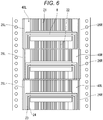
- FIG. 6 is a diagram illustrating the flexible substrates 40 formed in the sprocket film F.
- the flexible substrates 40 are illustrated as being seen through a synthetic resin film.
- a plurality of flexible substrates 40 are formed to be continuous on the sprocket film F.
- the plurality of flexible substrates 40 are supplied to an assembly factory or the like of the inkjet heads 4 while still in the sprocket film F state.
- the flexible substrate 40 formed in the sprocket film F has the same configuration as the configuration of the flexible substrate 20 according to the first embodiment. That is, the flexible substrate 40 formed in the sprocket film F includes two common connection wires 26.
- the common connection wire 26L is left on the sprocket film F (depicted as a broken line in FIG. 6 ). That is, the common connection wire 26L is removed from the flexible substrate 40.
- the flexible substrate 40 can be bonded to the head substrate 10 or the like as the flexible substrate 40R.
- the common connection wire 26R is left on the sprocket film F (depicted as a broken line in FIG. 6 ). That is, the common connection wire 26R is removed from the flexible substrate 40.
- the flexible substrate 40 can be bonded to the head substrate 10 or the like as the flexible substrate 40L.
- the inkjet head 4 achieves the same operational effect as the operational effect of the inkjet head 3. That is, it is possible to avoid complication and thinning of the common wires (e.g., the ground wire 24 and the common connection wires 26) on the flexible substrate 40 on which the driving IC 8 that drives the actuators 7 is mounted. Therefore, it is possible to provide the inkjet printer 1 that can prevent deterioration in a discharge characteristic.
- the common wires e.g., the ground wire 24 and the common connection wires 26
- the inkjet head 4 can improve manufacturing efficiency. That is, if the respective flexible substrates 40 are cut off from the sprocket film F, cut lines are varied. Consequently, it is possible to cut out the flexible substrates 40L and 40R from the sprocket film F on which the plurality of flexible substrates 40 all have the same initial configuration.
- the flexible substrate 40L on the left side does not include the common connection wire 26R and the flexible substrate 40R on the right side does not include the common connection wire 26L. Therefore, the width of the two flexible substrates 40 is smaller compared with the first embodiment. Consequently, in the head substrate 10, the plurality of individual wires 11 divided into two to the left and the right can be disposed close to the center. That is, an arranging direction of the individual wires 11 can be aligned with the up-down direction.
- FIGS. 12A and 12B are diagrams illustrating enlarged views of ink jet heads, where FIG. 12A illustrates two flexible substrates separated from each other, and FIG. 12B illustrates two flexible substrates arranged in the vicinity of each other.
- an inclination of the discrete wirings 11 at a center region corresponding to a space between the two flexible substrate 40 can be decreased by disposing the two flexible substrates 40 close to each other in the left-right direction as in FIG. 12B as opposed to that shown in FIG. 12A .
- the individual wires 11 can be formed to extend along X direction. Consequently, the electric resistances of the individual wires 11 can become more uniform. The insulation reliability is improved.
- the yield of the head substrate 10 can be increased.
- FIG. 7 is a diagram illustrating an inkjet head 5 according to a third embodiment. For convenience of explanation, wires and the like are illustrated as being seen through flexible substrates 40 and the relay substrate 30.
- the inkjet head 5 includes the head substrate 10, the flexible substrates 40, and the relay substrate 30.
- Three flexible substrates 40L, 40C, and 40R are disposed in parallel to each other between the head substrate 10 and the relay substrate 30.
- the flexible substrate 40L on the left side does not include the common connection wire 26R.
- the flexible substrate 40R on the right side does not include the common connection wire 26L.
- the flexible substrate 40C in the center does not include the common connection wires 26. That is, the flexible substrate 40C is obtained by removing the two common connection wires 26 from the flexible substrate 20.
- FIG. 8 is a diagram illustrating the flexible substrates 40 formed in the sprocket film F.
- the flexible substrates 40 are illustrated as being seen through a synthetic resin film.
- the flexible substrates 40 are formed continuously along length of the sprocket film F.
- the flexible substrates 40 formed in the sprocket film F each include the two common connection wires 26.
- the common connection wire 26L is left on the sprocket film F (depicted as a broken line in FIG. 8 ).
- the common connection wire 26L is removed from the flexible substrate 40.
- the flexible substrate 40 can be bonded to the head substrate 10 or the like as the flexible substrate 40R.
- the common connection wires 26L and 26R are left on the sprocket film F (a broken line in FIG. 8 ).
- the common connection wire 26R is removed from the flexible substrate 40.
- the flexible substrate 40 can be bonded to the head substrate 10 or the like as the flexible substrate 40C.
- the common connection wire 26R is left on the sprocket film F (depicted as a broken line in FIG. 8 ).
- the common connection wire 26R is removed from the flexible substrate 40.
- the flexible substrate 40 can be bonded to the head substrate 10 or the like as the flexible substrate 40L.
- the inkjet head 5 achieves the same operational effect as the operational effect of the inkjet heads 3 and 4. That is, it is possible to avoid complicated and thin common wires (e.g., the ground wire 24 and the common connection wires 26) on the flexible substrate 40 on which the driving IC 8 that drives the actuators 7 is mounted. Therefore, the inkjet head 5 is less likely to be affected by noise. It is possible to provide the inkjet printer 1 that can prevent deterioration in a discharge characteristic. Further, like the inkjet head 4, the inkjet head 5 can improve manufacturing efficiency. That is, when the respective flexible substrates 40 are cut from the sprocket film F, cut lines can be varied. Consequently, it is possible to cut out the flexible substrates 40L, 40C, and 40R from a sprocket film F on which a plurality of flexible substrates 40 having the same configuration have been formed.
- the inkjet head 5 can improve manufacturing efficiency. That is, when the respective flexible substrates 40 are cut from the sprocket film F, cut
- the flexible substrate 40L on the left side does not include the common connection wire 26R
- the flexible substrate 40R on the right side does not include the common connection wire 26L
- the flexible substrate 40C does not include the common connection wires 26.
- FIG. 9 is a diagram illustrating an inkjet head 6 according to a fourth embodiment.
- wires and the like are illustrated as being seen through the flexible substrate 20 and the relay substrate 30.
- the inkjet head 6 includes the head substrate 10, the flexible substrate 20, and the relay substrate 30.
- One flexible substrate 20 is disposed between the head substrate 10 and the relay substrate 30.
- the inkjet head 6 achieves the same operational effect as the operational effect of the inkjet heads 3 to 5. That is, it is possible to avoid complication and thinning of the common wires (e.g., the ground wire 24 and the common connection wires 26) on the flexible substrate 20 on which the driving IC 8 that drives the actuator 7 is mounted. Therefore, the inkjet head 6 is less likely to be affected by noise. It is possible to provide the inkjet printer 1 that can prevent deterioration in a discharge characteristic. In the embodiments explained above, only one driving IC 8 may not necessarily be mounted on one flexible board. Two or more driving ICs 8 may be mounted on one flexible substrate. In this case, the two or more driving ICs 8 are disposed in series along the left-right direction.
- Elements that cause the nozzles to discharge the ink are not limited to the actuators 7 formed by the piezoelectric elements.
- the elements may be heaters or solenoid valves, for example.
- the substrate shapes are not limited to rectangular and may be a parallelogram, a trapezoid, or the like.
- the wires are not always linearly disposed or disposed in parallel. Various changes can be performed according to necessity.
Landscapes
- Engineering & Computer Science (AREA)
- Manufacturing & Machinery (AREA)
- Particle Formation And Scattering Control In Inkjet Printers (AREA)
- Structure Of Printed Boards (AREA)
Abstract
Description
- The present invention relates to the field of an electric circuit in general, and embodiments described herein relate in particular to an inkjet head, an inkjet printer, and a manufacturing method for the inkjet head.
- An inkjet head includes a channel forming member in which a plurality of ink chambers are formed, a nozzle plate on which a plurality of nozzles that communicate with the ink chambers are formed, and a head substrate on which a plurality of elements, such as actuators, corresponding to the ink chambers are disposed.
- The head substrate may be connected to a printer control section via a flexible substrate, a relay substrate, a cable, or the like. A driving integrated circuit (IC) chip that drives the plurality of elements may be mounted on the flexible substrate.
- Driving power is output from the driving IC chip in accordance with a command from the printer control section and supplied to the elements. Consequently, deformation, heat generation, or the like of the elements occurs, an ink pressure in pressure chambers increases, and ink is thus ejected from the nozzles. Individual wires for supplying a driving signal and a common wire for supplying reference potential (ground potential) are connected to the elements.
- The common wire may be disposed in a separate path not on the flexible substrate or disposed through the driving IC chip on the flexible substrate.
- If the common wire is disposed in a path separate from the flexible substrate, wiring may become long and complicated. Therefore, the common wire is more likely to be affected by noise or deterioration in a discharge characteristic due to a voltage drop is caused. Wire connecting work may be also complicated.
- If the common wire is disposed through the driving IC chip on the flexible substrate, malfunction of the driving IC may occur because of noise propagating in the common wire. The common wire may need to be formed with a thin width, which may cause deterioration in discharge characteristics due to a voltage drop. If the common wire is widened, a mounting area of the driving IC chip may increase and a reduction in the size of an apparatus may be hindered.
- To solve such problem, there is provided an ink jet head, comprising: a head substrate including thereon: a plurality of ink jet elements configured to cause ink to be ejected from a plurality of nozzles; and a common wire extending from an edge of the head substrate and electrically connected to the ink jet elements in common; a printed board with a reference potential wire through which a reference potential is provided to the ink jet head; and a plurality of flexible substrates connected in parallel to each other between the head substrate and the printed board, wherein a first one of the flexible substrates at a first end of an arrangement of the plurality of flexible substrates and a second one of the flexible substrates at a second end of the arrangement of the plurality of flexible substrates each has a common connection wire electrically connected between the common wire and the reference potential wire.
- Preferably, the common connection wire of the first one of the flexible substrates is disposed along an outside edge thereof, and the common connection wire of the second one of the flexible substrates is disposed along an outside edge thereof.
- Preferably still, the plurality of flexible substrates includes at least three flexible substrates in total.
- Preferably yet, a third one of the flexible substrates is between the first one of the flexible substrates and the second one of the flexible substrates in the arrangement of the plurality of flexible substrate.
- Suitably, the third one of the flexible substrates has no common connection wire electrically connected between the common wire and the reference potential wire.
- Suitably still, the third one of the flexible substrates has a dummy wire at a position of the third one of the flexible substrates corresponding to a position of the common connection wire on the first one of the flexible substrates.
- Suitably yet, the dummy wire is electrically isolated from any wire on the head substrate and any wire on the printed board.
- Typically, a wire arrangement of the third one of the flexible substrates is the same as a wire arrangement of the first one of the flexible substrates except for the common connection wire thereof.
- Typically still, a wire arrangement of the third one of the flexible substrates is the same as a wire arrangement of the first one of the flexible substrates except for the common connection wire thereof.
- Typically yet, the first one of the flexible substrates further includes a dummy wire extending between first and second edges thereof along an inside edge opposite to the outside edge.
- Preferably, the dummy wire is electrically isolated from any wire on the head substrate and any wire on the printed board.
- Preferably still, the common connection wire and the dummy wire are disposed symmetrically with respect to a center line of the first one of the flexible substrates extending between the first and second edges.
- Preferably yet, a wire arrangement of the first one of the flexible substrates except for the common connection wire thereof is the same as a wire arrangement of the second one of the flexible substrates except for the common connection wire thereof.
- Suitably, the first one of the flexible substrates includes no wire extending between first and second edges thereof at a position along an inside edge opposite to the outside edge, and the second one of the flexible substrates includes no wire extending between first and second edges thereof at a position along an inside edge opposite to the outside edge.
- Suitably still, a wire arrangement of the first one of the flexible substrates except for the common connection wire thereof is the same as a wire arrangement of the second one of the flexible substrates except for the common connection wire thereof.
- Suitably yet, a wire arrangement of the first one of the flexible substrates and a wire arrangement of the second one of the flexible substrates are symmetrical with respect to a center of the head substrate.
- The invention also relates to a method for manufacturing an ink jet head, comprising: forming a sprocket film including a plurality of flexible substrate regions, each flexible substrate region including: a first wire extending between a first end of the flexible substrate region and a second end of the substrate region opposite the first end along a third end of the flexible substrate region, a second wire extending between the first and second ends of the flexible substrate region along a fourth end of the flexible substrate region opposite to the third end, and a plurality of drive wires to be connected to a drive circuit configured to drive ink jet elements of an ink jet head; cutting a first region from the sprocket film, the cut first region corresponding to a flexible substrate region with an end portion corresponding to the second wire being excluded; and using the cut first region as a first flexible substrate having a drive circuit mounted thereon.
- Preferably, the method further comprises: cutting a second region from the sprocket film, the cut second region corresponding to a flexible substrate region with an end portion corresponding to the first wire being excluded; and using the cut second region as a second flexible substrate having a second drive circuit mounted thereon, the second flexible substrate being connected to a head substrate including ink jet elements in parallel with the first flexible substrate.
- Preferably still, the method further comprises: cutting a third region from the sprocket film, the cut third region corresponding to a flexible substrate region with an end portion corresponding to the first wire and an end portion corresponding to the second wire being excluded; and using the cut third region as a third flexible substrate having a third drive circuit mounted thereon, the third flexible substrate being between the first flexible substrate and the second flexible substrate and connected in parallel with the first flexible substrate and the second flexible substrate.
- Preferably yet, the method further comprises: connecting the first wire of the first flexible substrate to a common wire of a head substrate that is electrically connected to common terminals of ink jet elements.
- The above and other objects, features and advantages of the present invention will be made apparent from the following description of the preferred embodiments, given as non-limiting examples, with reference to the accompanying drawings, in which:
-
FIGS. 1A and 1B are diagrams illustrating a schematic configuration of an electric circuit of an inkjet head according to a first embodiment,FIG. 1A illustrating a general example andFIG. 1B illustrating a modification. -
FIGS. 2A and 2B are diagrams illustrating the inkjet head,FIG. 2A illustrating the inkjet head before bonding andFIG. 2B illustrating the inkjet head after the bonding. -
FIGS. 3A and 3E are diagrams illustrating the inkjet head,FIG. 3A being a cross-sectional view along A-A inFIG. 2B ,FIG. 3B being a cross-sectional view along B-B inFIG. 2B ,FIG. 3C being an enlarged view of a part C inFIG. 2B ,FIG. 3D being an enlarged view of a part D inFIG. 2B , andFIG. 3E being an enlarged view of a part E inFIG. 2B . -
FIG. 4 is a diagram illustrating flexible substrates formed in a sprocket film.FIGS. 5A and 5B are diagrams illustrating an inkjet head according to a second embodiment,FIG. 5A illustrating the inkjet head before bonding andFIG. 5B illustrating the inkjet head after the bonding. -
FIG. 6 is a diagram illustrating flexible substrates formed in a sprocket film.FIG. 7 is a diagram illustrating an inkjet head according to a third embodiment. -
FIG. 8 is a diagram illustrating flexible substrates formed in a sprocket film.FIG. 9 is a diagram illustrating an inkjet head according to a fourth embodiment. -
FIG. 10 illustrates a perspective view of the inkjet head. -
FIG. 11 illustrates a partially enlarged view of a front surface of the head substrate. -
FIGS. 12A and 12B are diagrams illustrating enlarged views of ink jet heads, whereFIG. 12A illustrates two flexible substrates separated from each other, andFIG. 12B illustrates two flexible substrates arranged in the vicinity of each other. - An embodiment is directed to providing an inkjet head, an inkjet printer, a manufacturing method for the inkjet head that can avoid complication and thinning of a common wire on a flexible substrate on which a driving IC that drives a plurality of elements is mounted and prevent deterioration in discharge characteristics.
- An ink jet head includes a head substrate, a printed board, and a plurality of flexible substrates connected in parallel to each other between the head substrate and the printed board. The head substrate includes thereon a plurality of ink jet elements configured to cause ink to be ejected from a plurality of nozzles, and a common wire extending from an edge of the head substrate and electrically connected to the ink jet elements in common. The printed board includes, thereon, a reference potential wire through which a reference potential is set to the ink jet head. A first one of the flexible substrates at a first end of an arrangement of the flexible substrates and a second one of the flexible substrates at a second end of the arrangement of the flexible substrates opposite to the first end each has a common connection wire electrically connected between the common wire and the reference potential wire.
- Inkjet heads and inkjet printers according to example embodiments are explained below with reference to the drawings. In the figures, the same components are denoted by the same reference numerals and signs.
-
FIGS. 1A and 1B are diagrams illustrating a schematic configuration of an electric circuit of aninkjet head 3 according to a first embodiment.FIG. 1A illustrates an example, andFIG. 1B illustrates a modification example. - An
inkjet printer 1 includes a plurality of inkjet heads 3. Theinkjet printer 1 includes an ink supplying section that supplies ink toward the inkjet heads 3, a medium conveying section that conveys a recording medium toward the inkjet heads 3, and a printer control section. - Each of the inkjet heads 3 includes a plurality of
actuators 7 and a drivingIC 8. The drivingIC 8 includes a driving circuit includingoutput transistors 8T. - One end of each
actuator 7 is connected to anindividual wire 11. The other end of eachactuator 7 is connected to acommon wire 16. - The
individual wires 11 are wires individually connected for each of theactuators 7. Theindividual wires 11 are connected to the drivingIC 8. Thecommon wire 16 is a shared wire connected to theactuators 7. Thecommon wire 16 is grounded. That is, theactuators 7 are connected to a driving circuit of the drivingIC 8 via separateindividual wires 11 and connected to reference potential GND (0 V) via thecommon wire 16 shared byactuators 7. - The driving circuit of the driving
IC 8 selectively controls theoutput transistors 8T to supply a driving potential V1 or a reference potential GND. If the driving circuit of the drivingIC 8 controls theoutput transistors 8T to the driving potential VI, the driving potential V1 is charged in theactuators 7. If the driving circuit of the drivingIC 8 controls theoutput transistors 8T to the reference potential GND, theactuators 7 are discharged to the reference potential GND. -
FIGS. 2A and 2B are diagrams illustrating theinkjet head 3 according to the first embodiment.FIG. 2A illustrates theinkjet head 3 before bonding.FIG. 2B illustrates theinkjet head 3 after the bonding. For convenience of explanation, wires and the like are illustrated as being seen throughflexible substrates 20 and arelay substrate 30. -
FIGS. 3A to 3E are diagrams illustrating the inkjet head according to the first embodiment.FIG. 3A is a cross-sectional view along A-A inFIG. 2B .FIG. 3B is a cross-sectional view along B-B inFIG. 2B .FIG. 3C is an enlarged view of a part C inFIG. 2B .FIG. 3D is an enlarged view of a part D inFIG. 2B .FIG. 3E is an enlarged view of a part E inFIG. 2B . InFIGS. 3C to 3E , for convenience of explanation, only wires are illustrated. - The
inkjet head 3 includes ahead substrate 10,flexible substrates 20, and arelay substrate 30. - On the
head substrate 10, the plurality ofactuators 7 corresponding to ink chambers, respectively, are disposed. Theflexible substrates 20 and therelay substrate 30 are bonded to thehead substrate 10. - In the following explanation, the longitudinal (length) direction of the
head substrate 10 is referred to as X direction or left-right direction. +X direction is referred to as a right direction and -X direction is referred to as a left direction. An end portion (a first end) in -X direction and an end portion (a second end) in +X direction are collectively referred to as both ends. - The short side (width) direction of the
head substrate 10 is referred to as Y direction or up-down direction. +Y direction is referred to as an upper direction or an output direction and -Y direction is referred to as a lower direction or an input direction. - The thickness direction of the
head substrate 10 is referred to as Z direction. +Z direction is referred to as a front direction and -Z direction is referred to as a rear direction. - Electrical coupling is referred to as "connecting" and physical coupling is referred to as "bonding."
- The
head substrate 10, theflexible substrates 20, and therelay substrate 30 are sequentially bonded in Y direction. Thehead substrate 10 is disposed in +Y direction with respect to theflexible substrates 20 and therelay substrate 30 is disposed in -Y direction with respect to theflexible substrates 20. Twoflexible substrates 20 are disposed in parallel between thehead substrate 10 and therelay substrate 30. -
Side edge portions 20a on the output side of theflexible substrates 20 are disposed on aside edge portion 10b on the input side of thehead substrate 10.Side edge portions 20b on the input side of theflexible substrates 20 are disposed on aside edge portion 30a on the output side of therelay substrate 30. -
FIG. 10 illustrates a perspective view of theinkjet head 3.FIG. 11 illustrates a partially enlarged view of a front surface (nozzle plate) 10s of thehead substrate 10. Thehead substrate 10 is a hard single-side substrate made of silicon or glass. The plane shape of thehead substrate 10 is a rectangle. Thehead substrate 10 includes the plurality ofactuators 7. Theactuators 7 are piezoelectric elements, for example. The plurality ofactuators 7 are microelectromechanical systems (MEMSs) and disposed on asurface 10s of thehead substrate 10. Theactuator 7, which is a driving source for ejecting ink, is provided for eachnozzle 51. Each of theactuators 7 is formed in an annular shape, and theactuators 7 are arranged so that thenozzles 51 are located at the center thereof. - The plurality of
actuators 7 are disposed in parallel along the left-right direction. The number of theactuators 7 forming one row is, for example, twenty. In one implementation, theactuator 7 includes eightactuators 7 arranged in Y axis direction as one set in X axis direction. For example, 150 sets are arranged in X axis direction, and a total of 1200actuators 7 are arranged. - A plurality of
nozzles 51 for ejecting ink are arranged on afront surface 10s of thehead substrate 10. Thenozzles 51 are two-dimensionally arranged in the column direction (X direction) and the row direction (Y direction). However, thenozzles 51 arranged in the row direction (Y direction) are arranged obliquely so that thenozzles 51 do not overlap on the axis of the Y axis. The ink ejected from eachnozzle 51 is supplied from the ink supply path 52 communicating with thenozzle 51. Thehead substrate 10 includes theindividual wires 11 and thecommon wire 16. Theindividual wires 11 and thecommon wire 16 are connected to theactuators 7. - The
individual wires 11 are a plurality of wires disposed in parallel from theactuators 7 to theside edge portion 10b on the input side on thesurface 10s. The driving potential V1 or the reference potential GND is supplied to theindividual wires 11. - The number of the
individual wires 11 is the same as the number of theactuators 7. The number of theindividual wires 11 is, for example, 1200. - Wirings extending from the
actuators 7 to thecommon wire 16 are divided and disposed in parallel to each other from theactuators 7 toward aside edge portion 10a on the output side on thesurface 10s. These wirings connected to theactuators 7 are commonly connected to thecommon wire 16 at theside edge portion 10a, and thecommon wire 16 is disposed toward left and right both ends along theside edge portion 10a. Further, thecommon wire 16 is disposed from the left and right both ends of theside edge portion 10a to theside edge portion 10b alongside edge portions common wire 16 is one wire. Thecommon wire 16 is disposed along theside edge portions side edge portion 10b and further divided from theside edge portion 10a and extending to theactuators 7. - The reference potential GND is supplied to the
common wire 16. - At the
side edge portion 10b of thehead substrate 10,common wires individual wires 11 are disposed between thecommon wires individual wires 11 are divided into two on the left and right sides of theside edge portion 10b. For example, five hundredindividual wires 11 are disposed on the left side and five hundred individual wires are disposed on the right side of theside edge portion 10b. - Since the
individual wires 11 are divided into two on the left and right sides of theside edge portion 10b, theindividual wires 11 are disposed to incline with respect to X direction between theactuators 7 and theside edge portion 10b. - The
individual wires 11 and thecommon wire 16 are formed of nickel, aluminum, or gold, an alloy of nickel, aluminum, or gold, or the like. The film thickness of conductors of the wires is relatively small because the wires are formed by a semiconductor process. Specifically, theindividual wires 11 and thecommon wire 16 have a line thickness of 0.4 µm (seeFIGS. 3A and 3B ). - At the
side edge portion 10b, theindividual wires 11 have a line width of 20 µm, a wiring interval of 20 µm, and a disposition interval (pitch) of 40 µm. Thecommon wires FIGS. 3C and 3D ). - The
flexible substrates 20 are single-sided and formed of a synthetic resin film such as polyimide or the like. The plane shape of theflexible substrates 20 is rectangular. Theflexible substrates 20 may be referred to as flexible film circuit boards or flexible printed circuits (FPC) as well. A firstflexible substrate 20L on the left side and a secondflexible substrate 20R on the right side have the same shape and the same configuration. - Each of the
flexible substrates 20 includes one drivingIC 8. The drivingIC 8 is mounted on arear surface 20t of theflexible substrate 20, which is a surface opposite to a front surface of theflexible substrate 20 depicted inFIG. 2 . The drivingIC 8 is disposed along the left-right direction in the center of theflexible substrate 20. Terminals of the drivingIC 8 are sealed by resin. - The
flexible substrate 20 can be considered a package of the drivingIC 8. Therefore, in a sealed state in which the drivingIC 8 is mounted on theflexible substrate 20, theflexible substrate 20 may be referred to as a tape carrier package (TCP) or a chip-on-film (COF) package as well. - Each of the
flexible substrates 20 includesoutput wires 21,input wires 22, apower supply wire 23, aground wire 24,output monitor wires 25, and common connection wires 26. - The wires excluding the common connection wires 26 are connected to the driving
IC 8. That is, theoutput wires 21, theinput wires 22, thepower supply wire 23, theground wire 24, and theoutput monitor wires 25 are connected to the drivingIC 8. - On the other hand, the common connection wires 26 are independently provided without being connected to the driving
IC 8 and the other wires. - The
output wires 21 are a plurality of wires disposed in parallel from the drivingIC 8 to theside edge portion 20a on the output side on therear surface 20t. Theoutput wires 21 are respectively connected to a plurality of output terminals provided on the rear surface of the drivingIC 8. The driving potential V1 or the reference potential GND is supplied to theoutput wires 21. - The number of the
output wires 21 is a half of the number of theindividual wires 11. The number of theoutput wires 21 is, for example, six hundred. - The
input wires 22 are a plurality of wires disposed in parallel to each other from the drivingIC 8 to theside edge portion 20b on the input side on therear surface 20t. Theinput wires 22 are respectively connected to a plurality of input terminals provided on the rear surface of the drivingIC 8. A control signal is supplied to theinput wires 22. - The number of the
input wires 22 is less than the number of theoutput wires 21. - The
power supply wire 23 and theground wire 24 are wires crossing a mounting region of the drivingIC 8 in the left-right direction, bent at substantially a right angle on left and right both end sides, and disposed in parallel to each other. That is, thepower supply wire 23 and theground wire 24 are disposed to surround theinput wire 22 output side and the left and right both sides. - The
power supply wire 23 is connected to a plurality of power supply terminals provided on the rear surface of the drivingIC 8. The driving potential V1 is supplied to thepower supply wire 23. - The
ground wire 24 is connected to a plurality of ground terminals provided on the rear surface of the drivingIC 8. The reference potential GND is supplied to theground wire 24. - One
power supply wire 23 and oneground wire 24 are provided. Thepower supply wire 23 is disposed on the output side and the left-right outer side. Theground wire 24 is disposed on the input side and the left-right inner side. - The
output monitor wires 25 are two wires disposed from the drivingIC 8 to theside edge portion 20b on the input side. Each of theoutput monitor wires 25 is connected to one of the plurality of output terminals provided on the rear surface of the drivingIC 8. That is, each of theoutput monitor wires 25 is connected to one of the plurality ofoutput wires 21. A driving waveform that changes between the driving potential V1 and the reference potential GND is supplied to theoutput monitor wires 25 by the drivingIC 8. - One output monitor 25 is provided on the left side, and one
output monitor 25 is provided on the right side. Theoutput monitor wires 25 are drawn out from the end portions of theoutput wires 21, extended from the mounting region of the drivingIC 8 to the left and right both ends, and further bent at a right angle and disposed to theside edge portion 20b. Theoutput monitor wires 25 are disposed on the output side and the left-right outer side of thepower supply wire 23 and disposed in parallel to thepower supply wire 23. - The common connection wires 26 are two wires disposed in the up-down direction along left and right
side edge portions rear surface 20t. That is, acommon connection wire 26L is disposed at the leftmost edge and acommon connection wire 26R is disposed at the rightmost edge. Thecommon connection wires side edge portion 20b and theside edge portion 20a without being connected to the drivingIC 8 and the like. The reference potential GND is supplied to the common connection wires 26. - The
ground wire 24 and the common connection wires 26 are separated from each other. In other words, theground wire 24 and the common connection wires 26 are connected to therelay substrate 30 independently from each other and connected to each other on therelay substrate 30. - The plurality of
input wires 22 are disposed side by side at theside edge portion 20b of theflexible substrate 20. Theground wire 24 is disposed on the outer side of the plurality ofinput wires 22. Thepower supply wire 23 is disposed on the outer side of theground wire 24. Since theflexible substrate 20 is single-sided, the wires on theflexible substrate 20 cannot extend across the other wires. - However, the common connection wires 26 and the driving
IC 8 are separated on theflexible substrate 20. Therefore, paths of theoutput monitor wires 25 can be disposed to start from any ones of theoutput wires 21, pass between the common connection wires 26 and thepower supply wire 23, and reach theside edge portion 20b without extending across the other wires. - The
power supply wire 23 is not always disposed on the outer side of theground wire 24. Theground wire 24 may be disposed on the outer side of thepower supply wire 23. - The
output wires 21, theinput wires 22, thepower supply wire 23, theground wire 24, theoutput monitor wires 25, and the common connection wires 26 are formed of copper. These wires are formed by laminating the copper on a polyimide film using an adhesive or with electrolytic plating and thereafter patterning the copper. Therefore, these wires have a larger conductor thickness compared with the wires (theindividual wires 11 and the common wire 16) on thehead substrate 10. These wires have a line thickness of 8 µm (seeFIGS. 3A and 3B ). - At the
side edge portion 20a, theoutput wires 21 have a disposition interval (pitch) of 40 µm, which is the same as the disposition interval of theindividual wires 11. Theoutput wires 21 have a line width of 18 µm, which is smaller than the line width of theindividual wires 11. Theoutput wires 21 have a wiring interval of 22 µm, which is larger than the wiring interval of the individual wires 11 (seeFIG. 3D ). - The conductors (e.g., wires) on the
flexible substrate 20 have thickness approximately twenty times the thickness of the conductors on thehead substrate 10. Therefore, the sheet resistance of the conductors on theflexible substrate 20 is substantially lower than the conductors on thehead substrate 10. Wiring resistance greatly increases if the line width of the conductors on thehead substrate 10, which have high sheet resistance, is reduced. On the other hand, the resistance increase would be relatively small even if the line width of the conductors on theflexible substrate 20, which have a low sheet resistance, is reduced. The width of theoutput wires 21 on the polyimide film, is set as narrow as 18 µm and the wiring interval of theoutput wires 21 is set as wide as 22 µm. Consequently, it is possible to prevent an insulation failure even if deviation occurs during connection while reducing the resistance increase. - The common connection wires 26 have a line width of 0.4 mm, which is a half of the line width of the
common wires FIG. 3C ). - The conductors (e.g., the wires) on the
flexible substrate 20 have a thickness approximately twenty times the thickness of the conductors on thehead substrate 10. Therefore, the sheet resistance of the conductors on theflexible substrate 20 is lower than the sheet resistance of the conductors on thehead substrate 10. Wiring resistance greatly increases if the line width of the conductors on thehead substrate 10, which have high sheet resistance, is reduced. On the other hand, a resistance increase would be relatively small if the line width of the conductors on theflexible substrate 20, which have a low sheet resistance, is reduced. It is thus possible to reduce the length in X direction of the polyimide film while limiting a resistance increase by setting the width of the conductors of the common connection wires 26 on the polyimide film side to 0.4 mm. Consequently, it is possible to improve bonding of theflexible substrate 20 and thehead substrate 10, reduce manufacturing cost, and reduce cost of the film. - At the
side edge portion 20a of theflexible substrate 20, thecommon connection wires output wires 21 are disposed in the center of theside edge portion 20a. - Consequently, if the
flexible substrate 20L is bonded to the left side of theside edge portion 10b of thehead substrate 10, thecommon connection wire 26L is connected to thecommon wire 16L and theoutput wires 21 are respectively connected to the individual wires 11 (connected parts). Thecommon connection wire 26R of theflexible substrate 20L may not be connected to any wires of thehead substrate 10 and therelay substrate 30, and therefore may be referred to as a dummy wire. - If the
flexible substrate 20R is bonded to the right side of theside edge portion 10b of thehead substrate 10, thecommon connection wire 26R is connected to thecommon wire 16R and theoutput wires 21 are respectively connected to the individual wires 11 (connected parts). - The
flexible substrate 20 and thehead substrate 10 are connected via an anisotropic conductive film (ACF). The ACF is disposed between theside edge portion 20a of therear surface 20t of theflexible substrate 20 and theside edge portion 10b of thesurface 10s of thehead substrate 10. - If the ACF is sandwiched between the
flexible substrate 20 and thehead substrate 10 and thermocompression-bonded by a heater or the like, theflexible substrate 20 and thehead substrate 10 can be bonded and the wires can be electrically connected. For example, thecommon wires common connection wires common connection wire 26L of theflexible substrate 20L may not be connected to any wires of thehead substrate 10 and therelay substrate 30, and therefore may be referred to as a dummy wire. - If extension of the
flexible substrate 20 during the thermocompression bonding is not negligible, the disposition interval (pitch) may be formed narrow than 40 µm in a state before connection and increased to 40 µm after the connection. - At the
side edge portion 20b of theflexible substrate 20, thecommon connection wires input wires 22 are disposed in the center of theside edge portion 20b. Further, theoutput monitor wires 25, thepower supply wire 23, and theground wire 24 are disposed between thecommon connection wire 26L and theinput wires 22. Similarly, theoutput monitor wires 25, thepower supply wire 23, and theground wire 24 are disposed between thecommon connection wire 26R and theinput wires 22. - At the
edge 20b, the line width, the wiring interval, and the arrangement interval (pitch) of the input wirings 22 are 0.15 mm, 0.15 mm, and 0.3 mm, respectively (seeFIG. 3E ). The line width of theoutput monitor wirings 25 is 100 µm. The line widths of thepower source wiring 23, theground wiring 24, and the common connection wiring 26 are 0.4 mm. - The
relay substrate 30 is a hard substrate obtained by laminating epoxy resin layers with glass fibers and copper wiring layers. Therelay substrate 30 may be a printed circuit board or the like. Therelay substrate 30 may be referred to as a "printed board" in some contexts. The plane shape of therelay substrate 30 is rectangular. - The
relay substrate 30 includes electronic components and connectors. Therelay substrate 30 also includesinput wires 32, apower supply wire 33, aground wire 34, and output monitorwires 35. - The
input wires 32, thepower supply wire 33, and theground wire 34 are connected to the connectors. - The
output monitor wires 35 are connected to monitorpins 37 vertically provided on asurface 30s of therelay substrate 30. - The
input wires 32 are disposed in parallel to each other from theside edge portion 30a on the output side toward the connectors. Theinput wires 32 are exposed on thesurface 30s at theside edge portion 30a and disposed in an inner layer in portions other than theside edge portion 30a. - The number of the
input wires 32 is the same as the number of theinput wires 22. - A control signal for the driving
IC 8 is input (supplied) to theinput wires 32 from the printer control section by serial communication. That is, a control signal for controlling theactuators 7 is input (supplied) to theinput wires 32 from the printer control section via the connectors and the like. - The
power supply wire 33 and theground wire 34 are wires disposed in parallel to each other from theside edge portion 30a toward the connectors. Thepower supply wire 33 is exposed on thesurface 30s at theside edge portion 30a and disposed in an inner layer in portions other than theside edge portion 30a. The ground wire (a reference potential wire) 34 is exposed on thesurface 30s at theside edge portion 30a. Thepower supply wire 33 is divided into four at theside edge portion 30a. Twopower supply wires 33 are disposed on the left side, and twopower supply wires 33 are disposed on the right side of theside edge portion 30a. - The driving potential V1 for driving the
actuators 7 is supplied to thepower supply wire 33 from the power supply section (seeFIG. 2B ) via the connectors and the like. - The
ground wire 34 is divided into six at theside edge portion 30a. Twoground wires 34 are disposed on the left side and twoground wires 34 are disposed on the right side of theside edge portion 30a. Further, oneground wire 34 is disposed at the left end and oneground wire 34 is disposed at the right end of theside edge portion 30a (ground wires - On the left and right sides of the
side edge portion 30a, the twoground wires 34 are disposed in parallel to each other on the inner side of the twopower supply wires 33. At the left and right both ends of theside edge portion 30a, theground wires power supply wire 33. - The reference potential GND for discharging the
actuators 7 is supplied to theground wire 34 from the power supply section via the connectors. - The
output monitor wires 35 are four wires disposed from theside edge portion 30a to four monitor pins 37. The fourmonitor pins 37 may be disposed in any places on thesurface 30s of therelay substrate 30. In theinkjet head 3, it is sometimes necessary to adjust a driving waveform according to characteristics of ink. In that case, the driving waveform can be monitored by connecting a measuring device such as an oscilloscope to the four monitor pins 37. - The
output monitor wires 35 are exposed to thesurface 30s at theside edge portion 30a and disposed in an inner layer in portions other than theside edge portion 30a. - At the
side edge portion 30a, theoutput monitor wires 35 are disposed on the outer side of thepower supply wire 33. In the center of theside edge portion 30a, the twooutput monitor wires 35 are disposed in parallel to each other. At the left and right both ends of theside edge portion 30a, theoutput monitor wires 35 are disposed in parallel to each other between theground wires power supply wire 33. - The
input wires 32, thepower supply wire 33, theground wire 34, and theoutput monitor wires 35 are formed of copper. Theinput wires 32, thepower supply wire 33, theground wire 34, and theoutput monitor wires 35 have a line thickness of 35 µm (seeFIGS. 3A and 3B ). The conductors (the wires) on therelay substrate 30 have a larger line thickness compared with the conductors on theflexible substrate 20. - At the
side edge portion 30a, theinput wires 32 have a arrangement interval (pitch) of 0.3 mm, which is the same as the arrangement interval of theinput wires 22. Theinput wires 32 have a line width of 0.1 mm, which is smaller than the line width of theinput wires 22. Theinput wires 32 have a wiring interval of 0.2 mm, which is larger than the wiring interval of the input wires 22 (seeFIG. 3E ). - Since the conductors (e.g., the wires) on the
relay substrate 30 have thickness approximately four times the thickness of the conductors onflexible substrate 20, the sheet resistance of the conductors on therelay substrate 30 is smaller than compared with the wires on thehead substrate 10. Therefore, in therelay substrate 30, a resistance increase would be relatively small even if the line width of the conductors is reduced. - The width of the conductors on the
input wires 32 on the relay substrate side, where the influence of the resistance increase would be relatively small even if the width of the conductors is reduced, is set to 0.1 mm to be smaller than the width 0.15 mm of the conductors of theinput wires 22. Consequently, it is possible to prevent an insulation failure even if deviation occurs during connection while reducing the resistance increase by setting the wiring interval of theinput wires 32 as wide as 0.2 mm. - That is, the relation between the
input wires 32 on therelay substrate 30 and theinput wires 22 on theflexible substrate 20 is the same as the relation between theindividual wires 11 on thehead substrate 10 and theoutput wires 21 on theflexible substrate 20 explained above. - If two wiring boards having different sheet resistances are connected, a line width and a wiring interval of first wires on the first wiring board having a larger sheet resistance can be set to 1:1. Even if second wires on a second wiring board have a smaller sheet resistance and the same pitch as the pitch of the first wires, a line width of the second wires could be set narrower than a wiring interval of the second wires. Consequently, it is possible to obtain connection that is less likely to cause an insulation failure even if deviation occurs during connection while reducing a resistance increase.
- At the
side edge portion 30a, thepower supply wire 33 and theground wire 34 have a line width of 0.4 mm. Theoutput monitor wires 35 have a line width of 100 µm. - At the
side edge portion 30a of therelay substrate 30, theground wire 34L, theoutput monitor wires 35, thepower supply wire 33, theground wire 34, the plurality ofinput wires 32, theground wire 34, thepower supply wire 33, and theoutput monitor wires 35 are disposed in this order from the left side toward the center. - At the
side edge portion 30a of therelay substrate 30, theground wire 34R, theoutput monitor wires 35, thepower supply wire 33, theground wire 34, the plurality ofinput wires 32, theground wire 34, thepower supply wire 33, and theoutput monitor wires 35 are disposed in this order from the right side toward the center. - Consequently, if the
flexible substrate 20L is bonded to the left side of theside edge portion 30a of therelay substrate 30, the wires are connected. That is, theinput wires 32 are connected to theinput wires 22, thepower supply wire 33 is connected to thepower supply wire 23, theground wire 34 is connected to theground wire 24, theoutput monitor wires 35 are connected to theoutput monitor wires 25, and theground wire 34L is connected thecommon connection wire 26L on theflexible substrate 20L. - If the
flexible substrate 20R is bonded to the right side of theside edge portion 30a of therelay substrate 30, the wires are connected. That is, theinput wires 32 are connected to theinput wires 22, thepower supply wire 33 is connected to thepower supply wire 23, theground wire 34 is connected to theground wire 24, theoutput monitor wires 35 are connected to theoutput monitor wires 25, and theground wire 34R is connected to thecommon connection wire 26R on theflexible substrate 20R. Therelay substrate 30 and the twoflexible substrates 20 are connected via ACFs. The ACFs are disposed between theside edge portion 30a of thesurface 30s of therelay substrate 30 and theside edge portions 20b of therear surfaces 20t of theflexible substrates 20. - If the ACFs are sandwiched between the
side edge portion 30a of therelay substrate 30 and theside edge portions 20b of theflexible substrates 20 and thermo compression-bonded by a heater or the like, therelay substrate 30 and the twoflexible substrates 20 are bonded. Further, the wires are electrically connected. For example, thecommon connection wires ground wires -
FIG. 4 is a diagram illustrating theflexible substrates 20 formed in a sprocket film F. For convenience of explanation, theflexible substrates 20 are illustrated as being seen through a synthetic resin film. - A plurality of
flexible substrates 20 are formed to be continuous on the sprocket film F made of synthetic resin such as polyimide. The plurality offlexible substrates 20 are supplied to an assembly factory or the like for the inkjet heads 3 while still in the sprocket film F state. - When the respective
flexible substrates 20 are cut from the sprocket film F, the outer peripheries (depicted as broken lines inFIG. 4 ) are cut. Theflexible substrates 20 can be bonded to thehead substrate 10 and the like as the flexible substrates 20 (20L and 20R). - In this way, in the
inkjet head 3, it is possible to avoid complicated and thin common wires (e.g., theground wire 24 and the common connection wires 26) on theflexible substrate 20 on which the drivingIC 8 that drives theactuators 7 is mounted. Therefore, theinkjet head 3 is less likely to be affected by noise. It is possible to provide theinkjet printer 1 that can prevent deterioration in a discharge characteristic. - As explained above, the
common wire 16 formed in thehead substrate 10 of theinkjet head 3 has the line thickness (the conductor thickness) of 0.4 µm and is extremely thin. Unlike theindividual wires 11, a large electric current flows to thecommon wire 16 because driving currents of all theactuators 7 gather in thecommon wire 16. Therefore, thecommon wire 16 needs to have a line width (a conductor width) eighty times the line width of theindividual wires 11. Accordingly, the twocommon wires 16 having a line width of 0.8 mm are disposed at theside edge portion 10b. - The common connection wires 26 formed on the
flexible substrates 20 have the line thickness of 8 µm and have thickness twenty times the thickness of thecommon wire 16. Therefore, even if the line width of the common connection wires 26 is a half (0.4 mm) of the line width (0.8 mm) of thecommon wire 16, the common connection wires 26 have low electric resistance because a conductor cross-sectional area is large. If positional deviation in the left-right direction occurs in the bonding of thehead substrate 10 and theflexible substrates 20, it is likely that parts of thecommon wire 16 and the common connection wires 26 are connected and electric resistance of the connected parts increases. - If the electric resistance of the connected parts of the
common wire 16 and the common connection wires 26 is large, a driving voltage of theactuators 7 drops and stability of ink discharge may be impaired or thecommon wire 16 generates heat and durability of thecommon wire 16 may be impaired. - In the
inkjet head 3, the common connection wires 26 having the small line width are superimposed on and connected to thecommon wire 16 having the large line width. Therefore, the common connection wires 26 can be surely disposed within a range of the line width of thecommon wire 16. Thecommon wire 16 having a small conductor cross-sectional area and high electric resistance is completely connected to the common connection wires 26 having a large conductor cross-sectional area and low electric resistance. Therefore, an increase in the electric resistance of the connected parts can be avoided. - Therefore, positioning accuracy during the bonding of the
head substrate 10 theflexible substrates 20 is not high. The bonding can be performed with a more tolerant positioning margin. - In the
inkjet head 3, theground wires actuators 7 are disposed on therelay substrate 30. Therefore, it is possible to optionally control a reference voltage supplied to theactuators 7 by providing switches or the like in theground wires - For example, as illustrated in
FIG. 1B , negative potential V2 can be supplied to theactuators 7 by switching the switches. Consequently, polarization processing of theactuators 7 can be performed. - A bias voltage applied to the
actuators 7 can be adjusted by varying the potential V2. - In the
inkjet head 3, the common connection wires 26 that supply the reference potential to theactuators 7 and theground wire 24 that supplies the reference potential to the drivingIC 8 are separately and independently provided on theflexible substrate 20. Theoutput monitor wires 25 can be disposed between theoutput wires 21 of the drivingIC 8 and the common connection wires 26. Theoutput monitor wires 25 are connected to any ones of the plurality of output terminals of the drivingIC 8 and connected to theoutput monitor wires 35 of therelay substrate 30 - According to this configuration, an output waveform of the driving
IC 8 can be monitored on therelay substrate 30. In other words, unlike the past, it is unnecessary to monitor the output waveform of the drivingIC 8 on theflexible substrate 20. - Therefore, it is possible to easily monitor the output waveform of the driving
IC 8 during development and during failure analysis of theinkjet head 3. -
FIGS. 5A and 5B are diagrams illustrating an inkjet head 4 according to a second embodiment.FIG. 5A illustrates the inkjet head 4 before bonding.FIG. 5B illustrates the inkjet head 4 after the bonding. For convenience of explanation, wires and the like are illustrated as being seen throughflexible substrates 40 and therelay substrate 30. - The same components as the components of the
inkjet head 3 according to the first embodiment are denoted by the same reference numerals and signs. Explanation of the repeated components is omitted. - The inkjet head 4 includes the
head substrate 10, theflexible substrates 40, and therelay substrate 30. Twoflexible substrates 40 are disposed in parallel between thehead substrate 10 and therelay substrate 30. - The
flexible substrates 40 have substantially the same configuration as theflexible substrates 20. - A
flexible substrate 40L on the left side does not include thecommon connection wire 26R. Aflexible substrate 40R on the right side does not include thecommon connection wire 26L. That is, theflexible substrate 40L is obtained by removing thecommon connection wire 26R from theflexible substrate 20. Theflexible substrate 40R is obtained by removing thecommon connection wire 26L from theflexible substrate 20. -
FIG. 6 is a diagram illustrating theflexible substrates 40 formed in the sprocket film F. For convenience of explanation, theflexible substrates 40 are illustrated as being seen through a synthetic resin film. - A plurality of
flexible substrates 40 are formed to be continuous on the sprocket film F. The plurality offlexible substrates 40 are supplied to an assembly factory or the like of the inkjet heads 4 while still in the sprocket film F state. - The
flexible substrate 40 formed in the sprocket film F has the same configuration as the configuration of theflexible substrate 20 according to the first embodiment. That is, theflexible substrate 40 formed in the sprocket film F includes two common connection wires 26. - When the respective
flexible substrates 40R are cut from the sprocket film F, thecommon connection wire 26L is left on the sprocket film F (depicted as a broken line inFIG. 6 ). That is, thecommon connection wire 26L is removed from theflexible substrate 40. Theflexible substrate 40 can be bonded to thehead substrate 10 or the like as theflexible substrate 40R. - When the respective
flexible substrates 40L are cut from the sprocket film F, thecommon connection wire 26R is left on the sprocket film F (depicted as a broken line inFIG. 6 ). That is, thecommon connection wire 26R is removed from theflexible substrate 40. Theflexible substrate 40 can be bonded to thehead substrate 10 or the like as theflexible substrate 40L. - The inkjet head 4 achieves the same operational effect as the operational effect of the
inkjet head 3. That is, it is possible to avoid complication and thinning of the common wires (e.g., theground wire 24 and the common connection wires 26) on theflexible substrate 40 on which the drivingIC 8 that drives theactuators 7 is mounted. Therefore, it is possible to provide theinkjet printer 1 that can prevent deterioration in a discharge characteristic. - Further, the inkjet head 4 can improve manufacturing efficiency. That is, if the respective
flexible substrates 40 are cut off from the sprocket film F, cut lines are varied. Consequently, it is possible to cut out theflexible substrates flexible substrates 40 all have the same initial configuration. - Since only the cut lines need to be differentiated, manufacturing efficiency can be improved. Since it is unnecessary to manufacture a plurality of types of substrates, cost can be reduced.
- As explained above, in the inkjet head 4, the
flexible substrate 40L on the left side does not include thecommon connection wire 26R and theflexible substrate 40R on the right side does not include thecommon connection wire 26L. Therefore, the width of the twoflexible substrates 40 is smaller compared with the first embodiment. Consequently, in thehead substrate 10, the plurality ofindividual wires 11 divided into two to the left and the right can be disposed close to the center. That is, an arranging direction of theindividual wires 11 can be aligned with the up-down direction. - If the
individual wires 11 are inclined with respect to X direction, electric resistances of theindividual wires 11 may become nonuniform and insulation reliability may be deteriorated. Further, this may decrease a yield of thehead substrate 10. -
FIGS. 12A and 12B are diagrams illustrating enlarged views of ink jet heads, whereFIG. 12A illustrates two flexible substrates separated from each other, andFIG. 12B illustrates two flexible substrates arranged in the vicinity of each other. - In the inkjet head 4, an inclination of the
discrete wirings 11 at a center region corresponding to a space between the twoflexible substrate 40 can be decreased by disposing the twoflexible substrates 40 close to each other in the left-right direction as inFIG. 12B as opposed to that shown inFIG. 12A . Theindividual wires 11 can be formed to extend along X direction. Consequently, the electric resistances of theindividual wires 11 can become more uniform. The insulation reliability is improved. The yield of thehead substrate 10 can be increased. -
FIG. 7 is a diagram illustrating aninkjet head 5 according to a third embodiment. For convenience of explanation, wires and the like are illustrated as being seen throughflexible substrates 40 and therelay substrate 30. - The same components as the components of the inkjet heads 3 and 4 according to the first and second embodiments are denoted by the same reference numerals and signs. Explanation of these repeated components is omitted.
- The
inkjet head 5 includes thehead substrate 10, theflexible substrates 40, and therelay substrate 30. Threeflexible substrates head substrate 10 and therelay substrate 30. - The
flexible substrate 40L on the left side does not include thecommon connection wire 26R. Theflexible substrate 40R on the right side does not include thecommon connection wire 26L. Theflexible substrate 40C in the center does not include the common connection wires 26. That is, theflexible substrate 40C is obtained by removing the two common connection wires 26 from theflexible substrate 20. -
FIG. 8 is a diagram illustrating theflexible substrates 40 formed in the sprocket film F. For convenience of explanation, theflexible substrates 40 are illustrated as being seen through a synthetic resin film. - The
flexible substrates 40 are formed continuously along length of the sprocket film F. Theflexible substrates 40 formed in the sprocket film F each include the two common connection wires 26. - When the respective
flexible substrates 40R are cut from the sprocket film F, thecommon connection wire 26L is left on the sprocket film F (depicted as a broken line inFIG. 8 ). Thecommon connection wire 26L is removed from theflexible substrate 40. Theflexible substrate 40 can be bonded to thehead substrate 10 or the like as theflexible substrate 40R. - When the respective
flexible substrates 40C are cut from the sprocket film F, thecommon connection wires FIG. 8 ). Thecommon connection wire 26R is removed from theflexible substrate 40. Theflexible substrate 40 can be bonded to thehead substrate 10 or the like as theflexible substrate 40C. - When the respective
flexible substrates 40L are cut from the sprocket film F, thecommon connection wire 26R is left on the sprocket film F (depicted as a broken line inFIG. 8 ). Thecommon connection wire 26R is removed from theflexible substrate 40. Theflexible substrate 40 can be bonded to thehead substrate 10 or the like as theflexible substrate 40L. - The
inkjet head 5 achieves the same operational effect as the operational effect of the inkjet heads 3 and 4. That is, it is possible to avoid complicated and thin common wires (e.g., theground wire 24 and the common connection wires 26) on theflexible substrate 40 on which the drivingIC 8 that drives theactuators 7 is mounted. Therefore, theinkjet head 5 is less likely to be affected by noise. It is possible to provide theinkjet printer 1 that can prevent deterioration in a discharge characteristic. Further, like the inkjet head 4, theinkjet head 5 can improve manufacturing efficiency. That is, when the respectiveflexible substrates 40 are cut from the sprocket film F, cut lines can be varied. Consequently, it is possible to cut out theflexible substrates flexible substrates 40 having the same configuration have been formed. - Since only the cut lines need to be differentiated, manufacturing efficiency can be improved. Since it is unnecessary to manufacture a plurality of types of substrates, cost can be reduced.
- In the
inkjet head 5, theflexible substrate 40L on the left side does not include thecommon connection wire 26R, and theflexible substrate 40R on the right side does not include thecommon connection wire 26L. Theflexible substrate 40C does not include the common connection wires 26. - Consequently, in the
inkjet head 5, as in the inkjet head 4, an arranging direction of theindividual wires 11 can be aligned with the up-down direction. Therefore, electric resistances of theindividual wires 11 become more uniform, insulation reliability is improved, and the yield of thehead substrate 10 can be increased. -
FIG. 9 is a diagram illustrating aninkjet head 6 according to a fourth embodiment. For convenience of explanation, wires and the like are illustrated as being seen through theflexible substrate 20 and therelay substrate 30. - The same components as the components of the inkjet heads 3 to 5 in the first to third embodiments are denoted by the same reference numerals and signs. Explanation of these components is omitted.
- The
inkjet head 6 includes thehead substrate 10, theflexible substrate 20, and therelay substrate 30. Oneflexible substrate 20 is disposed between thehead substrate 10 and therelay substrate 30. - The
inkjet head 6 achieves the same operational effect as the operational effect of the inkjet heads 3 to 5. That is, it is possible to avoid complication and thinning of the common wires (e.g., theground wire 24 and the common connection wires 26) on theflexible substrate 20 on which the drivingIC 8 that drives theactuator 7 is mounted. Therefore, theinkjet head 6 is less likely to be affected by noise. It is possible to provide theinkjet printer 1 that can prevent deterioration in a discharge characteristic. In the embodiments explained above, only one drivingIC 8 may not necessarily be mounted on one flexible board. Two or moredriving ICs 8 may be mounted on one flexible substrate. In this case, the two ormore driving ICs 8 are disposed in series along the left-right direction. - Elements that cause the nozzles to discharge the ink are not limited to the
actuators 7 formed by the piezoelectric elements. The elements may be heaters or solenoid valves, for example. - The substrate shapes are not limited to rectangular and may be a parallelogram, a trapezoid, or the like. The wires are not always linearly disposed or disposed in parallel. Various changes can be performed according to necessity.
- The embodiments are presented as examples and are not intended to limit the scope of the present disclosure. These disclosed embodiments can be implemented in other various forms. Various omissions, substitutions, and changes can be made without departing from the scope of the present disclosure. These embodiments and modifications are included in the scope and spirt of the present disclosure and are represented in the accompanying claims and their equivalents.
Claims (15)
- An ink jet head, comprising:a head substrate including thereon:a plurality of ink jet elements configured to cause ink to be ejected from a plurality of nozzles; anda common wire extending from an edge of the head substrate and electrically connected to the ink jet elements in common;a printed board with a reference potential wire through which a reference potential is provided to the ink jet head; anda plurality of flexible substrates connected in parallel to each other between the head substrate and the printed board,
whereina first one of the flexible substrates at a first end of an arrangement of the plurality of flexible substrates and a second one of the flexible substrates at a second end of the arrangement of the plurality of flexible substrates each has a common connection wire electrically connected between the common wire and the reference potential wire. - The ink jet head according to claim 1, wherein
the common connection wire of the first one of the flexible substrates is disposed along an outside edge thereof, and
the common connection wire of the second one of the flexible substrates is disposed along an outside edge thereof - The ink jet head according to claim 1 or 2, wherein the plurality of flexible substrates includes at least three flexible substrates in total.
- The ink jet head according to claim 3, wherein a third one of the flexible substrates is between the first one of the flexible substrates and the second one of the flexible substrates in the arrangement of the plurality of flexible substrate.
- The ink jet head according to claim 4, wherein the third one of the flexible substrates has no common connection wire electrically connected between the common wire and the reference potential wire.
- The ink jet head according to claim 4 or 5, wherein the third one of the flexible substrates has a dummy wire at a position of the third one of the flexible substrates corresponding to a position of the common connection wire on the first one of the flexible substrates.
- The ink jet head according to claim 6, wherein the dummy wire is electrically isolated from any wire on the head substrate and any wire on the printed board.
- The ink jet head according to any one of claims 3 to 7, wherein a wire arrangement of the third one of the flexible substrates is the same as a wire arrangement of the first one of the flexible substrates except for the common connection wire thereof.
- The ink jet head according to any one of claims 2 to 8, wherein the first one of the flexible substrates further includes a dummy wire extending between first and second edges thereof along an inside edge opposite to the outside edge.
- The ink jet head according to claim 10, wherein the common connection wire and the dummy wire are disposed symmetrically with respect to a center line of the first one of the flexible substrates extending between the first and second edges.
- The ink jet head according to any one of claims 1 to 10, wherein a wire arrangement of the first one of the flexible substrates except for the common connection wire thereof is the same as a wire arrangement of the second one of the flexible substrates except for the common connection wire thereof.
- The ink jet head according to any one of claims 1 to 11, wherein
the first one of the flexible substrates includes no wire extending between first and second edges thereof at a position along an inside edge opposite to the outside edge, and
the second one of the flexible substrates includes no wire extending between first and second edges thereof at a position along an inside edge opposite to the outside edge. - The ink jet head according to any one of claims 1 to 12, wherein a wire arrangement of the first one of the flexible substrates and a wire arrangement of the second one of the flexible substrates are symmetrical with respect to a center of the head substrate.
- A method for manufacturing an ink jet head, comprising:forming a sprocket film including a plurality of flexible substrate regions, each flexible substrate region including:a first wire extending between a first end of the flexible substrate region and a second end of the substrate region opposite the first end along a third end of the flexible substrate region,a second wire extending between the first and second ends of the flexible substrate region along a fourth end of the flexible substrate region opposite to the third end, anda plurality of drive wires to be connected to a drive circuit configured to drive ink jet elements of an ink jet head;cutting a first region from the sprocket film, the cut first region corresponding to a flexible substrate region with an end portion corresponding to the second wire being excluded; andusing the cut first region as a first flexible substrate having a drive circuit mounted thereon.
- The method according to claim 14, further comprising:cutting a second region from the sprocket film, the cut second region corresponding to a flexible substrate region with an end portion corresponding to the first wire being excluded; andusing the cut second region as a second flexible substrate having a second drive circuit mounted thereon, the second flexible substrate being connected to a head substrate including ink jet elements in parallel with the first flexible substrate.
Applications Claiming Priority (1)
| Application Number | Priority Date | Filing Date | Title |
|---|---|---|---|
| JP2018027576A JP7041547B2 (en) | 2018-02-20 | 2018-02-20 | Inkjet head, inkjet printer, manufacturing method of inkjet head |
Publications (2)
| Publication Number | Publication Date |
|---|---|
| EP3528601A1 true EP3528601A1 (en) | 2019-08-21 |
| EP3528601B1 EP3528601B1 (en) | 2020-12-16 |
Family
ID=65494045
Family Applications (1)
| Application Number | Title | Priority Date | Filing Date |
|---|---|---|---|
| EP19158041.4A Not-in-force EP3528601B1 (en) | 2018-02-20 | 2019-02-19 | Inkjet head, inkjet printer, and manufacturing method for inkjet head |
Country Status (4)
| Country | Link |
|---|---|
| US (1) | US10814616B2 (en) |
| EP (1) | EP3528601B1 (en) |
| JP (1) | JP7041547B2 (en) |
| CN (1) | CN110171207B (en) |
Cited By (1)
| Publication number | Priority date | Publication date | Assignee | Title |
|---|---|---|---|---|
| EP4378693A1 (en) * | 2022-11-29 | 2024-06-05 | SII Printek Inc. | Drive board, liquid jet head, and liquid jet recording device |
Families Citing this family (4)
| Publication number | Priority date | Publication date | Assignee | Title |
|---|---|---|---|---|
| JP7031978B2 (en) | 2018-02-20 | 2022-03-08 | 東芝テック株式会社 | Inkjet head, inkjet printer |
| CN111923600B (en) * | 2020-05-13 | 2021-10-22 | 苏州锐发打印技术有限公司 | Piezoelectric ink jet printing device with internal surface electrode layer |
| JP7713895B2 (en) | 2022-02-21 | 2025-07-28 | 理想テクノロジーズ株式会社 | Liquid ejection head |
| JP2024077942A (en) * | 2022-11-29 | 2024-06-10 | エスアイアイ・プリンテック株式会社 | DRIVE DEVICE, DRIVE SUBSTRATE, LIQUID JET HEAD AND LIQUID JET RECORDING APPARATUS |
Citations (10)
| Publication number | Priority date | Publication date | Assignee | Title |
|---|---|---|---|---|
| JPH11235824A (en) * | 1998-02-23 | 1999-08-31 | Seiko Epson Corp | Tape carrier package, tape-shaped tape carrier package, and ink jet recording head |
| US20020149636A1 (en) * | 2000-11-16 | 2002-10-17 | Hiroshi Takabayashi | Luquid discharge head, liquid discharge apparatus, and IC package structure |
| US20030063449A1 (en) * | 2001-09-11 | 2003-04-03 | Shigeru Suzuki | Structure of flexible printed circuit board |
| US20070019060A1 (en) * | 2005-07-22 | 2007-01-25 | Brother Kogyo Kabushiki Kaisha | Substrate sheet, manufacturing method of circuit substrate, and ink jet head |
| JP2007196433A (en) * | 2006-01-24 | 2007-08-09 | Brother Ind Ltd | Ink jet head manufacturing method and wiring member manufacturing method |
| US20070222822A1 (en) * | 2006-01-24 | 2007-09-27 | Brother Kogyo Kabushiki Kaisha | Ink-jet head |
| US20120069527A1 (en) * | 2010-09-16 | 2012-03-22 | Brother Kogyo Kabushiki Kaisha | Wiring structure for actuator |
| US20170217178A1 (en) * | 2016-02-02 | 2017-08-03 | Toshiba Tec Kabushiki Kaisha | Ink jet head |
| US20170239940A1 (en) * | 2016-02-19 | 2017-08-24 | Brother Kogyo Kabushiki Kaisha | Liquid Jetting Apparatus and Wiring Member |
| US20170341379A1 (en) * | 2016-05-27 | 2017-11-30 | Canon Kabushiki Kaisha | Printhead and printing apparatus |
Family Cites Families (14)
| Publication number | Priority date | Publication date | Assignee | Title |
|---|---|---|---|---|
| US6190006B1 (en) | 1997-11-06 | 2001-02-20 | Seiko Epson Corporation | Ink-jet recording head |
| JP3525046B2 (en) | 1998-02-27 | 2004-05-10 | 東芝テック株式会社 | Semiconductor drive device |
| JP2003159795A (en) | 2001-09-11 | 2003-06-03 | Brother Ind Ltd | Recording device |
| JP3879721B2 (en) | 2003-09-24 | 2007-02-14 | 富士フイルムホールディングス株式会社 | Method for manufacturing wiring board of inkjet head and polarization method for piezoelectric element |
| JP2006012992A (en) * | 2004-06-23 | 2006-01-12 | Sharp Corp | Circuit board electrode connection structure |
| JP2007029726A (en) * | 2005-07-22 | 2007-02-08 | Carl Zeiss Meditec Ag | Ring light fundus camera |
| JP2007083707A (en) | 2005-08-26 | 2007-04-05 | Brother Ind Ltd | Inkjet printer head |
| JP4815296B2 (en) | 2006-07-26 | 2011-11-16 | 東芝テック株式会社 | Wiring pattern connection between boards |
| JP2008080548A (en) * | 2006-09-26 | 2008-04-10 | Brother Ind Ltd | Recording device |
| JP4924234B2 (en) | 2007-06-22 | 2012-04-25 | ブラザー工業株式会社 | Droplet discharge device |
| JP4924638B2 (en) * | 2009-03-17 | 2012-04-25 | ブラザー工業株式会社 | Drive unit for liquid ejection device and wiring state detection method for drive unit |
| JP2014206604A (en) | 2013-04-11 | 2014-10-30 | 船井電機株式会社 | Flexible cable, open cell, and display device |
| JP6565238B2 (en) * | 2015-03-17 | 2019-08-28 | セイコーエプソン株式会社 | Liquid jet head |
| US9873250B2 (en) | 2016-03-14 | 2018-01-23 | Stmicroelectronics, Inc. | Microfluidic assembly with mechanical bonds |
-
2018
- 2018-02-20 JP JP2018027576A patent/JP7041547B2/en active Active
-
2019
- 2019-02-12 CN CN201910111213.4A patent/CN110171207B/en not_active Expired - Fee Related
- 2019-02-15 US US16/277,542 patent/US10814616B2/en active Active
- 2019-02-19 EP EP19158041.4A patent/EP3528601B1/en not_active Not-in-force
Patent Citations (10)
| Publication number | Priority date | Publication date | Assignee | Title |
|---|---|---|---|---|
| JPH11235824A (en) * | 1998-02-23 | 1999-08-31 | Seiko Epson Corp | Tape carrier package, tape-shaped tape carrier package, and ink jet recording head |
| US20020149636A1 (en) * | 2000-11-16 | 2002-10-17 | Hiroshi Takabayashi | Luquid discharge head, liquid discharge apparatus, and IC package structure |
| US20030063449A1 (en) * | 2001-09-11 | 2003-04-03 | Shigeru Suzuki | Structure of flexible printed circuit board |
| US20070019060A1 (en) * | 2005-07-22 | 2007-01-25 | Brother Kogyo Kabushiki Kaisha | Substrate sheet, manufacturing method of circuit substrate, and ink jet head |
| JP2007196433A (en) * | 2006-01-24 | 2007-08-09 | Brother Ind Ltd | Ink jet head manufacturing method and wiring member manufacturing method |
| US20070222822A1 (en) * | 2006-01-24 | 2007-09-27 | Brother Kogyo Kabushiki Kaisha | Ink-jet head |
| US20120069527A1 (en) * | 2010-09-16 | 2012-03-22 | Brother Kogyo Kabushiki Kaisha | Wiring structure for actuator |
| US20170217178A1 (en) * | 2016-02-02 | 2017-08-03 | Toshiba Tec Kabushiki Kaisha | Ink jet head |
| US20170239940A1 (en) * | 2016-02-19 | 2017-08-24 | Brother Kogyo Kabushiki Kaisha | Liquid Jetting Apparatus and Wiring Member |
| US20170341379A1 (en) * | 2016-05-27 | 2017-11-30 | Canon Kabushiki Kaisha | Printhead and printing apparatus |
Cited By (2)
| Publication number | Priority date | Publication date | Assignee | Title |
|---|---|---|---|---|
| EP4378693A1 (en) * | 2022-11-29 | 2024-06-05 | SII Printek Inc. | Drive board, liquid jet head, and liquid jet recording device |
| US12491710B2 (en) | 2022-11-29 | 2025-12-09 | Sii Printek Inc. | Drive board, liquid jet head, and liquid jet recording device |
Also Published As
| Publication number | Publication date |
|---|---|
| US20190255840A1 (en) | 2019-08-22 |
| JP2019142074A (en) | 2019-08-29 |
| JP7041547B2 (en) | 2022-03-24 |
| US10814616B2 (en) | 2020-10-27 |
| CN110171207B (en) | 2021-06-18 |
| EP3528601B1 (en) | 2020-12-16 |
| CN110171207A (en) | 2019-08-27 |
Similar Documents
| Publication | Publication Date | Title |
|---|---|---|
| EP3528601B1 (en) | Inkjet head, inkjet printer, and manufacturing method for inkjet head | |
| EP3528603B1 (en) | Ink jet head and ink jet printer | |
| EP3527379B1 (en) | Ink jet head and ink jet printer | |
| US10953653B2 (en) | Ink jet head and ink jet printer | |
| JP2017124540A (en) | Wiring board, mems device, and liquid jet head | |
| JP7303916B2 (en) | inkjet head, inkjet printer | |
| US20080128159A1 (en) | Method for manufacturing a printed circuit board that mounts an integrated circuit device thereon and the printed circuit board | |
| US7271478B2 (en) | Printed circuit board and inkjet head | |
| EP2128685A1 (en) | Liquid crystal display apparatus and method for manufacturing liquid crystal display apparatus | |
| JP3431003B2 (en) | Plasma display and method of manufacturing the same | |
| JP2010173277A (en) | Wiring structure of liquid droplet discharge head | |
| JP2001287372A (en) | Printhead substrate and method of manufacturing printhead substrate |
Legal Events
| Date | Code | Title | Description |
|---|---|---|---|
| PUAI | Public reference made under article 153(3) epc to a published international application that has entered the european phase |
Free format text: ORIGINAL CODE: 0009012 |
|
| STAA | Information on the status of an ep patent application or granted ep patent |
Free format text: STATUS: THE APPLICATION HAS BEEN PUBLISHED |
|
| AK | Designated contracting states |
Kind code of ref document: A1 Designated state(s): AL AT BE BG CH CY CZ DE DK EE ES FI FR GB GR HR HU IE IS IT LI LT LU LV MC MK MT NL NO PL PT RO RS SE SI SK SM TR |
|
| AX | Request for extension of the european patent |
Extension state: BA ME |
|
| STAA | Information on the status of an ep patent application or granted ep patent |
Free format text: STATUS: REQUEST FOR EXAMINATION WAS MADE |
|
| 17P | Request for examination filed |
Effective date: 20200221 |
|
| RBV | Designated contracting states (corrected) |
Designated state(s): AL AT BE BG CH CY CZ DE DK EE ES FI FR GB GR HR HU IE IS IT LI LT LU LV MC MK MT NL NO PL PT RO RS SE SI SK SM TR |
|
| GRAP | Despatch of communication of intention to grant a patent |
Free format text: ORIGINAL CODE: EPIDOSNIGR1 |
|
| STAA | Information on the status of an ep patent application or granted ep patent |
Free format text: STATUS: GRANT OF PATENT IS INTENDED |
|
| INTG | Intention to grant announced |
Effective date: 20200723 |
|
| RAP1 | Party data changed (applicant data changed or rights of an application transferred) |
Owner name: TOSHIBA TEC KABUSHIKI KAISHA |
|
| RIN1 | Information on inventor provided before grant (corrected) |
Inventor name: NITTA, NOBORU |
|
| GRAS | Grant fee paid |
Free format text: ORIGINAL CODE: EPIDOSNIGR3 |
|
| GRAA | (expected) grant |
Free format text: ORIGINAL CODE: 0009210 |
|
| STAA | Information on the status of an ep patent application or granted ep patent |
Free format text: STATUS: THE PATENT HAS BEEN GRANTED |
|
| AK | Designated contracting states |
Kind code of ref document: B1 Designated state(s): AL AT BE BG CH CY CZ DE DK EE ES FI FR GB GR HR HU IE IS IT LI LT LU LV MC MK MT NL NO PL PT RO RS SE SI SK SM TR |
|
| REG | Reference to a national code |
Ref country code: GB Ref legal event code: FG4D |
|
| REG | Reference to a national code |
Ref country code: DE Ref legal event code: R096 Ref document number: 602019001697 Country of ref document: DE |
|
| REG | Reference to a national code |
Ref country code: IE Ref legal event code: FG4D |
|
| REG | Reference to a national code |
Ref country code: AT Ref legal event code: REF Ref document number: 1346777 Country of ref document: AT Kind code of ref document: T Effective date: 20210115 |
|
| PG25 | Lapsed in a contracting state [announced via postgrant information from national office to epo] |
Ref country code: GR Free format text: LAPSE BECAUSE OF FAILURE TO SUBMIT A TRANSLATION OF THE DESCRIPTION OR TO PAY THE FEE WITHIN THE PRESCRIBED TIME-LIMIT Effective date: 20210317 Ref country code: NO Free format text: LAPSE BECAUSE OF FAILURE TO SUBMIT A TRANSLATION OF THE DESCRIPTION OR TO PAY THE FEE WITHIN THE PRESCRIBED TIME-LIMIT Effective date: 20210316 Ref country code: FI Free format text: LAPSE BECAUSE OF FAILURE TO SUBMIT A TRANSLATION OF THE DESCRIPTION OR TO PAY THE FEE WITHIN THE PRESCRIBED TIME-LIMIT Effective date: 20201216 Ref country code: RS Free format text: LAPSE BECAUSE OF FAILURE TO SUBMIT A TRANSLATION OF THE DESCRIPTION OR TO PAY THE FEE WITHIN THE PRESCRIBED TIME-LIMIT Effective date: 20201216 |
|
| REG | Reference to a national code |
Ref country code: AT Ref legal event code: MK05 Ref document number: 1346777 Country of ref document: AT Kind code of ref document: T Effective date: 20201216 |
|
| REG | Reference to a national code |
Ref country code: NL Ref legal event code: MP Effective date: 20201216 |
|
| PG25 | Lapsed in a contracting state [announced via postgrant information from national office to epo] |
Ref country code: BG Free format text: LAPSE BECAUSE OF FAILURE TO SUBMIT A TRANSLATION OF THE DESCRIPTION OR TO PAY THE FEE WITHIN THE PRESCRIBED TIME-LIMIT Effective date: 20210316 Ref country code: SE Free format text: LAPSE BECAUSE OF FAILURE TO SUBMIT A TRANSLATION OF THE DESCRIPTION OR TO PAY THE FEE WITHIN THE PRESCRIBED TIME-LIMIT Effective date: 20201216 Ref country code: LV Free format text: LAPSE BECAUSE OF FAILURE TO SUBMIT A TRANSLATION OF THE DESCRIPTION OR TO PAY THE FEE WITHIN THE PRESCRIBED TIME-LIMIT Effective date: 20201216 |
|
| PG25 | Lapsed in a contracting state [announced via postgrant information from national office to epo] |
Ref country code: HR Free format text: LAPSE BECAUSE OF FAILURE TO SUBMIT A TRANSLATION OF THE DESCRIPTION OR TO PAY THE FEE WITHIN THE PRESCRIBED TIME-LIMIT Effective date: 20201216 Ref country code: NL Free format text: LAPSE BECAUSE OF FAILURE TO SUBMIT A TRANSLATION OF THE DESCRIPTION OR TO PAY THE FEE WITHIN THE PRESCRIBED TIME-LIMIT Effective date: 20201216 |
|
| REG | Reference to a national code |
Ref country code: LT Ref legal event code: MG9D |
|
| PG25 | Lapsed in a contracting state [announced via postgrant information from national office to epo] |
Ref country code: CZ Free format text: LAPSE BECAUSE OF FAILURE TO SUBMIT A TRANSLATION OF THE DESCRIPTION OR TO PAY THE FEE WITHIN THE PRESCRIBED TIME-LIMIT Effective date: 20201216 Ref country code: SK Free format text: LAPSE BECAUSE OF FAILURE TO SUBMIT A TRANSLATION OF THE DESCRIPTION OR TO PAY THE FEE WITHIN THE PRESCRIBED TIME-LIMIT Effective date: 20201216 Ref country code: SM Free format text: LAPSE BECAUSE OF FAILURE TO SUBMIT A TRANSLATION OF THE DESCRIPTION OR TO PAY THE FEE WITHIN THE PRESCRIBED TIME-LIMIT Effective date: 20201216 Ref country code: EE Free format text: LAPSE BECAUSE OF FAILURE TO SUBMIT A TRANSLATION OF THE DESCRIPTION OR TO PAY THE FEE WITHIN THE PRESCRIBED TIME-LIMIT Effective date: 20201216 Ref country code: LT Free format text: LAPSE BECAUSE OF FAILURE TO SUBMIT A TRANSLATION OF THE DESCRIPTION OR TO PAY THE FEE WITHIN THE PRESCRIBED TIME-LIMIT Effective date: 20201216 Ref country code: PT Free format text: LAPSE BECAUSE OF FAILURE TO SUBMIT A TRANSLATION OF THE DESCRIPTION OR TO PAY THE FEE WITHIN THE PRESCRIBED TIME-LIMIT Effective date: 20210416 Ref country code: RO Free format text: LAPSE BECAUSE OF FAILURE TO SUBMIT A TRANSLATION OF THE DESCRIPTION OR TO PAY THE FEE WITHIN THE PRESCRIBED TIME-LIMIT Effective date: 20201216 |
|
| PG25 | Lapsed in a contracting state [announced via postgrant information from national office to epo] |
Ref country code: PL Free format text: LAPSE BECAUSE OF FAILURE TO SUBMIT A TRANSLATION OF THE DESCRIPTION OR TO PAY THE FEE WITHIN THE PRESCRIBED TIME-LIMIT Effective date: 20201216 Ref country code: AT Free format text: LAPSE BECAUSE OF FAILURE TO SUBMIT A TRANSLATION OF THE DESCRIPTION OR TO PAY THE FEE WITHIN THE PRESCRIBED TIME-LIMIT Effective date: 20201216 |
|
| REG | Reference to a national code |
Ref country code: DE Ref legal event code: R097 Ref document number: 602019001697 Country of ref document: DE |
|
| PG25 | Lapsed in a contracting state [announced via postgrant information from national office to epo] |
Ref country code: IS Free format text: LAPSE BECAUSE OF FAILURE TO SUBMIT A TRANSLATION OF THE DESCRIPTION OR TO PAY THE FEE WITHIN THE PRESCRIBED TIME-LIMIT Effective date: 20210416 Ref country code: MC Free format text: LAPSE BECAUSE OF FAILURE TO SUBMIT A TRANSLATION OF THE DESCRIPTION OR TO PAY THE FEE WITHIN THE PRESCRIBED TIME-LIMIT Effective date: 20201216 |
|
| PLBE | No opposition filed within time limit |
Free format text: ORIGINAL CODE: 0009261 |
|
| STAA | Information on the status of an ep patent application or granted ep patent |
Free format text: STATUS: NO OPPOSITION FILED WITHIN TIME LIMIT |
|
| REG | Reference to a national code |
Ref country code: BE Ref legal event code: MM Effective date: 20210228 |
|
| PG25 | Lapsed in a contracting state [announced via postgrant information from national office to epo] |
Ref country code: IT Free format text: LAPSE BECAUSE OF FAILURE TO SUBMIT A TRANSLATION OF THE DESCRIPTION OR TO PAY THE FEE WITHIN THE PRESCRIBED TIME-LIMIT Effective date: 20201216 Ref country code: LU Free format text: LAPSE BECAUSE OF NON-PAYMENT OF DUE FEES Effective date: 20210219 Ref country code: AL Free format text: LAPSE BECAUSE OF FAILURE TO SUBMIT A TRANSLATION OF THE DESCRIPTION OR TO PAY THE FEE WITHIN THE PRESCRIBED TIME-LIMIT Effective date: 20201216 |
|
| 26N | No opposition filed |
Effective date: 20210917 |
|
| PG25 | Lapsed in a contracting state [announced via postgrant information from national office to epo] |
Ref country code: DK Free format text: LAPSE BECAUSE OF FAILURE TO SUBMIT A TRANSLATION OF THE DESCRIPTION OR TO PAY THE FEE WITHIN THE PRESCRIBED TIME-LIMIT Effective date: 20201216 |
|
| PG25 | Lapsed in a contracting state [announced via postgrant information from national office to epo] |
Ref country code: ES Free format text: LAPSE BECAUSE OF FAILURE TO SUBMIT A TRANSLATION OF THE DESCRIPTION OR TO PAY THE FEE WITHIN THE PRESCRIBED TIME-LIMIT Effective date: 20201216 Ref country code: IE Free format text: LAPSE BECAUSE OF NON-PAYMENT OF DUE FEES Effective date: 20210219 |
|
| PGFP | Annual fee paid to national office [announced via postgrant information from national office to epo] |
Ref country code: FR Payment date: 20211216 Year of fee payment: 4 |
|
| PG25 | Lapsed in a contracting state [announced via postgrant information from national office to epo] |
Ref country code: SI Free format text: LAPSE BECAUSE OF FAILURE TO SUBMIT A TRANSLATION OF THE DESCRIPTION OR TO PAY THE FEE WITHIN THE PRESCRIBED TIME-LIMIT Effective date: 20201216 |
|
| PGFP | Annual fee paid to national office [announced via postgrant information from national office to epo] |
Ref country code: DE Payment date: 20211230 Year of fee payment: 4 |
|
| PG25 | Lapsed in a contracting state [announced via postgrant information from national office to epo] |
Ref country code: IS Free format text: LAPSE BECAUSE OF FAILURE TO SUBMIT A TRANSLATION OF THE DESCRIPTION OR TO PAY THE FEE WITHIN THE PRESCRIBED TIME-LIMIT Effective date: 20210416 |
|
| PG25 | Lapsed in a contracting state [announced via postgrant information from national office to epo] |
Ref country code: BE Free format text: LAPSE BECAUSE OF NON-PAYMENT OF DUE FEES Effective date: 20210228 |
|
| REG | Reference to a national code |
Ref country code: CH Ref legal event code: PL |
|
| PG25 | Lapsed in a contracting state [announced via postgrant information from national office to epo] |
Ref country code: LI Free format text: LAPSE BECAUSE OF NON-PAYMENT OF DUE FEES Effective date: 20220228 Ref country code: CH Free format text: LAPSE BECAUSE OF NON-PAYMENT OF DUE FEES Effective date: 20220228 |
|
| PG25 | Lapsed in a contracting state [announced via postgrant information from national office to epo] |
Ref country code: CY Free format text: LAPSE BECAUSE OF FAILURE TO SUBMIT A TRANSLATION OF THE DESCRIPTION OR TO PAY THE FEE WITHIN THE PRESCRIBED TIME-LIMIT Effective date: 20201216 |
|
| PG25 | Lapsed in a contracting state [announced via postgrant information from national office to epo] |
Ref country code: HU Free format text: LAPSE BECAUSE OF FAILURE TO SUBMIT A TRANSLATION OF THE DESCRIPTION OR TO PAY THE FEE WITHIN THE PRESCRIBED TIME-LIMIT; INVALID AB INITIO Effective date: 20190219 |
|
| REG | Reference to a national code |
Ref country code: DE Ref legal event code: R119 Ref document number: 602019001697 Country of ref document: DE |
|
| GBPC | Gb: european patent ceased through non-payment of renewal fee |
Effective date: 20230219 |
|
| PG25 | Lapsed in a contracting state [announced via postgrant information from national office to epo] |
Ref country code: GB Free format text: LAPSE BECAUSE OF NON-PAYMENT OF DUE FEES Effective date: 20230219 |
|
| PG25 | Lapsed in a contracting state [announced via postgrant information from national office to epo] |
Ref country code: GB Free format text: LAPSE BECAUSE OF NON-PAYMENT OF DUE FEES Effective date: 20230219 Ref country code: FR Free format text: LAPSE BECAUSE OF NON-PAYMENT OF DUE FEES Effective date: 20230228 Ref country code: DE Free format text: LAPSE BECAUSE OF NON-PAYMENT OF DUE FEES Effective date: 20230901 |
|
| PG25 | Lapsed in a contracting state [announced via postgrant information from national office to epo] |
Ref country code: MK Free format text: LAPSE BECAUSE OF FAILURE TO SUBMIT A TRANSLATION OF THE DESCRIPTION OR TO PAY THE FEE WITHIN THE PRESCRIBED TIME-LIMIT Effective date: 20201216 |
|
| PG25 | Lapsed in a contracting state [announced via postgrant information from national office to epo] |
Ref country code: TR Free format text: LAPSE BECAUSE OF FAILURE TO SUBMIT A TRANSLATION OF THE DESCRIPTION OR TO PAY THE FEE WITHIN THE PRESCRIBED TIME-LIMIT Effective date: 20201216 |
|
| PG25 | Lapsed in a contracting state [announced via postgrant information from national office to epo] |
Ref country code: MT Free format text: LAPSE BECAUSE OF FAILURE TO SUBMIT A TRANSLATION OF THE DESCRIPTION OR TO PAY THE FEE WITHIN THE PRESCRIBED TIME-LIMIT Effective date: 20201216 |