EP3528267A1 - Magnetic shielding in inductive power transfer - Google Patents
Magnetic shielding in inductive power transfer Download PDFInfo
- Publication number
- EP3528267A1 EP3528267A1 EP19163902.0A EP19163902A EP3528267A1 EP 3528267 A1 EP3528267 A1 EP 3528267A1 EP 19163902 A EP19163902 A EP 19163902A EP 3528267 A1 EP3528267 A1 EP 3528267A1
- Authority
- EP
- European Patent Office
- Prior art keywords
- electronic device
- inductive power
- magnetic
- magnetic field
- coil
- Prior art date
- Legal status (The legal status is an assumption and is not a legal conclusion. Google has not performed a legal analysis and makes no representation as to the accuracy of the status listed.)
- Granted
Links
Images


Classifications
-
- H—ELECTRICITY
- H02—GENERATION; CONVERSION OR DISTRIBUTION OF ELECTRIC POWER
- H02J—CIRCUIT ARRANGEMENTS OR SYSTEMS FOR SUPPLYING OR DISTRIBUTING ELECTRIC POWER; SYSTEMS FOR STORING ELECTRIC ENERGY
- H02J50/00—Circuit arrangements or systems for wireless supply or distribution of electric power
- H02J50/10—Circuit arrangements or systems for wireless supply or distribution of electric power using inductive coupling
-
- H—ELECTRICITY
- H01—ELECTRIC ELEMENTS
- H01F—MAGNETS; INDUCTANCES; TRANSFORMERS; SELECTION OF MATERIALS FOR THEIR MAGNETIC PROPERTIES
- H01F38/00—Adaptations of transformers or inductances for specific applications or functions
- H01F38/14—Inductive couplings
-
- H—ELECTRICITY
- H01—ELECTRIC ELEMENTS
- H01F—MAGNETS; INDUCTANCES; TRANSFORMERS; SELECTION OF MATERIALS FOR THEIR MAGNETIC PROPERTIES
- H01F27/00—Details of transformers or inductances, in general
- H01F27/34—Special means for preventing or reducing unwanted electric or magnetic effects, e.g. no-load losses, reactive currents, harmonics, oscillations, leakage fields
- H01F27/36—Electric or magnetic shields or screens
- H01F27/366—Electric or magnetic shields or screens made of ferromagnetic material
-
- H—ELECTRICITY
- H02—GENERATION; CONVERSION OR DISTRIBUTION OF ELECTRIC POWER
- H02J—CIRCUIT ARRANGEMENTS OR SYSTEMS FOR SUPPLYING OR DISTRIBUTING ELECTRIC POWER; SYSTEMS FOR STORING ELECTRIC ENERGY
- H02J50/00—Circuit arrangements or systems for wireless supply or distribution of electric power
- H02J50/005—Mechanical details of housing or structure aiming to accommodate the power transfer means, e.g. mechanical integration of coils, antennas or transducers into emitting or receiving devices
-
- H—ELECTRICITY
- H02—GENERATION; CONVERSION OR DISTRIBUTION OF ELECTRIC POWER
- H02J—CIRCUIT ARRANGEMENTS OR SYSTEMS FOR SUPPLYING OR DISTRIBUTING ELECTRIC POWER; SYSTEMS FOR STORING ELECTRIC ENERGY
- H02J50/00—Circuit arrangements or systems for wireless supply or distribution of electric power
- H02J50/70—Circuit arrangements or systems for wireless supply or distribution of electric power involving the reduction of electric, magnetic or electromagnetic leakage fields
-
- H—ELECTRICITY
- H01—ELECTRIC ELEMENTS
- H01F—MAGNETS; INDUCTANCES; TRANSFORMERS; SELECTION OF MATERIALS FOR THEIR MAGNETIC PROPERTIES
- H01F27/00—Details of transformers or inductances, in general
- H01F27/34—Special means for preventing or reducing unwanted electric or magnetic effects, e.g. no-load losses, reactive currents, harmonics, oscillations, leakage fields
- H01F2027/348—Preventing eddy currents
Definitions
- This disclosure relates generally to connectible devices, and more specifically to magnetic shielding in inductive power transfer between connectible devices.
- electronic devices connect to other electronic devices.
- electronic devices such as portable digital media players, wearable devices, and/or other kinds of portable computing devices may connect to one or more docks in order to charge, transfer data, connect to one or more accessories, such as external input/output devices, and so on.
- a connection may mechanically couple the electronic devices and/or may electrically couple the electronic devices for the purposes of power and/or data transmission.
- it may be difficult to maintain a mechanical coupling between the electronic devices in a way that does not interfere or further facilitates an electrical coupling between the electronic devices.
- the present disclosure includes systems and methods for magnetic shielding in an inductive power transfer system.
- a first electronic device with a first connection surface and an inductive power transfer receiving coil and first magnetic element positioned adjacent to the first connection surface connects in an aligned position with a second electronic device with a second connection surface and an inductive power transfer transmitting coil and second magnetic element positioned adjacent to the second connection surface.
- the first and second electronic devices may be coupled by the first and second magnetic elements and the inductive power transfer transmitting coil may be configured to transmit power to the inductive power transfer receiving coil.
- the first and/or second magnetic elements and/or the inductive power transfer receiving and/or transmitting coils may be configured to minimize or reduce eddy currents caused in the first and/or second magnetic elements by the inductive power transfer receiving and/or transmitting coils.
- the first and/or second magnetic elements and/or the inductive power transfer receiving and/or transmitting coils may be configured in one or more of a variety of different ways to minimize or reduce eddy currents caused in the first and/or second magnetic elements by the inductive power transfer receiving and/or transmitting coils.
- the inductive power transfer receiving and/or transmitting coils may be inductively coupled in the aligned position.
- the positioning of the first and/or second magnetic elements and/or the inductive power transfer receiving and/or transmitting coils may be spaced so as to minimize or reduce eddy currents caused in the first and/or second magnetic elements.
- the first and/or second connection surfaces may be formed of one or more nonconductive materials.
- the first and/or second magnetic elements may be coated with one or more coatings. Such coatings may be formed of one or more nonconductive and/or magnetically permeable materials. Similarly, the first and/or second magnetic elements may be at least partially covered by one or more shield elements. Such shield elements may be formed of one or more electrically nonconductive materials. The inductive power transfer receiving and/or transmitting coils may also be at least partially covered by one or more shield elements. Such shield elements may be, or function as, a Faraday cage for the inductive power transfer receiving and/or transmitting coils.
- an electronic device may include an inductive coil operable to participate in an inductive power transmission system and a housing or other enclosure.
- the electronic device may also include one or more magnetic field directing materials (such as diamagnetic material and/or superconductive material) that block magnetic flux of the inductive power transmission from a portion of the housing and/or otherwise shape the flow of the magnetic flux.
- the magnetic field directing material may also be highly thermally conductive and may operate as a heat spreader. In this way, loss efficiency of the inductive power transmission system may be improved. Temperature increase of the housing may also be prevented and/or mitigated.
- a system for magnetic shielding in inductive power transfer includes a first electronic device and a second electronic device.
- the first electronic device includes a first connection surface, an inductive power transfer receiving coil positioned adjacent to the first connection surface, and a first magnetic element positioned adjacent to the first connection surface. At least one of the first magnetic element or the inductive power transfer receiving coil is configured to minimize or reduce eddy currents caused in the first magnetic element by the inductive power transfer receiving coil.
- the second electronic device includes a second connection surface, an inductive power transfer transmitting coil positioned adjacent to the second connection surface, and a second magnetic element positioned adjacent to the second connection surface.
- the first magnetic element and the second magnetic element connect the first electronic device and the second electronic device in an aligned position and the inductive power transfer transmitting coil is configured to inductively transmit power to the inductive power transfer receiving coil when the first electronic device and the second electronic device are in the aligned position.
- an electronic device includes a first connection surface, an inductive power transfer receiving coil positioned adjacent to the first connection surface, and a first magnetic element positioned adjacent to the first connection surface. At least one of the first magnetic element or the inductive power transfer receiving coil is configured to minimize or reduce eddy currents caused in the first magnetic element by the inductive power transfer receiving coil.
- the first magnetic element connects the first electronic device to a second magnetic element of a second electronic device in an aligned position.
- the inductive power transfer receiving coil is configured to inductively receive power from an inductive power transfer transmitting coil of the second electronic device when the first electronic device and the second electronic device are in the aligned position.
- an electronic device may include a housing, an inductive coil operable to participate in an inductive power transmission system, and a magnetic field directing material.
- the magnetic field directing material may block magnetic flux of the inductive power transmission system from a portion of the housing.
- a first electronic device is coupled or connected in an aligned position with a second electronic device.
- the first electronic device may include inductive power transfer receiving coil and a first magnetic element, both positioned adjacent to the first connection surface.
- a second electronic device may include an inductive power transfer transmitting coil and a second magnetic element, both positioned adjacent to the second connection surface.
- the first and second electronic devices may be coupled or connected by the first and second magnetic elements (which may be permanent magnets) and the inductive power transfer transmitting coil may be configured to transmit power to the inductive power transfer receiving coil.
- the first and/or second magnetic elements and/or the inductive power transfer receiving and/or transmitting coils may be configured to minimize or reduce eddy currents caused in the first and/or second magnetic elements by the inductive power transfer receiving and/or transmitting coils. In this way, magnetic connection mechanisms may be utilized without impairing the inductive power transfer and/or causing excessive heat.
- the first and/or second magnetic elements and/or the inductive power transfer receiving and/or transmitting coils may be configured in one or more of a variety of different ways to minimize or reduce eddy currents caused in the first and/or second magnetic elements by the inductive power transfer receiving and/or transmitting coils.
- the inductive power transfer receiving and/or transmitting coils may be inductively coupled in the aligned position.
- the positioning of the first and/or second magnetic elements and/or the inductive power transfer receiving and/or transmitting coils may be spaced so as to minimize or reduce eddy currents caused in the first and/or second magnetic elements.
- the first and/or second connection surfaces may be formed of one or more nonconductive materials.
- the first and/or second magnetic elements may be coated with one or more coatings.
- Such coatings may be formed of one or more nonconductive and/or magnetically permeable materials such as a polymer including a polyurethane or other type of plastic.
- the coating may include a combination of a polymer and conductive fibers or particles, a combination of other nonconductive materials and conductive fibers or particles, and/or other such nonconductive and/or magnetically permeable materials.
- the first and/or second magnetic elements may be at least partially covered by one or more shield elements.
- Such shield elements may be formed of one or more electrically nonconductive materials, soft magnetic material, ferromagnetic material, ceramic materials, crystalline materials, iron cobalt, and/or other such materials.
- the shield element may be at least partially positioned between the first and/or second magnetic elements and the inductive power transfer receiving and/or transmitting coils, respectively.
- One or more gaps may be positioned between a surface of the first and/or second magnetic elements that faces the inductive power transfer receiving and/or transmitting coils, respectively, and the portion of the shield element positioned between.
- Such a shield element may direct a magnetic field of the first and/or second magnetic elements toward the respective connection surface.
- the shield element may be at least partially covered by a nonconductive coating.
- the inductive power transfer receiving and/or transmitting coils may also be at least partially covered by one or more shield elements.
- Such shield elements may be formed of one or more crystalline materials, ceramic materials, soft magnetic material, ferromagnetic material, iron silicon, and/or other such materials and/or may function as a Faraday cage for the inductive power transfer receiving and/or transmitting coils.
- Such shield elements may be at least partially positioned between the inductive power transfer receiving and/or transmitting coils and the first and/or second magnetic elements, respectively.
- the first and/or second magnetic elements may be positioned in the center of the inductive power transfer receiving and/or transmitting coils, respectively, and/or along an axis running through the center of the inductive power transfer receiving and/or transmitting coils.
- an electronic device may include an inductive coil operable to participate in an inductive power transmission system, a housing or other enclosure, and one or more magnetic field directing materials.
- the magnetic field directing material may block magnetic flux of the inductive power transmission system from a portion of the housing, shaping the flow of the magnetic flux. In this way, loss efficiency of the inductive power transmission system may be improved and/or temperature increase of the housing may be prevented and/or mitigated.
- a "lateral magnetic force” may be used to refer to a magnetic force that moves one or both of the devices in a lateral or an X- or a Y-direction with respect to one another.
- the lateral magnetic force may refer to a resistance to a shear or lateral force between the devices.
- some Z-direction (height) motion may occur as a byproduct of an alignment of the adjacent surfaces with respect to each other, particularly if the adjacent surfaces are curved.
- Lateral magnetic force is more fully discussed with respect to FIGs. 1-3 below.
- a "transverse magnetic force” refers to a magnetic force that attracts the devices toward each other in a transverse or Z-direction, which may operate to center and align the two devices as well as resist a separation or expansion of a gap between the two devices. Transverse magnetic force is more fully discussed with respect to FIGs. 1-3 below. As discussed herein, lateral magnetic force and transverse magnetic force may be components of the same, single magnetic field. Both may vary based on the positions of the magnetic elements.
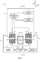
- FIG. 1 is a front isometric view illustrating a system for magnetic shielding in inductive power transfer.
- the system 100 may include a first electronic device 101 and a second electronic device 102.
- FIG. 1 illustrate the first electronic device 101 as a cordless electronic device of a particular shape and the second electronic device 102 as a dock for the cordless electronic device, it is understood that this is merely an example.
- either the first electronic device 101 or the second electronic device 102 may be any kind of electronic device such as a laptop computer, a tablet computer, a mobile computing device, a smart phone, a cellular telephone, a digital media player, a dock that connects to another electronic device for the purposes of charging and/or connecting the electronic device to one or more external components, and/or any other such electronic device.
- the first electronic device 101 includes a first connection surface 103 that is operable to contact a second connection surface 104 of the second electronic device 102.
- the first and second electronic devices 101, 102 may be positionable with respect to each other in at least lateral 199 and transverse 198 relative directions.
- FIG. 2 is a cross-sectional view of the system 100 of FIG. 1 taken along section A-A of FIG. 1 illustrating the first and second connectible electronic devices 101 and 102 in an aligned position.
- FIG. 3 illustrates the system of FIG. 2 showing the first and second connectible electronic devices 101 and 102 in one possible contact position.
- the first and second connection surfaces 103 and 104 may contact at any number of different points. As such, any number of different contact positions may be possible, of which FIG. 3 is an example.
- the first and second connectible electronic devices 101 and 102 may have a single aligned position, illustrated in FIG.
- FIG. 4 is a cross-sectional side view of the system of FIG. 2 taken along section B-B of FIG. 2 .
- the first electronic device 101 may include one or more first magnetic elements 105 (which may be a permanent magnet and may include a shield element 106), inductive power transfer receiving coil 107a and 107b (cross-sectional portions of a single coil that respectively include shield elements 140a and 140b), processing units 108, one or more non-transitory storage media 109 (which may take the form of, but is not limited to, a magnetic storage medium; optical storage medium; magneto-optical storage medium; read only memory; random access memory; erasable programmable memory; flash memory; and so on), and/or one or more power sources 110 (such as one or more batteries).
- first magnetic elements 105 which may be a permanent magnet and may include a shield element 106
- inductive power transfer receiving coil 107a and 107b cross-sectional portions of a single coil that respectively include shield elements 140a and 140b
- processing units 108 processing units 108
- one or more non-transitory storage media 109 which may take the form of, but is not limited to,
- the processing unit 108 may execute one or more instructions stored in the non-transitory storage medium 109 to perform one or more first electronic device operations such as one or more receiving operations utilizing the receiving component, communication operations, calculation operations, storage operations, input/output operations, time operations, charging operations, and so on.
- first electronic device operations such as one or more receiving operations utilizing the receiving component, communication operations, calculation operations, storage operations, input/output operations, time operations, charging operations, and so on.
- the second electronic device 102 may include one or more second magnetic elements 111 (which may be a permanent magnet and may include a shield element 112), inductive power transfer transmitting coil 113a and 113b (cross-sectional portions of a single coil that respectively include shield elements 141a and 141b), processing units 114, one or more non-transitory storage media 115, and/or one or more power sources 116 (such as one or more alternating current or direct current power sources).
- the processing unit 114 may execute one or more instructions stored in the non-transitory storage medium 115 to perform one or more second electronic device operations such as one or more transmitting operations utilizing the transmitting component, calculation operations, storage operations, and so on.
- the inductive power transfer transmitting coil 113a and 113b may be configured to inductively transmitting power to the inductive power transfer receiving coil 107a and 107b.
- the first magnetic element 105 may be positioned within the center, or along an axis (corresponding to the transverse direction 198 in this example implementation) running through the center, of the inductive power transfer receiving coil 107a and 107b.
- the second magnetic element 111 may be positioned within the center, or along an axis (corresponding to the transverse direction 198 in this example implementation) running through the center, of the inductive power transfer transmitting coil 113a and 113b.
- first and/or second magnetic elements and/or the inductive power transfer transmitting and/or receiving coils may be configured to minimize or reduce eddy currents caused in the first and/or second magnetic elements by the inductive power transfer transmitting and/or receiving coils.
- the first and/or second magnetic elements (105, 111) and/or the inductive power transfer transmitting and/or receiving coils (113a-b, 107a-b) may be configured to minimize or reduce eddy currents in a variety of different ways.
- the inductive power transfer transmitting coil 113a and 113b and the inductive power transfer receiving coil 107a and 107b may be inductively coupled in the aligned position.
- Transmitting and receiving coils in an inductive power transfer system may be inductively coupled when they are centered with respect to each other and sufficiently adjacent that the receiving coil is within the majority of the inductive current field generated by the transmitting coil.
- the inductive power transfer transmitting coil 113a and 113b, the inductive power transfer receiving coil 107a and 107b, and the first and second magnetic elements 105 and 111 may be spaced in relation to each other in order to minimize creation of eddy currents in the first and/or second magnetic elements. Positioning of either magnetic element too closely, such as immediately adjacent, to either coil may cause creation of eddy currents. However, spacing as illustrated may reduce the eddy currents that may otherwise be created by proximity of the magnetic elements and the coils.
- first and/or second connection surfaces 103 and 104 may be formed of one or more nonconductive materials. This may prevent formation of eddy currents in the connection surfaces and may further increase transmission efficiency and reduce generated heat.
- the first and second magnetic elements 105 and 111 may include shield elements 106 and 112, respectively.
- Each magnetic element may have a face surface and an opposite surface that are joined by at least two side surfaces wherein the face surface faces the respective connection surface.
- the respective shield element may at least partially cover the opposite surface and the two side surfaces.
- a gap 117 or 118 may be present between the respective shield element and the at least two side surfaces.
- Such shield elements may be formed of one or more electrically nonconductive materials, soft magnetic material, ferromagnetic material, ceramic materials, crystalline materials, iron cobalt, and/or other such materials.
- a soft magnetic material may be electrically conductive, such as a nonconductive ceramic material that includes ferrous metal fibers or particles suspended therein. As the fibers or particles are separated by nonconductive material, the combination may itself be nonconductive even though the presence of the ferrous metal fibers or particles may cause the combination to be a soft magnetic material.
- a shield element may be at least partially coated with a nonconductive coating such as those discussed in further detail below.
- the shield element 106 or 112 may be at least partially positioned between the first or second magnet 105 and 111 and the inductive power transfer transmitting coil 113a and 113b or the inductive power transfer receiving coil 107a and 107b, respectively.
- the gap 117 or 118 may be positioned between a surface of the respective magnetic element and the respective coil.
- the shield element 106 or 112 which may be formed of ferromagnetic material, a soft magnetic material, or other material that demonstrates the ability to easily become magnetic such as iron cobalt, may direct a magnetic field of the magnetic element in a direction of the connection surface. Such direction of the magnetic field may enable use of smaller magnetic elements than would otherwise be possible and may prevent the magnetic fields of the first and/or second magnetic elements 105 and 111 from interfering with (thus causing eddy currents in the magnetic elements) the inductive current field between the inductive power transfer transmitting coil 113a and 113b and the inductive power transfer receiving coil 107a and 107b.
- the shielding elements 106 and 112 are illustrated as having a single, solid structure, it is understood that this is an example.
- one or more of the shielding elements may be formed to have one or more "cutouts," or intermittent breaks in the material of the shield. Such cutouts may interrupt electrical conductivity through portions of such a shield and may further minimize the formation of eddy currents while still allowing for a highly permeable volume.
- FIG. 5A illustrates a magnetic field 120A of the first magnetic element 105 of FIG. 2 removed from the first electronic device 101 and the shield element 106.
- FIG. 5B illustrates the magnetic field 120A of the first magnetic element including the shield element of FIG. 2 removed from the first electronic device.
- the inclusion of the shield element may direct the magnetic field 120A toward the first connection surface (item 103 in FIGs. 2-4 ).
- FIGs. 5A and 5B illustrate the magnetic field 120A as circulating in one sample direction, it is understood that this is an example. In other embodiments, the magnetic field 120A may be reversed without departing from the scope of the present disclosure.
- the inductive power transfer transmitting coil 113a and 113b or the inductive power transfer receiving coil 107a and 107b may include shield elements 140a and 140b or 141a and 141b, respectively.
- Each coil may have a collective face surface and an collective opposite surface that are joined by at least two collective side surfaces wherein the collective face surface faces the respective connection surface.
- the respective shield element may at least partially cover the collective opposite surface and the collective two side surfaces.
- shield elements 140a and 140b or 141a and 141b may be at least partially positioned between the inductive power transfer transmitting coil 113a and 113b or the inductive power transfer receiving coil 107a and 107b and the first or second magnetic elements 105 and 111, respectively.
- These shield elements may function as a Faraday cage, blocking electromagnetic radiation. As such, these shield elements may block one or more of the magnetic elements from the inductive current field between the inductive power transfer transmitting coil and the inductive power transfer receiving coil, thus reducing eddy currents that may otherwise be caused in the magnetic elements.
- Such shield elements may be formed of one or more crystalline materials, ceramic materials, soft magnetic material, ferromagnetic materials, iron silicon, and/or other such materials.
- the shielding elements 140a and 140b or 141a and 141b are illustrated as having a single, solid structure, it is understood that this is an example.
- one or more of the shielding elements may be formed to have one or more "cutouts," or intermittent breaks in the material of the shield. Such cutouts may interrupt electrical conductivity through portions of such a shield and may further minimize the formation of eddy currents while still allowing for a highly permeable volume.
- one or more of the first and/or second magnetic elements 105 and 111 may be at least partially coated with one or more nonconductive coatings.
- FIG. 7 illustrates an example implementation that includes such nonconductive coatings 131 and 132.
- Such nonconductive coatings may reduce eddy currents that may otherwise be caused in the first and/or second magnetic element by the inductive power transfer transmitting coil 113a and 113b or the inductive power transfer receiving coil 107a and 107b.
- Such coatings may be formed of one or more nonconductive and/or magnetically permeable materials such as polyurethane, plastic, a combination of polyurethane and/or plastic and conductive fibers or particles, a combination of other nonconductive materials and conductive fibers or particles, and/or other such nonconductive and/or magnetically permeable materials.
- nonconductive and/or magnetically permeable materials such as polyurethane, plastic, a combination of polyurethane and/or plastic and conductive fibers or particles, a combination of other nonconductive materials and conductive fibers or particles, and/or other such nonconductive and/or magnetically permeable materials.
- the inductive power transfer receiving coil 107a and 107b is shown as being generally parallel to a top surface of the first electronic device 101 and the inductive power transfer transmitting coil 113a and 113b is shown as being generally parallel to a bottom surface of the second electronic device 102 such that they are not flush aligned with the first and second connection surfaces 103 and 104, it is understood that this is an example.
- the inductive power transfer receiving coil 107a and 107b may be flush with the first connection surface and the inductive power transfer transmitting coil 113a and 113b may be flush with the second connection surface without departing from the scope of the present disclosure.
- the inductive power transfer receiving coil 107a and 107b and the inductive power transfer transmitting coil 113a and 113b may be angled with respect to the top surface of the first electronic device and/or the bottom surface of the second electronic device.
- FIG. 6 is a method diagram illustrating a method 600 for magnetic shielding in inductive power transfer. This method may be performed, for example, by the system of FIG. 1 .
- the flow may begin at block 601 where an inductive power transfer receiving coil and first magnetic element of a first electronic device may be positioned adjacent to a connection surface of the first electronic device.
- the flow may then proceed to block 602 where the inductive power transfer receiving coil and the first magnetic element may be configured to minimize or reduce eddy currents caused in the first magnetic element by the inductive power transfer receiving coil.
- the first electronic device may be coupled or connected to a second electronic device utilizing the first magnetic element and the second magnetic element of the second electronic device.
- the flow may then proceed to block 604 where power may be inductively received utilizing inductive power transfer receiving coil from inductive power transfer transmitting coil of the second electronic device.
- block 602 is shown and described above as configuring the inductive power transfer receiving coil and the first magnetic element may to minimize or reduce eddy currents caused in the first magnetic element by the inductive power transfer receiving coil.
- either the inductive power transfer receiving coil or first magnetic element may be so configured.
- the inductive power transfer receiving and/or transmitting coils and/or the first and/or second magnetic elements may be configured to minimize or reduce eddy currents caused in either magnetic element caused by either of the coils without departing from the scope of the present disclosure.
- FIG. 8 a simplified block diagram of an example frequency controlled inductive charging system 800 is shown that may be utilized with inductive power transfer transmitting coil (e.g., 113a and 113b of FIGs. 2-4 ) and inductive power transfer receiving coil (e.g., 107a and 107b of FIGs. 2-4 ).
- the inductive charging system 800 includes a clock circuit 802 operatively connected to a controller 804 and a direct-current converter 806.
- the clock circuit 802 can generate the timing signals for the inductive charging system 800.
- the controller 804 may control the state of the direct-current converter 806.
- the clock circuit 802 generates periodic signals that are used by the controller 804 to activate and deactivate switches in the direct-current converter 806 on a per cycle basis.
- Any suitable direct-current converter 806 can be used in the inductive charging system 800.
- an H bridge may be used in the direct-current converter 806. H bridges are known in the art, so only a brief summary of the operation of an H bridge is described herein.
- the controller 804 controls the closing and opening of four switches S1, S2, S3, S4 (not illustrated).
- switches S1 and S4 When switches S1 and S4 are closed for a given period of time and switches S2 and S3 are open, current may flow from a positive terminal to a negative terminal through a load.
- switches S2 and S3 are closed for another given period of time while switches S1 and S4 are open, current flows from the negative terminal to the positive terminal.
- This opening and closing of the switches produces a time-varying current by repeatedly reversing the direction of the current through the load same load.
- an H bridge may not be required.
- a single switch may control the flow of current from the direct-current converter 806. In this manner, the direct-current converter 806 may function as a square wave generator.
- the time-varying signal or square wave signal produced by the direct-current converter 806 may be input into a transformer 808.
- a transformer such as those used in the above-referenced tethered charging systems includes a primary coil coupled to a secondary coil, with each coil wrapped about a common core.
- an inductive charging system as described herein includes a primary and a secondary coil separated by an air gap and the respective housings containing each coil.
- transformer 808 may not necessarily be a physical element but instead may refer to the relationship and interface between two inductively proximate electromagnetic coils such as a primary coil 810 (which may be the transmitting component 113a and 113b of the system 100 of FIG. 2 ) and a secondary coil 812 (which may be the receiving component 107a and 107b of the system 100 of FIG. 2 ).
- the transmitter may be configured to provide a time-varying voltage to the primary coil 810 in order to induce a voltage within the secondary coil 812.
- the controller 804 may control a plurality of states of the direct-current converter 806.
- the controller 804 may control the voltage, current, duty cycle, waveform, frequency, or any combination thereof.
- the controller 804 may periodically modify various characteristics of the waveforms applied to the primary coil 810 in order to increase the efficiency of the operation of the power transmitting circuitry. For example, in certain cases, the controller 804 may discontinue all power to the primary coil 810 if it is determined that the secondary coil 812 may not be inductively proximate the primary coil 810. This determination may be accomplished in any number of suitable ways. For example, the controller 804 may be configured to detect the inductive load on the primary coil 810. If the inductive load falls below a certain selected threshold, the controller 804 may conclude that the secondary coil 812 may not be inductively proximate the primary coil 810. In such a case, the controller 804 may discontinue all power to the primary coil 810.
- the controller 804 may set the duty cycle to be at or near a resonance frequency of the transformer 808.
- the period of the waveform defining the active state of the duty cycle i.e., high
- the controller 804 may set the duty cycle to be at or near the resonance frequency of the transformer 808.
- the controller 804 may discontinue all power to the primary coil 810 if a spike in inductive load is sensed. For example, if the inductive load spikes at a particular rate above a certain selected threshold the controller 804 may conclude that an intermediate object may be placed inductively proximate the primary coil 810. In such a case, the controller 804 may discontinue all power to the primary coil 810.
- the controller 804 may modify other characteristics of the waveforms applied to the primary coil 810. For example, if the receiver circuitry requires additional power, the controller 804 may increase the duty cycle of the waveform applied to the primary coil 810. In a related example, if the receiver circuitry requires less power, the controller 804 may decrease the duty cycle of the waveform applied to the primary coil 810. In each of these examples, the time average power applied to the primary coil 810 may be modified.
- the controller 804 may be configured to modify the magnitude of the waveform applied to the primary coil 810. In such an example, if the receiver circuitry requires additional power, the controller 804 may amplify the maximum voltage of the waveform applied to the primary coil 810. In the related case, the maximum voltage of the waveform may be reduced if the receiver circuitry requires less power.
- the transmitter portion of the inductive power transfer system may be configured to provide a time-varying signal to the primary coil 810 in order to induce a voltage within the secondary coil 812 in the receiver through inductive coupling between the primary coil 810 and the secondary coil 812. In this manner, power may be transferred from the primary coil 810 to the secondary coil 812 through the creation of a varying magnetic flux by the time-varying signal in the primary coil 810.
- the time-varying signal produced in the secondary coil 812 may be received by an direct-current converter 814 that converts the time-varying signal into a DC signal.
- Any suitable direct-current converter 814 can be used in the inductive charging system 800.
- a rectifier may be used as an direct-current converter.
- the DC signal may then be received by a programmable load 816.
- the receiver direct-current converter 814 may be a half bridge.
- the secondary coil 812 may have an increased number of windings.
- the secondary coil may have twice as many windings.
- the induced voltage across the secondary coil 812 may be reduced by half, effectively, by the half bridge rectifier.
- this configuration may require substantially fewer electronic components.
- a half bridge rectifier may require half as many transistors as a full wave bridge rectifier. As a result of fewer electronic components, resistive losses may be substantially reduced.
- the receiver may also include circuitry to tune out magnetizing inductance present within the transmitter.
- magnetizing inductance may result in losses within a transformer formed by imperfectly coupled coils. This magnetizing inductance, among other leakage inductance, may substantially reduce the efficiency of the transmitter.
- tuning circuitry may be included within the receiver. For example, in certain embodiments, a capacitor may be positioned parallel to the programmable load 816.
- a combination of the above-referenced sample modifications may be made by the controller.
- the controller 804 may double the voltage in addition to reducing the duty cycle.
- the controller may increase the voltage over time, while decreasing the duty cycle over time.
- Other embodiments may include multiple primary coils 810. For example, if two primary coils are present, each may be activated or used independently or simultaneously. In such an embodiment, the individual coils may each be coupled to the controller 804. In further examples, one of the several individual primary coils 810 may be selectively shorted. For example, a switch may be positioned in parallel to the coil such that when the switch is off current may run through the inductor. On the other hand, when the switch is on, no current will run through the coil. The switch may be any suitable type of manual, solid state, or relay based switch. In this manner, the amount of increase in current through each of the several coils may be electively controlled. For example, in a circumstance with a high inductive load, the switch may be turned off to include the coil in the circuit with the primary coil 810.
- FIG. 9 is a simplified isometric view of an inductive power transmission system 900 in accordance with another embodiment from which a number of components have been omitted for purposes of clarity.
- a first electronic device 901 may be operable to receive power inductively transmitted from a second electronic device 902; the first electronic device may store the power in one or more batteries (not shown).
- the first electronic device may include a housing 903 and the second electronic device may include a housing 904.
- the first electronic device 901 is illustrated as a smart phone and the second electronic device 902 is illustrated as a charging dock for the smart phone. However, it is understood that this is an example. In various implementations the first and/or second electronic devices may be any kind of electronic devices. Further, although the first electronic device 901 is described as receiving power inductively transmitted from the second electronic device 902, it is understood that this is an example and that other transmission configurations may be utilized without departing from the scope of the present disclosure.
- FIG. 10A is a cross-sectional side view of a first implementation of the inductive power transmission system 900 of FIG. 9 , taken along the section C-C of FIG. 9 .
- the first electronic device 901 may include an inductive receive coil 907 and an alignment magnet 905.
- the second electronic device 902 may include an inductive transmit coil 908 and an alignment magnet 906.
- the alignment magnets 905 and 906 may be operable to assist in aligning the inductive transmit and receive coils for inductive power transmission and to keep the coils aligned during transmission.
- magnetic flux 1001a may be generated by and flow through the inductive transmit and receive coils 907 and 908 during inductive power transmission.
- Such magnetic flux 1001 may interact with the housing 903 and/or the housing 904. This interaction may cause eddy currents to form in the housing 903 and/or the housing 904. Such eddy currents may cause efficiency losses in the inductive power transmission and/or may increase the temperature of one or more portions of the housing 903 and/or the housing 904.
- FIG. 10B is a cross-sectional side view of a second implementation of the inductive power transmission system 900 of FIG. 9 , taken along the section C-C of FIG. 9 .
- one or more magnetic field directing materials 909a, 909b, 910a, and 910b or shields may be positioned between the inductive receive coil 907 and the housing 903 and/or the inductive transmit coil 908 and the housing 904. These magnetic field directing materials may block or direct the magnetic flux 1001b from portions of the respective housings.
- the magnetic field directing materials 909a, 909b, 910a, and 910b may shape the magnetic flux 1001b to block the magnetic flux from the sides of the respective housings 903 and 904. This may reduce interaction between the magnetic flux and the side portions of the housing, thereby reducing or preventing the formation of eddy currents in the side portions, efficiency losses in the inductive power transmission, and/or increases in temperature at the side portions.
- the magnetic field directing materials 909a, 909b, 910a, and 910b may be formed of a diamagnetic material.
- a diamagnetic material is a material that creates a magnetic field in opposition to an externally applied magnetic field, thus causing a repulsive effect.
- Such diamagnetic materials may include graphite, bismuth, graphene, pyrolytic carbon, and so on.
- the magnetic field directing materials 909a, 909b, 910a, and 910b may be formed of a superconductive material.
- a superconductive material is a material that exhibits zero electrical resistance and expels magnetic fields when cooled below a characteristic critical temperature.
- Such superconductive materials may include a lanthanum-based cuprate perovskite material, yttrium barium copper oxide, lanthanum oxygen fluorine iron arsenide, and so on.
- the magnetic field directing materials 909a, 909b, 910a, and 910b are formed of a relatively highly thermally conductive material such as graphite
- the magnetic field directing materials may operate as a heat spreader.
- the magnetic field directing materials may dissipate heat generated by the inductive power transmission and/or from other heat generation sources (such as heat generated by power dissipating components, solar loading, and so on).
- the magnetic field directing materials 909a, 909b, 910a, and 910b operate as a heat spreader
- the magnetic field directing materials may be configured to optimize their heat dissipation properties.
- the amount of heat that the magnetic field directing materials are able to dissipate in a particular period of time may be related to the surface area of the magnetic field directing materials, the thickness of the magnetic field directing materials, and/or other such factors.
- the magnetic field directing materials 909a, 909b, 910a, and 910b may be configured to increase length (shown vertically in FIG. 10B ) and/or width (not shown in FIG. 10B as FIG. 10B is a cross sectional view) with respect to thickness (shown horizontally in FIG. 10B ) such that the magnetic field directing materials have a large surface area in relation to the amount of material, in order to increase heat dissipation and reduce the time required to dissipate heat while still blocking the magnetic flux 1001b from as much of the housings 903 and/or 904 as possible.
- the magnetic field directing materials 909a, 909b, 910a, and 910b may form one or more projections, such as fins or extensions, in order to increase the surface area of the magnetic field directing materials beyond that occupied by the length and width of the materials.
- projections may enable the magnetic field directing materials to dissipate more heat in a shorter amount of time than embodiments without such structures, and without altering the housings 903 and/or 904 shielded from the magnetic flux 1001b.
- the magnetic field directing materials 909a, 909b may be positioned between one or more surfaces of the inductive receive coil 907 and one or more internal portions of the housing 903. As similarly illustrated, the magnetic field directing materials 910a and 910b may be positioned between one or more surfaces of the inductive transmit coil 908 and one or more internal portions of the housing 904. However, it is understood that this is an example. In various implementations, magnetic field directing material may be positioned between inductive coils and internal housing portions, located within housings, and/or located on one or more external housing surfaces.
- the housings 903 and/or 904 themselves may be formed of magnetic field directing materials (such as diamagnetic materials and/or superconductive materials).
- the housings may be formed of paramagnetic materials, combinations of magnetic field directing materials and paramagnetic materials (materials are attracted by an externally applied magnetic field), conductive materials, and/or any other materials.
- the magnetic field directing materials 909a, 909b, 910a, and 910b are positioned on both internal sides of both housings 903 and 904. However, it is understood that this is an example. In various implementations, any number, or amount, of magnetic field directing materials may be variously positioned without departing from the scope of the present disclosure.
- the first electronic device 901 may include the magnetic field directing materials 909a and 909b whereas the magnetic field directing materials 910a and 910b may be omitted from the second electronic device 902.
- the first electronic device may include the magnetic field directing materials 909b but omit the magnetic field directing material 909a and the second electronic device may include the magnetic field directing material 910b but omit the magnetic field directing material 910a.
- magnetic field directing material may be included on just one side/region of the first and/or second electronic device 901 and 902, on a top internal surface of the housing 903 and/04 904, and so on.
- Various configurations are possible and contemplated.
- the first electronic device 901 and/or the second electronic device 902 may include magnetic field directing material in addition to the magnetic field directing materials 909a, 909b, 910a, and 910b.
- the additional magnetic field directing material may be positioned within and/or on one or more external surfaces of the housings 903 and/or 904.
- FIG. 10C is a cross-sectional side view of a third implementation of the inductive power transmission system 900 of FIG. 9 , taken along the section C-C of FIG. 9 .
- the magnetic field directing material 909c may surround all surfaces of the inductive receive coil 907 other than the surface facing the magnetic path toward the inductive transmit coil 908.
- the magnetic field directing material 910c may surround all surfaces of the inductive transmit coil other than the surface facing the magnetic path toward the inductive receive coil.
- the magnetic field directing materials 909c and 910c may shape the magnetic flux 1001c to block the magnetic flux 1001c from all surfaces of the housings 903 and 904 that are not in the magnetic path of the inductive power transmission.
- FIGs. 10A-10C illustrate the magnetic fields 100a-1000c as circulating in one sample direction, it is understood that this is an example. In other embodiments, one or more of the magnetic fields 100a-1000c may be reversed without departing from the scope of the present disclosure.
- FIG. 11 is a method diagram illustrating an example method 1100 for manufacturing an inductive power transmission system. This example method may be performed by the systems of FIGs. 9 , 10B , and/or 10C.
- an inductive coil of an electronic device may be configured for use in an inductive power transmission system.
- the inductive coil may be a transmit coil and/or a receive coil.
- configuring the inductive coil for use in an inductive power transmission system may include configuring the inductive coil to inductively transmit and/or receive power.
- configuring the inductive coil for use in an inductive power transmission system may include configuring the inductive coil to inductively transmit and/or receive power from another inductive coil.
- a magnetic field directing mechanism is positioned to block magnetic flux of the inductive power transmission system from a housing of the electronic device.
- a magnetic field directing mechanism may include materials such as diamagnetic materials, superconductive materials, and so on that are operable block the magnetic flux.
- block 1102 is illustrated and described as positioning a magnetic field directing mechanism to block magnetic flux of the inductive power transmission system from a housing of the electronic device.
- the interaction between the magnetic flux and the housing portion may be reduced as opposed to entirely blocked without departing from the scope of the present disclosure.
- Such reducing of the interaction between the magnetic flux and the housing portion may be performed utilizing materials such as diamagnetic materials, superconductive materials, and so on.
- an additional operation of configuring the magnetic field directing mechanism to dissipate heat as a heat spreader may be performed without departing from the scope of the present disclosure.
- Such heat may be generated by the inductive power transmission and/or by other factors such as heat generated by power dissipating components, solar loading, and so on.
- FIGs. 1-11 are discussed in the context of various embodiments, it is understood that these are examples. In various implementations, various features of various different discussed embodiments may be utilized together without departing from the scope of the present disclosure.
- FIGs. 12-14 illustrate isometric views of sample electronic devices 1201-1401 in which various embodiments of the magnetic connection and alignment techniques disclosed herein may be utilized.
- FIG. 12 illustrates a smart phone 1201
- FIG. 13 illustrates a tablet computer 1301
- FIG. 14 illustrates a wearable device 1401.
- FIG. 12 illustrates a smart phone 1201
- FIG. 13 illustrates a tablet computer 1301
- FIG. 14 illustrates a wearable device 1401.
- FIG. 12 illustrates a smart phone 1201
- FIG. 13 illustrates a tablet computer 1301
- FIG. 14 illustrates a wearable device 1401.
- FIG. 12 illustrates a smart phone 1201
- FIG. 13 illustrates a tablet computer 1301
- FIG. 14 illustrates a wearable device 1401.
- FIGs. 1-11 illustrate various configurations of components (such as inductive power receiving coil 107a and 107b, inductive power transmitting coil 113a and 113b, and magnetic elements 105 and 111), it is understood that these are examples. Various other configurations are possible in various implementations without departing from the scope of the present disclosure.
- FIG. 15 is a schematic cross sectional side view of the wearable device 1401 of FIG. 14 , taken along section D-D of FIG. 14 , illustrating another sample configuration of inductive power receiving coil 1407a and 1407b, first magnetic element 1405, first connection surface 1403, shield elements 1440a and 1440b, and shield element 1406.
- this configuration is also an example and that still other configurations are possible without departing from the scope of the present disclosure.
- one or more magnetic field directing materials such as the magnetic field directing materials 909a, 909b, and/or 909c of FIGs. 10A-10C may be positioned on various portions of and/or inside the housing of the wearable device 1401 without departing from the scope of the present disclosure.
- a first electronic device with a first connection surface and an inductive power transfer receiving coil and first magnetic element positioned adjacent to the first connection surface connects in an aligned position with a second electronic device with a second connection surface and an inductive power transfer transmitting coil and second magnetic element positioned adjacent to the second connection surface.
- the aligned position the relative position of first and second electronic devices may be maintained by magnetic coupling between the first and second magnetic elements.
- the inductive power transfer transmitting coil may be configured to transmit power to the inductive power transfer receiving coil.
- the first and/or second magnetic elements and/or the inductive power transfer receiving and/or transmitting coils may be configured to minimize or reduce eddy currents caused in the first and/or second magnetic elements by the inductive power transfer receiving and/or transmitting coils. In this way, magnetic connection mechanisms may be utilized without impairing the inductive power transfer and/or causing excessive heat.
- the methods disclosed may be implemented utilizing sets of instructions or software readable by a device. Further, it is understood that the specific order or hierarchy of steps in the methods disclosed are examples of sample approaches. In other embodiments, the specific order or hierarchy of steps in the method can be rearranged while remaining within the disclosed subject matter.
- the accompanying method claims present elements of the various steps in a sample order, and are not necessarily meant to be limited to the specific order or hierarchy presented.
- the described disclosure may utilize a computer program product, or software, that may include a non-transitory machine-readable medium having stored thereon instructions, which may be used to program a computer system (such as a computer controlled manufacturing system and/or other electronic devices) to perform a process utilizing techniques of the present disclosure.
- a non-transitory machine-readable medium includes any mechanism for storing information in a form (e.g., software, processing application) readable by a machine (e.g., a computer).
- the non-transitory machine-readable medium may take the form of, but is not limited to, a magnetic storage medium (e.g., floppy diskette, video cassette, and so on); optical storage medium (e.g., CD-ROM); magneto-optical storage medium; read only memory (ROM); random access memory (RAM); erasable programmable memory (e.g., EPROM and EEPROM); flash memory; and so on.
- a magnetic storage medium e.g., floppy diskette, video cassette, and so on
- optical storage medium e.g., CD-ROM
- magneto-optical storage medium e.g., magneto-optical storage medium
- ROM read only memory
- RAM random access memory
- EPROM and EEPROM erasable programmable memory
- flash memory and so on.
- a first electronic device comprising: a first connection surface; an inductive power transfer receiving coil positioned adjacent to the first connection surface; a first magnetic element positioned adjacent to the first connection surface; and a shield at least partially positioned between the inductive power transfer receiving coil and the first magnetic element; wherein: the shield is configured to reduce an eddy current caused in the first magnetic element by the inductive power transfer receiving coil; the first magnetic element couples to a second magnetic element of a second electronic device to maintain an aligned position between the first and second electronic devices; and the inductive power transfer receiving coil is configured to inductively receive power from an inductive power transfer transmitting coil of the second electronic device when the first electronic device and the second electronic device are in the aligned position.
- the nonconductive and magnetically permeable coating is formed of at least one of polymer, a combination of the polymer and conductive fibers, or a combination of the polymer and conductive particles.
- the shield is coupled to the first magnetic element.
- the portion of the shield positioned between the first magnetic element and the inductive power transfer receiving coil defines a gap between the shield and the first magnetic element.
- the shield is formed of at least one of an electrically nonconductive material, a soft magnetic material, a ferromagnetic material, a ceramic material, a crystalline material, or iron cobalt.
- the shield directs a magnetic field of the first magnetic element toward the first connection surface.
- the shield is coated with a nonconductive coating.
- a spacing between the first magnetic element and the inductive power transfer receiving coil is configured to reduce the eddy current.
- a system for magnetic shielding for an inductive power transfer comprising: a first electronic device, comprising: a first connection surface; an inductive power transfer receiving coil positioned adjacent to the first connection surface; and a first magnetic element positioned adjacent to the first connection surface; and a second electronic device, comprising: a second connection surface; an inductive power transfer transmitting coil positioned adjacent to the second connection surface; and a second magnetic element positioned adjacent to the second connection surface; wherein: the inductive power transmitting coil inductively transmits power to the inductive power transfer receiving coil; and at least one of first magnetic element or the inductive power transfer receiving coil includes a shield that is configured to reduce an eddy current caused in the first magnetic element as a result of inductively transmitting power to the inductive power receiving coil.
- the shield is coupled to the inductive power transfer receiving coil and is configured to reduce the eddy current.
- the shield is a Faraday cage.
- the shield is formed of at least one of a crystalline material, a ceramic material, a soft magnetic material, a ferromagnetic material, or an iron silicon.
- the shield is at least partially positioned between the inductive power transfer receiving coil and the first magnetic element.
- the first connection surface is formed of a nonconductive material.
- At least one of: at least one of the second magnetic element or the inductive power transfer receiving coil is configured to reduce eddy currents caused in the second magnetic element by the inductive power transfer receiving coil; or at least one of the first magnetic element or the inductive power transfer transmitting coil is configured to reduce eddy currents caused in the first magnetic element by the inductive power transfer transmitting coil.
- an electronic device comprising: a housing; an inductive coil located within the housing and operable to transmit or receive power in an inductive power transmission system; and a magnetic field directing material positioned either within or on the housing; wherein the magnetic field directing material blocks magnetic flux of the inductive power transmission system from the housing.
- the magnetic field directing material comprises at least one of a diamagnetic material or a superconductive material.
- the diamagnetic material comprises at least one of graphite, bismuth, graphene, or pyrolytic carbon.
- the magnetic field directing material is positioned between the inductive coil and the housing.
- the magnetic field directing material is positioned on an interior surface of the housing.
- the housing including the magnetic field directing material.
- the magnetic field directing material comprises a thermally conductive material.
- the thermally conductive material is configured to operate as a heat spreader.
- the housing comprises at least one of a paramagnetic material or a diamagnetic material.
- the magnetic field directing material is positioned between multiple surfaces of the inductive coil and the housing.
- the magnetic field directing material surrounds all surfaces of the inductive coil other than a surface of the inductive coil facing a magnetic path of the inductive power transmission system.
- the magnetic field directing material is configured to shape a flow of the magnetic flux.
- the magnetic field directing material is configured to prevent formation of eddy currents in the housing.
- the magnetic field directing material is configured to reduce efficiency losses of the inductive power transmission system.
Abstract
Description
- This Patent Cooperation Treaty patent application claims priority to
U.S. Provisional Patent Application No. 61/969,337, filed March 24, 2014 U.S. Provisional Patent Application No. 62/036,685, filed August 13, 2014 - This disclosure relates generally to connectible devices, and more specifically to magnetic shielding in inductive power transfer between connectible devices.
- Many electronic devices connect to other electronic devices. For example, electronic devices such as portable digital media players, wearable devices, and/or other kinds of portable computing devices may connect to one or more docks in order to charge, transfer data, connect to one or more accessories, such as external input/output devices, and so on. A connection may mechanically couple the electronic devices and/or may electrically couple the electronic devices for the purposes of power and/or data transmission. Using some traditional coupling techniques, it may be difficult to maintain a mechanical coupling between the electronic devices in a way that does not interfere or further facilitates an electrical coupling between the electronic devices.
- The present disclosure includes systems and methods for magnetic shielding in an inductive power transfer system. A first electronic device with a first connection surface and an inductive power transfer receiving coil and first magnetic element positioned adjacent to the first connection surface connects in an aligned position with a second electronic device with a second connection surface and an inductive power transfer transmitting coil and second magnetic element positioned adjacent to the second connection surface. In the aligned position, the first and second electronic devices may be coupled by the first and second magnetic elements and the inductive power transfer transmitting coil may be configured to transmit power to the inductive power transfer receiving coil. The first and/or second magnetic elements and/or the inductive power transfer receiving and/or transmitting coils may be configured to minimize or reduce eddy currents caused in the first and/or second magnetic elements by the inductive power transfer receiving and/or transmitting coils.
- The first and/or second magnetic elements and/or the inductive power transfer receiving and/or transmitting coils may be configured in one or more of a variety of different ways to minimize or reduce eddy currents caused in the first and/or second magnetic elements by the inductive power transfer receiving and/or transmitting coils. In some implementations, the inductive power transfer receiving and/or transmitting coils may be inductively coupled in the aligned position. In various implementations, the positioning of the first and/or second magnetic elements and/or the inductive power transfer receiving and/or transmitting coils may be spaced so as to minimize or reduce eddy currents caused in the first and/or second magnetic elements. In one or more implementations, the first and/or second connection surfaces may be formed of one or more nonconductive materials.
- In some implementations, the first and/or second magnetic elements may be coated with one or more coatings. Such coatings may be formed of one or more nonconductive and/or magnetically permeable materials. Similarly, the first and/or second magnetic elements may be at least partially covered by one or more shield elements. Such shield elements may be formed of one or more electrically nonconductive materials. The inductive power transfer receiving and/or transmitting coils may also be at least partially covered by one or more shield elements. Such shield elements may be, or function as, a Faraday cage for the inductive power transfer receiving and/or transmitting coils.
- In other embodiments, an electronic device may include an inductive coil operable to participate in an inductive power transmission system and a housing or other enclosure. The electronic device may also include one or more magnetic field directing materials (such as diamagnetic material and/or superconductive material) that block magnetic flux of the inductive power transmission from a portion of the housing and/or otherwise shape the flow of the magnetic flux. The magnetic field directing material may also be highly thermally conductive and may operate as a heat spreader. In this way, loss efficiency of the inductive power transmission system may be improved. Temperature increase of the housing may also be prevented and/or mitigated.
- In various embodiments, a system for magnetic shielding in inductive power transfer includes a first electronic device and a second electronic device. The first electronic device includes a first connection surface, an inductive power transfer receiving coil positioned adjacent to the first connection surface, and a first magnetic element positioned adjacent to the first connection surface. At least one of the first magnetic element or the inductive power transfer receiving coil is configured to minimize or reduce eddy currents caused in the first magnetic element by the inductive power transfer receiving coil. The second electronic device includes a second connection surface, an inductive power transfer transmitting coil positioned adjacent to the second connection surface, and a second magnetic element positioned adjacent to the second connection surface. The first magnetic element and the second magnetic element connect the first electronic device and the second electronic device in an aligned position and the inductive power transfer transmitting coil is configured to inductively transmit power to the inductive power transfer receiving coil when the first electronic device and the second electronic device are in the aligned position.
- In some embodiments, an electronic device includes a first connection surface, an inductive power transfer receiving coil positioned adjacent to the first connection surface, and a first magnetic element positioned adjacent to the first connection surface. At least one of the first magnetic element or the inductive power transfer receiving coil is configured to minimize or reduce eddy currents caused in the first magnetic element by the inductive power transfer receiving coil. The first magnetic element connects the first electronic device to a second magnetic element of a second electronic device in an aligned position. The inductive power transfer receiving coil is configured to inductively receive power from an inductive power transfer transmitting coil of the second electronic device when the first electronic device and the second electronic device are in the aligned position.
- In one or more embodiments, an electronic device may include a housing, an inductive coil operable to participate in an inductive power transmission system, and a magnetic field directing material. The magnetic field directing material may block magnetic flux of the inductive power transmission system from a portion of the housing.
- It is to be understood that both the foregoing general description and the following detailed description are for purposes of example and explanation and do not necessarily limit the present disclosure. The accompanying drawings, which are incorporated in and constitute a part of the specification, illustrate subject matter of the disclosure. Together, the descriptions and the drawings serve to explain the principles of the disclosure.
-
-
FIG. 1 is a front isometric view illustrating a system for magnetic shielding in inductive power transfer. -
FIG. 2 is a cross-sectional view of the system ofFIG. 1 taken along section A-A ofFIG. 1 illustrating the connectible electronic devices in an aligned position. -
FIG. 3 illustrates the system ofFIG. 2 showing the connectible electronic devices in one possible contact position. -
FIG. 4 is a cross sectional side view of the system ofFIG. 2 taken along section B-B ofFIG. 2 . -
FIG. 5A illustrates a magnetic field of the first magnetic element ofFIG. 2 removed from the first electronic device and the shield element. -
FIG. 5B illustrates the magnetic field of the first magnetic element including the shield element ofFIG. 2 removed from the first electronic device. -
FIG. 6 is a method diagram illustrating a method for magnetic shielding in inductive power transfer. This method may be performed by the system ofFIG. 1 . -
FIG. 7 is a close up view of the first and second magnetic elements of an alternative embodiment of the first and second electronic devices in the aligned position. -
FIG. 8 is a simplified block diagram of an example frequency controlled inductive charging system. The example frequency controlled inductive charging system may be utilized with the system ofFIG. 2 . -
FIG. 9 is a simplified isometric view of an inductive power transmission system in accordance with another embodiment from which a number of components have been omitted for purposes of clarity. -
FIG. 10A is a cross-sectional side view of a first implementation of the inductive power transmission system ofFIG. 9 , taken along the section C-C ofFIG. 9 . -
FIG. 10B is a cross-sectional side view of a second implementation of the inductive power transmission system ofFIG. 9 , taken along the section C-C ofFIG. 9 . -
FIG. 10C is a cross-sectional side view of a third implementation of the inductive power transmission system of FIG.FIG. 9 , taken along the section C-C ofFIG. 9 . -
FIG. 11 is a method diagram illustrating an example method for manufacturing an inductive power transmission system. This example method may be performed by the systems ofFIGs. 9 ,10B , and/or 10C. -
FIGs. 12-14 illustrate isometric views of sample electronic devices in which various embodiments of the magnetic shielding techniques disclosed herein may be utilized. -
FIG. 15 is a schematic cross sectional side view of the wearable device ofFIG. 14 , taken along section D-D ofFIG. 14 . - The description that follows includes sample systems, methods, and apparatuses that embody various elements of the present disclosure. However, it should be understood that the described disclosure may be practiced in a variety of forms in addition to those described herein.
- The present disclosure includes systems and methods for magnetic shielding in inductive power transfer. In some embodiments, a first electronic device is coupled or connected in an aligned position with a second electronic device. The first electronic device may include inductive power transfer receiving coil and a first magnetic element, both positioned adjacent to the first connection surface. Similarly, a second electronic device may include an inductive power transfer transmitting coil and a second magnetic element, both positioned adjacent to the second connection surface. In the aligned position, the first and second electronic devices may be coupled or connected by the first and second magnetic elements (which may be permanent magnets) and the inductive power transfer transmitting coil may be configured to transmit power to the inductive power transfer receiving coil. The first and/or second magnetic elements and/or the inductive power transfer receiving and/or transmitting coils may be configured to minimize or reduce eddy currents caused in the first and/or second magnetic elements by the inductive power transfer receiving and/or transmitting coils. In this way, magnetic connection mechanisms may be utilized without impairing the inductive power transfer and/or causing excessive heat.
- The first and/or second magnetic elements and/or the inductive power transfer receiving and/or transmitting coils may be configured in one or more of a variety of different ways to minimize or reduce eddy currents caused in the first and/or second magnetic elements by the inductive power transfer receiving and/or transmitting coils. In some implementations, the inductive power transfer receiving and/or transmitting coils may be inductively coupled in the aligned position. In various implementations, the positioning of the first and/or second magnetic elements and/or the inductive power transfer receiving and/or transmitting coils may be spaced so as to minimize or reduce eddy currents caused in the first and/or second magnetic elements. In one or more implementations, the first and/or second connection surfaces may be formed of one or more nonconductive materials.
- In some implementations, the first and/or second magnetic elements may be coated with one or more coatings. Such coatings may be formed of one or more nonconductive and/or magnetically permeable materials such as a polymer including a polyurethane or other type of plastic. The coating may include a combination of a polymer and conductive fibers or particles, a combination of other nonconductive materials and conductive fibers or particles, and/or other such nonconductive and/or magnetically permeable materials.
- Similarly, the first and/or second magnetic elements may be at least partially covered by one or more shield elements. Such shield elements may be formed of one or more electrically nonconductive materials, soft magnetic material, ferromagnetic material, ceramic materials, crystalline materials, iron cobalt, and/or other such materials. In some cases, the shield element may be at least partially positioned between the first and/or second magnetic elements and the inductive power transfer receiving and/or transmitting coils, respectively. One or more gaps may be positioned between a surface of the first and/or second magnetic elements that faces the inductive power transfer receiving and/or transmitting coils, respectively, and the portion of the shield element positioned between. Such a shield element may direct a magnetic field of the first and/or second magnetic elements toward the respective connection surface. In some cases, the shield element may be at least partially covered by a nonconductive coating.
- The inductive power transfer receiving and/or transmitting coils may also be at least partially covered by one or more shield elements. Such shield elements may be formed of one or more crystalline materials, ceramic materials, soft magnetic material, ferromagnetic material, iron silicon, and/or other such materials and/or may function as a Faraday cage for the inductive power transfer receiving and/or transmitting coils. Such shield elements may be at least partially positioned between the inductive power transfer receiving and/or transmitting coils and the first and/or second magnetic elements, respectively.
- In various cases, the first and/or second magnetic elements may be positioned in the center of the inductive power transfer receiving and/or transmitting coils, respectively, and/or along an axis running through the center of the inductive power transfer receiving and/or transmitting coils.
- In other embodiment, an electronic device may include an inductive coil operable to participate in an inductive power transmission system, a housing or other enclosure, and one or more magnetic field directing materials. The magnetic field directing material may block magnetic flux of the inductive power transmission system from a portion of the housing, shaping the flow of the magnetic flux. In this way, loss efficiency of the inductive power transmission system may be improved and/or temperature increase of the housing may be prevented and/or mitigated.
- As used herein, a "lateral magnetic force" may be used to refer to a magnetic force that moves one or both of the devices in a lateral or an X- or a Y-direction with respect to one another. In some cases, the lateral magnetic force may refer to a resistance to a shear or lateral force between the devices. In some cases, some Z-direction (height) motion may occur as a byproduct of an alignment of the adjacent surfaces with respect to each other, particularly if the adjacent surfaces are curved. Lateral magnetic force is more fully discussed with respect to
FIGs. 1-3 below. As used herein, a "transverse magnetic force" refers to a magnetic force that attracts the devices toward each other in a transverse or Z-direction, which may operate to center and align the two devices as well as resist a separation or expansion of a gap between the two devices. Transverse magnetic force is more fully discussed with respect toFIGs. 1-3 below. As discussed herein, lateral magnetic force and transverse magnetic force may be components of the same, single magnetic field. Both may vary based on the positions of the magnetic elements. -
FIG. 1 is a front isometric view illustrating a system for magnetic shielding in inductive power transfer. Thesystem 100 may include a firstelectronic device 101 and a secondelectronic device 102. AlthoughFIG. 1 illustrate the firstelectronic device 101 as a cordless electronic device of a particular shape and the secondelectronic device 102 as a dock for the cordless electronic device, it is understood that this is merely an example. In various implementations, either the firstelectronic device 101 or the secondelectronic device 102 may be any kind of electronic device such as a laptop computer, a tablet computer, a mobile computing device, a smart phone, a cellular telephone, a digital media player, a dock that connects to another electronic device for the purposes of charging and/or connecting the electronic device to one or more external components, and/or any other such electronic device. - As illustrated in
FIG. 1 , the firstelectronic device 101 includes afirst connection surface 103 that is operable to contact asecond connection surface 104 of the secondelectronic device 102. As such, the first and secondelectronic devices -
FIG. 2 is a cross-sectional view of thesystem 100 ofFIG. 1 taken along section A-A ofFIG. 1 illustrating the first and second connectibleelectronic devices FIG. 3 illustrates the system ofFIG. 2 showing the first and second connectibleelectronic devices FIG. 3 is an example. However, the first and second connectibleelectronic devices FIG. 2 , where a firstmagnetic element 105 connects with a secondmagnetic element 111 and an inductive powertransfer transmitting coil transfer receiving coil electronic devices electronic device 102 functions as a charging dock for the firstelectronic device 101 by inductively transmitting power to the firstelectronic device 101, which the firstelectronic device 101 stores in thepower source 110.FIG. 4 is a cross-sectional side view of the system ofFIG. 2 taken along section B-B ofFIG. 2 . - As illustrated in
FIG. 2 , the firstelectronic device 101 may include one or more first magnetic elements 105 (which may be a permanent magnet and may include a shield element 106), inductive powertransfer receiving coil shield elements processing units 108, one or more non-transitory storage media 109 (which may take the form of, but is not limited to, a magnetic storage medium; optical storage medium; magneto-optical storage medium; read only memory; random access memory; erasable programmable memory; flash memory; and so on), and/or one or more power sources 110 (such as one or more batteries). Theprocessing unit 108 may execute one or more instructions stored in thenon-transitory storage medium 109 to perform one or more first electronic device operations such as one or more receiving operations utilizing the receiving component, communication operations, calculation operations, storage operations, input/output operations, time operations, charging operations, and so on. - Similarly, the second
electronic device 102 may include one or more second magnetic elements 111 (which may be a permanent magnet and may include a shield element 112), inductive powertransfer transmitting coil shield elements processing units 114, one or morenon-transitory storage media 115, and/or one or more power sources 116 (such as one or more alternating current or direct current power sources). Theprocessing unit 114 may execute one or more instructions stored in thenon-transitory storage medium 115 to perform one or more second electronic device operations such as one or more transmitting operations utilizing the transmitting component, calculation operations, storage operations, and so on. - When the first and second
electronic devices FIG. 3 ), lateral 199 magnetic force between the first and secondmagnetic elements FIG. 2 ) where transverse 198 magnetic force between the first and second magnetic elements may connect the two devices. In the aligned position, the inductive powertransfer transmitting coil transfer receiving coil - As illustrated in
FIG. 2 , the firstmagnetic element 105 may be positioned within the center, or along an axis (corresponding to thetransverse direction 198 in this example implementation) running through the center, of the inductive powertransfer receiving coil magnetic element 111 may be positioned within the center, or along an axis (corresponding to thetransverse direction 198 in this example implementation) running through the center, of the inductive powertransfer transmitting coil - When conductive materials, such as magnetic elements, are positioned within the induction field of a transmitting coil and receiving coil of an inductive power transfer system, eddy currents may be formed in the conductive materials. Such eddy currents may result in less current being received by the receiving coil, thus less inductive power transfer system efficiency. Such eddy currents may also cause undesired heating in the conductive materials. As such, the first and/or second magnetic elements and/or the inductive power transfer transmitting and/or receiving coils may be configured to minimize or reduce eddy currents caused in the first and/or second magnetic elements by the inductive power transfer transmitting and/or receiving coils.
- The first and/or second magnetic elements (105, 111) and/or the inductive power transfer transmitting and/or receiving coils (113a-b, 107a-b) may be configured to minimize or reduce eddy currents in a variety of different ways. As illustrated, the inductive power
transfer transmitting coil transfer receiving coil - As also illustrated in
FIG. 2 , the inductive powertransfer transmitting coil transfer receiving coil magnetic elements - In various implementations, the first and/or second connection surfaces 103 and 104 may be formed of one or more nonconductive materials. This may prevent formation of eddy currents in the connection surfaces and may further increase transmission efficiency and reduce generated heat.
- In some implementations, the first and second
magnetic elements shield elements gap - Such shield elements may be formed of one or more electrically nonconductive materials, soft magnetic material, ferromagnetic material, ceramic materials, crystalline materials, iron cobalt, and/or other such materials. In some cases, a soft magnetic material may be electrically conductive, such as a nonconductive ceramic material that includes ferrous metal fibers or particles suspended therein. As the fibers or particles are separated by nonconductive material, the combination may itself be nonconductive even though the presence of the ferrous metal fibers or particles may cause the combination to be a soft magnetic material. In various cases, whether formed of a conductive material, nonconductive material, or a combination thereof, such a shield element may be at least partially coated with a nonconductive coating such as those discussed in further detail below.
- The
shield element second magnet transfer transmitting coil transfer receiving coil gap - The
shield element magnetic elements transfer transmitting coil transfer receiving coil - Although the shielding
elements -
FIG. 5A illustrates amagnetic field 120A of the firstmagnetic element 105 ofFIG. 2 removed from the firstelectronic device 101 and theshield element 106. By way of contrast,FIG. 5B illustrates themagnetic field 120A of the first magnetic element including the shield element ofFIG. 2 removed from the first electronic device. As can be seen by comparingFIGs. 5A and5B , the inclusion of the shield element may direct themagnetic field 120A toward the first connection surface (item 103 inFIGs. 2-4 ). - Although
FIGs. 5A and5B illustrate themagnetic field 120A as circulating in one sample direction, it is understood that this is an example. In other embodiments, themagnetic field 120A may be reversed without departing from the scope of the present disclosure. - In various implementations, the inductive power
transfer transmitting coil transfer receiving coil shield elements - As illustrated,
shield elements transfer transmitting coil transfer receiving coil magnetic elements - Although the
shielding elements - In some implementations, one or more of the first and/or second
magnetic elements FIG. 7 illustrates an example implementation that includes such nonconductive coatings 131 and 132. Such nonconductive coatings may reduce eddy currents that may otherwise be caused in the first and/or second magnetic element by the inductive powertransfer transmitting coil transfer receiving coil - Such coatings may be formed of one or more nonconductive and/or magnetically permeable materials such as polyurethane, plastic, a combination of polyurethane and/or plastic and conductive fibers or particles, a combination of other nonconductive materials and conductive fibers or particles, and/or other such nonconductive and/or magnetically permeable materials. For example, in cases where ferrous metal fibers or particles are combined with nonconductive materials, the separation of the ferrous fibers or particles by nonconductive material may result in the combination being nonconductive even though the presence of the ferrous metal fibers or particles may cause the combination to be magnetically permeable.
- Returning to
FIG. 2 , although the inductive powertransfer receiving coil electronic device 101 and the inductive powertransfer transmitting coil electronic device 102 such that they are not flush aligned with the first and second connection surfaces 103 and 104, it is understood that this is an example. In other implementations, the inductive powertransfer receiving coil transfer transmitting coil transfer receiving coil transfer transmitting coil -
FIG. 6 is a method diagram illustrating amethod 600 for magnetic shielding in inductive power transfer. This method may be performed, for example, by the system ofFIG. 1 . The flow may begin atblock 601 where an inductive power transfer receiving coil and first magnetic element of a first electronic device may be positioned adjacent to a connection surface of the first electronic device. The flow may then proceed to block 602 where the inductive power transfer receiving coil and the first magnetic element may be configured to minimize or reduce eddy currents caused in the first magnetic element by the inductive power transfer receiving coil. - At
block 603, the first electronic device may be coupled or connected to a second electronic device utilizing the first magnetic element and the second magnetic element of the second electronic device. The flow may then proceed to block 604 where power may be inductively received utilizing inductive power transfer receiving coil from inductive power transfer transmitting coil of the second electronic device. - Although the
method 600 is illustrated and described above as including particular operations performed in a particular order, it is understood that this is an example. In various implementations, various configurations of the same, similar, and/or different operations may be performed without departing from the scope of the present disclosure. - For example, block 602 is shown and described above as configuring the inductive power transfer receiving coil and the first magnetic element may to minimize or reduce eddy currents caused in the first magnetic element by the inductive power transfer receiving coil. However, in some implementations, either the inductive power transfer receiving coil or first magnetic element may be so configured. Further, in various implementations, the inductive power transfer receiving and/or transmitting coils and/or the first and/or second magnetic elements may be configured to minimize or reduce eddy currents caused in either magnetic element caused by either of the coils without departing from the scope of the present disclosure.
- Referring now to
FIG. 8 , a simplified block diagram of an example frequency controlledinductive charging system 800 is shown that may be utilized with inductive power transfer transmitting coil (e.g., 113a and 113b ofFIGs. 2-4 ) and inductive power transfer receiving coil (e.g., 107a and 107b ofFIGs. 2-4 ). Theinductive charging system 800 includes aclock circuit 802 operatively connected to acontroller 804 and a direct-current converter 806. Theclock circuit 802 can generate the timing signals for theinductive charging system 800. - The
controller 804 may control the state of the direct-current converter 806. In one embodiment, theclock circuit 802 generates periodic signals that are used by thecontroller 804 to activate and deactivate switches in the direct-current converter 806 on a per cycle basis. Any suitable direct-current converter 806 can be used in theinductive charging system 800. For example, in one embodiment, an H bridge may be used in the direct-current converter 806. H bridges are known in the art, so only a brief summary of the operation of an H bridge is described herein. - The
controller 804 controls the closing and opening of four switches S1, S2, S3, S4 (not illustrated). When switches S1 and S4 are closed for a given period of time and switches S2 and S3 are open, current may flow from a positive terminal to a negative terminal through a load. Similarly, when switches S2 and S3 are closed for another given period of time while switches S1 and S4 are open, current flows from the negative terminal to the positive terminal. This opening and closing of the switches produces a time-varying current by repeatedly reversing the direction of the current through the load same load. In an alternate embodiment, an H bridge may not be required. For example, a single switch may control the flow of current from the direct-current converter 806. In this manner, the direct-current converter 806 may function as a square wave generator. - The time-varying signal or square wave signal produced by the direct-
current converter 806 may be input into atransformer 808. Typically, a transformer such as those used in the above-referenced tethered charging systems includes a primary coil coupled to a secondary coil, with each coil wrapped about a common core. However, an inductive charging system as described herein includes a primary and a secondary coil separated by an air gap and the respective housings containing each coil. Thus, as illustrated,transformer 808 may not necessarily be a physical element but instead may refer to the relationship and interface between two inductively proximate electromagnetic coils such as a primary coil 810 (which may be the transmittingcomponent system 100 ofFIG. 2 ) and a secondary coil 812 (which may be the receivingcomponent system 100 ofFIG. 2 ). - The foregoing is a simplified description of the transmitter and its interaction with a
secondary coil 812 of an inductive power transfer system. The transmitter may be configured to provide a time-varying voltage to theprimary coil 810 in order to induce a voltage within thesecondary coil 812. Although both alternating currents and square waves were pointed to as examples, one may appreciate that other waveforms are contemplated. In such a case, thecontroller 804 may control a plurality of states of the direct-current converter 806. For example, thecontroller 804 may control the voltage, current, duty cycle, waveform, frequency, or any combination thereof. - The
controller 804 may periodically modify various characteristics of the waveforms applied to theprimary coil 810 in order to increase the efficiency of the operation of the power transmitting circuitry. For example, in certain cases, thecontroller 804 may discontinue all power to theprimary coil 810 if it is determined that thesecondary coil 812 may not be inductively proximate theprimary coil 810. This determination may be accomplished in any number of suitable ways. For example, thecontroller 804 may be configured to detect the inductive load on theprimary coil 810. If the inductive load falls below a certain selected threshold, thecontroller 804 may conclude that thesecondary coil 812 may not be inductively proximate theprimary coil 810. In such a case, thecontroller 804 may discontinue all power to theprimary coil 810. - In other cases, the
controller 804 may set the duty cycle to be at or near a resonance frequency of thetransformer 808. In another example, the period of the waveform defining the active state of the duty cycle (i.e., high) may be selected to be at or near the resonance frequency of thetransformer 808. One may appreciate that such selections may increase the power transfer efficiency between theprimary coil 810 and thesecondary coil 812. - In an alternate example, the
controller 804 may discontinue all power to theprimary coil 810 if a spike in inductive load is sensed. For example, if the inductive load spikes at a particular rate above a certain selected threshold thecontroller 804 may conclude that an intermediate object may be placed inductively proximate theprimary coil 810. In such a case, thecontroller 804 may discontinue all power to theprimary coil 810. - In still further examples, the
controller 804 may modify other characteristics of the waveforms applied to theprimary coil 810. For example, if the receiver circuitry requires additional power, thecontroller 804 may increase the duty cycle of the waveform applied to theprimary coil 810. In a related example, if the receiver circuitry requires less power, thecontroller 804 may decrease the duty cycle of the waveform applied to theprimary coil 810. In each of these examples, the time average power applied to theprimary coil 810 may be modified. - In another example, the
controller 804 may be configured to modify the magnitude of the waveform applied to theprimary coil 810. In such an example, if the receiver circuitry requires additional power, thecontroller 804 may amplify the maximum voltage of the waveform applied to theprimary coil 810. In the related case, the maximum voltage of the waveform may be reduced if the receiver circuitry requires less power. - With regard to
FIG. 8 , and as noted above, the transmitter portion of the inductive power transfer system may be configured to provide a time-varying signal to theprimary coil 810 in order to induce a voltage within thesecondary coil 812 in the receiver through inductive coupling between theprimary coil 810 and thesecondary coil 812. In this manner, power may be transferred from theprimary coil 810 to thesecondary coil 812 through the creation of a varying magnetic flux by the time-varying signal in theprimary coil 810. - The time-varying signal produced in the
secondary coil 812 may be received by an direct-current converter 814 that converts the time-varying signal into a DC signal. Any suitable direct-current converter 814 can be used in theinductive charging system 800. For example, in one embodiment, a rectifier may be used as an direct-current converter. The DC signal may then be received by aprogrammable load 816. - In some embodiments, the receiver direct-
current converter 814 may be a half bridge. In such examples, thesecondary coil 812 may have an increased number of windings. For example, in some embodiments, the secondary coil may have twice as many windings. In this manner, as one may appreciate, the induced voltage across thesecondary coil 812 may be reduced by half, effectively, by the half bridge rectifier. In certain cases, this configuration may require substantially fewer electronic components. For example, a half bridge rectifier may require half as many transistors as a full wave bridge rectifier. As a result of fewer electronic components, resistive losses may be substantially reduced. - In certain other embodiments, the receiver may also include circuitry to tune out magnetizing inductance present within the transmitter. As may be known in the art, magnetizing inductance may result in losses within a transformer formed by imperfectly coupled coils. This magnetizing inductance, among other leakage inductance, may substantially reduce the efficiency of the transmitter. One may further appreciate that because magnetizing inductance may be a function of the coupling between a primary and secondary coil, that it may not necessarily be entirely compensated within the transmitter itself. Accordingly, in certain embodiments discussed herein, tuning circuitry may be included within the receiver. For example, in certain embodiments, a capacitor may be positioned parallel to the
programmable load 816. - In still further examples, a combination of the above-referenced sample modifications may be made by the controller. For example, the
controller 804 may double the voltage in addition to reducing the duty cycle. In another example, the controller may increase the voltage over time, while decreasing the duty cycle over time. One may appreciate that any number of suitable combinations are contemplated herein. - Other embodiments may include multiple
primary coils 810. For example, if two primary coils are present, each may be activated or used independently or simultaneously. In such an embodiment, the individual coils may each be coupled to thecontroller 804. In further examples, one of the several individualprimary coils 810 may be selectively shorted. For example, a switch may be positioned in parallel to the coil such that when the switch is off current may run through the inductor. On the other hand, when the switch is on, no current will run through the coil. The switch may be any suitable type of manual, solid state, or relay based switch. In this manner, the amount of increase in current through each of the several coils may be electively controlled. For example, in a circumstance with a high inductive load, the switch may be turned off to include the coil in the circuit with theprimary coil 810. -
FIG. 9 is a simplified isometric view of an inductivepower transmission system 900 in accordance with another embodiment from which a number of components have been omitted for purposes of clarity. As illustrated, a firstelectronic device 901 may be operable to receive power inductively transmitted from a secondelectronic device 902; the first electronic device may store the power in one or more batteries (not shown). The first electronic device may include ahousing 903 and the second electronic device may include ahousing 904. - The first
electronic device 901 is illustrated as a smart phone and the secondelectronic device 902 is illustrated as a charging dock for the smart phone. However, it is understood that this is an example. In various implementations the first and/or second electronic devices may be any kind of electronic devices. Further, although the firstelectronic device 901 is described as receiving power inductively transmitted from the secondelectronic device 902, it is understood that this is an example and that other transmission configurations may be utilized without departing from the scope of the present disclosure. -
FIG. 10A is a cross-sectional side view of a first implementation of the inductivepower transmission system 900 ofFIG. 9 , taken along the section C-C ofFIG. 9 . As illustrated, the firstelectronic device 901 may include an inductive receivecoil 907 and analignment magnet 905. As also illustrated, the secondelectronic device 902 may include an inductive transmitcoil 908 and analignment magnet 906. Thealignment magnets - As illustrated,
magnetic flux 1001a may be generated by and flow through the inductive transmit and receivecoils housing 903 and/or thehousing 904. This interaction may cause eddy currents to form in thehousing 903 and/or thehousing 904. Such eddy currents may cause efficiency losses in the inductive power transmission and/or may increase the temperature of one or more portions of thehousing 903 and/or thehousing 904. -
FIG. 10B is a cross-sectional side view of a second implementation of the inductivepower transmission system 900 ofFIG. 9 , taken along the section C-C ofFIG. 9 . To contrast withFIG. 10A , one or more magneticfield directing materials coil 907 and thehousing 903 and/or the inductive transmitcoil 908 and thehousing 904. These magnetic field directing materials may block or direct themagnetic flux 1001b from portions of the respective housings. - As illustrated, the magnetic
field directing materials magnetic flux 1001b to block the magnetic flux from the sides of therespective housings - In various implementations, the magnetic
field directing materials - In some implementations, the magnetic
field directing materials - In various implementations, such as implementations where the magnetic
field directing materials - Further, in implementations where the magnetic
field directing materials - For instance, in some examples the magnetic
field directing materials FIG. 10B ) and/or width (not shown inFIG. 10B asFIG. 10B is a cross sectional view) with respect to thickness (shown horizontally inFIG. 10B ) such that the magnetic field directing materials have a large surface area in relation to the amount of material, in order to increase heat dissipation and reduce the time required to dissipate heat while still blocking themagnetic flux 1001b from as much of thehousings 903 and/or 904 as possible. - By way of another example, the magnetic
field directing materials housings 903 and/or 904 shielded from themagnetic flux 1001b. - As illustrated, the magnetic
field directing materials coil 907 and one or more internal portions of thehousing 903. As similarly illustrated, the magneticfield directing materials coil 908 and one or more internal portions of thehousing 904. However, it is understood that this is an example. In various implementations, magnetic field directing material may be positioned between inductive coils and internal housing portions, located within housings, and/or located on one or more external housing surfaces. - In some implementations, the
housings 903 and/or 904 themselves may be formed of magnetic field directing materials (such as diamagnetic materials and/or superconductive materials). Alternatively, in various implementations the housings may be formed of paramagnetic materials, combinations of magnetic field directing materials and paramagnetic materials (materials are attracted by an externally applied magnetic field), conductive materials, and/or any other materials. - As illustrated, the magnetic
field directing materials housings - For example, in some implementations the first
electronic device 901 may include the magneticfield directing materials field directing materials electronic device 902. By way of another example, in various implementations the first electronic device may include the magneticfield directing materials 909b but omit the magneticfield directing material 909a and the second electronic device may include the magneticfield directing material 910b but omit the magneticfield directing material 910a. By way of another example, magnetic field directing material may be included on just one side/region of the first and/or secondelectronic device housing 903 and/04 904, and so on. Various configurations are possible and contemplated. - By way of yet another example, in some implementations the first
electronic device 901 and/or the secondelectronic device 902 may include magnetic field directing material in addition to the magneticfield directing materials housings 903 and/or 904. - In still another example, in various implementations magnetic field directing material may be positioned to surround all surfaces of the inductive receive
coil 907 and/or the inductive transmitcoil 908 without departing from the scope of the present disclosure. For example,FIG. 10C is a cross-sectional side view of a third implementation of the inductivepower transmission system 900 ofFIG. 9 , taken along the section C-C ofFIG. 9 . - In this implementation, the magnetic
field directing material 909c may surround all surfaces of the inductive receivecoil 907 other than the surface facing the magnetic path toward the inductive transmitcoil 908. Similarly, the magneticfield directing material 910c may surround all surfaces of the inductive transmit coil other than the surface facing the magnetic path toward the inductive receive coil. As such, the magneticfield directing materials magnetic flux 1001c to block themagnetic flux 1001c from all surfaces of thehousings - Although
FIGs. 10A-10C illustrate the magnetic fields 100a-1000c as circulating in one sample direction, it is understood that this is an example. In other embodiments, one or more of the magnetic fields 100a-1000c may be reversed without departing from the scope of the present disclosure. -
FIG. 11 is a method diagram illustrating anexample method 1100 for manufacturing an inductive power transmission system. This example method may be performed by the systems ofFIGs. 9 ,10B , and/or 10C. - The flow may begin at
block 1101 where an inductive coil of an electronic device may be configured for use in an inductive power transmission system. The inductive coil may be a transmit coil and/or a receive coil. In some implementations, configuring the inductive coil for use in an inductive power transmission system may include configuring the inductive coil to inductively transmit and/or receive power. In other implementations, configuring the inductive coil for use in an inductive power transmission system may include configuring the inductive coil to inductively transmit and/or receive power from another inductive coil. - The flow may then proceed to block 1102 where a magnetic field directing mechanism is positioned to block magnetic flux of the inductive power transmission system from a housing of the electronic device. Such a magnetic field directing mechanism may include materials such as diamagnetic materials, superconductive materials, and so on that are operable block the magnetic flux.
- Although the
method 1100 is illustrated and described above as including particular operations performed in a particular order, it is understood that this is an example. In various implementations, various orders of the same, similar, and/or different operations may be performed without departing from the scope of the present disclosure. - For example,
block 1102 is illustrated and described as positioning a magnetic field directing mechanism to block magnetic flux of the inductive power transmission system from a housing of the electronic device. However, in some implementations the interaction between the magnetic flux and the housing portion may be reduced as opposed to entirely blocked without departing from the scope of the present disclosure. Such reducing of the interaction between the magnetic flux and the housing portion may be performed utilizing materials such as diamagnetic materials, superconductive materials, and so on. - By way of another example, in various implementations an additional operation of configuring the magnetic field directing mechanism to dissipate heat as a heat spreader may be performed without departing from the scope of the present disclosure. Such heat may be generated by the inductive power transmission and/or by other factors such as heat generated by power dissipating components, solar loading, and so on.
- Although
FIGs. 1-11 are discussed in the context of various embodiments, it is understood that these are examples. In various implementations, various features of various different discussed embodiments may be utilized together without departing from the scope of the present disclosure. -
FIGs. 12-14 illustrate isometric views of sample electronic devices 1201-1401 in which various embodiments of the magnetic connection and alignment techniques disclosed herein may be utilized. As illustrated,FIG. 12 illustrates asmart phone 1201,FIG. 13 illustrates atablet computer 1301, andFIG. 14 illustrates awearable device 1401. However, it is understood that these are examples and that embodiments of the magnetic connection and alignment techniques disclosed herein may be utilized in a wide variety of different electronic devices without departing from the scope of the present disclosure. - Although
FIGs. 1-11 illustrate various configurations of components (such as inductivepower receiving coil power transmitting coil magnetic elements 105 and 111), it is understood that these are examples. Various other configurations are possible in various implementations without departing from the scope of the present disclosure. - For example,
FIG. 15 is a schematic cross sectional side view of thewearable device 1401 ofFIG. 14 , taken along section D-D ofFIG. 14 , illustrating another sample configuration of inductivepower receiving coil magnetic element 1405,first connection surface 1403,shield elements shield element 1406. However, it is understood that this configuration is also an example and that still other configurations are possible without departing from the scope of the present disclosure. - For example, in various implementations one or more magnetic field directing materials such as the magnetic
field directing materials FIGs. 10A-10C may be positioned on various portions of and/or inside the housing of thewearable device 1401 without departing from the scope of the present disclosure. - As described above and illustrated in the accompanying figures, the present disclosure discloses systems and methods for magnetic shielding in inductive power transfer. A first electronic device with a first connection surface and an inductive power transfer receiving coil and first magnetic element positioned adjacent to the first connection surface connects in an aligned position with a second electronic device with a second connection surface and an inductive power transfer transmitting coil and second magnetic element positioned adjacent to the second connection surface. In the aligned position, the relative position of first and second electronic devices may be maintained by magnetic coupling between the first and second magnetic elements. In the aligned position the inductive power transfer transmitting coil may be configured to transmit power to the inductive power transfer receiving coil. The first and/or second magnetic elements and/or the inductive power transfer receiving and/or transmitting coils may be configured to minimize or reduce eddy currents caused in the first and/or second magnetic elements by the inductive power transfer receiving and/or transmitting coils. In this way, magnetic connection mechanisms may be utilized without impairing the inductive power transfer and/or causing excessive heat.
- In the present disclosure, the methods disclosed may be implemented utilizing sets of instructions or software readable by a device. Further, it is understood that the specific order or hierarchy of steps in the methods disclosed are examples of sample approaches. In other embodiments, the specific order or hierarchy of steps in the method can be rearranged while remaining within the disclosed subject matter. The accompanying method claims present elements of the various steps in a sample order, and are not necessarily meant to be limited to the specific order or hierarchy presented.
- The described disclosure may utilize a computer program product, or software, that may include a non-transitory machine-readable medium having stored thereon instructions, which may be used to program a computer system (such as a computer controlled manufacturing system and/or other electronic devices) to perform a process utilizing techniques of the present disclosure. A non-transitory machine-readable medium includes any mechanism for storing information in a form (e.g., software, processing application) readable by a machine (e.g., a computer). The non-transitory machine-readable medium may take the form of, but is not limited to, a magnetic storage medium (e.g., floppy diskette, video cassette, and so on); optical storage medium (e.g., CD-ROM); magneto-optical storage medium; read only memory (ROM); random access memory (RAM); erasable programmable memory (e.g., EPROM and EEPROM); flash memory; and so on.
- It is believed that the present disclosure and many of its attendant advantages will be understood by the foregoing description, and it will be apparent that various changes may be made in the form, construction and arrangement of the components without departing from the disclosed subject matter or without sacrificing all of its material advantages. The form described is merely explanatory, and it is the intention of the following claims to encompass and include such changes.
- While the present disclosure has been described with reference to various embodiments, it will be understood that these embodiments are illustrative and that the scope of the disclosure is not limited to them. Many variations, modifications, additions, and improvements are possible. More generally, embodiments in accordance with the present disclosure have been described in the context or particular embodiments. Functionality may be separated or combined in blocks differently in various embodiments of the disclosure or described with different terminology. These and other variations, modifications, additions, and improvements may fall within the scope of the disclosure as defined in the claims that follow.
- According to an aspect of the invention, there is provided a first electronic device, comprising: a first connection surface; an inductive power transfer receiving coil positioned adjacent to the first connection surface; a first magnetic element positioned adjacent to the first connection surface; and a shield at least partially positioned between the inductive power transfer receiving coil and the first magnetic element; wherein: the shield is configured to reduce an eddy current caused in the first magnetic element by the inductive power transfer receiving coil; the first magnetic element couples to a second magnetic element of a second electronic device to maintain an aligned position between the first and second electronic devices; and the inductive power transfer receiving coil is configured to inductively receive power from an inductive power transfer transmitting coil of the second electronic device when the first electronic device and the second electronic device are in the aligned position.
- Preferably, further comprising a nonconductive and magnetically permeable coating on the first magnetic element.
- Preferably, wherein the nonconductive and magnetically permeable coating is formed of at least one of polymer, a combination of the polymer and conductive fibers, or a combination of the polymer and conductive particles.
- Preferably, wherein the shield is coupled to the first magnetic element.
- Preferably, wherein the portion of the shield positioned between the first magnetic element and the inductive power transfer receiving coil defines a gap between the shield and the first magnetic element.
- Preferably, wherein the shield is formed of at least one of an electrically nonconductive material, a soft magnetic material, a ferromagnetic material, a ceramic material, a crystalline material, or iron cobalt.
- Preferably, wherein the shield directs a magnetic field of the first magnetic element toward the first connection surface.
- Preferably, wherein at least a portion of the shield is coated with a nonconductive coating.
- Preferably, wherein a spacing between the first magnetic element and the inductive power transfer receiving coil is configured to reduce the eddy current.
- According to an aspect of the invention, there is provided a system for magnetic shielding for an inductive power transfer, the system comprising: a first electronic device, comprising:
a first connection surface; an inductive power transfer receiving coil positioned adjacent to the first connection surface; and a first magnetic element positioned adjacent to the first connection surface; and a second electronic device, comprising: a second connection surface; an inductive power transfer transmitting coil positioned adjacent to the second connection surface; and a second magnetic element positioned adjacent to the second connection surface; wherein: the inductive power transmitting coil inductively transmits power to the inductive power transfer receiving coil; and at least one of first magnetic element or the inductive power transfer receiving coil includes a shield that is configured to reduce an eddy current caused in the first magnetic element as a result of inductively transmitting power to the inductive power receiving coil. - Preferably, wherein the shield is coupled to the inductive power transfer receiving coil and is configured to reduce the eddy current.
- Preferably, wherein the shield is a Faraday cage.
- Preferably, wherein the shield is formed of at least one of a crystalline material, a ceramic material, a soft magnetic material, a ferromagnetic material, or an iron silicon.
- Preferably, wherein the shield is at least partially positioned between the inductive power transfer receiving coil and the first magnetic element.
- Preferably, wherein the first connection surface is formed of a nonconductive material.
- Preferably, wherein at least one of: at least one of the second magnetic element or the inductive power transfer receiving coil is configured to reduce eddy currents caused in the second magnetic element by the inductive power transfer receiving coil; or at least one of the first magnetic element or the inductive power transfer transmitting coil is configured to reduce eddy currents caused in the first magnetic element by the inductive power transfer transmitting coil.
- According to an aspect of the invention, there is provided an electronic device, comprising: a housing; an inductive coil located within the housing and operable to transmit or receive power in an inductive power transmission system; and a magnetic field directing material positioned either within or on the housing; wherein the magnetic field directing material blocks magnetic flux of the inductive power transmission system from the housing.
- Preferably, wherein the magnetic field directing material comprises at least one of a diamagnetic material or a superconductive material.
- Preferably, wherein the diamagnetic material comprises at least one of graphite, bismuth, graphene, or pyrolytic carbon.
- Preferably, wherein the magnetic field directing material is positioned between the inductive coil and the housing.
- Preferably, wherein the magnetic field directing material is positioned on an interior surface of the housing.
- Preferably, the housing including the magnetic field directing material.
- Preferably, further comprising an additional magnetic field directing material positioned outside the housing.
- Preferably, wherein the magnetic field directing material comprises a thermally conductive material.
- Preferably, wherein the thermally conductive material is configured to operate as a heat spreader.
- Preferably, wherein the housing comprises at least one of a paramagnetic material or a diamagnetic material.
- Preferably, wherein the magnetic field directing material is positioned between multiple surfaces of the inductive coil and the housing.
- Preferably, wherein the magnetic field directing material surrounds all surfaces of the inductive coil other than a surface of the inductive coil facing a magnetic path of the inductive power transmission system.
- Preferably, wherein the magnetic field directing material is configured to shape a flow of the magnetic flux.
- Preferably, wherein the magnetic field directing material is configured to prevent formation of eddy currents in the housing.
- Preferably, wherein the magnetic field directing material is configured to reduce efficiency losses of the inductive power transmission system.
Claims (15)
- An electronic device (901, 902), comprising:a housing (903, 904);an inductive coil (907, 908) located within the housing (903, 904) and operable to transmit or receive power in an inductive power transmission system (900); anda magnetic field directing material (909, 910) positioned either within or on the housing (903, 904);wherein the magnetic field directing material (909, 910) blocks magnetic flux of the inductive power transmission system (900) from the housing (903, 904).
- The electronic device (901, 902) of claim 1, wherein the magnetic field directing material (909, 910) comprises at least one of a diamagnetic material or a superconductive material.
- The electronic device (901, 902) of claim 2, wherein the diamagnetic material comprises at least one of graphite, bismuth, graphene, or pyrolytic carbon.
- The electronic device (901, 902) of any preceding claim, wherein the magnetic field directing material (909, 910) is positioned between the inductive coil (907, 908) and the housing (903, 904).
- The electronic device (901, 902) of any preceding claim, wherein the magnetic field directing material (909, 910) is positioned on an interior surface of the housing (903, 904).
- The electronic device (901, 902) of any preceding claim, the housing (903, 904) including the magnetic field directing material (909, 910).
- The electronic device (901, 902) of any preceding claim, further comprising an additional magnetic field directing material positioned outside the housing (903, 904).
- The electronic device (901, 902) of any preceding claim, wherein the magnetic field directing material (909, 910) comprises a thermally conductive material.
- The electronic device (901, 902) of any preceding claim, wherein the thermally conductive material is configured to operate as a heat spreader.
- The electronic device (901, 902) of any preceding claim, wherein the housing (903, 904) comprises at least one of a paramagnetic material or a diamagnetic material.
- The electronic device (901, 902) of any preceding claim, wherein the magnetic field directing material (909, 910) is positioned between multiple surfaces of the inductive coil (907, 908) and the housing (903, 904).
- The electronic device (901, 902) of any preceding claim, wherein the magnetic field directing material (909, 910) surrounds all surfaces of the inductive coil (907, 908) other than a surface of the inductive coil (907, 908) facing a magnetic path of the inductive power transmission system (900).
- The electronic device (901, 902) of any preceding claim, wherein the magnetic field directing material (909, 910) is configured to shape a flow of the magnetic flux.
- The electronic device (901, 902) of any preceding claim, wherein the magnetic field directing material (909, 910) is configured to prevent formation of eddy currents in the housing (903, 904).
- The electronic device (901, 902) of any preceding claim, wherein the magnetic field directing material (909, 910) is configured to reduce efficiency losses of the inductive power transmission system (900).
Applications Claiming Priority (4)
| Application Number | Priority Date | Filing Date | Title |
|---|---|---|---|
| US201461969337P | 2014-03-24 | 2014-03-24 | |
| US201462036685P | 2014-08-13 | 2014-08-13 | |
| PCT/US2015/022222 WO2015148489A2 (en) | 2014-03-24 | 2015-03-24 | Magnetic shielding in inductive power transfer |
| EP15721365.3A EP3108484B1 (en) | 2014-03-24 | 2015-03-24 | Magnetic shielding in inductive power transfer |
Related Parent Applications (1)
| Application Number | Title | Priority Date | Filing Date |
|---|---|---|---|
| EP15721365.3A Division EP3108484B1 (en) | 2014-03-24 | 2015-03-24 | Magnetic shielding in inductive power transfer |
Publications (2)
| Publication Number | Publication Date |
|---|---|
| EP3528267A1 true EP3528267A1 (en) | 2019-08-21 |
| EP3528267B1 EP3528267B1 (en) | 2021-01-27 |
Family
ID=53059394
Family Applications (2)
| Application Number | Title | Priority Date | Filing Date |
|---|---|---|---|
| EP15721365.3A Active EP3108484B1 (en) | 2014-03-24 | 2015-03-24 | Magnetic shielding in inductive power transfer |
| EP19163902.0A Active EP3528267B1 (en) | 2014-03-24 | 2015-03-24 | Magnetic shielding in inductive power transfer |
Family Applications Before (1)
| Application Number | Title | Priority Date | Filing Date |
|---|---|---|---|
| EP15721365.3A Active EP3108484B1 (en) | 2014-03-24 | 2015-03-24 | Magnetic shielding in inductive power transfer |
Country Status (7)
| Country | Link |
|---|---|
| US (1) | US9852844B2 (en) |
| EP (2) | EP3108484B1 (en) |
| JP (2) | JP6433514B2 (en) |
| KR (2) | KR101962319B1 (en) |
| CN (2) | CN109065342A (en) |
| AU (1) | AU2015236298B2 (en) |
| WO (1) | WO2015148489A2 (en) |
Families Citing this family (47)
| Publication number | Priority date | Publication date | Assignee | Title |
|---|---|---|---|---|
| US10254804B2 (en) | 2014-02-11 | 2019-04-09 | Apple Inc. | Detecting the limb wearing a wearable electronic device |
| US10827268B2 (en) | 2014-02-11 | 2020-11-03 | Apple Inc. | Detecting an installation position of a wearable electronic device |
| CN106030972B (en) | 2014-02-23 | 2020-03-31 | 苹果公司 | Tuning filter in coupled coil system |
| WO2015127303A1 (en) | 2014-02-23 | 2015-08-27 | Apple Inc. | Impedance matching for inductive power transfer systems |
| US10032557B1 (en) | 2014-05-29 | 2018-07-24 | Apple Inc. | Tuning of primary and secondary resonant frequency for improved efficiency of inductive power transfer |
| US9537353B1 (en) | 2014-06-03 | 2017-01-03 | Apple Inc. | Methods for detecting mated coils |
| US9685814B1 (en) | 2014-06-13 | 2017-06-20 | Apple Inc. | Detection of coil coupling in an inductive charging system |
| US9460846B2 (en) | 2014-06-20 | 2016-10-04 | Apple Inc. | Methods for forming shield materials onto inductive coils |
| US9813041B1 (en) | 2014-07-31 | 2017-11-07 | Apple Inc. | Automatic boost control for resonant coupled coils |
| US10014733B2 (en) | 2014-08-28 | 2018-07-03 | Apple Inc. | Temperature management in a wireless energy transfer system |
| US10193372B2 (en) | 2014-09-02 | 2019-01-29 | Apple Inc. | Operating an inductive energy transfer system |
| US10699842B2 (en) | 2014-09-02 | 2020-06-30 | Apple Inc. | Magnetically doped adhesive for enhancing magnetic coupling |
| CN115550821A (en) | 2014-09-30 | 2022-12-30 | 苹果公司 | Loudspeaker with reduced audio coloration caused by reflections from surfaces |
| US10524044B2 (en) | 2014-09-30 | 2019-12-31 | Apple Inc. | Airflow exit geometry |
| USRE49437E1 (en) | 2014-09-30 | 2023-02-28 | Apple Inc. | Audio driver and power supply unit architecture |
| US10744736B2 (en) | 2015-06-12 | 2020-08-18 | Neograf Solutions, Llc | Graphite composites and thermal management systems |
| US10666084B2 (en) | 2015-07-10 | 2020-05-26 | Apple Inc. | Detection and notification of an unpowered releasable charging device |
| US9608475B1 (en) | 2015-09-08 | 2017-03-28 | Apple Inc. | Wireless charger for an electronic device |
| US10424962B2 (en) | 2015-09-30 | 2019-09-24 | Apple Inc. | Charging assembly for wireless power transfer |
| EP3436512A4 (en) | 2016-03-31 | 2019-12-11 | NeoGraf Solutions, LLC | Noise suppressing assemblies |
| US10644531B1 (en) | 2016-09-22 | 2020-05-05 | Apple Inc. | Adaptable power rectifier for wireless charger system |
| US10631071B2 (en) | 2016-09-23 | 2020-04-21 | Apple Inc. | Cantilevered foot for electronic device |
| US10693308B2 (en) * | 2016-09-23 | 2020-06-23 | Apple Inc. | Interconnections for multi-layer transmitter coil arrangements in wireless charging mats |
| US10523063B2 (en) | 2017-04-07 | 2019-12-31 | Apple Inc. | Common mode noise compensation in wireless power systems |
| US10389274B2 (en) | 2017-04-07 | 2019-08-20 | Apple Inc. | Boosted output inverter for electronic devices |
| US10980689B2 (en) * | 2017-07-14 | 2021-04-20 | Stryker Corporation | Patient support apparatuses with personal electronic device charging |
| US10327326B2 (en) | 2017-08-17 | 2019-06-18 | Apple Inc. | Electronic device with encapsulated circuit assembly having an integrated metal layer |
| ES2963483T3 (en) | 2017-09-05 | 2024-03-27 | Apple Inc | Wearable electronic device with electrodes to detect biological parameters |
| EP3459447A3 (en) * | 2017-09-26 | 2019-07-10 | Apple Inc. | Optical sensor subsystem adjacent a cover of an electronic device housing |
| US11031164B2 (en) | 2017-09-29 | 2021-06-08 | Apple Inc. | Attachment devices for inductive interconnection systems |
| CN112119316A (en) | 2017-10-02 | 2020-12-22 | Abb瑞士股份有限公司 | Flux absorber for power line equipment |
| JP6338757B1 (en) | 2017-10-18 | 2018-06-06 | 株式会社ショーワ | Stroke sensor system and shock absorber |
| KR20200013541A (en) | 2018-07-30 | 2020-02-07 | 삼성전자주식회사 | Electronic device including a plurality of wireless charge coils and operating method thereof |
| CN109799408B (en) * | 2019-03-11 | 2020-07-07 | 吉林大学 | Electric automobile wireless charging coil dislocation experimental apparatus |
| US11134325B2 (en) | 2019-06-24 | 2021-09-28 | Apple Inc. | Lids with a patterned conductor for microphone transducer packages, and associated modules and devices |
| US11227712B2 (en) | 2019-07-19 | 2022-01-18 | Nucurrent, Inc. | Preemptive thermal mitigation for wireless power systems |
| US11271430B2 (en) * | 2019-07-19 | 2022-03-08 | Nucurrent, Inc. | Wireless power transfer system with extended wireless charging range |
| US11056922B1 (en) | 2020-01-03 | 2021-07-06 | Nucurrent, Inc. | Wireless power transfer system for simultaneous transfer to multiple devices |
| US11909248B2 (en) * | 2020-06-04 | 2024-02-20 | Apple Inc. | Accessory with a magnetic relay structure for wireless power transfer |
| CN112510845B (en) * | 2020-11-23 | 2022-12-06 | 瑞声新能源发展(常州)有限公司科教城分公司 | Electronic equipment and wireless charging system |
| US11876386B2 (en) | 2020-12-22 | 2024-01-16 | Nucurrent, Inc. | Detection of foreign objects in large charging volume applications |
| US11881716B2 (en) | 2020-12-22 | 2024-01-23 | Nucurrent, Inc. | Ruggedized communication for wireless power systems in multi-device environments |
| CN112803603B (en) * | 2020-12-29 | 2023-08-08 | 瑞声精密制造科技(常州)有限公司 | Electronic equipment and wireless charging system |
| CN112803602B (en) * | 2020-12-29 | 2023-07-04 | 瑞声精密制造科技(常州)有限公司 | Electronic equipment and wireless charging system |
| CN112803601A (en) * | 2020-12-29 | 2021-05-14 | 瑞声精密制造科技(常州)有限公司 | Electronic equipment and wireless charging system |
| WO2023099672A1 (en) * | 2021-12-03 | 2023-06-08 | BSH Hausgeräte GmbH | Energy transfer coil device |
| US11831174B2 (en) | 2022-03-01 | 2023-11-28 | Nucurrent, Inc. | Cross talk and interference mitigation in dual wireless power transmitter |
Citations (7)
| Publication number | Priority date | Publication date | Assignee | Title |
|---|---|---|---|---|
| US3903328A (en) * | 1974-04-26 | 1975-09-02 | Ibm | Conductive coating |
| US20090121677A1 (en) * | 2006-03-24 | 2009-05-14 | Tetsuo Inoue | Power receiving device, and electronic apparatus and non-contact charging system using the same |
| US20110234155A1 (en) * | 2010-03-26 | 2011-09-29 | Boston Scientific Neuromodulation Corporation | Inductive Charger with Magnetic Shielding |
| US20120112553A1 (en) * | 2010-11-04 | 2012-05-10 | Access Business Group International Llc | Wireless power system and method with improved alignment |
| JP2012119615A (en) * | 2010-12-03 | 2012-06-21 | Fujitsu Ten Ltd | Power reception device, power transmission device, wireless power transmission system, and conductive wire for coil |
| WO2013168242A1 (en) * | 2012-05-09 | 2013-11-14 | トヨタ自動車株式会社 | Vehicle |
| US20140008995A1 (en) * | 2012-07-05 | 2014-01-09 | Panasonic Corporation | Wireless power transmission system, power transmitting device, and power receiving device |
Family Cites Families (70)
| Publication number | Priority date | Publication date | Assignee | Title |
|---|---|---|---|---|
| US2471869A (en) | 1946-03-14 | 1949-05-31 | Internat Register Co | Coil construction and method |
| US3676814A (en) | 1970-02-06 | 1972-07-11 | Westinghouse Electric Corp | High temperature adhesive overcoat for magnet wire |
| US4908347A (en) | 1985-11-20 | 1990-03-13 | Allied-Signal Inc. | Dynamoelectric machine with diamagnetic flux shield |
| GB2299672A (en) | 1995-04-07 | 1996-10-09 | Oxford Magnet Tech | Attachment method for superconducting MRI coil |
| DE59609147D1 (en) | 1995-11-16 | 2002-06-06 | Siemens Ag | Magnet arrangement for a diagnostic magnetic resonance device |
| WO1999027603A1 (en) | 1997-11-20 | 1999-06-03 | Seiko Epson Corporation | Electronic device |
| US5979087A (en) | 1998-01-16 | 1999-11-09 | Reliance Electric Industrial Company | Electric motor having electrostatic shield arrangement |
| US6667435B1 (en) | 1998-03-27 | 2003-12-23 | Intel Corporation | Magnetic gasket for fastening electronic components |
| JPH11285156A (en) | 1998-03-30 | 1999-10-15 | Nippon Electric Ind Co Ltd | Non-contact charger |
| CA2478324C (en) * | 2002-04-01 | 2011-09-06 | Martin Zimmerling | Reducing effect of magnetic and electromagnetic fields on an implant's magnet and/or electronics |
| JPWO2004045265A1 (en) | 2002-11-11 | 2006-03-16 | Necトーキン株式会社 | EMI countermeasure parts and EMI countermeasure methods |
| US7538977B2 (en) | 2004-04-30 | 2009-05-26 | Hitachi Global Storage Technologies B.V. | Method and apparatus for providing diamagnetic flux focusing in a storage device |
| GB0411603D0 (en) * | 2004-05-25 | 2004-06-30 | Oxford Magnet Tech | Electromagnetic shield for refrigerator |
| US7242788B2 (en) | 2004-08-16 | 2007-07-10 | Hpv Technologies, Llc | Securing magnets in high-efficiency planar magnetic transducers |
| TW200628062A (en) * | 2004-12-03 | 2006-08-01 | Nitta Corp | Electromagnetic interference suppressor, antenna device, and electron information transfer device |
| US7477039B2 (en) | 2005-05-19 | 2009-01-13 | International Business Machines Corporation | Method and apparatus for charging a portable electrical device |
| US7952322B2 (en) | 2006-01-31 | 2011-05-31 | Mojo Mobility, Inc. | Inductive power source and charging system |
| US8169185B2 (en) | 2006-01-31 | 2012-05-01 | Mojo Mobility, Inc. | System and method for inductive charging of portable devices |
| US7948208B2 (en) | 2006-06-01 | 2011-05-24 | Mojo Mobility, Inc. | Power source, charging system, and inductive receiver for mobile devices |
| WO2008119120A1 (en) | 2007-04-03 | 2008-10-09 | Hybridauto Pty Ltd | Winding arrangement for an electrical machine |
| JP2009004514A (en) * | 2007-06-20 | 2009-01-08 | Panasonic Electric Works Co Ltd | Non-contact power transfer apparatus |
| JP4561786B2 (en) * | 2007-07-13 | 2010-10-13 | セイコーエプソン株式会社 | Power transmission device and electronic device |
| EP2258032A2 (en) * | 2008-02-22 | 2010-12-08 | Access Business Group International LLC | Magnetic positioning for inductive coupling |
| CA2718901C (en) * | 2008-03-17 | 2018-10-16 | Powermat Ltd. | Inductive transmission system |
| US20110050164A1 (en) | 2008-05-07 | 2011-03-03 | Afshin Partovi | System and methods for inductive charging, and improvements and uses thereof |
| US8497657B2 (en) | 2008-06-27 | 2013-07-30 | Microsoft Corporation | Docking station for electronic device |
| US8401469B2 (en) | 2008-09-26 | 2013-03-19 | Hewlett-Packard Development Company, L.P. | Shield for use with a computing device that receives an inductive signal transmission |
| CN101841173B (en) * | 2009-03-19 | 2013-04-24 | 鸿富锦精密工业(深圳)有限公司 | Charging system |
| CN201584257U (en) | 2009-05-21 | 2010-09-15 | 陈国祥 | Inductor |
| JP2011120432A (en) * | 2009-12-07 | 2011-06-16 | Sanyo Electric Co Ltd | Power transportation system, power receiver, and method of manufacturing the power receiver |
| US9126491B2 (en) * | 2009-12-17 | 2015-09-08 | Toyota Jidosha Kabushiki Kaisha | Shield and vehicle incorporating the shield |
| JP5477393B2 (en) | 2010-02-05 | 2014-04-23 | 日立金属株式会社 | Magnetic circuit for non-contact charging device, power supply device, power receiving device, and non-contact charging device |
| KR20110109703A (en) * | 2010-03-31 | 2011-10-06 | 삼성전자주식회사 | Wireless power receiving apparatus with shielding film |
| WO2011135571A2 (en) | 2010-04-30 | 2011-11-03 | Powermat Ltd. | System and method for transfering power inductively over an extended region |
| EP2580844A4 (en) | 2010-06-11 | 2016-05-25 | Mojo Mobility Inc | System for wireless power transfer that supports interoperability, and multi-pole magnets for use therewith |
| KR101192370B1 (en) | 2010-07-23 | 2012-10-17 | 유한회사 한림포스텍 | Wireless power transmission system, apparatus for suppying electric power wirelessly and apparatus for receiving electric power wirelessly |
| JP2012070557A (en) * | 2010-09-24 | 2012-04-05 | Panasonic Electric Works Co Ltd | Non-contact type electric power transmission coil module and battery pack equipped with the same |
| US8551163B2 (en) | 2010-10-07 | 2013-10-08 | Everheart Systems Inc. | Cardiac support systems and methods for chronic use |
| US8382486B2 (en) | 2010-12-22 | 2013-02-26 | Research In Motion Limited | Self-orienting electrical connector |
| EP2469663B1 (en) | 2010-12-24 | 2020-06-17 | Phitek Systems Limited | Magnetic connector apparatus |
| US9356659B2 (en) | 2011-01-18 | 2016-05-31 | Mojo Mobility, Inc. | Chargers and methods for wireless power transfer |
| US9178369B2 (en) | 2011-01-18 | 2015-11-03 | Mojo Mobility, Inc. | Systems and methods for providing positioning freedom, and support of different voltages, protocols, and power levels in a wireless power system |
| US20130285605A1 (en) | 2011-01-18 | 2013-10-31 | Mojo Mobility, Inc. | Systems and methods for wireless power transfer |
| US9496732B2 (en) | 2011-01-18 | 2016-11-15 | Mojo Mobility, Inc. | Systems and methods for wireless power transfer |
| US10115520B2 (en) | 2011-01-18 | 2018-10-30 | Mojo Mobility, Inc. | Systems and method for wireless power transfer |
| JP5839257B2 (en) * | 2011-03-22 | 2016-01-06 | 日立金属株式会社 | Coil component and power supply device and charging device using the same |
| JP5721001B2 (en) | 2011-04-07 | 2015-05-20 | 日立金属株式会社 | Coil component and power supply device and charging device using the same |
| EP2858205A1 (en) * | 2011-04-08 | 2015-04-08 | Access Business Group International LLC | Counter wound inductive power supply |
| WO2012152980A1 (en) | 2011-05-06 | 2012-11-15 | Nokia Corporation | Method and apparatus for wireless charging |
| US9997292B2 (en) * | 2011-07-26 | 2018-06-12 | Lg Innotek Co., Ltd. | Wireless power transmitter and wireless power receiver |
| KR101874641B1 (en) | 2011-08-08 | 2018-07-05 | 삼성전자주식회사 | Portable terminal with wireless charging coil and antenna element in same plane |
| CN102952474A (en) | 2011-08-27 | 2013-03-06 | 苏洲 | Magnetic conducting adhesive preparation method |
| JP4900528B1 (en) | 2011-09-08 | 2012-03-21 | パナソニック株式会社 | Non-contact charging module and non-contact charging device using the same |
| US9240270B2 (en) | 2011-10-07 | 2016-01-19 | Utah State University | Wireless power transfer magnetic couplers |
| DE102011087361B3 (en) | 2011-11-29 | 2013-01-31 | Hilti Aktiengesellschaft | Suction device and control method |
| US9722447B2 (en) | 2012-03-21 | 2017-08-01 | Mojo Mobility, Inc. | System and method for charging or powering devices, such as robots, electric vehicles, or other mobile devices or equipment |
| JP2013215074A (en) * | 2012-04-04 | 2013-10-17 | Panasonic Corp | Contactless power transmission apparatus |
| CN102611215B (en) | 2012-04-10 | 2015-11-25 | 海尔集团公司 | Radio energy emitter and wireless charging system |
| CN104854760A (en) * | 2012-09-03 | 2015-08-19 | 艾布雷德斯公司 | Method for smart-contact arrays and stacked devices |
| US20140191568A1 (en) | 2013-01-04 | 2014-07-10 | Mojo Mobility, Inc. | System and method for powering or charging multiple receivers wirelessly with a power transmitter |
| CN203434644U (en) | 2013-04-11 | 2014-02-12 | 郭大为 | Wireless charging battery |
| US9837846B2 (en) | 2013-04-12 | 2017-12-05 | Mojo Mobility, Inc. | System and method for powering or charging receivers or devices having small surface areas or volumes |
| CN203466005U (en) | 2013-07-29 | 2014-03-05 | 天津市百利腾飞科技有限公司 | Annular high-frequency inductor |
| CN203381512U (en) | 2013-08-20 | 2014-01-08 | 谢忠 | Electric automobile with intelligent wireless charging system |
| CN106133850B (en) | 2014-03-24 | 2019-12-13 | 苹果公司 | Magnetic connection and alignment of connectable devices |
| WO2015148703A1 (en) | 2014-03-26 | 2015-10-01 | Apple Inc. | Temperature management for inductive charging systems |
| US9735629B2 (en) | 2014-05-28 | 2017-08-15 | Apple Inc. | Electromagnetic alignment of inductive coils |
| US9460846B2 (en) | 2014-06-20 | 2016-10-04 | Apple Inc. | Methods for forming shield materials onto inductive coils |
| US9722450B2 (en) | 2014-07-02 | 2017-08-01 | Apple Inc. | Inductive power transmission geometry |
| US10699842B2 (en) | 2014-09-02 | 2020-06-30 | Apple Inc. | Magnetically doped adhesive for enhancing magnetic coupling |
-
2015
- 2015-03-24 EP EP15721365.3A patent/EP3108484B1/en active Active
- 2015-03-24 CN CN201811084732.8A patent/CN109065342A/en active Pending
- 2015-03-24 KR KR1020167025231A patent/KR101962319B1/en active IP Right Grant
- 2015-03-24 KR KR1020197008088A patent/KR102078515B1/en active IP Right Grant
- 2015-03-24 JP JP2016572381A patent/JP6433514B2/en active Active
- 2015-03-24 CN CN201580015502.4A patent/CN106165036B/en active Active
- 2015-03-24 AU AU2015236298A patent/AU2015236298B2/en active Active
- 2015-03-24 EP EP19163902.0A patent/EP3528267B1/en active Active
- 2015-03-24 WO PCT/US2015/022222 patent/WO2015148489A2/en active Application Filing
- 2015-03-24 US US14/666,793 patent/US9852844B2/en active Active
-
2018
- 2018-08-30 JP JP2018161574A patent/JP2018191515A/en active Pending
Patent Citations (7)
| Publication number | Priority date | Publication date | Assignee | Title |
|---|---|---|---|---|
| US3903328A (en) * | 1974-04-26 | 1975-09-02 | Ibm | Conductive coating |
| US20090121677A1 (en) * | 2006-03-24 | 2009-05-14 | Tetsuo Inoue | Power receiving device, and electronic apparatus and non-contact charging system using the same |
| US20110234155A1 (en) * | 2010-03-26 | 2011-09-29 | Boston Scientific Neuromodulation Corporation | Inductive Charger with Magnetic Shielding |
| US20120112553A1 (en) * | 2010-11-04 | 2012-05-10 | Access Business Group International Llc | Wireless power system and method with improved alignment |
| JP2012119615A (en) * | 2010-12-03 | 2012-06-21 | Fujitsu Ten Ltd | Power reception device, power transmission device, wireless power transmission system, and conductive wire for coil |
| WO2013168242A1 (en) * | 2012-05-09 | 2013-11-14 | トヨタ自動車株式会社 | Vehicle |
| US20140008995A1 (en) * | 2012-07-05 | 2014-01-09 | Panasonic Corporation | Wireless power transmission system, power transmitting device, and power receiving device |
Also Published As
| Publication number | Publication date |
|---|---|
| WO2015148489A3 (en) | 2016-01-28 |
| KR102078515B1 (en) | 2020-02-17 |
| US20150270058A1 (en) | 2015-09-24 |
| JP2017517241A (en) | 2017-06-22 |
| US9852844B2 (en) | 2017-12-26 |
| CN106165036B (en) | 2019-01-11 |
| JP6433514B2 (en) | 2018-12-05 |
| WO2015148489A2 (en) | 2015-10-01 |
| KR101962319B1 (en) | 2019-03-26 |
| KR20160122792A (en) | 2016-10-24 |
| JP2018191515A (en) | 2018-11-29 |
| EP3108484B1 (en) | 2019-03-20 |
| EP3108484A2 (en) | 2016-12-28 |
| CN109065342A (en) | 2018-12-21 |
| KR20190033655A (en) | 2019-03-29 |
| AU2015236298B2 (en) | 2018-08-09 |
| CN106165036A (en) | 2016-11-23 |
| EP3528267B1 (en) | 2021-01-27 |
| AU2015236298A1 (en) | 2016-09-15 |
Similar Documents
| Publication | Publication Date | Title |
|---|---|---|
| EP3528267B1 (en) | Magnetic shielding in inductive power transfer | |
| CN106133850B (en) | Magnetic connection and alignment of connectable devices | |
| EP3036817B1 (en) | Systems, apparatus, and method for a dual mode wireless power receiver | |
| JP5511071B2 (en) | Antenna module and non-contact power transmission device | |
| US9450423B2 (en) | Wireless power transmission apparatus | |
| CN103748765A (en) | Communication apparatus | |
| US9071077B2 (en) | Limitation of vampiric energy loss within an inductive battery charger or external power supply using magnetic target detection circuitry | |
| KR20140134444A (en) | Magnetic sheet and noncontact charging apparatus using the same | |
| US10593468B2 (en) | Inductive power transfer assembly | |
| US20180254142A1 (en) | Coil module and wireless power transmission device using the same | |
| TW201411979A (en) | Wireless charging system | |
| CN105340128B (en) | Receiving antenna and wireless power reception device including the receiving antenna | |
| US5450052A (en) | Magnetically variable inductor for high power audio and radio frequency applications | |
| Sharma et al. | Comparative implication and analysis of inductive & capacitive wireless power and data transfer in usb | |
| JP2017005952A (en) | Non-contact power transmission device, non-contact power reception device, and non-contact power transmission system | |
| WO2022272127A1 (en) | Nanocrystalline structures for wireless charging systems |
Legal Events
| Date | Code | Title | Description |
|---|---|---|---|
| PUAI | Public reference made under article 153(3) epc to a published international application that has entered the european phase |
Free format text: ORIGINAL CODE: 0009012 |
|
| STAA | Information on the status of an ep patent application or granted ep patent |
Free format text: STATUS: REQUEST FOR EXAMINATION WAS MADE |
|
| 17P | Request for examination filed |
Effective date: 20190319 |
|
| AC | Divisional application: reference to earlier application |
Ref document number: 3108484 Country of ref document: EP Kind code of ref document: P |
|
| AK | Designated contracting states |
Kind code of ref document: A1 Designated state(s): AL AT BE BG CH CY CZ DE DK EE ES FI FR GB GR HR HU IE IS IT LI LT LU LV MC MK MT NL NO PL PT RO RS SE SI SK SM TR |
|
| STAA | Information on the status of an ep patent application or granted ep patent |
Free format text: STATUS: EXAMINATION IS IN PROGRESS |
|
| 17Q | First examination report despatched |
Effective date: 20200318 |
|
| GRAP | Despatch of communication of intention to grant a patent |
Free format text: ORIGINAL CODE: EPIDOSNIGR1 |
|
| STAA | Information on the status of an ep patent application or granted ep patent |
Free format text: STATUS: GRANT OF PATENT IS INTENDED |
|
| INTG | Intention to grant announced |
Effective date: 20200817 |
|
| GRAS | Grant fee paid |
Free format text: ORIGINAL CODE: EPIDOSNIGR3 |
|
| GRAA | (expected) grant |
Free format text: ORIGINAL CODE: 0009210 |
|
| STAA | Information on the status of an ep patent application or granted ep patent |
Free format text: STATUS: THE PATENT HAS BEEN GRANTED |
|
| AC | Divisional application: reference to earlier application |
Ref document number: 3108484 Country of ref document: EP Kind code of ref document: P |
|
| AK | Designated contracting states |
Kind code of ref document: B1 Designated state(s): AL AT BE BG CH CY CZ DE DK EE ES FI FR GB GR HR HU IE IS IT LI LT LU LV MC MK MT NL NO PL PT RO RS SE SI SK SM TR |
|
| REG | Reference to a national code |
Ref country code: GB Ref legal event code: FG4D |
|
| REG | Reference to a national code |
Ref country code: CH Ref legal event code: EP |
|
| REG | Reference to a national code |
Ref country code: AT Ref legal event code: REF Ref document number: 1359100 Country of ref document: AT Kind code of ref document: T Effective date: 20210215 |
|
| REG | Reference to a national code |
Ref country code: IE Ref legal event code: FG4D |
|
| REG | Reference to a national code |
Ref country code: DE Ref legal event code: R096 Ref document number: 602015065393 Country of ref document: DE |
|
| REG | Reference to a national code |
Ref country code: NL Ref legal event code: MP Effective date: 20210127 |
|
| REG | Reference to a national code |
Ref country code: LT Ref legal event code: MG9D |
|
| REG | Reference to a national code |
Ref country code: AT Ref legal event code: MK05 Ref document number: 1359100 Country of ref document: AT Kind code of ref document: T Effective date: 20210127 |
|
| PG25 | Lapsed in a contracting state [announced via postgrant information from national office to epo] |
Ref country code: LT Free format text: LAPSE BECAUSE OF FAILURE TO SUBMIT A TRANSLATION OF THE DESCRIPTION OR TO PAY THE FEE WITHIN THE PRESCRIBED TIME-LIMIT Effective date: 20210127 Ref country code: NO Free format text: LAPSE BECAUSE OF FAILURE TO SUBMIT A TRANSLATION OF THE DESCRIPTION OR TO PAY THE FEE WITHIN THE PRESCRIBED TIME-LIMIT Effective date: 20210427 Ref country code: PT Free format text: LAPSE BECAUSE OF FAILURE TO SUBMIT A TRANSLATION OF THE DESCRIPTION OR TO PAY THE FEE WITHIN THE PRESCRIBED TIME-LIMIT Effective date: 20210527 Ref country code: HR Free format text: LAPSE BECAUSE OF FAILURE TO SUBMIT A TRANSLATION OF THE DESCRIPTION OR TO PAY THE FEE WITHIN THE PRESCRIBED TIME-LIMIT Effective date: 20210127 Ref country code: FI Free format text: LAPSE BECAUSE OF FAILURE TO SUBMIT A TRANSLATION OF THE DESCRIPTION OR TO PAY THE FEE WITHIN THE PRESCRIBED TIME-LIMIT Effective date: 20210127 Ref country code: GR Free format text: LAPSE BECAUSE OF FAILURE TO SUBMIT A TRANSLATION OF THE DESCRIPTION OR TO PAY THE FEE WITHIN THE PRESCRIBED TIME-LIMIT Effective date: 20210428 Ref country code: BG Free format text: LAPSE BECAUSE OF FAILURE TO SUBMIT A TRANSLATION OF THE DESCRIPTION OR TO PAY THE FEE WITHIN THE PRESCRIBED TIME-LIMIT Effective date: 20210427 |
|
| PG25 | Lapsed in a contracting state [announced via postgrant information from national office to epo] |
Ref country code: SE Free format text: LAPSE BECAUSE OF FAILURE TO SUBMIT A TRANSLATION OF THE DESCRIPTION OR TO PAY THE FEE WITHIN THE PRESCRIBED TIME-LIMIT Effective date: 20210127 Ref country code: RS Free format text: LAPSE BECAUSE OF FAILURE TO SUBMIT A TRANSLATION OF THE DESCRIPTION OR TO PAY THE FEE WITHIN THE PRESCRIBED TIME-LIMIT Effective date: 20210127 Ref country code: PL Free format text: LAPSE BECAUSE OF FAILURE TO SUBMIT A TRANSLATION OF THE DESCRIPTION OR TO PAY THE FEE WITHIN THE PRESCRIBED TIME-LIMIT Effective date: 20210127 Ref country code: LV Free format text: LAPSE BECAUSE OF FAILURE TO SUBMIT A TRANSLATION OF THE DESCRIPTION OR TO PAY THE FEE WITHIN THE PRESCRIBED TIME-LIMIT Effective date: 20210127 Ref country code: AT Free format text: LAPSE BECAUSE OF FAILURE TO SUBMIT A TRANSLATION OF THE DESCRIPTION OR TO PAY THE FEE WITHIN THE PRESCRIBED TIME-LIMIT Effective date: 20210127 |
|
| PG25 | Lapsed in a contracting state [announced via postgrant information from national office to epo] |
Ref country code: IS Free format text: LAPSE BECAUSE OF FAILURE TO SUBMIT A TRANSLATION OF THE DESCRIPTION OR TO PAY THE FEE WITHIN THE PRESCRIBED TIME-LIMIT Effective date: 20210527 |
|
| REG | Reference to a national code |
Ref country code: DE Ref legal event code: R097 Ref document number: 602015065393 Country of ref document: DE |
|
| PG25 | Lapsed in a contracting state [announced via postgrant information from national office to epo] |
Ref country code: EE Free format text: LAPSE BECAUSE OF FAILURE TO SUBMIT A TRANSLATION OF THE DESCRIPTION OR TO PAY THE FEE WITHIN THE PRESCRIBED TIME-LIMIT Effective date: 20210127 Ref country code: CZ Free format text: LAPSE BECAUSE OF FAILURE TO SUBMIT A TRANSLATION OF THE DESCRIPTION OR TO PAY THE FEE WITHIN THE PRESCRIBED TIME-LIMIT Effective date: 20210127 Ref country code: MC Free format text: LAPSE BECAUSE OF FAILURE TO SUBMIT A TRANSLATION OF THE DESCRIPTION OR TO PAY THE FEE WITHIN THE PRESCRIBED TIME-LIMIT Effective date: 20210127 Ref country code: SM Free format text: LAPSE BECAUSE OF FAILURE TO SUBMIT A TRANSLATION OF THE DESCRIPTION OR TO PAY THE FEE WITHIN THE PRESCRIBED TIME-LIMIT Effective date: 20210127 |
|
| REG | Reference to a national code |
Ref country code: CH Ref legal event code: PL |
|
| PG25 | Lapsed in a contracting state [announced via postgrant information from national office to epo] |
Ref country code: RO Free format text: LAPSE BECAUSE OF FAILURE TO SUBMIT A TRANSLATION OF THE DESCRIPTION OR TO PAY THE FEE WITHIN THE PRESCRIBED TIME-LIMIT Effective date: 20210127 Ref country code: SK Free format text: LAPSE BECAUSE OF FAILURE TO SUBMIT A TRANSLATION OF THE DESCRIPTION OR TO PAY THE FEE WITHIN THE PRESCRIBED TIME-LIMIT Effective date: 20210127 Ref country code: DK Free format text: LAPSE BECAUSE OF FAILURE TO SUBMIT A TRANSLATION OF THE DESCRIPTION OR TO PAY THE FEE WITHIN THE PRESCRIBED TIME-LIMIT Effective date: 20210127 |
|
| PLBE | No opposition filed within time limit |
Free format text: ORIGINAL CODE: 0009261 |
|
| STAA | Information on the status of an ep patent application or granted ep patent |
Free format text: STATUS: NO OPPOSITION FILED WITHIN TIME LIMIT |
|
| REG | Reference to a national code |
Ref country code: BE Ref legal event code: MM Effective date: 20210331 |
|
| GBPC | Gb: european patent ceased through non-payment of renewal fee |
Effective date: 20210427 |
|
| 26N | No opposition filed |
Effective date: 20211028 |
|
| PG25 | Lapsed in a contracting state [announced via postgrant information from national office to epo] |
Ref country code: ES Free format text: LAPSE BECAUSE OF FAILURE TO SUBMIT A TRANSLATION OF THE DESCRIPTION OR TO PAY THE FEE WITHIN THE PRESCRIBED TIME-LIMIT Effective date: 20210127 Ref country code: FR Free format text: LAPSE BECAUSE OF NON-PAYMENT OF DUE FEES Effective date: 20210327 Ref country code: GB Free format text: LAPSE BECAUSE OF NON-PAYMENT OF DUE FEES Effective date: 20210427 Ref country code: LU Free format text: LAPSE BECAUSE OF NON-PAYMENT OF DUE FEES Effective date: 20210324 Ref country code: IE Free format text: LAPSE BECAUSE OF NON-PAYMENT OF DUE FEES Effective date: 20210324 Ref country code: LI Free format text: LAPSE BECAUSE OF NON-PAYMENT OF DUE FEES Effective date: 20210331 Ref country code: CH Free format text: LAPSE BECAUSE OF NON-PAYMENT OF DUE FEES Effective date: 20210331 Ref country code: AL Free format text: LAPSE BECAUSE OF FAILURE TO SUBMIT A TRANSLATION OF THE DESCRIPTION OR TO PAY THE FEE WITHIN THE PRESCRIBED TIME-LIMIT Effective date: 20210127 |
|
| PG25 | Lapsed in a contracting state [announced via postgrant information from national office to epo] |
Ref country code: SI Free format text: LAPSE BECAUSE OF FAILURE TO SUBMIT A TRANSLATION OF THE DESCRIPTION OR TO PAY THE FEE WITHIN THE PRESCRIBED TIME-LIMIT Effective date: 20210127 |
|
| PG25 | Lapsed in a contracting state [announced via postgrant information from national office to epo] |
Ref country code: IT Free format text: LAPSE BECAUSE OF FAILURE TO SUBMIT A TRANSLATION OF THE DESCRIPTION OR TO PAY THE FEE WITHIN THE PRESCRIBED TIME-LIMIT Effective date: 20210127 |
|
| PG25 | Lapsed in a contracting state [announced via postgrant information from national office to epo] |
Ref country code: IS Free format text: LAPSE BECAUSE OF FAILURE TO SUBMIT A TRANSLATION OF THE DESCRIPTION OR TO PAY THE FEE WITHIN THE PRESCRIBED TIME-LIMIT Effective date: 20210527 |
|
| PG25 | Lapsed in a contracting state [announced via postgrant information from national office to epo] |
Ref country code: BE Free format text: LAPSE BECAUSE OF NON-PAYMENT OF DUE FEES Effective date: 20210331 |
|
| PGFP | Annual fee paid to national office [announced via postgrant information from national office to epo] |
Ref country code: DE Payment date: 20230125 Year of fee payment: 9 |
|
| PG25 | Lapsed in a contracting state [announced via postgrant information from national office to epo] |
Ref country code: NL Free format text: LAPSE BECAUSE OF NON-PAYMENT OF DUE FEES Effective date: 20210127 Ref country code: CY Free format text: LAPSE BECAUSE OF FAILURE TO SUBMIT A TRANSLATION OF THE DESCRIPTION OR TO PAY THE FEE WITHIN THE PRESCRIBED TIME-LIMIT Effective date: 20210127 |
|
| P01 | Opt-out of the competence of the unified patent court (upc) registered |
Effective date: 20230526 |
|
| PG25 | Lapsed in a contracting state [announced via postgrant information from national office to epo] |
Ref country code: HU Free format text: LAPSE BECAUSE OF FAILURE TO SUBMIT A TRANSLATION OF THE DESCRIPTION OR TO PAY THE FEE WITHIN THE PRESCRIBED TIME-LIMIT; INVALID AB INITIO Effective date: 20150324 |