EP3528100A1 - Touchscreen panel - Google Patents
Touchscreen panel Download PDFInfo
- Publication number
- EP3528100A1 EP3528100A1 EP19152456.0A EP19152456A EP3528100A1 EP 3528100 A1 EP3528100 A1 EP 3528100A1 EP 19152456 A EP19152456 A EP 19152456A EP 3528100 A1 EP3528100 A1 EP 3528100A1
- Authority
- EP
- European Patent Office
- Prior art keywords
- film
- touchscreen panel
- lead
- static
- decoration
- Prior art date
- Legal status (The legal status is an assumption and is not a legal conclusion. Google has not performed a legal analysis and makes no representation as to the accuracy of the status listed.)
- Granted
Links
Images







Classifications
-
- G—PHYSICS
- G06—COMPUTING OR CALCULATING; COUNTING
- G06F—ELECTRIC DIGITAL DATA PROCESSING
- G06F3/00—Input arrangements for transferring data to be processed into a form capable of being handled by the computer; Output arrangements for transferring data from processing unit to output unit, e.g. interface arrangements
- G06F3/01—Input arrangements or combined input and output arrangements for interaction between user and computer
- G06F3/03—Arrangements for converting the position or the displacement of a member into a coded form
- G06F3/041—Digitisers, e.g. for touch screens or touch pads, characterised by the transducing means
- G06F3/0412—Digitisers structurally integrated in a display
-
- G—PHYSICS
- G06—COMPUTING OR CALCULATING; COUNTING
- G06F—ELECTRIC DIGITAL DATA PROCESSING
- G06F3/00—Input arrangements for transferring data to be processed into a form capable of being handled by the computer; Output arrangements for transferring data from processing unit to output unit, e.g. interface arrangements
- G06F3/01—Input arrangements or combined input and output arrangements for interaction between user and computer
- G06F3/03—Arrangements for converting the position or the displacement of a member into a coded form
- G06F3/041—Digitisers, e.g. for touch screens or touch pads, characterised by the transducing means
-
- G—PHYSICS
- G06—COMPUTING OR CALCULATING; COUNTING
- G06F—ELECTRIC DIGITAL DATA PROCESSING
- G06F3/00—Input arrangements for transferring data to be processed into a form capable of being handled by the computer; Output arrangements for transferring data from processing unit to output unit, e.g. interface arrangements
- G06F3/01—Input arrangements or combined input and output arrangements for interaction between user and computer
- G06F3/03—Arrangements for converting the position or the displacement of a member into a coded form
- G06F3/041—Digitisers, e.g. for touch screens or touch pads, characterised by the transducing means
- G06F3/0416—Control or interface arrangements specially adapted for digitisers
-
- G—PHYSICS
- G06—COMPUTING OR CALCULATING; COUNTING
- G06F—ELECTRIC DIGITAL DATA PROCESSING
- G06F3/00—Input arrangements for transferring data to be processed into a form capable of being handled by the computer; Output arrangements for transferring data from processing unit to output unit, e.g. interface arrangements
- G06F3/01—Input arrangements or combined input and output arrangements for interaction between user and computer
- G06F3/03—Arrangements for converting the position or the displacement of a member into a coded form
- G06F3/041—Digitisers, e.g. for touch screens or touch pads, characterised by the transducing means
- G06F3/045—Digitisers, e.g. for touch screens or touch pads, characterised by the transducing means using resistive elements, e.g. a single continuous surface or two parallel surfaces put in contact
Definitions
- Touchscreen panels that can prevent an erroneous operation by removing electrostatics are proposed in Japanese Laid-Open Patent Publication No. 2012-181781 and Japanese Laid-Open Patent Publication No. 2015-125471 (now Japanese Patent No. 6246584 ), for example. According to these proposals, a conductive film for removing the electrostatic is provided on the touchscreen panel, to remove built-up electrostatic of an operator when the operator touches the touchscreen panel.
- touchscreen panels having a flush-surface design are proposed, as touchscreen panels having appealing design.
- a frame of a casing and an operation screen of the touchscreen panel form a flush surface and no stepped part or a difference in surface levels exist between the frame and the operation screen.
- a conductive film forming a static-removing film is electrically connected to the frame at an outer peripheral side on an upper surface of the static-removing film. For this reason, the frame and the operation screen cannot form a flush surface such that no stepped part or a difference in surface levels exist between the casing and the operation screen of the touchscreen panel.
- a static-removing FPC Flexible Printed Circuit
- a touchscreen panel having a function to remove electrostatics, and a flush surface such that no stepped part or a difference in surface levels exist between a casing and an operation screen of the touchscreen panel.
- a touchscreen panel includes a main body including a lower substrate that includes a first transparent conductive film, and an upper sheet that includes a second transparent conductive film; a static-removing film, arranged on the main body, and including a conductive film; and a lead including a conductive part electrically connected to the conductive film, wherein the main body includes a cutout in which the lead is arranged.
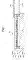
- FIG. 1 is a cross sectional view illustrating the first example of a touchscreen panel 60.
- FIG. 2 is a cross sectional view illustrating the touchscreen panel 60 accommodated within a casing 70.
- a direction perpendicular to an operation screen of the touchscreen panel is referred to as an up-and-down direction
- the side on the operation screen of the touchscreen panel is referred to as an upper side
- the side on a back surface of the touchscreen panel, opposite to the operation screen is referred to as a lower side.
- the above direction and sides are similarly referred to in FIG. 2 through FIG. 14 which will be described later.
- the touchscreen panel 60 includes a lower substrate 610, an upper sheet 630, a static-removing film 650, an FPC 660 for static removal, and an FPC 670 for position detection.
- the lower substrate 610 includes a glass substrate 611, and an ITO (Indium Tin Oxide) film 612 formed on an upper surface of the substrate 611.
- the upper sheet 630 includes a PET (Poly-Ethylene Terephthalate) film 631, and an ITO film 632 formed on a lower surface of the film 631.
- the static-removing film 650 includes a PET film 651, and a conductive film 652 formed on an upper surface of the film 651.
- One end of the FPC 660 is fixed to an outer peripheral on an upper surface of the static-removing film 650, and the FPC 660 extends outward in a horizontal direction from the outer peripheral of the static-removing film 650.
- a terminal on the one end of the FPC 660 is electrically connected to the conductive film 652, and a terminal on the other end of the FPC 660 is electrically connected to ground (that is, grounded).
- the FPC 670 is fixed to an outer peripheral on the upper surface of the substrate 611, and the FPC 670 extends outward in the horizontal direction from the outer peripheral of the substrate 611. Further, although illustration is omitted, the FPC 670 includes a plurality of independent wiring patterns, and terminals of the FPC 670 respectively are electrically connected to an electrode formed on the ITO film 612 and an electrode formed in the ITO film 633. The electrode formed on the ITO film 612 and the terminal formed on the FPC 670 are electrically connected via a wiring pattern formed on the substrate 611.
- the electrode formed on the ITO film 632 and the terminal formed on the FPC 670 are electrically connected via a wiring pattern formed on the film 631, the wiring pattern formed on the substrate 611, and a conductive material electrically connecting the wiring pattern on the film 631 and the wiring pattern on the substrate 611.
- a casing 70 that accommodates the touchscreen panel 60 is provided with an opening 71 so that the outer peripheral on the upper surface of the touchscreen panel 60 is concealed by the casing 70.
- the opening 71 has a rectangular shape in a plan view.
- the touchscreen panel 60 is viewed from the side of the operation screen, it is possible to conceal an adhesive layer 620, electrodes and wiring patterns provided on the upper sheet 630 and the lower substrate 610, the FPCs 660 and 670, or the like.
- the FPC 660 is arranged so that the FPC 660 is not visible through the opening 71, a stepped part or a difference in surface levels exists between the operation screen of the touchscreen panel 60 and a top surface 72 of the casing 70.
- FIG. 3 is a cross sectional view illustrating the second example of a touchscreen panel 80.
- FIG. 4 is a cross sectional view illustrating the touchscreen panel 80 accommodated within a casing 90.
- the touchscreen panel 80 includes a lower substrate 810, an upper sheet 830, a decoration film 850, and an FPC 860.
- the lower substrate 810 includes a glass substrate 811, and an ITO film 812 formed on an upper surface of the substrate 811.
- the upper sheet 830 includes a PET film 831, and an ITO film 832 formed on a lower surface of the film 831.
- One end of the FPC 860 is fixed to an outer peripheral on the upper surface of the substrate 811, and the FPC 860 extends outward in the horizontal direction from the outer peripheral of the substrate 811 through the elongated hole.
- the FPC 860 includes a plurality of wiring patterns, and terminals of the FPC 860 respectively are electrically connected to an electrode formed on the ITO film 812 and an electrode formed in the ITO film 832.
- the electrode formed on the ITO film 812 and the terminal formed on the FPC 860 are electrically connected via a wiring pattern formed on the substrate 811.
- the electrode formed on the ITO film 832 and the terminal formed on the FPC 860 are electrically connected via a wiring pattern formed on the film 831, the wiring pattern formed on the substrate 811, and a conductive material electrically connecting the wiring pattern on the film 831 and the wiring pattern on the substrate 811.
- the casing 90 that accommodates the touchscreen panel 80 is provided with an opening 91 having a rectangular shape in a plan view. As illustrated in FIG. 4 , the touchscreen panel 80 is arranged to fit into the opening 91. Hence, no stepped part or a difference in surface levels exists between the operation screen of the touchscreen panel 80 and a top surface 92 of the casing 90, to form a flush surface.
- the decoration film 850 includes a decoration part that is printed with a decoration, and a transparent part having no decoration.
- the decoration part is provided in a shape of a frame on an outer peripheral of the decoration film 850 so as to surround the transparent part.
- the decoration part conceals an adhesive layer 820, electrodes and wiring patterns provided on the upper sheet 830 and the lower substrate 810, the FPC 860, or the like.
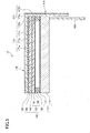
- FIG. 5 is a cross sectional view of the touchscreen panel 10.
- FIG. 6 is a cross sectional view of the touchscreen panel 10 accommodated within a casing 30.
- the touchscreen panel 10 includes a lower substrate 110, an upper sheet 130, a decoration film 150, a static-removing film 170, a lead 175 for static removal, and an FPC 190 for coordinate detection.
- the lower substrate 110 includes a glass substrate 111, and an ITO film 112 formed on an upper surface of the substrate 111.
- the upper sheet 130 includes a PET film 131, and an ITO film 132 formed on a lower surface of the film 131.
- the static-removing film 170 includes a PET film 171, and a conductive film 172 formed on an upper surface of the film 171.
- a stacked structure including the lower substrate 110 up to the decoration film 150 is referred to as a main body 100.
- the ITO film 112 which is a transparent conductive film, is formed on the upper surface of the substrate 111, which is a base material. Although illustration is omitted, electrodes and wiring patterns for wiring the FPC 190 are printed at an outer peripheral on the upper surface of the lower substrate 110.
- An adhesive layer 120 is formed in a frame shape on the upper surface of the lower substrate 110.
- the adhesive layer 120 fixes the upper sheet 130 on the lower substrate 110, and also functions as a spacer that separates the ITO film 132 and the ITO film 112 in a non-pressed state in which the touchscreen panel 10 is not pressed.
- the ITO film 132 which is a transparent conductive film, is formed on the power surface of the film 131, which is a flexible base. Although illustration is omitted, electrodes and wiring patterns for wiring the FPC 190 are printed at an outer peripheral on a lower surface of the upper sheet 130.
- an elongated hole that penetrates the substrate 111 from the upper surface to a lower surface thereof, is formed in the substrate 111 on the right side in FIG. 5 .
- One end of the FPC 190 is fixed to an outer peripheral on the upper surface of the substrate 111, and the FPC 190 extends outward in a vertical direction from the outer peripheral of the substrate 111 through the elongated hole.
- the FPC 190 includes a plurality of wiring patterns, and terminals of the FPC 190 respectively are electrically connected to an electrode formed on the ITO film 112 and an electrode formed in the ITO film 132.
- the electrode formed on the ITO film 112 and the terminal formed on the FPC 190 are electrically connected via a wiring pattern formed on the substrate 111.
- the electrode formed on the ITO film 132 and the terminal formed on the FPC 190 are electrically connected via a wiring pattern formed on the film 131, the wiring pattern formed on the substrate 111, and a conductive material electrically connecting the wiring pattern on the film 131 and the wiring pattern on the substrate 111.
- Terminals on the other end of the FPC 190 are electrically connected to a controller 20 illustrated in FIG. 6 .
- the touchscreen panel 10 is a resistive touchscreen panel.
- the upper sheet 130 flexes at the pressed position, and the ITO film 112 and the ITO film 132 make contact and conduct at the pressed position.
- the controller 20 applies a voltage across predetermined electrodes, and detects voltages at other electrodes, to detect the pressed position.
- the electrodes are arranged on the ITO film 112 separated along a first direction, and the electrodes are arranged on the ITO film 132 separated along a second direction intersecting the first direction.
- the controller 20 applies a voltage across the electrodes formed on the ITO film 112, and detects a voltage across the electrodes of the upper sheet 130, to detect a coordinate along the first direction.
- the controller 20 applies a voltage across the electrodes formed on the ITO film 132, and detects a voltage across the electrodes of the lower substrate 110, to detect a coordinate along the second direction.
- the touchscreen panel 10 is not limited to the 4-wire resistive touchscreen panel, and may be formed by other kinds or types of touchscreen panels.
- An adhesive layer 140 adheres the upper sheet 130 and the decoration film 150 to each other.
- the decoration film 150 is flexible, and is formed by a PET film, for example.
- the decoration film 150 includes a decoration part 151 that is printed with a decoration, and a transparent part 152 having no decoration.
- the decoration part 151 is provided in a shape of a frame on an outer peripheral of the decoration film 150 so as to surround the transparent part 152.
- the decoration part 151 conceals the adhesive layer 120, the electrodes and the wiring patterns provided on the upper sheet 130 and the lower substrate 110, the FPC 190, or the like.
- An adhesive layer 160 adheres the decoration film 150 and the static-removing film 170 to each other.
- the static-removing film 170 and the lead 175 are made of a transparent and flexible base, and may be formed by the PET film 171, for example.
- the PET film 171 includes a panel part 171a laminated on the decoration film 150, a lead 171b extending from the panel part 171a, and a flexible part 171c formed between the panel part 171a and the lead 171b.
- the conductive film 172 is formed on a surface of the PET film 171 closer to or facing the operation screen.
- the conductive film 172 is formed to span from the panel part 171a to the lead 171b via the flexible part 171c.
- a conductive film 172a formed on the panel part 171a and a conductive film 172b formed on the lead 171b are electrically connected via a conductive film 172c formed on the flexible part 171c.
- the conductive film 172b is grounded, as illustrated in FIG. 6 .
- the operator touches the conductive film 172a when the operator operates the touchscreen panel 10, and thus, electrostatic accumulated in the operator can be discharged to the ground through the conductive film 172b.
- the conductive film 172 may be made of any transparent and conductive material, and may be formed by an ITO film, for example.
- the conductive film 172 may be formed by coating and curing a paste, that is made of a resin and including a conductive material mixed and dispersed therein, on the PET film 171.
- the resin may be a UV-curing (Ultra-Violet-curing) epoxy acrylate resin, for example
- the conductive material may be a transparent conductive polymer, for example.
- the casing 30 that accommodates the touchscreen panel 10 is provided with an opening 31 having a rectangular shape in a plan view. As illustrated in FIG. 6 , in the casing 30 that accommodates the touchscreen panel 10, the touchscreen panel 10 is arranged to fit into the opening 31. Hence, no stepped part or a difference in surface levels exists between the operation screen of the touchscreen panel 10 and a top surface 32 of a frame of the casing 30, to form a flush surface.
- the frame of the casing 30 defines the opening 31.
- FIG. 7 is a development view illustrating the static-removing film 170 and the lead 175.
- the static-removing film 170 and the lead 175 are integrally formed, and the PET film 171 is bent by 90 degrees at a boundary between the panel part 171a and the lead 171b, that is, by bending the lead 171b in a perpendicular direction with respect to the panel part 171a.
- a thickness of the static-removing film 170 and a thickness of the lead 175 are approximately the same.
- the static-removing film 170 and the lead 175 may be formed by forming the conductive film 172 on the PET film 171 that is cut into a predetermined shape, and bending the lead 175 by 90 degrees so that the surface formed with the conductive film 172 faces the outer side.
- FIG. 8 is a plan view of the main body 100 viewed from the operation screen.
- FIG. 9 is a perspective view of the main body 100.
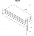
- FIG. 10 is a perspective view illustrating the touchscreen panel 10.
- a cutout 180 that is a groove extending in the downward direction, is formed in the main body 100.
- the lead 175 that extends in the downward direction from the static-removing film 170 is arranged in the cutout 180.
- the lead 175 can be arranged so as not to protrude outside from the side surface of the main body 100, and the touchscreen panel 10 can be arranged to fit within the opening 31.
- no stepped part or a difference in surface levels exists between the operation screen of the touchscreen panel 10 and the top surface 32 of the frame of the casing 30, to form a flush surface.
- the touchscreen panel 10 in this embodiment it is possible to provide a function to remove electrostatics, and simultaneously form the flush surface such that no stepped part or the difference in surface levels exist between the operation screen of the touchscreen panel 10 and the top surface 32 of the frame of the casing 30.
- touchscreen panel 10 is described above by way of one embodiment, the present invention is not limited to the embodiment, and various variations, modifications, and substitutions may be made without departing from the scope of the present invention.
- the touchscreen panel 10 uses, as the base material forming the ITO film, the substrate 111, and the PET film 131.
- both the substrate 111 and the PET film 131 may use the PET film, for example.
- the main body 100 described above is provided with the decoration film 150, the decoration film 150 may be omitted.
- the main body 100 may be formed by a stacked structure including the lower substrate 110 up to the upper sheet 130.
- a decoration part can be printed on the upper surface of the PET film 131, so that the upper sheet 130 may function as a decoration film, without using the decoration film 150.
- a decoration part can be printed on the lower surface of the static-removing film 170, so that the static-removing film 170 may function as a decoration film, without using the decoration film 150. In such cases, the decoration can be provided, while simultaneously reducing the number of films that are stacked.
- the cutout 180 is provided in the main body 100.
- the touchscreen panel 10 is not limited the structure including the cutout 180 in the main body 100.
- FIG. 11 is a cross sectional view illustrating a touchscreen panel 10A in a first modification.
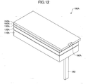
- FIG. 12 is a perspective view of a main body 100A of the touchscreen panel 10A.
- a cutout 180A may be provided only in the decoration film 150A.
- a lead 175A can also extend in the downward direction in the cutout 180A of the main body 100A.
- FIG. 13 is a cross sectional view illustrating a touchscreen panel 10B in a second modification.
- FIG. 14 is a perspective view of a main body 100B of the touchscreen panel 10B.
- a cutout 180B may be provided in both the substrate 111 and the PET film 131.
- a lead 175B can also extend in the downward direction in the cutout 180B of the main body 100B.
- a touchscreen panel having a function to remove electrostatics, and a flush surface such that no stepped part or a difference in surface levels exist between a casing and an operation screen.
- the casing, and the touchscreen panel accommodated within the casing may form a display apparatus.
Landscapes
- Engineering & Computer Science (AREA)
- General Engineering & Computer Science (AREA)
- Theoretical Computer Science (AREA)
- Human Computer Interaction (AREA)
- Physics & Mathematics (AREA)
- General Physics & Mathematics (AREA)
- Position Input By Displaying (AREA)
Abstract
Description
- The embodiments discussed herein are related to a touchscreen panel.
- Touchscreen panels that can prevent an erroneous operation by removing electrostatics are proposed in Japanese Laid-Open Patent Publication No.
2012-181781 2015-125471 6246584 - On the other hand, touchscreen panels having a flush-surface design are proposed, as touchscreen panels having appealing design. According to the flush-surface design, a frame of a casing and an operation screen of the touchscreen panel form a flush surface and no stepped part or a difference in surface levels exist between the frame and the operation screen.
- However, according to a structure proposed in Japanese Laid-Open Patent Publication No.
2012-181781 2015-125471 6246584 - Accordingly, it is an object in one aspect of the embodiments to provide a touchscreen panel having a function to remove electrostatics, and a flush surface such that no stepped part or a difference in surface levels exist between a casing and an operation screen of the touchscreen panel.
- According to one aspect of embodiments of the present invention, a touchscreen panel includes a main body including a lower substrate that includes a first transparent conductive film, and an upper sheet that includes a second transparent conductive film; a static-removing film, arranged on the main body, and including a conductive film; and a lead including a conductive part electrically connected to the conductive film, wherein the main body includes a cutout in which the lead is arranged.
- Other objects and further features of the present invention will be apparent from the following detailed description when read in conjunction with the accompanying drawings.
-
-
FIG. 1 is a cross sectional view illustrating a first example of a touchscreen panel; -
FIG. 2 is a cross sectional view illustrating the first example of the touchscreen panel accommodated within a casing; -
FIG. 3 is a cross sectional view illustrating a second example of the touchscreen panel; -
FIG. 4 is a cross sectional view illustrating the second example of the touchscreen panel accommodated within the casing; -
FIG. 5 is a cross sectional view illustrating a touchscreen panel in one embodiment; -
FIG. 6 is a cross sectional view illustrating the touchscreen panel in one embodiment accommodated within a casing; -
FIG. 7 is a development view illustrating a static-removing film and a lead; -
FIG. 8 is a plan view of a main body viewed from an operation screen; -
FIG. 9 is a perspective view of the main body; -
FIG. 10 is a perspective view illustrating the touchscreen panel in one embodiment; -
FIG. 11 is a cross sectional view illustrating the touchscreen panel in a first modification; -
FIG. 12 is a perspective view of the main body in the first modification; -
FIG. 13 is a cross sectional view illustrating the touchscreen panel in a second modification; and -
FIG. 14 is a perspective view of the touchscreen panel in the second modification. - Embodiments of a touchscreen panel according to the present invention will be described, by referring to the drawings.
- A first example of the structure of the touchscreen panel will be described, by referring to
FIG. 1 andFIG. 2 .FIG. 1 is a cross sectional view illustrating the first example of atouchscreen panel 60.FIG. 2 is a cross sectional view illustrating thetouchscreen panel 60 accommodated within acasing 70. In the following description, a direction perpendicular to an operation screen of the touchscreen panel is referred to as an up-and-down direction, the side on the operation screen of the touchscreen panel is referred to as an upper side, and the side on a back surface of the touchscreen panel, opposite to the operation screen, is referred to as a lower side. The above direction and sides are similarly referred to inFIG. 2 through FIG. 14 which will be described later. - As illustrated in
FIG. 1 , thetouchscreen panel 60 includes alower substrate 610, anupper sheet 630, a static-removingfilm 650, an FPC 660 for static removal, and an FPC 670 for position detection. Thelower substrate 610 includes aglass substrate 611, and an ITO (Indium Tin Oxide)film 612 formed on an upper surface of thesubstrate 611. Theupper sheet 630 includes a PET (Poly-Ethylene Terephthalate)film 631, and an ITOfilm 632 formed on a lower surface of thefilm 631. The static-removingfilm 650 includes aPET film 651, and aconductive film 652 formed on an upper surface of thefilm 651. - One end of the FPC 660 is fixed to an outer peripheral on an upper surface of the static-removing
film 650, and the FPC 660 extends outward in a horizontal direction from the outer peripheral of the static-removingfilm 650. In addition, a terminal on the one end of the FPC 660 is electrically connected to theconductive film 652, and a terminal on the other end of the FPC 660 is electrically connected to ground (that is, grounded). - One end of the FPC 670 is fixed to an outer peripheral on the upper surface of the
substrate 611, and the FPC 670 extends outward in the horizontal direction from the outer peripheral of thesubstrate 611. Further, although illustration is omitted, the FPC 670 includes a plurality of independent wiring patterns, and terminals of the FPC 670 respectively are electrically connected to an electrode formed on theITO film 612 and an electrode formed in the ITO film 633. The electrode formed on the ITOfilm 612 and the terminal formed on the FPC 670 are electrically connected via a wiring pattern formed on thesubstrate 611. The electrode formed on the ITOfilm 632 and the terminal formed on the FPC 670 are electrically connected via a wiring pattern formed on thefilm 631, the wiring pattern formed on thesubstrate 611, and a conductive material electrically connecting the wiring pattern on thefilm 631 and the wiring pattern on thesubstrate 611. - As illustrated in
FIG. 2 , acasing 70 that accommodates thetouchscreen panel 60, is provided with anopening 71 so that the outer peripheral on the upper surface of thetouchscreen panel 60 is concealed by thecasing 70. The opening 71 has a rectangular shape in a plan view. Hence, when thetouchscreen panel 60 is viewed from the side of the operation screen, it is possible to conceal anadhesive layer 620, electrodes and wiring patterns provided on theupper sheet 630 and thelower substrate 610, theFPCs FIG. 2 , because the FPC 660 is arranged so that the FPC 660 is not visible through theopening 71, a stepped part or a difference in surface levels exists between the operation screen of thetouchscreen panel 60 and atop surface 72 of thecasing 70. - Next, a second example of the touchscreen panel will be described, by referring to
FIG. 3 andFIG. 4 .FIG. 3 is a cross sectional view illustrating the second example of atouchscreen panel 80.FIG. 4 is a cross sectional view illustrating thetouchscreen panel 80 accommodated within acasing 90. - As illustrated in
FIG. 3 , thetouchscreen panel 80 includes alower substrate 810, anupper sheet 830, adecoration film 850, and an FPC 860. Thelower substrate 810 includes aglass substrate 811, and an ITOfilm 812 formed on an upper surface of thesubstrate 811. Theupper sheet 830 includes aPET film 831, and an ITOfilm 832 formed on a lower surface of thefilm 831. - An elongated hole that penetrates the
substrate 811 from the upper surface to a lower surface thereof, is formed in thesubstrate 811 on the right side inFIG. 3 . One end of the FPC 860 is fixed to an outer peripheral on the upper surface of thesubstrate 811, and the FPC 860 extends outward in the horizontal direction from the outer peripheral of thesubstrate 811 through the elongated hole. Further, although illustration is omitted, the FPC 860 includes a plurality of wiring patterns, and terminals of the FPC 860 respectively are electrically connected to an electrode formed on theITO film 812 and an electrode formed in the ITOfilm 832. The electrode formed on the ITOfilm 812 and the terminal formed on the FPC 860 are electrically connected via a wiring pattern formed on thesubstrate 811. The electrode formed on the ITOfilm 832 and the terminal formed on the FPC 860 are electrically connected via a wiring pattern formed on thefilm 831, the wiring pattern formed on thesubstrate 811, and a conductive material electrically connecting the wiring pattern on thefilm 831 and the wiring pattern on thesubstrate 811. - The
casing 90 that accommodates thetouchscreen panel 80 is provided with an opening 91 having a rectangular shape in a plan view. As illustrated inFIG. 4 , thetouchscreen panel 80 is arranged to fit into theopening 91. Hence, no stepped part or a difference in surface levels exists between the operation screen of thetouchscreen panel 80 and atop surface 92 of thecasing 90, to form a flush surface. - The
decoration film 850 includes a decoration part that is printed with a decoration, and a transparent part having no decoration. The decoration part is provided in a shape of a frame on an outer peripheral of thedecoration film 850 so as to surround the transparent part. The decoration part conceals anadhesive layer 820, electrodes and wiring patterns provided on theupper sheet 830 and thelower substrate 810, theFPC 860, or the like. - A
touchscreen panel 10 in one embodiment will be described, by referring toFIG. 5 andFIG. 6 .FIG. 5 is a cross sectional view of thetouchscreen panel 10.FIG. 6 is a cross sectional view of thetouchscreen panel 10 accommodated within acasing 30. - As illustrated in
FIG. 5 , thetouchscreen panel 10 includes alower substrate 110, anupper sheet 130, adecoration film 150, a static-removingfilm 170, alead 175 for static removal, and anFPC 190 for coordinate detection. Thelower substrate 110 includes aglass substrate 111, and anITO film 112 formed on an upper surface of thesubstrate 111. Theupper sheet 130 includes aPET film 131, and anITO film 132 formed on a lower surface of thefilm 131. The static-removingfilm 170 includes aPET film 171, and aconductive film 172 formed on an upper surface of thefilm 171. In this embodiment, a stacked structure including thelower substrate 110 up to thedecoration film 150 is referred to as amain body 100. - In the
lower substrate 110, theITO film 112, which is a transparent conductive film, is formed on the upper surface of thesubstrate 111, which is a base material. Although illustration is omitted, electrodes and wiring patterns for wiring theFPC 190 are printed at an outer peripheral on the upper surface of thelower substrate 110. - An
adhesive layer 120 is formed in a frame shape on the upper surface of thelower substrate 110. Theadhesive layer 120 fixes theupper sheet 130 on thelower substrate 110, and also functions as a spacer that separates theITO film 132 and theITO film 112 in a non-pressed state in which thetouchscreen panel 10 is not pressed. - In the
upper sheet 130, theITO film 132, which is a transparent conductive film, is formed on the power surface of thefilm 131, which is a flexible base. Although illustration is omitted, electrodes and wiring patterns for wiring theFPC 190 are printed at an outer peripheral on a lower surface of theupper sheet 130. - Although illustration is omitted, an elongated hole, that penetrates the
substrate 111 from the upper surface to a lower surface thereof, is formed in thesubstrate 111 on the right side inFIG. 5 . One end of theFPC 190 is fixed to an outer peripheral on the upper surface of thesubstrate 111, and theFPC 190 extends outward in a vertical direction from the outer peripheral of thesubstrate 111 through the elongated hole. Further, although illustration is omitted, theFPC 190 includes a plurality of wiring patterns, and terminals of theFPC 190 respectively are electrically connected to an electrode formed on theITO film 112 and an electrode formed in theITO film 132. The electrode formed on theITO film 112 and the terminal formed on theFPC 190 are electrically connected via a wiring pattern formed on thesubstrate 111. The electrode formed on theITO film 132 and the terminal formed on theFPC 190 are electrically connected via a wiring pattern formed on thefilm 131, the wiring pattern formed on thesubstrate 111, and a conductive material electrically connecting the wiring pattern on thefilm 131 and the wiring pattern on thesubstrate 111. Terminals on the other end of theFPC 190 are electrically connected to acontroller 20 illustrated inFIG. 6 . - The
touchscreen panel 10 is a resistive touchscreen panel. When an operator presses thetouchscreen panel 10, theupper sheet 130 flexes at the pressed position, and theITO film 112 and theITO film 132 make contact and conduct at the pressed position. Thecontroller 20 applies a voltage across predetermined electrodes, and detects voltages at other electrodes, to detect the pressed position. For example, in the case of a 4-wire resistive touchscreen panel, the electrodes are arranged on theITO film 112 separated along a first direction, and the electrodes are arranged on theITO film 132 separated along a second direction intersecting the first direction. Thecontroller 20 applies a voltage across the electrodes formed on theITO film 112, and detects a voltage across the electrodes of theupper sheet 130, to detect a coordinate along the first direction. In addition, thecontroller 20 applies a voltage across the electrodes formed on theITO film 132, and detects a voltage across the electrodes of thelower substrate 110, to detect a coordinate along the second direction. Of course, thetouchscreen panel 10 is not limited to the 4-wire resistive touchscreen panel, and may be formed by other kinds or types of touchscreen panels. - An
adhesive layer 140 adheres theupper sheet 130 and thedecoration film 150 to each other. - The
decoration film 150 is flexible, and is formed by a PET film, for example. In addition, thedecoration film 150 includes adecoration part 151 that is printed with a decoration, and atransparent part 152 having no decoration. Thedecoration part 151 is provided in a shape of a frame on an outer peripheral of thedecoration film 150 so as to surround thetransparent part 152. When thetouchscreen panel 10 is viewed from above the operation screen, thedecoration part 151 conceals theadhesive layer 120, the electrodes and the wiring patterns provided on theupper sheet 130 and thelower substrate 110, theFPC 190, or the like. - An
adhesive layer 160 adheres thedecoration film 150 and the static-removingfilm 170 to each other. - The static-removing
film 170 and thelead 175 are made of a transparent and flexible base, and may be formed by thePET film 171, for example. ThePET film 171 includes apanel part 171a laminated on thedecoration film 150, a lead 171b extending from thepanel part 171a, and aflexible part 171c formed between thepanel part 171a and the lead 171b. - The
conductive film 172 is formed on a surface of thePET film 171 closer to or facing the operation screen. Theconductive film 172 is formed to span from thepanel part 171a to the lead 171b via theflexible part 171c. Aconductive film 172a formed on thepanel part 171a and aconductive film 172b formed on the lead 171b are electrically connected via aconductive film 172c formed on theflexible part 171c. - The
conductive film 172b is grounded, as illustrated inFIG. 6 . Hence, the operator touches theconductive film 172a when the operator operates thetouchscreen panel 10, and thus, electrostatic accumulated in the operator can be discharged to the ground through theconductive film 172b. - The
conductive film 172 may be made of any transparent and conductive material, and may be formed by an ITO film, for example. In addition, theconductive film 172 may be formed by coating and curing a paste, that is made of a resin and including a conductive material mixed and dispersed therein, on thePET film 171. In this case, the resin may be a UV-curing (Ultra-Violet-curing) epoxy acrylate resin, for example, and the conductive material may be a transparent conductive polymer, for example. - The
casing 30 that accommodates thetouchscreen panel 10 is provided with anopening 31 having a rectangular shape in a plan view. As illustrated inFIG. 6 , in thecasing 30 that accommodates thetouchscreen panel 10, thetouchscreen panel 10 is arranged to fit into theopening 31. Hence, no stepped part or a difference in surface levels exists between the operation screen of thetouchscreen panel 10 and atop surface 32 of a frame of thecasing 30, to form a flush surface. The frame of thecasing 30 defines theopening 31. - Next, the static-removing
film 170 and thelead 175 will further be described, by referring toFIG. 7. FIG. 7 is a development view illustrating the static-removingfilm 170 and thelead 175. - As illustrated in
FIG. 7 , the static-removingfilm 170 and thelead 175 are integrally formed, and thePET film 171 is bent by 90 degrees at a boundary between thepanel part 171a and the lead 171b, that is, by bending the lead 171b in a perpendicular direction with respect to thepanel part 171a. Hence, as illustrated inFIG. 5 , a thickness of the static-removingfilm 170 and a thickness of thelead 175 are approximately the same. - The static-removing
film 170 and thelead 175 may be formed by forming theconductive film 172 on thePET film 171 that is cut into a predetermined shape, and bending thelead 175 by 90 degrees so that the surface formed with theconductive film 172 faces the outer side. -
FIG. 8 is a plan view of themain body 100 viewed from the operation screen.FIG. 9 is a perspective view of themain body 100.FIG. 10 is a perspective view illustrating thetouchscreen panel 10. - As illustrated in
FIG. 8 andFIG. 9 , acutout 180, that is a groove extending in the downward direction, is formed in themain body 100. In addition, as illustrated inFIG. 10 , thelead 175 that extends in the downward direction from the static-removingfilm 170 is arranged in thecutout 180. For this reason, thelead 175 can be arranged so as not to protrude outside from the side surface of themain body 100, and thetouchscreen panel 10 can be arranged to fit within theopening 31. Hence, no stepped part or a difference in surface levels exists between the operation screen of thetouchscreen panel 10 and thetop surface 32 of the frame of thecasing 30, to form a flush surface. - According to the
touchscreen panel 10 in this embodiment, it is possible to provide a function to remove electrostatics, and simultaneously form the flush surface such that no stepped part or the difference in surface levels exist between the operation screen of thetouchscreen panel 10 and thetop surface 32 of the frame of thecasing 30. - Although the
touchscreen panel 10 is described above by way of one embodiment, the present invention is not limited to the embodiment, and various variations, modifications, and substitutions may be made without departing from the scope of the present invention. - In the embodiment described above, the
touchscreen panel 10 uses, as the base material forming the ITO film, thesubstrate 111, and thePET film 131. However, both thesubstrate 111 and thePET film 131 may use the PET film, for example. - In addition, the
main body 100 described above is provided with thedecoration film 150, thedecoration film 150 may be omitted. In a case in which nodecoration film 150 is provided, themain body 100 may be formed by a stacked structure including thelower substrate 110 up to theupper sheet 130. - Further, a decoration part can be printed on the upper surface of the
PET film 131, so that theupper sheet 130 may function as a decoration film, without using thedecoration film 150. Similarly, a decoration part can be printed on the lower surface of the static-removingfilm 170, so that the static-removingfilm 170 may function as a decoration film, without using thedecoration film 150. In such cases, the decoration can be provided, while simultaneously reducing the number of films that are stacked. - In the
touchscreen panel 10 described above, thecutout 180 is provided in themain body 100. However, thetouchscreen panel 10 is not limited the structure including thecutout 180 in themain body 100. -
FIG. 11 is a cross sectional view illustrating atouchscreen panel 10A in a first modification.FIG. 12 is a perspective view of amain body 100A of thetouchscreen panel 10A. - In a case in which a
decoration film 150A is larger than aglass substrate 111A and aPET film 131A, acutout 180A may be provided only in thedecoration film 150A. According to this modification, alead 175A can also extend in the downward direction in thecutout 180A of themain body 100A. Hence, similarly as in the case of thetouchscreen panel 10 described above, it is possible to provide a function to remove electrostatics, and simultaneously form the flush surface such that no stepped part or the difference in surface levels exist between the operation screen and the top surface of the casing. -
FIG. 13 is a cross sectional view illustrating atouchscreen panel 10B in a second modification.FIG. 14 is a perspective view of amain body 100B of thetouchscreen panel 10B. - In a case in which a
decoration film 150B is smaller than thesubstrate 111 and thePET film 131, acutout 180B may be provided in both thesubstrate 111 and thePET film 131. According to this modification, a lead 175B can also extend in the downward direction in thecutout 180B of themain body 100B. Hence, similarly as in the case of thetouchscreen panel 10 described above, it is possible to provide a function to remove electrostatics, and simultaneously form the flush surface such that no stepped part or the difference in surface levels exist between the operation screen of thetouchscreen panel 10B and the top surface of the frame of the casing. - According to the embodiments and modifications described above, it is possible to provide a touchscreen panel having a function to remove electrostatics, and a flush surface such that no stepped part or a difference in surface levels exist between a casing and an operation screen.
- The casing, and the touchscreen panel accommodated within the casing, may form a display apparatus.
- Although the modifications are numbered with, for example, "first," and "second," the ordinal numbers do not imply priorities of the modifications.
- Further, the present invention is not limited to these embodiments, but various variations and modifications may be made without departing from the scope of the present invention.
Claims (6)
- A touchscreen panel (10, 10A, 10B) comprising:a main body (100, 100A, 100B) including a lower substrate (110) that includes a first transparent conductive film (112), and an upper sheet (130) that includes a second transparent conductive film (132);a static-removing film (170), arranged on the main body, and including a conductive film (172); anda lead (175, 175A, 175B) including a conductive part (172b, 172c) electrically connected to the conductive film,wherein the main body includes a cutout (180, 180A, 180B) in which the lead is arranged.
- The touchscreen panel (10, 10A, 10B) as claimed in claim 1, further comprising:a flexible part (171c), provided between the static-removing film (170) and the lead (175, 175A, 175B), bending the lead in a vertical direction to the static-removing film.
- The touchscreen panel (10, 10A, 10B)as claimed in claim 1 or 2, wherein the lead (175, 175A, 175B) extends outward from the static-removing film (170) in a direction towards the lower substrate (110).
- The touchscreen panel (10, 10A, 10B) as claimed in any of claims 1 to 3, further comprising:a decoration film (150) provided on the second transparent conductive film (132),wherein the cutout (175, 175A, 175B) is formed in at least the decoration film.
- The touchscreen panel (10, 10B) as claimed in claim 4, wherein the cutout (175, 175B) is formed in the lower substrate (110) and the upper sheet (130).
- A display apparatus comprising:a touchscreen panel (10, 10A, 10B) according to any one of claims 1 to 5, and including an operation screen; anda casing (30), having a frame that defines an opening (31) thereof, and configured to accommodate the touchscreen panel arranged to fit into the opening,wherein the operation screen of the touchscreen panel and a top surface (32) of the frame form a flush surface.
Applications Claiming Priority (1)
| Application Number | Priority Date | Filing Date | Title |
|---|---|---|---|
| JP2018025670A JP2019144625A (en) | 2018-02-16 | 2018-02-16 | Touch panel |
Publications (2)
| Publication Number | Publication Date |
|---|---|
| EP3528100A1 true EP3528100A1 (en) | 2019-08-21 |
| EP3528100B1 EP3528100B1 (en) | 2021-04-07 |
Family
ID=65199302
Family Applications (1)
| Application Number | Title | Priority Date | Filing Date |
|---|---|---|---|
| EP19152456.0A Active EP3528100B1 (en) | 2018-02-16 | 2019-01-18 | Touchscreen panel |
Country Status (4)
| Country | Link |
|---|---|
| US (1) | US10838531B2 (en) |
| EP (1) | EP3528100B1 (en) |
| JP (1) | JP2019144625A (en) |
| CN (1) | CN110162231A (en) |
Citations (7)
| Publication number | Priority date | Publication date | Assignee | Title |
|---|---|---|---|---|
| JPS6246584B2 (en) | 1978-08-17 | 1987-10-02 | Schenectady Chemical | |
| EP2244172A2 (en) * | 2009-04-21 | 2010-10-27 | Fujitsu Component Limited | Touchscreen panel, electronic apparatus and method of fabricating touchscreen panel |
| US20110205183A1 (en) * | 2008-11-19 | 2011-08-25 | Sharp Kabushiki Kaisha | Touch panel and display device including the same |
| JP2012181781A (en) | 2011-03-02 | 2012-09-20 | Fujitsu Component Ltd | Touch panel and mounting method |
| EP2584437A2 (en) * | 2010-06-16 | 2013-04-24 | Samwon St | Touch panel sensor |
| US20150160760A1 (en) * | 2012-09-13 | 2015-06-11 | Wonder Future Corporation | Touch panel, method for manufacturing touch panel, and touch panel integrated display device |
| JP2015125471A (en) | 2013-12-25 | 2015-07-06 | 富士通コンポーネント株式会社 | Touch panel device |
Family Cites Families (17)
| Publication number | Priority date | Publication date | Assignee | Title |
|---|---|---|---|---|
| CA2551595C (en) * | 2003-12-26 | 2011-02-08 | Nissha Printing Co., Ltd. | Electronic device with protection panel, protection panel, and method offabricating protection panels |
| JP2009086077A (en) * | 2007-09-28 | 2009-04-23 | Hitachi Displays Ltd | Liquid crystal display device equipped with touch panel and manufacturing method thereof |
| JP4944975B2 (en) * | 2010-04-14 | 2012-06-06 | パナソニック株式会社 | Touch panel device |
| US8692948B2 (en) * | 2010-05-21 | 2014-04-08 | Apple Inc. | Electric field shielding for in-cell touch type thin-film-transistor liquid crystal displays |
| JP5740114B2 (en) * | 2010-08-19 | 2015-06-24 | 株式会社ジャパンディスプレイ | Display device |
| JP2012141801A (en) * | 2010-12-28 | 2012-07-26 | Fujitsu Component Ltd | Touch panel |
| KR20120097146A (en) * | 2011-02-24 | 2012-09-03 | 엘지디스플레이 주식회사 | Liquid crystal display device |
| US8952911B2 (en) * | 2012-08-08 | 2015-02-10 | Creator Technology B.V. | Electronic device with a touch sensitive panel, method for operating the electronic device, and display system |
| JP5768031B2 (en) * | 2012-10-22 | 2015-08-26 | アルプス電気株式会社 | Surface panel having detection function and manufacturing method thereof |
| CN103324341A (en) * | 2013-06-07 | 2013-09-25 | 业成光电(深圳)有限公司 | Touch panel and electronic device with touch panel |
| US10180700B2 (en) * | 2013-07-01 | 2019-01-15 | Lg Display Co., Ltd. | Display device |
| KR102178797B1 (en) * | 2013-10-04 | 2020-11-16 | 삼성디스플레이 주식회사 | Display device comprising touch sensors |
| KR102238920B1 (en) * | 2014-12-03 | 2021-04-13 | 엘지디스플레이 주식회사 | Lquid crystal display device |
| US10042224B2 (en) * | 2015-06-05 | 2018-08-07 | Innolux Corporation | Touch display panel and touch display device using the same |
| US10152146B2 (en) * | 2015-09-16 | 2018-12-11 | Microsoft Technology Licensing, Llc | Cosmetically hidden electrostatic discharge protection structures |
| JP2017068819A (en) * | 2015-09-28 | 2017-04-06 | 双葉電子工業株式会社 | Touch panel |
| TWI761679B (en) * | 2017-03-28 | 2022-04-21 | 日商日東電工股份有限公司 | Polarizing film with adhesive layer, and polarizing film with adhesive layer for built-in liquid crystal panel |
-
2018
- 2018-02-16 JP JP2018025670A patent/JP2019144625A/en active Pending
-
2019
- 2019-01-18 EP EP19152456.0A patent/EP3528100B1/en active Active
- 2019-01-18 US US16/251,610 patent/US10838531B2/en not_active Expired - Fee Related
- 2019-01-31 CN CN201910094313.0A patent/CN110162231A/en active Pending
Patent Citations (7)
| Publication number | Priority date | Publication date | Assignee | Title |
|---|---|---|---|---|
| JPS6246584B2 (en) | 1978-08-17 | 1987-10-02 | Schenectady Chemical | |
| US20110205183A1 (en) * | 2008-11-19 | 2011-08-25 | Sharp Kabushiki Kaisha | Touch panel and display device including the same |
| EP2244172A2 (en) * | 2009-04-21 | 2010-10-27 | Fujitsu Component Limited | Touchscreen panel, electronic apparatus and method of fabricating touchscreen panel |
| EP2584437A2 (en) * | 2010-06-16 | 2013-04-24 | Samwon St | Touch panel sensor |
| JP2012181781A (en) | 2011-03-02 | 2012-09-20 | Fujitsu Component Ltd | Touch panel and mounting method |
| US20150160760A1 (en) * | 2012-09-13 | 2015-06-11 | Wonder Future Corporation | Touch panel, method for manufacturing touch panel, and touch panel integrated display device |
| JP2015125471A (en) | 2013-12-25 | 2015-07-06 | 富士通コンポーネント株式会社 | Touch panel device |
Also Published As
| Publication number | Publication date |
|---|---|
| JP2019144625A (en) | 2019-08-29 |
| CN110162231A (en) | 2019-08-23 |
| US20190258347A1 (en) | 2019-08-22 |
| EP3528100B1 (en) | 2021-04-07 |
| US10838531B2 (en) | 2020-11-17 |
Similar Documents
| Publication | Publication Date | Title |
|---|---|---|
| CN1207654C (en) | Touch panel and electronic equipment using the touch panel | |
| US7439466B2 (en) | Touch panel | |
| US9117413B2 (en) | Touch panel and touch display device | |
| US7494358B2 (en) | Touch panel | |
| US20030174128A1 (en) | Coordinate input device and liquid crystal display device with such device | |
| US8049127B2 (en) | Touch panel | |
| CN100583018C (en) | Touch panel and manufacturing method thereof | |
| KR20110109336A (en) | Touch screen panel device | |
| US10061414B2 (en) | Touch panel | |
| EP1783588A1 (en) | Touch panel | |
| EP2511805A2 (en) | Touch panel and mobile terminal having the touch panel | |
| EP2541381B1 (en) | Input device, display device, and portable terminal | |
| KR100997712B1 (en) | Slim Windows Touchscreen Panel | |
| US9983701B2 (en) | Touch panel | |
| CN101615095B (en) | Integrated touch panel and electronic device using it | |
| US20150220185A1 (en) | Touch panel | |
| US9124275B2 (en) | Touch panel | |
| EP3528100B1 (en) | Touchscreen panel | |
| KR20160005596A (en) | Touch window | |
| KR101568779B1 (en) | Capacitive force sensing system using conventional capacitive touch layers | |
| WO2011159079A2 (en) | Capacitive touch panel integrated with window panel | |
| US20250147617A1 (en) | Touch sensor | |
| KR20150087548A (en) | Touch panel | |
| KR100647574B1 (en) | Touch panel | |
| KR20160013696A (en) | Touch panel |
Legal Events
| Date | Code | Title | Description |
|---|---|---|---|
| PUAI | Public reference made under article 153(3) epc to a published international application that has entered the european phase |
Free format text: ORIGINAL CODE: 0009012 |
|
| STAA | Information on the status of an ep patent application or granted ep patent |
Free format text: STATUS: THE APPLICATION HAS BEEN PUBLISHED |
|
| AK | Designated contracting states |
Kind code of ref document: A1 Designated state(s): AL AT BE BG CH CY CZ DE DK EE ES FI FR GB GR HR HU IE IS IT LI LT LU LV MC MK MT NL NO PL PT RO RS SE SI SK SM TR |
|
| AX | Request for extension of the european patent |
Extension state: BA ME |
|
| STAA | Information on the status of an ep patent application or granted ep patent |
Free format text: STATUS: REQUEST FOR EXAMINATION WAS MADE |
|
| 17P | Request for examination filed |
Effective date: 20200212 |
|
| RBV | Designated contracting states (corrected) |
Designated state(s): AL AT BE BG CH CY CZ DE DK EE ES FI FR GB GR HR HU IE IS IT LI LT LU LV MC MK MT NL NO PL PT RO RS SE SI SK SM TR |
|
| GRAP | Despatch of communication of intention to grant a patent |
Free format text: ORIGINAL CODE: EPIDOSNIGR1 |
|
| STAA | Information on the status of an ep patent application or granted ep patent |
Free format text: STATUS: GRANT OF PATENT IS INTENDED |
|
| INTG | Intention to grant announced |
Effective date: 20200616 |
|
| GRAJ | Information related to disapproval of communication of intention to grant by the applicant or resumption of examination proceedings by the epo deleted |
Free format text: ORIGINAL CODE: EPIDOSDIGR1 |
|
| STAA | Information on the status of an ep patent application or granted ep patent |
Free format text: STATUS: REQUEST FOR EXAMINATION WAS MADE |
|
| INTC | Intention to grant announced (deleted) | ||
| GRAS | Grant fee paid |
Free format text: ORIGINAL CODE: EPIDOSNIGR3 |
|
| STAA | Information on the status of an ep patent application or granted ep patent |
Free format text: STATUS: GRANT OF PATENT IS INTENDED |
|
| GRAP | Despatch of communication of intention to grant a patent |
Free format text: ORIGINAL CODE: EPIDOSNIGR1 |
|
| INTG | Intention to grant announced |
Effective date: 20201209 |
|
| GRAA | (expected) grant |
Free format text: ORIGINAL CODE: 0009210 |
|
| STAA | Information on the status of an ep patent application or granted ep patent |
Free format text: STATUS: THE PATENT HAS BEEN GRANTED |
|
| AK | Designated contracting states |
Kind code of ref document: B1 Designated state(s): AL AT BE BG CH CY CZ DE DK EE ES FI FR GB GR HR HU IE IS IT LI LT LU LV MC MK MT NL NO PL PT RO RS SE SI SK SM TR |
|
| REG | Reference to a national code |
Ref country code: GB Ref legal event code: FG4D |
|
| REG | Reference to a national code |
Ref country code: AT Ref legal event code: REF Ref document number: 1380554 Country of ref document: AT Kind code of ref document: T Effective date: 20210415 Ref country code: CH Ref legal event code: EP |
|
| REG | Reference to a national code |
Ref country code: DE Ref legal event code: R096 Ref document number: 602019003627 Country of ref document: DE |
|
| REG | Reference to a national code |
Ref country code: IE Ref legal event code: FG4D |
|
| REG | Reference to a national code |
Ref country code: LT Ref legal event code: MG9D |
|
| REG | Reference to a national code |
Ref country code: NL Ref legal event code: MP Effective date: 20210407 Ref country code: AT Ref legal event code: MK05 Ref document number: 1380554 Country of ref document: AT Kind code of ref document: T Effective date: 20210407 |
|
| PG25 | Lapsed in a contracting state [announced via postgrant information from national office to epo] |
Ref country code: HR Free format text: LAPSE BECAUSE OF FAILURE TO SUBMIT A TRANSLATION OF THE DESCRIPTION OR TO PAY THE FEE WITHIN THE PRESCRIBED TIME-LIMIT Effective date: 20210407 Ref country code: LT Free format text: LAPSE BECAUSE OF FAILURE TO SUBMIT A TRANSLATION OF THE DESCRIPTION OR TO PAY THE FEE WITHIN THE PRESCRIBED TIME-LIMIT Effective date: 20210407 Ref country code: FI Free format text: LAPSE BECAUSE OF FAILURE TO SUBMIT A TRANSLATION OF THE DESCRIPTION OR TO PAY THE FEE WITHIN THE PRESCRIBED TIME-LIMIT Effective date: 20210407 Ref country code: BG Free format text: LAPSE BECAUSE OF FAILURE TO SUBMIT A TRANSLATION OF THE DESCRIPTION OR TO PAY THE FEE WITHIN THE PRESCRIBED TIME-LIMIT Effective date: 20210707 Ref country code: AT Free format text: LAPSE BECAUSE OF FAILURE TO SUBMIT A TRANSLATION OF THE DESCRIPTION OR TO PAY THE FEE WITHIN THE PRESCRIBED TIME-LIMIT Effective date: 20210407 Ref country code: NL Free format text: LAPSE BECAUSE OF FAILURE TO SUBMIT A TRANSLATION OF THE DESCRIPTION OR TO PAY THE FEE WITHIN THE PRESCRIBED TIME-LIMIT Effective date: 20210407 |
|
| PG25 | Lapsed in a contracting state [announced via postgrant information from national office to epo] |
Ref country code: IS Free format text: LAPSE BECAUSE OF FAILURE TO SUBMIT A TRANSLATION OF THE DESCRIPTION OR TO PAY THE FEE WITHIN THE PRESCRIBED TIME-LIMIT Effective date: 20210807 Ref country code: GR Free format text: LAPSE BECAUSE OF FAILURE TO SUBMIT A TRANSLATION OF THE DESCRIPTION OR TO PAY THE FEE WITHIN THE PRESCRIBED TIME-LIMIT Effective date: 20210708 Ref country code: PT Free format text: LAPSE BECAUSE OF FAILURE TO SUBMIT A TRANSLATION OF THE DESCRIPTION OR TO PAY THE FEE WITHIN THE PRESCRIBED TIME-LIMIT Effective date: 20210809 Ref country code: RS Free format text: LAPSE BECAUSE OF FAILURE TO SUBMIT A TRANSLATION OF THE DESCRIPTION OR TO PAY THE FEE WITHIN THE PRESCRIBED TIME-LIMIT Effective date: 20210407 Ref country code: SE Free format text: LAPSE BECAUSE OF FAILURE TO SUBMIT A TRANSLATION OF THE DESCRIPTION OR TO PAY THE FEE WITHIN THE PRESCRIBED TIME-LIMIT Effective date: 20210407 Ref country code: NO Free format text: LAPSE BECAUSE OF FAILURE TO SUBMIT A TRANSLATION OF THE DESCRIPTION OR TO PAY THE FEE WITHIN THE PRESCRIBED TIME-LIMIT Effective date: 20210707 Ref country code: PL Free format text: LAPSE BECAUSE OF FAILURE TO SUBMIT A TRANSLATION OF THE DESCRIPTION OR TO PAY THE FEE WITHIN THE PRESCRIBED TIME-LIMIT Effective date: 20210407 Ref country code: LV Free format text: LAPSE BECAUSE OF FAILURE TO SUBMIT A TRANSLATION OF THE DESCRIPTION OR TO PAY THE FEE WITHIN THE PRESCRIBED TIME-LIMIT Effective date: 20210407 |
|
| REG | Reference to a national code |
Ref country code: DE Ref legal event code: R097 Ref document number: 602019003627 Country of ref document: DE |
|
| PG25 | Lapsed in a contracting state [announced via postgrant information from national office to epo] |
Ref country code: SM Free format text: LAPSE BECAUSE OF FAILURE TO SUBMIT A TRANSLATION OF THE DESCRIPTION OR TO PAY THE FEE WITHIN THE PRESCRIBED TIME-LIMIT Effective date: 20210407 Ref country code: RO Free format text: LAPSE BECAUSE OF FAILURE TO SUBMIT A TRANSLATION OF THE DESCRIPTION OR TO PAY THE FEE WITHIN THE PRESCRIBED TIME-LIMIT Effective date: 20210407 Ref country code: DK Free format text: LAPSE BECAUSE OF FAILURE TO SUBMIT A TRANSLATION OF THE DESCRIPTION OR TO PAY THE FEE WITHIN THE PRESCRIBED TIME-LIMIT Effective date: 20210407 Ref country code: CZ Free format text: LAPSE BECAUSE OF FAILURE TO SUBMIT A TRANSLATION OF THE DESCRIPTION OR TO PAY THE FEE WITHIN THE PRESCRIBED TIME-LIMIT Effective date: 20210407 Ref country code: SK Free format text: LAPSE BECAUSE OF FAILURE TO SUBMIT A TRANSLATION OF THE DESCRIPTION OR TO PAY THE FEE WITHIN THE PRESCRIBED TIME-LIMIT Effective date: 20210407 Ref country code: ES Free format text: LAPSE BECAUSE OF FAILURE TO SUBMIT A TRANSLATION OF THE DESCRIPTION OR TO PAY THE FEE WITHIN THE PRESCRIBED TIME-LIMIT Effective date: 20210407 Ref country code: EE Free format text: LAPSE BECAUSE OF FAILURE TO SUBMIT A TRANSLATION OF THE DESCRIPTION OR TO PAY THE FEE WITHIN THE PRESCRIBED TIME-LIMIT Effective date: 20210407 |
|
| PLBE | No opposition filed within time limit |
Free format text: ORIGINAL CODE: 0009261 |
|
| STAA | Information on the status of an ep patent application or granted ep patent |
Free format text: STATUS: NO OPPOSITION FILED WITHIN TIME LIMIT |
|
| 26N | No opposition filed |
Effective date: 20220110 |
|
| PGFP | Annual fee paid to national office [announced via postgrant information from national office to epo] |
Ref country code: DE Payment date: 20220113 Year of fee payment: 4 |
|
| PG25 | Lapsed in a contracting state [announced via postgrant information from national office to epo] |
Ref country code: IS Free format text: LAPSE BECAUSE OF FAILURE TO SUBMIT A TRANSLATION OF THE DESCRIPTION OR TO PAY THE FEE WITHIN THE PRESCRIBED TIME-LIMIT Effective date: 20210807 Ref country code: AL Free format text: LAPSE BECAUSE OF FAILURE TO SUBMIT A TRANSLATION OF THE DESCRIPTION OR TO PAY THE FEE WITHIN THE PRESCRIBED TIME-LIMIT Effective date: 20210407 |
|
| PG25 | Lapsed in a contracting state [announced via postgrant information from national office to epo] |
Ref country code: IT Free format text: LAPSE BECAUSE OF FAILURE TO SUBMIT A TRANSLATION OF THE DESCRIPTION OR TO PAY THE FEE WITHIN THE PRESCRIBED TIME-LIMIT Effective date: 20210407 |
|
| PG25 | Lapsed in a contracting state [announced via postgrant information from national office to epo] |
Ref country code: MC Free format text: LAPSE BECAUSE OF FAILURE TO SUBMIT A TRANSLATION OF THE DESCRIPTION OR TO PAY THE FEE WITHIN THE PRESCRIBED TIME-LIMIT Effective date: 20210407 |
|
| REG | Reference to a national code |
Ref country code: CH Ref legal event code: PL |
|
| REG | Reference to a national code |
Ref country code: BE Ref legal event code: MM Effective date: 20220131 |
|
| PG25 | Lapsed in a contracting state [announced via postgrant information from national office to epo] |
Ref country code: LU Free format text: LAPSE BECAUSE OF NON-PAYMENT OF DUE FEES Effective date: 20220118 |
|
| PG25 | Lapsed in a contracting state [announced via postgrant information from national office to epo] |
Ref country code: FR Free format text: LAPSE BECAUSE OF NON-PAYMENT OF DUE FEES Effective date: 20220131 Ref country code: BE Free format text: LAPSE BECAUSE OF NON-PAYMENT OF DUE FEES Effective date: 20220131 |
|
| PG25 | Lapsed in a contracting state [announced via postgrant information from national office to epo] |
Ref country code: LI Free format text: LAPSE BECAUSE OF NON-PAYMENT OF DUE FEES Effective date: 20220131 Ref country code: CH Free format text: LAPSE BECAUSE OF NON-PAYMENT OF DUE FEES Effective date: 20220131 |
|
| PG25 | Lapsed in a contracting state [announced via postgrant information from national office to epo] |
Ref country code: IE Free format text: LAPSE BECAUSE OF NON-PAYMENT OF DUE FEES Effective date: 20220118 |
|
| REG | Reference to a national code |
Ref country code: DE Ref legal event code: R119 Ref document number: 602019003627 Country of ref document: DE |
|
| GBPC | Gb: european patent ceased through non-payment of renewal fee |
Effective date: 20230118 |
|
| PG25 | Lapsed in a contracting state [announced via postgrant information from national office to epo] |
Ref country code: GB Free format text: LAPSE BECAUSE OF NON-PAYMENT OF DUE FEES Effective date: 20230118 Ref country code: DE Free format text: LAPSE BECAUSE OF NON-PAYMENT OF DUE FEES Effective date: 20230801 |
|
| PG25 | Lapsed in a contracting state [announced via postgrant information from national office to epo] |
Ref country code: MK Free format text: LAPSE BECAUSE OF FAILURE TO SUBMIT A TRANSLATION OF THE DESCRIPTION OR TO PAY THE FEE WITHIN THE PRESCRIBED TIME-LIMIT Effective date: 20210407 Ref country code: CY Free format text: LAPSE BECAUSE OF FAILURE TO SUBMIT A TRANSLATION OF THE DESCRIPTION OR TO PAY THE FEE WITHIN THE PRESCRIBED TIME-LIMIT Effective date: 20210407 |
|
| PG25 | Lapsed in a contracting state [announced via postgrant information from national office to epo] |
Ref country code: HU Free format text: LAPSE BECAUSE OF FAILURE TO SUBMIT A TRANSLATION OF THE DESCRIPTION OR TO PAY THE FEE WITHIN THE PRESCRIBED TIME-LIMIT; INVALID AB INITIO Effective date: 20190118 |
|
| PG25 | Lapsed in a contracting state [announced via postgrant information from national office to epo] |
Ref country code: TR Free format text: LAPSE BECAUSE OF FAILURE TO SUBMIT A TRANSLATION OF THE DESCRIPTION OR TO PAY THE FEE WITHIN THE PRESCRIBED TIME-LIMIT Effective date: 20210407 |
|
| PG25 | Lapsed in a contracting state [announced via postgrant information from national office to epo] |
Ref country code: MT Free format text: LAPSE BECAUSE OF FAILURE TO SUBMIT A TRANSLATION OF THE DESCRIPTION OR TO PAY THE FEE WITHIN THE PRESCRIBED TIME-LIMIT Effective date: 20210407 |