EP3526897B1 - Power amplifier - Google Patents
Power amplifier Download PDFInfo
- Publication number
- EP3526897B1 EP3526897B1 EP16781814.5A EP16781814A EP3526897B1 EP 3526897 B1 EP3526897 B1 EP 3526897B1 EP 16781814 A EP16781814 A EP 16781814A EP 3526897 B1 EP3526897 B1 EP 3526897B1
- Authority
- EP
- European Patent Office
- Prior art keywords
- power amplifier
- voltage
- signal
- digital
- bias
- Prior art date
- Legal status (The legal status is an assumption and is not a legal conclusion. Google has not performed a legal analysis and makes no representation as to the accuracy of the status listed.)
- Active
Links
Images





Classifications
-
- H—ELECTRICITY
- H03—ELECTRONIC CIRCUITRY
- H03F—AMPLIFIERS
- H03F1/00—Details of amplifiers with only discharge tubes, only semiconductor devices or only unspecified devices as amplifying elements
- H03F1/32—Modifications of amplifiers to reduce non-linear distortion
- H03F1/3205—Modifications of amplifiers to reduce non-linear distortion in field-effect transistor amplifiers
-
- H—ELECTRICITY
- H03—ELECTRONIC CIRCUITRY
- H03F—AMPLIFIERS
- H03F1/00—Details of amplifiers with only discharge tubes, only semiconductor devices or only unspecified devices as amplifying elements
- H03F1/02—Modifications of amplifiers to raise the efficiency, e.g. gliding Class A stages, use of an auxiliary oscillation
- H03F1/0205—Modifications of amplifiers to raise the efficiency, e.g. gliding Class A stages, use of an auxiliary oscillation in transistor amplifiers
- H03F1/0211—Modifications of amplifiers to raise the efficiency, e.g. gliding Class A stages, use of an auxiliary oscillation in transistor amplifiers with control of the supply voltage or current
- H03F1/0216—Continuous control
- H03F1/0233—Continuous control by using a signal derived from the output signal, e.g. bootstrapping the voltage supply
-
- H—ELECTRICITY
- H03—ELECTRONIC CIRCUITRY
- H03F—AMPLIFIERS
- H03F1/00—Details of amplifiers with only discharge tubes, only semiconductor devices or only unspecified devices as amplifying elements
- H03F1/02—Modifications of amplifiers to raise the efficiency, e.g. gliding Class A stages, use of an auxiliary oscillation
- H03F1/0205—Modifications of amplifiers to raise the efficiency, e.g. gliding Class A stages, use of an auxiliary oscillation in transistor amplifiers
- H03F1/0261—Modifications of amplifiers to raise the efficiency, e.g. gliding Class A stages, use of an auxiliary oscillation in transistor amplifiers with control of the polarisation voltage or current, e.g. gliding Class A
- H03F1/0266—Modifications of amplifiers to raise the efficiency, e.g. gliding Class A stages, use of an auxiliary oscillation in transistor amplifiers with control of the polarisation voltage or current, e.g. gliding Class A by using a signal derived from the input signal
-
- H—ELECTRICITY
- H03—ELECTRONIC CIRCUITRY
- H03F—AMPLIFIERS
- H03F1/00—Details of amplifiers with only discharge tubes, only semiconductor devices or only unspecified devices as amplifying elements
- H03F1/02—Modifications of amplifiers to raise the efficiency, e.g. gliding Class A stages, use of an auxiliary oscillation
- H03F1/0205—Modifications of amplifiers to raise the efficiency, e.g. gliding Class A stages, use of an auxiliary oscillation in transistor amplifiers
- H03F1/0261—Modifications of amplifiers to raise the efficiency, e.g. gliding Class A stages, use of an auxiliary oscillation in transistor amplifiers with control of the polarisation voltage or current, e.g. gliding Class A
- H03F1/0272—Modifications of amplifiers to raise the efficiency, e.g. gliding Class A stages, use of an auxiliary oscillation in transistor amplifiers with control of the polarisation voltage or current, e.g. gliding Class A by using a signal derived from the output signal
-
- H—ELECTRICITY
- H03—ELECTRONIC CIRCUITRY
- H03F—AMPLIFIERS
- H03F1/00—Details of amplifiers with only discharge tubes, only semiconductor devices or only unspecified devices as amplifying elements
- H03F1/32—Modifications of amplifiers to reduce non-linear distortion
- H03F1/3211—Modifications of amplifiers to reduce non-linear distortion in differential amplifiers
-
- H—ELECTRICITY
- H03—ELECTRONIC CIRCUITRY
- H03F—AMPLIFIERS
- H03F1/00—Details of amplifiers with only discharge tubes, only semiconductor devices or only unspecified devices as amplifying elements
- H03F1/32—Modifications of amplifiers to reduce non-linear distortion
- H03F1/3223—Modifications of amplifiers to reduce non-linear distortion using feed-forward
-
- H—ELECTRICITY
- H03—ELECTRONIC CIRCUITRY
- H03F—AMPLIFIERS
- H03F1/00—Details of amplifiers with only discharge tubes, only semiconductor devices or only unspecified devices as amplifying elements
- H03F1/34—Negative-feedback-circuit arrangements with or without positive feedback
- H03F1/342—Negative-feedback-circuit arrangements with or without positive feedback in field-effect transistor amplifiers
-
- H—ELECTRICITY
- H03—ELECTRONIC CIRCUITRY
- H03F—AMPLIFIERS
- H03F3/00—Amplifiers with only discharge tubes or only semiconductor devices as amplifying elements
- H03F3/189—High-frequency amplifiers, e.g. radio frequency amplifiers
- H03F3/19—High-frequency amplifiers, e.g. radio frequency amplifiers with semiconductor devices only
- H03F3/195—High-frequency amplifiers, e.g. radio frequency amplifiers with semiconductor devices only in integrated circuits
-
- H—ELECTRICITY
- H03—ELECTRONIC CIRCUITRY
- H03F—AMPLIFIERS
- H03F3/00—Amplifiers with only discharge tubes or only semiconductor devices as amplifying elements
- H03F3/20—Power amplifiers, e.g. Class B amplifiers, Class C amplifiers
- H03F3/21—Power amplifiers, e.g. Class B amplifiers, Class C amplifiers with semiconductor devices only
- H03F3/213—Power amplifiers, e.g. Class B amplifiers, Class C amplifiers with semiconductor devices only in integrated circuits
-
- H—ELECTRICITY
- H03—ELECTRONIC CIRCUITRY
- H03F—AMPLIFIERS
- H03F3/00—Amplifiers with only discharge tubes or only semiconductor devices as amplifying elements
- H03F3/20—Power amplifiers, e.g. Class B amplifiers, Class C amplifiers
- H03F3/24—Power amplifiers, e.g. Class B amplifiers, Class C amplifiers of transmitter output stages
- H03F3/245—Power amplifiers, e.g. Class B amplifiers, Class C amplifiers of transmitter output stages with semiconductor devices only
-
- H—ELECTRICITY
- H03—ELECTRONIC CIRCUITRY
- H03F—AMPLIFIERS
- H03F3/00—Amplifiers with only discharge tubes or only semiconductor devices as amplifying elements
- H03F3/45—Differential amplifiers
- H03F3/45071—Differential amplifiers with semiconductor devices only
- H03F3/45076—Differential amplifiers with semiconductor devices only characterised by the way of implementation of the active amplifying circuit in the differential amplifier
- H03F3/45179—Differential amplifiers with semiconductor devices only characterised by the way of implementation of the active amplifying circuit in the differential amplifier using MOSFET transistors as the active amplifying circuit
-
- H—ELECTRICITY
- H04—ELECTRIC COMMUNICATION TECHNIQUE
- H04B—TRANSMISSION
- H04B1/00—Details of transmission systems, not covered by a single one of groups H04B3/00 - H04B13/00; Details of transmission systems not characterised by the medium used for transmission
- H04B1/02—Transmitters
- H04B1/04—Circuits
-
- H—ELECTRICITY
- H03—ELECTRONIC CIRCUITRY
- H03F—AMPLIFIERS
- H03F2200/00—Indexing scheme relating to amplifiers
- H03F2200/09—A balun, i.e. balanced to or from unbalanced converter, being present at the output of an amplifier
-
- H—ELECTRICITY
- H03—ELECTRONIC CIRCUITRY
- H03F—AMPLIFIERS
- H03F2200/00—Indexing scheme relating to amplifiers
- H03F2200/105—A non-specified detector of the power of a signal being used in an amplifying circuit
-
- H—ELECTRICITY
- H03—ELECTRONIC CIRCUITRY
- H03F—AMPLIFIERS
- H03F2200/00—Indexing scheme relating to amplifiers
- H03F2200/135—Indexing scheme relating to amplifiers there being a feedback over one or more internal stages in the global amplifier
-
- H—ELECTRICITY
- H03—ELECTRONIC CIRCUITRY
- H03F—AMPLIFIERS
- H03F2200/00—Indexing scheme relating to amplifiers
- H03F2200/321—Use of a microprocessor in an amplifier circuit or its control circuit
-
- H—ELECTRICITY
- H03—ELECTRONIC CIRCUITRY
- H03F—AMPLIFIERS
- H03F2200/00—Indexing scheme relating to amplifiers
- H03F2200/451—Indexing scheme relating to amplifiers the amplifier being a radio frequency amplifier
-
- H—ELECTRICITY
- H03—ELECTRONIC CIRCUITRY
- H03F—AMPLIFIERS
- H03F2200/00—Indexing scheme relating to amplifiers
- H03F2200/541—Transformer coupled at the output of an amplifier
-
- H—ELECTRICITY
- H03—ELECTRONIC CIRCUITRY
- H03F—AMPLIFIERS
- H03F2200/00—Indexing scheme relating to amplifiers
- H03F2200/555—A voltage generating circuit being realised for biasing different circuit elements
-
- H—ELECTRICITY
- H03—ELECTRONIC CIRCUITRY
- H03F—AMPLIFIERS
- H03F2200/00—Indexing scheme relating to amplifiers
- H03F2200/75—Indexing scheme relating to amplifiers the amplifier stage being a common source configuration MOSFET
-
- H—ELECTRICITY
- H03—ELECTRONIC CIRCUITRY
- H03F—AMPLIFIERS
- H03F2203/00—Indexing scheme relating to amplifiers with only discharge tubes or only semiconductor devices as amplifying elements covered by H03F3/00
- H03F2203/45—Indexing scheme relating to differential amplifiers
- H03F2203/45071—Indexing scheme relating to differential amplifiers the resulting deducted common mode signal being added at the substrate or body regions of the components of the differential amplifier
-
- H—ELECTRICITY
- H04—ELECTRIC COMMUNICATION TECHNIQUE
- H04B—TRANSMISSION
- H04B1/00—Details of transmission systems, not covered by a single one of groups H04B3/00 - H04B13/00; Details of transmission systems not characterised by the medium used for transmission
- H04B1/02—Transmitters
- H04B1/04—Circuits
- H04B2001/0408—Circuits with power amplifiers
- H04B2001/0416—Circuits with power amplifiers having gain or transmission power control
-
- H—ELECTRICITY
- H04—ELECTRIC COMMUNICATION TECHNIQUE
- H04B—TRANSMISSION
- H04B1/00—Details of transmission systems, not covered by a single one of groups H04B3/00 - H04B13/00; Details of transmission systems not characterised by the medium used for transmission
- H04B1/02—Transmitters
- H04B1/04—Circuits
- H04B2001/0408—Circuits with power amplifiers
- H04B2001/045—Circuits with power amplifiers with means for improving efficiency
Definitions
- the present invention relates to a power amplifier.
- Power amplifiers are used in basically all wireless communication systems.
- One of the key parameters of a power amplifier is its linearity and compression point. Nonlinear transfer function of an amplifier will create intermodulation products and harmonic distortion.
- amplifiers can be linearized using a few methods, which are; negative feedback, increased bias to signal ratio, error feed forward and predistortion. If the nonlinearity is known, then predistortion can be used to linearize it. Digital predistortion of the transmitted signal is commonly used to linearize the output in cellular systems.
- Some integrated circuit manufacturing process technologies allows the bulk terminal, or back-gate terminal, of individual transistors to be biased individually.
- An example of this is in the context of power amplifiers is presented in M. R. Ghajar et al "Backgate Modulation Technique for Higher Efficiency Envelope Tracking", IEEE Transactions on Microwave Theory and Techniques, vol. 61, no. 4, pp. 1599-1607, April 2013 .
- One such type of manufacturing process technology is commonly referred to as silicon-on-insulator (SOI) technology, wherein transistors are formed in a thin layer of silicon on top of a substrate of an insulating material.
- SOI silicon-on-insulator
- US 2003/076172 A1 discloses an amplifier circuit and method that can be used to save power or reduce distortion in an electronic system, such as a wireless communication system.
- the amplifier circuit comprises a transistor having a gate terminal, drain terminal, body terminal, and a load.
- An input signal has different signal envelopes during different time periods.
- a control signal coupled to the body terminal is used to change the voltage on the body terminal when the input receives different envelopes. Accordingly, the amplifier can be biased to use less power when lower envelopes are being received.
- Electronic systems, such as wireless communication systems can realize advantageous performance enhancements by utilizing the amplifier and other techniques employed by embodiments of the present invention.
- US 2016/276982 A1 discloses a power amplifier including an amplifier including at least one field effect transistor (FET) that operates in an amplifying stage configured to amplify an input signal, and a body controller configured to control a bias voltage of a body terminal of the FET based on a power of the input signal.
- the body controller performs controlling so that the bias voltage of the body terminal is reduced in response to the power of the input signal being increased. Accordingly, such a power amplifier exhibits improved linearity.
- US 6,127,892 A discloses an amplification circuit that comprises an MOS transistor having a gate receiving an amplified signal, a source electrically connected to ground, and a drain electrically connected to a supply voltage, wherein the back gate-source voltage of the MOS transistor is made larger as the gate-source voltage of the MOS transistor becomes larger, thereby making the threshold voltage of the MOS transistor smaller.
- US 7,893,766 B1 discloses a method and apparatus for extending the common mode range of a differential amplifier.
- a circuit has a common mode detection circuit, a common mode voltage inversion circuit, and a differential amplifier.
- the common mode detection circuit receives a differential signal and detects a common mode voltage.
- the common mode voltage inversion circuit is coupled to the common mode detection circuit.
- the common mode voltage inversion circuit has an input node that receives the common mode voltage and an output node that outputs body voltage, wherein the common mode voltage inversion circuit creates an inverse relationship between the common mode voltage and the body voltage.
- the differential amplifier includes a differential pair of transistors that have a pair of body terminals coupled to the output node of the common mode voltage inversion circuit.
- the inventors have realized that linearization of a power amplifier can be facilitated in an efficient way by driving the bulk node of an input transistor of the power amplifier with a dynamic bias voltage, which is a nonlinear function of the envelope of the input signal of the power amplifier. In addition, doing so enables a relatively high compression point of the power amplifier.
- a power amplifier for a transmitter circuit in accordance with the appended independent apparatus claim 1 and a method for controlling a power amplifier for a transmitter in appended independent method claim 9.
- Preferred embodiments are set out in the appended dependent claims.
- Fig. 1 illustrates a communication environment wherein embodiments of the present invention may be employed.
- a wireless terminal 1 of a cellular communications system is in wireless communication with a radio base station 2 of the cellular communications system.
- the wireless terminal 1 may be what is generally referred to as a user equipment (UE).
- the wireless terminal 1 is depicted in Fig. 1 as a mobile phone, but may be any kind of device with cellular communication capabilities, such as a tablet or laptop computer, machine-type communication (MTC) device, or similar.
- MTC machine-type communication
- a cellular communications system is used as an example throughout this disclosure.
- embodiments of the present invention may be applicable in other types of systems as well, such as but not limited to WiFi systems.
- the radio base station 2 and wireless terminal 1 are examples of what in this disclosure is generically referred to as communication apparatuses. Embodiments are described below in the context of a communication apparatus in the form of the radio base station 2 or wireless terminal 1. However, other types of communication apparatuses can be considered as well, such as a WiFi access point or WiFi enabled device.
- Fig. 2 schematically illustrates a transmitter circuit 10, which may for instance be comprised in a communication apparatus such as the wireless terminal 1 or radio base station 2. It comprises a power amplifier 20 configured to feed a signal to be transmitted to a transmission antenna 25 of the communication apparatus.
- the power amplifier 20 may be preceded by various different circuitry, well known in the art of radio transmitter design, and the present disclosure is not limited to any particular such circuitry, as illustrated by the dotted line in Fig. 2 .
- Fig. 3 illustrates an example of the power amplifier 20 not covered by the scope of protection of the invention but useful for understanding the invention. It comprises a field-effect transistor 100.
- the illustrated field-effect transistor 100 is an NMOS transistor. In other examples, the field-effect transistor 100 may e.g. be a PMOS transistor.
- the field-effect transistor 100 is configured to receive an input voltage at its gate terminal 110 and a dynamic bias voltage at its bulk terminal 120.
- the gate terminal 110 of the field-effect transistor 100 is connected to an input "in" to receive the input voltage.
- the power amplifier 20 comprises a bias-voltage generation circuit 130, which is configured to generate the dynamic bias voltage.
- the source node of the field-effect transistor 100 is grounded and the drain node of the field-effect transistor 100 is connected via a transformer 140 to the antenna 25.
- a transformer 140 to the antenna 25.
- other configurations are possible as well.
- the power amplifier 20 comprises a single field-effect transistor 100. That is, Fig. 3 shows a single-ended power amplifier 20. More generically, the power amplifier 20 comprises at least one field-effect transistor configured to receive an input voltage at the gate terminal and a dynamic bias voltage at the bulk terminal.
- Fig. 4 illustrates an example, not covered by the scope of protection of the invention but useful for understanding the invention, where the at least one field-effect transistor is a differential pair of field-effect transistors 100n and 100p. Fig. 4 thus shows a differential power amplifier 20. In Fig. 4 , the gate terminal 110n of the field-effect transistor 100n is connected to a negative input "inn" to receive a negative component of the differential input voltage. Similarly, in Fig.
- the gate terminal 110p of the field-effect transistor 100p is connected to a positive input "inp" to receive a positive component of the differential input voltage. Furthermore, in Fig. 4 , the bulk terminals 120n and 120p of the field-effect transistors 100n and 100p are configured to receive the same dynamic bias voltage. In Fig. 4 , the source nodes of the field-effect transistors 100n and 100p are grounded and the drain nodes of the field-effect transistors 100n and 100p are connected via a differential transformer 140 to the antenna 25. However, other configurations are possible as well.
- Fig. 5 illustrates an example of an amplitude-modulated oscillating signal, which may be an input signal to the power amplifier 20. This signal is labeled “signal” in the figure. Fig. 5 also illustrates the envelope (labeled "envelope") of the amplitude-modulated oscillating signal.
- the input voltage to the power amplifier 20 e.g. the single-ended input voltage of Fig. 3 or differential input voltage of Fig. 4
- the bias-voltage generation circuit 130 is configured to generate the dynamic bias voltage as a function of the envelope of the input signal.
- the gain of a power amplifier is ideally linear up the point when the amplifier saturates. However, prior to saturating in power, the amplifier typically starts dropping in gain. At some input power the gain is 1dB lower than the ideal curve. This point is called the 1dB compression point.
- the dynamic bias voltage applied to the bulk node 120, 120n, 120p of the at least one field-effect transistor 100, 100n, 100p based on the envelope of the input signal, it is possible to vary the threshold voltage of the at least one field-effect transistor 100, 100n, 100p such that the 1dB compression point is improved compared with a constant bulk voltage.
- the at least one field-effect transistor 100, 100n, 100p is an NMOS transistor.
- the dynamic bias voltage for the bulk node 120, 120n, 120p varies as an increasing function of the envelope, so as to decrease the threshold voltage as the envelope increases.
- the at least one field-effect transistor 100, 100n, 100p is a PMOS transistor.
- the dynamic bias voltage for the bulk node 120, 120n, 120p varies as a decreasing function of the envelope, so as to increase the (negative) threshold voltage as the envelope increases.
- the NMOS case is considered, but a skilled person would readily understand how these considerations would be like in the complementary PMOS case.
- the bias-voltage generation circuit 130 is configured to generate the dynamic bias voltage as a nonlinear function of the envelope of the input signal.
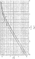
- Figs. 6-7 illustrate how the input power vs output power relationship is influenced by different ways of biasing the bulk node 120n, 120p of the differential pair of NMOS transistors 100n, 100p in Fig. 4 according to simulation examples. It should be noted that the quantitative results depend on process parameters for a given manufacturing process and selection of transistor dimensions. Hence, the quantitative results vary between different power amplifier designs. What is more generic is the qualitative behavior of the simulation results, discussed further below.
- Fig. 6 illustrates three different alternatives for biasing the bulk node 120n, 120p of the differential NMOS pair 100n, 100p.
- Fig. 7 illustrates the corresponding resulting input power-output power relationship.
- Fig. 6 illustrates the bias voltage of the bulk node 120n, 120p as a function of the input power, which itself is proportional to the square of the envelope. It should be noted that a logarithmic (dBm) scale is used for the input power in Fig. 6 .
- the bias voltage is set constant to 3.0 V (labeled V 1 ) and 2.5 V (labeled V 2 ), respectively.
- the corresponding input power-output power relationships are labeled P 1 and P 2 , respectively, in Fig.
- the bias voltage varies nonlinearly with the envelope of the input signal between the (constant) V 2 curve, for low input powers, and the (also constant) V 1 curve for higher input powers.
- the bias voltage according to the V 3 curve has a quadratic dependence on the envelope (until it hits the V 1 curve).
- the corresponding input power-output power relationship is labeled P 3 in Fig. 7 . From a pure ocular inspection of the curves in Fig. 7 , it can be deduced that, using the dynamic bias voltage given by the V 3 curve in Fig. 6 results in an increased compression point compared with both of the constant alternatives V 1 and V 2 .
- the V 3 curve in Fig. 6 starts at a first voltage (2.5 V) for low values of the envelope and increases towards a second value (3.0 V) with increasing envelope.
- the nonlinear function can be described as an increasing function generating a first voltage at a first envelope level and a second higher voltage at a second higher envelope level. It can also be observed from Fig. 6 that the rate of increase of the V 3 curve increases for an increasing envelope, such that the curve "bends upwards" towards the second voltage level. Mathematically, this can be expressed in terms of that the increasing nonlinear function is a convex function.
- the at least one transistor 100, 100n, 100p is an NMOS transistor
- the nonlinear function is an increasing convex function between a first envelope level and a second, higher, envelope level.
- a corresponding nonlinear curve i.e. corresponding to V 3
- V 3 a corresponding nonlinear curve
- the nonlinear function is a decreasing concave function between a first envelope level and a second, higher, envelope level.
- the bias-voltage generation circuit 130 is an analog circuit. An example of this is provided in Fig. 8 , showing a circuit schematic. As illustrated in Fig. 8 , the bias-voltage generation circuit 130 may comprise a rectifier circuit 200 configured to generate a rectified input voltage. In the example illustrated in Fig. 8 , the rectifier circuit 200 comprises differential transistor pair 210n, 210p. The transistor 210n is configured to receive the negative component of the differential input voltage at its gate terminal. Similarly, the transistor 210p is configured to receive the positive component of the differential input voltage at its gate terminal. Furthermore, in Fig.
- the transistors 210n, 210p have their drain terminals connected to a common node, to which a bias current source 220 is also connected for providing a bias current.
- the rectified input voltage is generated at said common node.
- This type of rectifier circuit has an inherent nonlinearity that can be utilized to generate the dynamic bias voltage as a nonlinear function of the envelope of the input signal. It should be noted that other rectifier topologies than that illustrated in Fig. 8 can be used as well, e.g. rectifier topologies using diode bridges, etc.
- the bias voltage generation circuit 130 comprises an amplifier circuit 230 operatively connected to the rectifier circuit 200 and configured to generate the dynamic bias voltage based on the rectified input voltage.
- the bias voltage generation circuit 130 may optionally comprise a filter circuit 240 connected between the rectifier circuit 200 and the amplifier circuit 230.
- the filter circuit 240 may be configured to suppress high-frequency content of the rectified input voltage, such as components at the radio frequency (RF) and harmonics thereof, while passing lower-frequency content of the rectified input voltage corresponding to the envelope of the input signal.
- the filter 240 may, for instance, be implemented as a simple RC-link, comprising a resistor 250 and a capacitor 260.
- Figs. 9-10 illustrates how the gain A of the amplifier 230, shown in Fig. 8 , can influence the linearity of the power amplifier 20 according to simulation examples.
- the quantitative results depend on process parameters for a given manufacturing process and selection of transistor dimensions. Hence, again, the quantitative results vary between different power amplifier designs. What is more generic is the qualitative behavior of the simulation results, discussed further below.
- Fig. 9 shows the derivative of the power, in logarithmic scale, of the fundamental tone with respect to the input power, also in logarithmic scale.
- P out log log 10
- P out log the output power in logarithmic scale and P in log is the input power in logarithmic scale.
- said derivative is 1 for all input power levels.
- the 10 logarithm was used above as an example, but it is readily understood that the ideal derivative would be 1 regardless of what logarithm is used, or for instance if the powers, in logarithmic scale, are expressed in a "dB unit" such as dBm.
- Fig. 9 the ideal value of 1 is indicated in the plot as well for reference.
- the amplifier circuit 230 may be a variable-gain amplifier (VGA) circuit.
- the power amplifier 20 may further comprise a control circuit configured to tune the gain of the amplifier circuit 230.
- An example is illustrated in Fig. 11 .
- the power amplifier 20 comprises a control circuit 300 configured to tune the gain of the amplifier circuit 230.
- the control circuit 300 may, for instance, be configured to measure the signal output from the power amplifier 20, as illustrated with an arrow from the antenna 25 to the control circuit 300 in Fig. 11 , e.g.
- the control unit 300 may e.g. comprise a transmitter observation receiver (TOR) configured to measure the signal output from the power amplifier 20. Furthermore, the control unit 300 may be configured to adjust the gain of the VGA 130 to reduce the observed metric of nonlinearity. For example, the control unit 300 may be configured to test a number of gain settings and select the one that gives the best nonlinearity metric, e.g. the lowest IM3 product.
- TOR transmitter observation receiver
- control unit 300 may be configured to test a gain setting that is slightly higher than the current gain setting and a gain setting that is slightly lower than the current gain setting, and thereby be able to determine whether the gain should be increased or decreased, or potentially left as is. This process may be iterated as needed, e.g. at regular intervals, or when the control unit 300 observes that an adjustment is needed, e.g. because the measured nonlinearity metric exceeds a threshold.
- the dynamic bias voltage is generated by means of digital signal processing and converted to an analog voltage by means of a digital-to-analog converter.
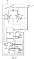
- An embodiment of the invention is illustrated in Fig. 12 .
- the bias-voltage generation circuit 130 comprises a digital signal-processing circuit 350.
- the digital signal-processing circuit 350 is configured to apply the nonlinear function, to the envelope, in the digital domain to generate a digital bias signal.
- the bias-voltage generation unit 130 comprises a digital-to-analog converter 360.
- the digital-to-analog converter 360 is configured to convert the digital bias signal to the analog domain to generate the dynamic bias voltage.
- the digital signal processing circuit 350 is configured to measure the signal output from the power amplifier 20, e.g. in order to estimate or determine the IM3 product of the signal output from the power amplifier 20, or some other metric of the nonlinearity of the power amplifier 20. This is similar to what is presented above regarding the control unit 300 in Fig. 11 .
- the digital signal-processing circuit 350 may e.g. comprise a TOR configured to measure the signal output from the power amplifier 20.
- the digital signal-processing circuit 350 is configured to adjust coefficients of nonlinear function, such as the coefficients a j mentioned above, to reduce the observed metric of nonlinearity.
- the digital signal-processing circuit 350 may be configured to test a number of coefficient settings and select the one that gives the best nonlinearity metric, e.g. the lowest IM3 product.
- the digital signal-processing circuit 350 may be configured to test coefficient settings in a neighborhood of a current coefficient setting e.g. according to some gradient or steepest descent method, and thereby be able to determine in what direction to adjust the coefficients, or potentially leave them as they are. This process may be iterated as needed, e.g. at regular intervals, or when the digital signal-processing circuit 350 observes that an adjustment is needed, e.g. because the measured nonlinearity metric exceeds a threshold.
- the envelope can be derived in the digital domain from the baseband signal.
- the digital signal processing circuit 350 is configured to derive the envelope in the digital domain from the digital baseband signal.
- the digital signal-processing circuit 350 may e.g. be configured to receive the digital baseband signal from a digital baseband processor (not shown) of the transmitter circuit 10.
- the digital signal processing circuit 350 is configured to receive the envelope from the digital baseband circuit.
- the digital signal-processing circuit 350 is, or is comprised in, said digital baseband processor.
- the digital signal processing circuit 350 may be configured to derive the envelope from the RF signal input to the inputs "in” ( Fig. 3 ) or “inn” and “inp” ( Figs. 4 and 12 ) of the power amplifier.
- the digital signal processing circuit 350 may comprise one or more analog-to-digital converters (not shown) configured to digitize the RF signal.
- the digital signal-processing circuit 350 may be configured to derive the envelope from the digitized RF signal.
- the transistors 100, 100n, and 100p may be advantageously fabricated in a silicon-on-insulator manufacturing process technology.
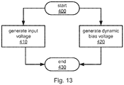
- Step 410 comprises generating the input voltage as a linear function of an input signal, as has been described above with reference to the power amplifier 20.
- Step 420 comprises generating, e.g. by the bias-voltage generation circuit 130, the dynamic bias voltage as a nonlinear function of an envelope of the input signal, as has been described above with reference to the power amplifier 20.
Landscapes
- Engineering & Computer Science (AREA)
- Power Engineering (AREA)
- Physics & Mathematics (AREA)
- Nonlinear Science (AREA)
- Microelectronics & Electronic Packaging (AREA)
- Computer Networks & Wireless Communication (AREA)
- Signal Processing (AREA)
- Amplifiers (AREA)
Description
- The present invention relates to a power amplifier.
- Power amplifiers are used in basically all wireless communication systems. One of the key parameters of a power amplifier is its linearity and compression point. Nonlinear transfer function of an amplifier will create intermodulation products and harmonic distortion. In general terms amplifiers can be linearized using a few methods, which are; negative feedback, increased bias to signal ratio, error feed forward and predistortion. If the nonlinearity is known, then predistortion can be used to linearize it. Digital predistortion of the transmitted signal is commonly used to linearize the output in cellular systems.
- Some integrated circuit manufacturing process technologies allows the bulk terminal, or back-gate terminal, of individual transistors to be biased individually. An example of this is in the context of power amplifiers is presented in M. R. Ghajar et al "Backgate Modulation Technique for Higher Efficiency Envelope Tracking", IEEE Transactions on Microwave Theory and Techniques, vol. 61, no. 4, pp. 1599-1607, April 2013. One such type of manufacturing process technology is commonly referred to as silicon-on-insulator (SOI) technology, wherein transistors are formed in a thin layer of silicon on top of a substrate of an insulating material.
-
US 2003/076172 A1 discloses an amplifier circuit and method that can be used to save power or reduce distortion in an electronic system, such as a wireless communication system. The amplifier circuit comprises a transistor having a gate terminal, drain terminal, body terminal, and a load. An input signal has different signal envelopes during different time periods. A control signal coupled to the body terminal is used to change the voltage on the body terminal when the input receives different envelopes. Accordingly, the amplifier can be biased to use less power when lower envelopes are being received. Electronic systems, such as wireless communication systems, can realize advantageous performance enhancements by utilizing the amplifier and other techniques employed by embodiments of the present invention. -
US 2016/276982 A1 discloses a power amplifier including an amplifier including at least one field effect transistor (FET) that operates in an amplifying stage configured to amplify an input signal, and a body controller configured to control a bias voltage of a body terminal of the FET based on a power of the input signal. The body controller performs controlling so that the bias voltage of the body terminal is reduced in response to the power of the input signal being increased. Accordingly, such a power amplifier exhibits improved linearity. -
US 6,127,892 A discloses an amplification circuit that comprises an MOS transistor having a gate receiving an amplified signal, a source electrically connected to ground, and a drain electrically connected to a supply voltage, wherein the back gate-source voltage of the MOS transistor is made larger as the gate-source voltage of the MOS transistor becomes larger, thereby making the threshold voltage of the MOS transistor smaller. -
US 7,893,766 B1 discloses a method and apparatus for extending the common mode range of a differential amplifier. A circuit has a common mode detection circuit, a common mode voltage inversion circuit, and a differential amplifier. The common mode detection circuit receives a differential signal and detects a common mode voltage. The common mode voltage inversion circuit is coupled to the common mode detection circuit. The common mode voltage inversion circuit has an input node that receives the common mode voltage and an output node that outputs body voltage, wherein the common mode voltage inversion circuit creates an inverse relationship between the common mode voltage and the body voltage. The differential amplifier includes a differential pair of transistors that have a pair of body terminals coupled to the output node of the common mode voltage inversion circuit. - The inventors have realized that linearization of a power amplifier can be facilitated in an efficient way by driving the bulk node of an input transistor of the power amplifier with a dynamic bias voltage, which is a nonlinear function of the envelope of the input signal of the power amplifier. In addition, doing so enables a relatively high compression point of the power amplifier.
- According to a first aspect, there is provided a power amplifier for a transmitter circuit in accordance with the appended
independent apparatus claim 1 and a method for controlling a power amplifier for a transmitter in appended independent method claim 9. Preferred embodiments are set out in the appended dependent claims. - It should be emphasized that the term "comprises/comprising" when used in this specification is taken to specify the presence of stated features, integers, steps, or components, but does not preclude the presence or addition of one or more other features, integers, steps, components, or groups thereof.
- Further objects, features and advantages of embodiments of the invention will appear from the following detailed description, reference being made to the accompanying drawings, in which:
-
Fig. 1 illustrates a communication environment. -
Fig. 2 illustrates a transmitter circuit. -
Figs. 3-4 illustrate examples of a power amplifier not covered by the scope of protection of the invention but useful for understanding the invention. -
Fig. 5 is a signal plot. -
Figs. 6-7 show plots of simulation results. -
Fig. 8 illustrates an example of a power amplifier not covered by the scope of protection of the invention but useful for understanding the invention. -
Figs. 9-10 show plots of simulation results. -
Fig. 11 illustrates an example of a power amplifier not covered by the scope of protection of the invention but useful for understanding the invention. -
Fig. 12 illustrates an embodiment of a power amplifier according to the present invention. -
Fig. 13 is a flowchart. -
Fig. 1 illustrates a communication environment wherein embodiments of the present invention may be employed. Awireless terminal 1 of a cellular communications system is in wireless communication with aradio base station 2 of the cellular communications system. Thewireless terminal 1 may be what is generally referred to as a user equipment (UE). Thewireless terminal 1 is depicted inFig. 1 as a mobile phone, but may be any kind of device with cellular communication capabilities, such as a tablet or laptop computer, machine-type communication (MTC) device, or similar. Furthermore, a cellular communications system is used as an example throughout this disclosure. However, embodiments of the present invention may be applicable in other types of systems as well, such as but not limited to WiFi systems. - The
radio base station 2 andwireless terminal 1 are examples of what in this disclosure is generically referred to as communication apparatuses. Embodiments are described below in the context of a communication apparatus in the form of theradio base station 2 orwireless terminal 1. However, other types of communication apparatuses can be considered as well, such as a WiFi access point or WiFi enabled device. -
Fig. 2 schematically illustrates atransmitter circuit 10, which may for instance be comprised in a communication apparatus such as thewireless terminal 1 orradio base station 2. It comprises apower amplifier 20 configured to feed a signal to be transmitted to atransmission antenna 25 of the communication apparatus. Thepower amplifier 20 may be preceded by various different circuitry, well known in the art of radio transmitter design, and the present disclosure is not limited to any particular such circuitry, as illustrated by the dotted line inFig. 2 . -
Fig. 3 illustrates an example of thepower amplifier 20 not covered by the scope of protection of the invention but useful for understanding the invention. It comprises a field-effect transistor 100. InFig. 3 , the illustrated field-effect transistor 100 is an NMOS transistor. In other examples, the field-effect transistor 100 may e.g. be a PMOS transistor. The field-effect transistor 100 is configured to receive an input voltage at itsgate terminal 110 and a dynamic bias voltage at itsbulk terminal 120. InFig. 3 , thegate terminal 110 of the field-effect transistor 100 is connected to an input "in" to receive the input voltage. InFig. 3 , thepower amplifier 20 comprises a bias-voltage generation circuit 130, which is configured to generate the dynamic bias voltage. InFig. 3 , the source node of the field-effect transistor 100 is grounded and the drain node of the field-effect transistor 100 is connected via atransformer 140 to theantenna 25. However, other configurations are possible as well. - In
Fig. 3 , thepower amplifier 20 comprises a single field-effect transistor 100. That is,Fig. 3 shows a single-endedpower amplifier 20. More generically, thepower amplifier 20 comprises at least one field-effect transistor configured to receive an input voltage at the gate terminal and a dynamic bias voltage at the bulk terminal.Fig. 4 illustrates an example, not covered by the scope of protection of the invention but useful for understanding the invention, where the at least one field-effect transistor is a differential pair of field-effect transistors Fig. 4 thus shows adifferential power amplifier 20. InFig. 4 , thegate terminal 110n of the field-effect transistor 100n is connected to a negative input "inn" to receive a negative component of the differential input voltage. Similarly, inFig. 4 , thegate terminal 110p of the field-effect transistor 100p is connected to a positive input "inp" to receive a positive component of the differential input voltage. Furthermore, inFig. 4 , thebulk terminals effect transistors Fig. 4 , the source nodes of the field-effect transistors effect transistors differential transformer 140 to theantenna 25. However, other configurations are possible as well. -
Fig. 5 illustrates an example of an amplitude-modulated oscillating signal, which may be an input signal to thepower amplifier 20. This signal is labeled "signal" in the figure.Fig. 5 also illustrates the envelope (labeled "envelope") of the amplitude-modulated oscillating signal. The input voltage to the power amplifier 20 (e.g. the single-ended input voltage ofFig. 3 or differential input voltage ofFig. 4 ) is a linear function of an input signal. Furthermore, the bias-voltage generation circuit 130 is configured to generate the dynamic bias voltage as a function of the envelope of the input signal. - The gain of a power amplifier is ideally linear up the point when the amplifier saturates. However, prior to saturating in power, the amplifier typically starts dropping in gain. At some input power the gain is 1dB lower than the ideal curve. This point is called the 1dB compression point. By varying the dynamic bias voltage applied to the
bulk node effect transistor effect transistor - According to embodiments, the at least one field-
effect transistor bulk node effect transistor bulk node - The inventors have realized that if the bulk node voltage varies as a linear function of the envelope, there is a relatively high risk that either the bulk node voltage is increased too early as input power goes up, which will introduce problems with gain expansion for lower input power, or too late for higher input powers, which would lead to insufficient compensation of the gain at higher input powers in order to significantly improve the 1 dB compression point. In this context, we consider a voltage V to vary linearly with the envelope e if it can be expressed as V = c ▪ e + V offset, where V offset is a constant voltage and c is a constant. It can be noted that the zero reference electrical potential level can always be selected such that V offset = 0, i.e. V = c ▪ e. The inventors have further realized that by allowing the dynamic bias voltage to vary as a nonlinear function of the envelope, the threshold voltage can be increased early enough, for increasing input power, to significantly improve the 1 dB compression point, while avoiding the above-mentioned gain expansion for lower input powers. Therefore, according to embodiments, the bias-
voltage generation circuit 130 is configured to generate the dynamic bias voltage as a nonlinear function of the envelope of the input signal. -
Figs. 6-7 illustrate how the input power vs output power relationship is influenced by different ways of biasing thebulk node NMOS transistors Fig. 4 according to simulation examples. It should be noted that the quantitative results depend on process parameters for a given manufacturing process and selection of transistor dimensions. Hence, the quantitative results vary between different power amplifier designs. What is more generic is the qualitative behavior of the simulation results, discussed further below. -
Fig. 6 illustrates three different alternatives for biasing thebulk node differential NMOS pair Fig. 7 illustrates the corresponding resulting input power-output power relationship.Fig. 6 illustrates the bias voltage of thebulk node Fig. 6 . According to a first and a second example, the bias voltage is set constant to 3.0 V (labeled V1) and 2.5 V (labeled V2), respectively. The corresponding input power-output power relationships are labeled P1 and P2, respectively, inFig. 7 . According to a third example, labeled V3 inFig. 6 , the bias voltage varies nonlinearly with the envelope of the input signal between the (constant) V2 curve, for low input powers, and the (also constant) V1 curve for higher input powers. InFig. 6 , the bias voltage according to the V3 curve has a quadratic dependence on the envelope (until it hits the V1 curve). The corresponding input power-output power relationship is labeled P3 inFig. 7 . From a pure ocular inspection of the curves inFig. 7 , it can be deduced that, using the dynamic bias voltage given by the V3 curve inFig. 6 results in an increased compression point compared with both of the constant alternatives V1 and V2. - The V3 curve in
Fig. 6 starts at a first voltage (2.5 V) for low values of the envelope and increases towards a second value (3.0 V) with increasing envelope. Hence, the nonlinear function can be described as an increasing function generating a first voltage at a first envelope level and a second higher voltage at a second higher envelope level. It can also be observed fromFig. 6 that the rate of increase of the V3 curve increases for an increasing envelope, such that the curve "bends upwards" towards the second voltage level. Mathematically, this can be expressed in terms of that the increasing nonlinear function is a convex function. Hence, in accordance with some embodiments, wherein the at least onetransistor - For embodiments wherein the at least one
transistor transistor - According to an example not covered by the scope of protection of the invention but useful for understanding the invention, the bias-
voltage generation circuit 130 is an analog circuit. An example of this is provided inFig. 8 , showing a circuit schematic. As illustrated inFig. 8 , the bias-voltage generation circuit 130 may comprise arectifier circuit 200 configured to generate a rectified input voltage. In the example illustrated inFig. 8 , therectifier circuit 200 comprisesdifferential transistor pair transistor 210n is configured to receive the negative component of the differential input voltage at its gate terminal. Similarly, thetransistor 210p is configured to receive the positive component of the differential input voltage at its gate terminal. Furthermore, inFig. 8 , thetransistors current source 220 is also connected for providing a bias current. The rectified input voltage is generated at said common node. This type of rectifier circuit has an inherent nonlinearity that can be utilized to generate the dynamic bias voltage as a nonlinear function of the envelope of the input signal. It should be noted that other rectifier topologies than that illustrated inFig. 8 can be used as well, e.g. rectifier topologies using diode bridges, etc. Furthermore, inFig. 8 , the biasvoltage generation circuit 130 comprises anamplifier circuit 230 operatively connected to therectifier circuit 200 and configured to generate the dynamic bias voltage based on the rectified input voltage. - As illustrated in
Fig. 8 , the biasvoltage generation circuit 130 may optionally comprise afilter circuit 240 connected between therectifier circuit 200 and theamplifier circuit 230. Thefilter circuit 240 may be configured to suppress high-frequency content of the rectified input voltage, such as components at the radio frequency (RF) and harmonics thereof, while passing lower-frequency content of the rectified input voltage corresponding to the envelope of the input signal. As illustrated inFig. 8 , thefilter 240 may, for instance, be implemented as a simple RC-link, comprising aresistor 250 and acapacitor 260. -
Figs. 9-10 illustrates how the gain A of theamplifier 230, shown inFig. 8 , can influence the linearity of thepower amplifier 20 according to simulation examples. As mentioned above with reference toFigs. 6-7 , it should be noted that the quantitative results depend on process parameters for a given manufacturing process and selection of transistor dimensions. Hence, again, the quantitative results vary between different power amplifier designs. What is more generic is the qualitative behavior of the simulation results, discussed further below. -
Fig. 9 shows the derivative of the power, in logarithmic scale, of the fundamental tone with respect to the input power, also in logarithmic scale. For an ideal power amplifier, the output power, in linear scale, is proportional to the input power in linear scale, i.e.


Fig. 9 , the ideal value of 1 is indicated in the plot as well for reference. The plot labeled A = 0 corresponds to a static, constant, bulk bias voltage, following the V1 curve inFig. 6 . We refer to this as an uncompensated case. The curves labeled A = 2 and A = 4 show the simulation results when the gain of theamplifier 230 is 2 and 4, respectively. As can be seen, up to, and slightly above, 0 dBm of input power, the cases with A = 2 and A = 4 are both closer to the ideal curve than the uncompensated case. For A = 2, the curve is below the ideal curve, and for A = 4, the curve is above the ideal curve. Hence, for any value of A between 2 and 4, the result would be closer to the ideal curve than the uncompensated case (for input powers up to and slightly above 0 dBm). The best result, depending on what metric is used to determine closeness to the ideal curve, is achieved for some value of A between 2 and 4. -
Fig. 10 show similar plots for the third-order intermodulation (IM3) product. From these plots, it can be observed that for A = 2 and A = 4, the IM3 product is about 5-10 dB lower than for the uncompensated case, again for input power up to and slightly above 0 dBm. - To facilitate fine tuning of the performance of examples of the
power amplifier 20, not covered by the scope of protection of the invention but useful for understanding the invention, theamplifier circuit 230 may be a variable-gain amplifier (VGA) circuit. Thepower amplifier 20 may further comprise a control circuit configured to tune the gain of theamplifier circuit 230. An example is illustrated inFig. 11 . InFig. 11 , thepower amplifier 20 comprises acontrol circuit 300 configured to tune the gain of theamplifier circuit 230. Thecontrol circuit 300 may, for instance, be configured to measure the signal output from thepower amplifier 20, as illustrated with an arrow from theantenna 25 to thecontrol circuit 300 inFig. 11 , e.g. in order to estimate or determine the IM3 product of the signal output from thepower amplifier 20, or some other metric of the nonlinearity of thepower amplifier 20. Thecontrol unit 300 may e.g. comprise a transmitter observation receiver (TOR) configured to measure the signal output from thepower amplifier 20. Furthermore, thecontrol unit 300 may be configured to adjust the gain of theVGA 130 to reduce the observed metric of nonlinearity. For example, thecontrol unit 300 may be configured to test a number of gain settings and select the one that gives the best nonlinearity metric, e.g. the lowest IM3 product. For instance, thecontrol unit 300 may be configured to test a gain setting that is slightly higher than the current gain setting and a gain setting that is slightly lower than the current gain setting, and thereby be able to determine whether the gain should be increased or decreased, or potentially left as is. This process may be iterated as needed, e.g. at regular intervals, or when thecontrol unit 300 observes that an adjustment is needed, e.g. because the measured nonlinearity metric exceeds a threshold. - According to the invention, the dynamic bias voltage is generated by means of digital signal processing and converted to an analog voltage by means of a digital-to-analog converter. An embodiment of the invention is illustrated in
Fig. 12 . The bias-voltage generation circuit 130 comprises a digital signal-processing circuit 350. The digital signal-processing circuit 350 is configured to apply the nonlinear function, to the envelope, in the digital domain to generate a digital bias signal. The nonlinear function may for example be a polynomial, such as
Fig. 12 , the bias-voltage generation unit 130 comprises a digital-to-analog converter 360. The digital-to-analog converter 360 is configured to convert the digital bias signal to the analog domain to generate the dynamic bias voltage. - As indicated in
Fig. 12 with anoptional connection 370 to theantenna 25, the digitalsignal processing circuit 350 is configured to measure the signal output from thepower amplifier 20, e.g. in order to estimate or determine the IM3 product of the signal output from thepower amplifier 20, or some other metric of the nonlinearity of thepower amplifier 20. This is similar to what is presented above regarding thecontrol unit 300 inFig. 11 . The digital signal-processing circuit 350 may e.g. comprise a TOR configured to measure the signal output from thepower amplifier 20. Furthermore, the digital signal-processing circuit 350 is configured to adjust coefficients of nonlinear function, such as the coefficients aj mentioned above, to reduce the observed metric of nonlinearity. For example, the digital signal-processing circuit 350 may be configured to test a number of coefficient settings and select the one that gives the best nonlinearity metric, e.g. the lowest IM3 product. For instance, the digital signal-processing circuit 350 may be configured to test coefficient settings in a neighborhood of a current coefficient setting e.g. according to some gradient or steepest descent method, and thereby be able to determine in what direction to adjust the coefficients, or potentially leave them as they are. This process may be iterated as needed, e.g. at regular intervals, or when the digital signal-processing circuit 350 observes that an adjustment is needed, e.g. because the measured nonlinearity metric exceeds a threshold. - It should be noted that the envelope can be derived in the digital domain from the baseband signal. Hence, in some embodiments, the digital
signal processing circuit 350 is configured to derive the envelope in the digital domain from the digital baseband signal. The digital signal-processing circuit 350 may e.g. be configured to receive the digital baseband signal from a digital baseband processor (not shown) of thetransmitter circuit 10. - In some embodiments, the digital
signal processing circuit 350 is configured to receive the envelope from the digital baseband circuit. - In some embodiments, the digital signal-
processing circuit 350 is, or is comprised in, said digital baseband processor. - In other embodiments, the digital
signal processing circuit 350 may be configured to derive the envelope from the RF signal input to the inputs "in" (Fig. 3 ) or "inn" and "inp" (Figs. 4 and12 ) of the power amplifier. For example, the digitalsignal processing circuit 350 may comprise one or more analog-to-digital converters (not shown) configured to digitize the RF signal. The digital signal-processing circuit 350 may be configured to derive the envelope from the digitized RF signal. - In any of the embodiments described above, the
transistors - According to some examples useful for understanding the invention but not covered by the scope of the invention, there is provided a method for controlling the
power amplifier 20 described above. A flowchart of such a method is provided inFig. 13 . The operation of the method is commenced instep 400. Inparallel steps power amplifier 20 and the dynamic bias voltage are simultaneously generated continually, until the operation is ended in step 430. Step 410 comprises generating the input voltage as a linear function of an input signal, as has been described above with reference to thepower amplifier 20. Step 420 comprises generating, e.g. by the bias-voltage generation circuit 130, the dynamic bias voltage as a nonlinear function of an envelope of the input signal, as has been described above with reference to thepower amplifier 20.
Claims (9)
- A power amplifier (20) for a transmitter circuit (10), the power amplifier (20) comprising:at least one field-effect transistor (100, 100n, 100p) having a gate terminal (110, 110n, 110p) and a bulk terminal (120, 120n, 120p), wherein the at least one field-effect transistor (100, 100n, 100p) is configured to receive an input voltage at the gate terminal (110, 110n, 110p) and a dynamic bias voltage at the bulk terminal (120, 120n, 120p); anda bias-voltage generation circuit (130); wherein:wherein the bias-voltage generation circuit (130) comprises:the input voltage is a linear function of an input signal; andthe bias-voltage generation circuit (130) is configured to generate the dynamic bias voltage as a nonlinear function of an envelope of the input signal;a digital signal-processing circuit (350) configured to apply the nonlinear function in a digital domain to generate a digital bias signal;a digital-to-analog converter (360) configured to convert the digital bias signal to an analog domain to generate the dynamic bias voltage;characterized in that the digital signal-processing circuit (350) is configured to:measure a signal output from the power amplifier (20) to determine a metric of nonlinearity of the power amplifier (20); andadjust coefficients of the nonlinear function when the determined metric of nonlinearity exceeds a threshold.
- The power amplifier (20) according to claim 1, wherein either:the at least one field-effect transistor (100, 100n, 100p) is an NMOS transistor and the nonlinear function is an increasing convex function between a first envelope level and a second, higher, envelope level; orthe at least one field-effect transistor (100, 100n, 100p) is a PMOS transistor and the nonlinear function is a decreasing concave function between a first envelope level and a second, higher, envelope level.
- The power amplifier (20) according to any preceding claim, wherein the at least one field-effect transistor (100, 100n, 100p) is fabricated in a silicon-on-insulator process technology.
- The power amplifier (20) according to any preceding claim, wherein the at least one field-effect transistor (100, 100n, 100p) is a differential pair of field-effect transistors.
- A transmitter circuit (10) comprising the power amplifier (20) according to any one of claims 1-4.
- A communication apparatus (1, 2) comprising the transmitter circuit (10) according to claim 5.
- The communication apparatus (1, 2) according to claim 6, wherein the communication apparatus (1) is a wireless terminal for a cellular communication system.
- The communication apparatus (1, 2) according to claim 6, wherein the communication apparatus (2) is a radio base station for a cellular communication system.
- A method of controlling a power amplifier (20) for a transmitter circuit (10), wherein the power amplifier (20) comprises at least one field-effect transistor (100, 100n, 100p) having a gate terminal (110, 110n, 110p) and a bulk terminal (120, 120n, 120p), wherein the at least one field-effect transistor (100, 100n, 100p) is configured to receive an input voltage at the gate terminal (110, 110n, 110p) and a dynamic bias voltage at the bulk terminal (120, 120n, 120p), and wherein the method comprises:generating (410) the input voltage as a linear function of an input signal; andgenerating (420) by means of a bias-voltage generation circuit (130) the dynamic bias voltage as a nonlinear function of an envelope of the input signal, wherein the bias-voltage generation circuit (130) comprises a digital signal-processing circuit (350) configured to apply the nonlinear function in a digital domain to generate a digital bias signal and a digital-to-analog converter (360) configured to convert the digital bias signal to an analog domain to generate the dynamic bias voltage; andcharacterized in that the method comprises:measuring, by means of the digital signal-processing unit (350), a signal output from the power amplifier (20) to determine a metric of nonlinearity of the power amplifier (20); andadjusting, by means of the digital signal-processing unit (350), coefficients of the nonlinear function when the determined metric of nonlinearity exceeds a threshold.
Applications Claiming Priority (1)
| Application Number | Priority Date | Filing Date | Title |
|---|---|---|---|
| PCT/EP2016/074799 WO2018068871A1 (en) | 2016-10-14 | 2016-10-14 | Power amplifier |
Publications (2)
| Publication Number | Publication Date |
|---|---|
| EP3526897A1 EP3526897A1 (en) | 2019-08-21 |
| EP3526897B1 true EP3526897B1 (en) | 2021-06-30 |
Family
ID=57136907
Family Applications (1)
| Application Number | Title | Priority Date | Filing Date |
|---|---|---|---|
| EP16781814.5A Active EP3526897B1 (en) | 2016-10-14 | 2016-10-14 | Power amplifier |
Country Status (3)
| Country | Link |
|---|---|
| US (2) | US10848108B2 (en) |
| EP (1) | EP3526897B1 (en) |
| WO (1) | WO2018068871A1 (en) |
Families Citing this family (2)
| Publication number | Priority date | Publication date | Assignee | Title |
|---|---|---|---|---|
| CA3154262A1 (en) | 2019-09-13 | 2021-03-18 | Socovar S.E.C. | Power amplifier linearizing module and power amplifier system equipped therewith |
| WO2023245527A1 (en) | 2022-06-23 | 2023-12-28 | Telefonaktiebolaget Lm Ericsson (Publ) | Radio resource allocation in a communication network |
Family Cites Families (14)
| Publication number | Priority date | Publication date | Assignee | Title |
|---|---|---|---|---|
| US3800802A (en) * | 1972-01-07 | 1974-04-02 | Int Medical Electronics Ltd | Short-wave therapy apparatus |
| US5420536A (en) * | 1993-03-16 | 1995-05-30 | Victoria University Of Technology | Linearized power amplifier |
| JPH11317628A (en) | 1998-05-07 | 1999-11-16 | Mitsubishi Electric Corp | Amplifier circuit |
| US6784744B2 (en) * | 2001-09-27 | 2004-08-31 | Powerq Technologies, Inc. | Amplifier circuits and methods |
| US7421254B2 (en) * | 2003-10-23 | 2008-09-02 | Broadcom Corporation | High linearity, high efficiency power amplifier with DSP assisted linearity optimization |
| US7787839B2 (en) * | 2006-12-06 | 2010-08-31 | Broadcom Corporation | RFIC with dynamically controlled power amplifier |
| TWI332747B (en) * | 2006-12-13 | 2010-11-01 | Univ Nat Taiwan | Bias circuits and signal amplifier circuits |
| JP4808182B2 (en) * | 2007-04-27 | 2011-11-02 | 株式会社エヌ・ティ・ティ・ドコモ | Wireless communication apparatus and power supply method for wireless communication apparatus |
| US8416898B1 (en) * | 2009-06-11 | 2013-04-09 | Altera Corporation | Techniques for decision feedback equalization that reduce variations in the tap weight |
| US7893766B1 (en) * | 2009-09-10 | 2011-02-22 | International Business Machines Corporation | Adaptive common mode bias for differential amplifier input circuits |
| US8111104B2 (en) * | 2010-01-25 | 2012-02-07 | Peregrine Semiconductor Corporation | Biasing methods and devices for power amplifiers |
| KR102000759B1 (en) * | 2014-02-24 | 2019-07-17 | 삼성전기주식회사 | Adaptive bias circuit and power amplifier |
| US9559646B2 (en) * | 2014-09-10 | 2017-01-31 | Samsung Electronics Co., Ltd | Apparatus and method for dynamically biased baseband current amplifier |
| KR102117470B1 (en) * | 2015-03-18 | 2020-06-03 | 삼성전기주식회사 | Power amplifier |
-
2016
- 2016-10-14 WO PCT/EP2016/074799 patent/WO2018068871A1/en not_active Ceased
- 2016-10-14 EP EP16781814.5A patent/EP3526897B1/en active Active
- 2016-10-14 US US16/340,503 patent/US10848108B2/en active Active
-
2020
- 2020-10-13 US US17/069,355 patent/US11228285B2/en active Active
Non-Patent Citations (1)
| Title |
|---|
| None * |
Also Published As
| Publication number | Publication date |
|---|---|
| US20190245493A1 (en) | 2019-08-08 |
| US20210028749A1 (en) | 2021-01-28 |
| US11228285B2 (en) | 2022-01-18 |
| US10848108B2 (en) | 2020-11-24 |
| WO2018068871A1 (en) | 2018-04-19 |
| EP3526897A1 (en) | 2019-08-21 |
Similar Documents
| Publication | Publication Date | Title |
|---|---|---|
| US7696826B2 (en) | Temperature compensation of collector-voltage control RF amplifiers | |
| EP3322097B1 (en) | Envelope tracking apparatus and method | |
| US20140266432A1 (en) | Amplifier phase distortion correction based on amplitude distortion measurement | |
| US8217716B2 (en) | Bias circuit, high-power amplifier, and portable information terminal | |
| US10298191B2 (en) | Power amplifier module | |
| US12283925B2 (en) | Bias circuit and power amplifier circuit | |
| US20140253243A1 (en) | Power amplifying module | |
| US20020021173A1 (en) | Non-linear distortion compensating apparatus | |
| US11228285B2 (en) | Power amplifier | |
| JPH09246873A (en) | Distortion compensation circuit | |
| KR101766628B1 (en) | Transmitter with predistorter | |
| US10008986B2 (en) | Power amplification apparatus and method for controlling power amplification apparatus | |
| KR100281647B1 (en) | RF integrated circuit for small signal linearity improvement using active element balun | |
| US20140010330A1 (en) | Transmission device and transmission method | |
| EP1709731B1 (en) | Electronic circuit | |
| JP5983968B2 (en) | Power amplification circuit and power amplification module | |
| JP3487060B2 (en) | Distortion compensation circuit | |
| US20220393655A1 (en) | Linearization using complementary devices | |
| US12489409B2 (en) | Power amplifier | |
| JP2011015239A (en) | Amplifier circuit, and method of adjusting bias used for the same | |
| KR100320427B1 (en) | Method and Device for Compensation of Distortion Signal in Communication System | |
| JP3361350B2 (en) | Power amplifier | |
| JPH0715247A (en) | Power amplifier | |
| JP3406634B2 (en) | Power amplifier | |
| KR20060116882A (en) | Distortion signal compensation device in communication system |
Legal Events
| Date | Code | Title | Description |
|---|---|---|---|
| STAA | Information on the status of an ep patent application or granted ep patent |
Free format text: STATUS: THE INTERNATIONAL PUBLICATION HAS BEEN MADE |
|
| PUAI | Public reference made under article 153(3) epc to a published international application that has entered the european phase |
Free format text: ORIGINAL CODE: 0009012 |
|
| STAA | Information on the status of an ep patent application or granted ep patent |
Free format text: STATUS: REQUEST FOR EXAMINATION WAS MADE |
|
| 17P | Request for examination filed |
Effective date: 20190326 |
|
| AK | Designated contracting states |
Kind code of ref document: A1 Designated state(s): AL AT BE BG CH CY CZ DE DK EE ES FI FR GB GR HR HU IE IS IT LI LT LU LV MC MK MT NL NO PL PT RO RS SE SI SK SM TR |
|
| AX | Request for extension of the european patent |
Extension state: BA ME |
|
| DAV | Request for validation of the european patent (deleted) | ||
| DAX | Request for extension of the european patent (deleted) | ||
| STAA | Information on the status of an ep patent application or granted ep patent |
Free format text: STATUS: EXAMINATION IS IN PROGRESS |
|
| 17Q | First examination report despatched |
Effective date: 20200810 |
|
| GRAP | Despatch of communication of intention to grant a patent |
Free format text: ORIGINAL CODE: EPIDOSNIGR1 |
|
| STAA | Information on the status of an ep patent application or granted ep patent |
Free format text: STATUS: GRANT OF PATENT IS INTENDED |
|
| INTG | Intention to grant announced |
Effective date: 20210419 |
|
| GRAS | Grant fee paid |
Free format text: ORIGINAL CODE: EPIDOSNIGR3 |
|
| GRAA | (expected) grant |
Free format text: ORIGINAL CODE: 0009210 |
|
| STAA | Information on the status of an ep patent application or granted ep patent |
Free format text: STATUS: THE PATENT HAS BEEN GRANTED |
|
| AK | Designated contracting states |
Kind code of ref document: B1 Designated state(s): AL AT BE BG CH CY CZ DE DK EE ES FI FR GB GR HR HU IE IS IT LI LT LU LV MC MK MT NL NO PL PT RO RS SE SI SK SM TR |
|
| REG | Reference to a national code |
Ref country code: CH Ref legal event code: EP |
|
| REG | Reference to a national code |
Ref country code: AT Ref legal event code: REF Ref document number: 1407308 Country of ref document: AT Kind code of ref document: T Effective date: 20210715 |
|
| REG | Reference to a national code |
Ref country code: DE Ref legal event code: R096 Ref document number: 602016060023 Country of ref document: DE |
|
| REG | Reference to a national code |
Ref country code: NL Ref legal event code: FP |
|
| REG | Reference to a national code |
Ref country code: IE Ref legal event code: FG4D |
|
| REG | Reference to a national code |
Ref country code: LT Ref legal event code: MG9D |
|
| PG25 | Lapsed in a contracting state [announced via postgrant information from national office to epo] |
Ref country code: FI Free format text: LAPSE BECAUSE OF FAILURE TO SUBMIT A TRANSLATION OF THE DESCRIPTION OR TO PAY THE FEE WITHIN THE PRESCRIBED TIME-LIMIT Effective date: 20210630 Ref country code: BG Free format text: LAPSE BECAUSE OF FAILURE TO SUBMIT A TRANSLATION OF THE DESCRIPTION OR TO PAY THE FEE WITHIN THE PRESCRIBED TIME-LIMIT Effective date: 20210930 Ref country code: HR Free format text: LAPSE BECAUSE OF FAILURE TO SUBMIT A TRANSLATION OF THE DESCRIPTION OR TO PAY THE FEE WITHIN THE PRESCRIBED TIME-LIMIT Effective date: 20210630 |
|
| REG | Reference to a national code |
Ref country code: AT Ref legal event code: MK05 Ref document number: 1407308 Country of ref document: AT Kind code of ref document: T Effective date: 20210630 |
|
| PG25 | Lapsed in a contracting state [announced via postgrant information from national office to epo] |
Ref country code: GR Free format text: LAPSE BECAUSE OF FAILURE TO SUBMIT A TRANSLATION OF THE DESCRIPTION OR TO PAY THE FEE WITHIN THE PRESCRIBED TIME-LIMIT Effective date: 20211001 Ref country code: LV Free format text: LAPSE BECAUSE OF FAILURE TO SUBMIT A TRANSLATION OF THE DESCRIPTION OR TO PAY THE FEE WITHIN THE PRESCRIBED TIME-LIMIT Effective date: 20210630 Ref country code: RS Free format text: LAPSE BECAUSE OF FAILURE TO SUBMIT A TRANSLATION OF THE DESCRIPTION OR TO PAY THE FEE WITHIN THE PRESCRIBED TIME-LIMIT Effective date: 20210630 Ref country code: SE Free format text: LAPSE BECAUSE OF FAILURE TO SUBMIT A TRANSLATION OF THE DESCRIPTION OR TO PAY THE FEE WITHIN THE PRESCRIBED TIME-LIMIT Effective date: 20210630 Ref country code: NO Free format text: LAPSE BECAUSE OF FAILURE TO SUBMIT A TRANSLATION OF THE DESCRIPTION OR TO PAY THE FEE WITHIN THE PRESCRIBED TIME-LIMIT Effective date: 20210930 |
|
| PG25 | Lapsed in a contracting state [announced via postgrant information from national office to epo] |
Ref country code: SM Free format text: LAPSE BECAUSE OF FAILURE TO SUBMIT A TRANSLATION OF THE DESCRIPTION OR TO PAY THE FEE WITHIN THE PRESCRIBED TIME-LIMIT Effective date: 20210630 Ref country code: SK Free format text: LAPSE BECAUSE OF FAILURE TO SUBMIT A TRANSLATION OF THE DESCRIPTION OR TO PAY THE FEE WITHIN THE PRESCRIBED TIME-LIMIT Effective date: 20210630 Ref country code: EE Free format text: LAPSE BECAUSE OF FAILURE TO SUBMIT A TRANSLATION OF THE DESCRIPTION OR TO PAY THE FEE WITHIN THE PRESCRIBED TIME-LIMIT Effective date: 20210630 Ref country code: CZ Free format text: LAPSE BECAUSE OF FAILURE TO SUBMIT A TRANSLATION OF THE DESCRIPTION OR TO PAY THE FEE WITHIN THE PRESCRIBED TIME-LIMIT Effective date: 20210630 Ref country code: PT Free format text: LAPSE BECAUSE OF FAILURE TO SUBMIT A TRANSLATION OF THE DESCRIPTION OR TO PAY THE FEE WITHIN THE PRESCRIBED TIME-LIMIT Effective date: 20211102 Ref country code: RO Free format text: LAPSE BECAUSE OF FAILURE TO SUBMIT A TRANSLATION OF THE DESCRIPTION OR TO PAY THE FEE WITHIN THE PRESCRIBED TIME-LIMIT Effective date: 20210630 Ref country code: ES Free format text: LAPSE BECAUSE OF FAILURE TO SUBMIT A TRANSLATION OF THE DESCRIPTION OR TO PAY THE FEE WITHIN THE PRESCRIBED TIME-LIMIT Effective date: 20210630 Ref country code: AT Free format text: LAPSE BECAUSE OF FAILURE TO SUBMIT A TRANSLATION OF THE DESCRIPTION OR TO PAY THE FEE WITHIN THE PRESCRIBED TIME-LIMIT Effective date: 20210630 |
|
| PG25 | Lapsed in a contracting state [announced via postgrant information from national office to epo] |
Ref country code: PL Free format text: LAPSE BECAUSE OF FAILURE TO SUBMIT A TRANSLATION OF THE DESCRIPTION OR TO PAY THE FEE WITHIN THE PRESCRIBED TIME-LIMIT Effective date: 20210630 |
|
| REG | Reference to a national code |
Ref country code: DE Ref legal event code: R097 Ref document number: 602016060023 Country of ref document: DE |
|
| PG25 | Lapsed in a contracting state [announced via postgrant information from national office to epo] |
Ref country code: DK Free format text: LAPSE BECAUSE OF FAILURE TO SUBMIT A TRANSLATION OF THE DESCRIPTION OR TO PAY THE FEE WITHIN THE PRESCRIBED TIME-LIMIT Effective date: 20210630 |
|
| PLBE | No opposition filed within time limit |
Free format text: ORIGINAL CODE: 0009261 |
|
| STAA | Information on the status of an ep patent application or granted ep patent |
Free format text: STATUS: NO OPPOSITION FILED WITHIN TIME LIMIT |
|
| REG | Reference to a national code |
Ref country code: CH Ref legal event code: PL |
|
| PG25 | Lapsed in a contracting state [announced via postgrant information from national office to epo] |
Ref country code: AL Free format text: LAPSE BECAUSE OF FAILURE TO SUBMIT A TRANSLATION OF THE DESCRIPTION OR TO PAY THE FEE WITHIN THE PRESCRIBED TIME-LIMIT Effective date: 20210630 |
|
| 26N | No opposition filed |
Effective date: 20220331 |
|
| REG | Reference to a national code |
Ref country code: BE Ref legal event code: MM Effective date: 20211031 |
|
| PG25 | Lapsed in a contracting state [announced via postgrant information from national office to epo] |
Ref country code: MC Free format text: LAPSE BECAUSE OF FAILURE TO SUBMIT A TRANSLATION OF THE DESCRIPTION OR TO PAY THE FEE WITHIN THE PRESCRIBED TIME-LIMIT Effective date: 20210630 |
|
| PG25 | Lapsed in a contracting state [announced via postgrant information from national office to epo] |
Ref country code: LU Free format text: LAPSE BECAUSE OF NON-PAYMENT OF DUE FEES Effective date: 20211014 Ref country code: IT Free format text: LAPSE BECAUSE OF FAILURE TO SUBMIT A TRANSLATION OF THE DESCRIPTION OR TO PAY THE FEE WITHIN THE PRESCRIBED TIME-LIMIT Effective date: 20210630 Ref country code: BE Free format text: LAPSE BECAUSE OF NON-PAYMENT OF DUE FEES Effective date: 20211031 |
|
| PG25 | Lapsed in a contracting state [announced via postgrant information from national office to epo] |
Ref country code: LI Free format text: LAPSE BECAUSE OF NON-PAYMENT OF DUE FEES Effective date: 20211031 Ref country code: CH Free format text: LAPSE BECAUSE OF NON-PAYMENT OF DUE FEES Effective date: 20211031 |
|
| PG25 | Lapsed in a contracting state [announced via postgrant information from national office to epo] |
Ref country code: FR Free format text: LAPSE BECAUSE OF NON-PAYMENT OF DUE FEES Effective date: 20211031 |
|
| PG25 | Lapsed in a contracting state [announced via postgrant information from national office to epo] |
Ref country code: IE Free format text: LAPSE BECAUSE OF NON-PAYMENT OF DUE FEES Effective date: 20211014 |
|
| PG25 | Lapsed in a contracting state [announced via postgrant information from national office to epo] |
Ref country code: LT Free format text: LAPSE BECAUSE OF FAILURE TO SUBMIT A TRANSLATION OF THE DESCRIPTION OR TO PAY THE FEE WITHIN THE PRESCRIBED TIME-LIMIT Effective date: 20210630 |
|
| P01 | Opt-out of the competence of the unified patent court (upc) registered |
Effective date: 20230523 |
|
| PG25 | Lapsed in a contracting state [announced via postgrant information from national office to epo] |
Ref country code: CY Free format text: LAPSE BECAUSE OF FAILURE TO SUBMIT A TRANSLATION OF THE DESCRIPTION OR TO PAY THE FEE WITHIN THE PRESCRIBED TIME-LIMIT Effective date: 20210630 |
|
| PG25 | Lapsed in a contracting state [announced via postgrant information from national office to epo] |
Ref country code: HU Free format text: LAPSE BECAUSE OF FAILURE TO SUBMIT A TRANSLATION OF THE DESCRIPTION OR TO PAY THE FEE WITHIN THE PRESCRIBED TIME-LIMIT; INVALID AB INITIO Effective date: 20161014 |
|
| PG25 | Lapsed in a contracting state [announced via postgrant information from national office to epo] |
Ref country code: MK Free format text: LAPSE BECAUSE OF FAILURE TO SUBMIT A TRANSLATION OF THE DESCRIPTION OR TO PAY THE FEE WITHIN THE PRESCRIBED TIME-LIMIT Effective date: 20210630 |
|
| PG25 | Lapsed in a contracting state [announced via postgrant information from national office to epo] |
Ref country code: TR Free format text: LAPSE BECAUSE OF FAILURE TO SUBMIT A TRANSLATION OF THE DESCRIPTION OR TO PAY THE FEE WITHIN THE PRESCRIBED TIME-LIMIT Effective date: 20210630 |
|
| PG25 | Lapsed in a contracting state [announced via postgrant information from national office to epo] |
Ref country code: MT Free format text: LAPSE BECAUSE OF FAILURE TO SUBMIT A TRANSLATION OF THE DESCRIPTION OR TO PAY THE FEE WITHIN THE PRESCRIBED TIME-LIMIT Effective date: 20210630 |
|
| PGFP | Annual fee paid to national office [announced via postgrant information from national office to epo] |
Ref country code: NL Payment date: 20251026 Year of fee payment: 10 |
|
| PGFP | Annual fee paid to national office [announced via postgrant information from national office to epo] |
Ref country code: DE Payment date: 20251029 Year of fee payment: 10 |
|
| PGFP | Annual fee paid to national office [announced via postgrant information from national office to epo] |
Ref country code: GB Payment date: 20251027 Year of fee payment: 10 |