EP3525553A1 - Control device for light emitting element, control method for light emitting element, lighting apparatus - Google Patents
Control device for light emitting element, control method for light emitting element, lighting apparatus Download PDFInfo
- Publication number
- EP3525553A1 EP3525553A1 EP19155381.7A EP19155381A EP3525553A1 EP 3525553 A1 EP3525553 A1 EP 3525553A1 EP 19155381 A EP19155381 A EP 19155381A EP 3525553 A1 EP3525553 A1 EP 3525553A1
- Authority
- EP
- European Patent Office
- Prior art keywords
- light emitting
- emitting element
- value
- time period
- control
- Prior art date
- Legal status (The legal status is an assumption and is not a legal conclusion. Google has not performed a legal analysis and makes no representation as to the accuracy of the status listed.)
- Granted
Links
Images


Classifications
-
- H—ELECTRICITY
- H05—ELECTRIC TECHNIQUES NOT OTHERWISE PROVIDED FOR
- H05B—ELECTRIC HEATING; ELECTRIC LIGHT SOURCES NOT OTHERWISE PROVIDED FOR; CIRCUIT ARRANGEMENTS FOR ELECTRIC LIGHT SOURCES, IN GENERAL
- H05B45/00—Circuit arrangements for operating light-emitting diodes [LED]
- H05B45/10—Controlling the intensity of the light
-
- H—ELECTRICITY
- H05—ELECTRIC TECHNIQUES NOT OTHERWISE PROVIDED FOR
- H05B—ELECTRIC HEATING; ELECTRIC LIGHT SOURCES NOT OTHERWISE PROVIDED FOR; CIRCUIT ARRANGEMENTS FOR ELECTRIC LIGHT SOURCES, IN GENERAL
- H05B45/00—Circuit arrangements for operating light-emitting diodes [LED]
- H05B45/30—Driver circuits
- H05B45/37—Converter circuits
Definitions
- the present invention relates to a lighting control technique for a light emitting element such as an LED.
- Japanese Patent No. 6201700 discloses a headlight apparatus for a vehicle having a plurality of light sources where outgoing light intensities (luminous intensities) of the plurality of light sources are individually controlled, and as each of the light sources, a LED lamp is disclosed.
- one of the methods for controlling the intensity of the outgoing light of the LEDs is to perform pulse width modulation to the voltage supplied to the LEDs.
- the outgoing light intensity can be controlled by increasing or decreasing the duty ratio of the voltage.
- ON time which is the period during which the voltage is applied, becomes so short that the ratio of the time lag to the ON time becomes high.
- the actual ON time is likely to become shorter than the originally intended ON time set for obtaining the specified outgoing light intensity, and there is a problem that the outgoing light intensity does not reach the specified value.
- Such a problem is not limited to a vehicle headlight apparatus but may also occur in a lighting apparatus using a light emitting element such as an LED.
- FIG.1 is a diagram showing a configuration of a driving device of a light emitting element according to one embodiment.
- FIG.1 is a diagram showing a configuration of a driving device of a light emitting element according to one embodiment.
- the driving device (control device) of the light emitting element shown in the figure controls the lighting state of the light emitting element by receiving power from the power source 1, and is configured to includes a DC-DC converter 2, a control unit 3, a light emitting element 4, and a current detection resistance element 5.
- resistance 6 in the circuit represents a parasitic resistance
- capacitor 7 represents a parasitic capacitance.
- the DC-DC converter 2 is of a switching type and supplies to the light emitting element 4 a pulse width modulated DC voltage with a duty ratio based on a control signal provided from the control unit 3.
- the light intensity of the light emitting element 4 can be controlled by the duty ratio of this DC voltage.
- the control unit 3 generates a control signal for setting the duty ratio of the DC voltage in the DC-DC converter 2 and supplies it to the DC-DC converter 2.
- the light emitting element 4 is an LED, for example, and receives voltage from the DC-DC converter 2 and emits light.
- a plurality of light emitting elements may be connected in series, in parallel, or in series and in parallel.
- the current detection resistance element 5 is connected in series with the light emitting element 4, and is used for the control unit 3 to detect the electric current flowing through the light emitting element 4.
- control device for controlling a light emitting element is configured to include the DC-DC converter 2, the control unit 3, and the current detection resistance element 5.
- control unit 3 is realized, for example, by executing a predetermined operation program in a microcomputer, and is configured to include a pulse width modulation (hereinafter often abbreviated as PWM) signal generation unit 11 (referred to as “a setting unit”), a memory 12, a PWM output time detection unit 13 (referred to as “a detection unit”), and a correction value setting unit 14 (referred to as "a correction unit”).
- PWM pulse width modulation
- the PWM signal generation unit 11 generates a control signal for setting the duty ratio (the control value) of the DC voltage generated in the DC-DC converter 2 and supplies it to the DC-DC converter 2. Note that a pulse width may be used instead of the duty ratio as the control value.
- the memory 12 is a non-volatile memory, for example, and stores data indicating a specified value of the ON time, which is a period in which electrical current flowing through the light emitting element 4 is relatively high when voltage is supplied to the light emitting element 4 based on the duty ratio indicated by the control signal generated by the PWM signal generating section 11. More specifically, the memory 12 stores a data table indicating the correspondence between each duty ratio and the specified value of the ON time with respect to each duty ratio.
- the term "specified value" as used herein refers to the length of the ON time period which is specified from the design or theoretical point of view.
- the PWM output time detection unit 13 detects the actual value (the PWM output time) of the ON time, which is a period during which the electrical current flowing through the light emitting element 4 is relatively high, by measuring the electrical current flowing through the current detecting resistance element 5.
- the correction value setting unit 14 reads out from the memory 12 the specified value (data) of the ON time corresponding to the duty ratio indicated by the control signal generated by the PWM signal generation unit 11. The correction value setting unit 14 then calculates the difference between the specified value of the ON time and the PWM output time detected by the PWM output time detecting unit 13 and sets a correction value for correcting the duty ratio so that the PWM output time becomes equal to or becomes close to the specified value of the ON time. This correction value is provided to the PWM signal generation unit 11. Thereby, the control signal generated by the PWM signal generating section 11 is corrected.
- FIGS.2A and 2B are conceptual waveform diagrams showing electric current flowing through the light emitting element.
- the operation of the control unit 3 will now be described with reference to these waveform diagrams.
- t1 the specified value of the ON time of the electrical current flowing through the light emitting element 4
- t2 the actual value of the ON time (refer to the waveform indicated by the solid line in the figure) due to the influence of parasitic capacitance and parasitic resistance.
- the PWM output time detection unit 13 detects the PWM output time t2.
- the correction value setting unit 14 reads out from the memory 12 the specified value t1 of the ON time and calculates the difference ⁇ t (delta t) between the specified value t1 and the PWM output time t2 detected by the PWM output time detection unit 13. Then, the correction value setting unit 14 sets the correction value so that the PWM output time, which is the actual ON time, is increased by the amount of time corresponding to the difference ⁇ t, and provides it to the PWM signal generation unit 11.
- the PWM signal generation unit 11 sets the duty ratio reflecting the correction value. As a result, as shown in FIG.2B , the duty ratio set by the PWM signal generation unit 11 is corrected so that the PWM output time is increased by the amount of time corresponding to the difference ⁇ t.
- FIG.3 is a flowchart showing the operation procedure of the control unit.
- the control method performed by the control unit will now be described below with reference to this flowchart. It should be noted that the order of each process shown in the flowchart can be appropriately changed as long as there is no contradiction in the operation procedure, and the order of the process is not limited to the one shown in the flowchart.
- the PWM output time detection unit 13 in the control unit 3 detects the LED current flowing through the current detection resistance element 5 (step S11), and further detects the PWM output time from the waveform of the LED current (step S12). Specifically, the LED current is converted into a voltage by the current detecting resistance element 5, and the PWM output time t2 (refer to FIG.2A ) is detected based on the waveform of the voltage.
- the correction value setting unit 14 reads out from the memory 12 the specified value t1 of the ON time corresponding to the duty ratio indicated by the control signal generated by the PWM signal generation unit 11, and calculates the difference (error amount) between the ON time t1 of this specified value and the PWM output time t2 which is the actual ON time detected by the PWM output time detection unit 13. Then, the correction value setting unit 14 determines whether or not the difference is 1% or more of the specified value t1 (step S13). It should be noted that the criterion "1%" is merely an example and can be set to an appropriate value in accordance with the actual situation.
- the correction value setting unit 14 sets a correction value so that the PWM output time t2 becomes equal to or close to the specified value according to the difference between the specified value t1 and the PWM output time t2, and outputs the correction value to the PWM signal generation unit 11 (step S14).
- the PWM signal generation unit 11 sets a duty ratio (or a pulse width modulation width) reflecting the correction value, and outputs the control signal indicating the duty ratio (or the pulse width modulation width) to the DC-DC converter 2 (step S15).
- the correction value setting unit 14 does not set a correction value (step S16).
- the process of not setting a correction value also includes setting the correction value to 0.
- the PWM signal generation unit 11 sets a duty ratio (or a pulse width modulation width) which does not include the correction value, and outputs a control signal indicating the duty ratio (or the pulse width modulation width) to the DC-DC converter 2 (step S15).
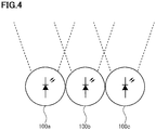
- FIG. 4 is a conceptual diagram showing a configuration example of a vehicular lamp that is configured using the light emitting elements and the driving devices thereof according to the above-described embodiment.
- the illustrated vehicular lamp includes three units 100a, 100b, and 100c.
- Each of the units 100a, 100b, and 100c includes the above-described light emitting element and its driving device (refer to FIG.1 ), and it is possible to irradiate light of each unit independently and to control the outgoing light intensity independently as well. According to such a vehicular lamp, it is possible to control the outgoing light intensity of each unit with high accuracy.
- a vehicular lamp is shown as an application example of the present invention in the above-described embodiment, the application of the present invention is not limited thereto, and may be applied to various lighting apparatus (or light sources) using a light emitting element.
Landscapes
- Circuit Arrangement For Electric Light Sources In General (AREA)
- Lighting Device Outwards From Vehicle And Optical Signal (AREA)
Abstract
Description
- The present invention relates to a lighting control technique for a light emitting element such as an LED.
- Japanese Patent No.
6201700 - In the light sources using LEDs as described above, one of the methods for controlling the intensity of the outgoing light of the LEDs is to perform pulse width modulation to the voltage supplied to the LEDs. In this case, the outgoing light intensity can be controlled by increasing or decreasing the duty ratio of the voltage.
- Here, when controlling the intensity of the outgoing light of the LEDs by performing pulse width modulation, there is a time lag between the time when the voltage is applied to the LEDs and the time when the electric current actually flows to the LEDs. This is due to the parasitic capacitance and parasitic resistance present on the circuit including the LEDs. In many cases, this time lag is as small as several micro seconds (µs).
- However, when the outgoing light intensity of the LEDs is set extremely low, the influence of the lime lag cannot be ignored in some cases. This is because the ON time period (hereinafter referred to as ON time), which is the period during which the voltage is applied, becomes so short that the ratio of the time lag to the ON time becomes high.
- Thus, the actual ON time is likely to become shorter than the originally intended ON time set for obtaining the specified outgoing light intensity, and there is a problem that the outgoing light intensity does not reach the specified value. Such a problem is not limited to a vehicle headlight apparatus but may also occur in a lighting apparatus using a light emitting element such as an LED.
- In a specific aspect, it is an object of the present invention to provide a technique capable of improving the accuracy of the outgoing light intensity from the light emitting element when performing pulse width modulation.
-
- [1] A control device according to one aspect of the present invention is (a) a control device for controlling a light emitting element by performing pulse width modulation including (b) a DC-DC converter for supplying voltage to the light emitting element, (c) a setting unit that sets a control value for the pulse width modulation in the DC-DC converter, (d) a detection unit that detects an actual value of an ON time period which is a period during which electric current flowing through the light emitting element is relatively high, and (e) a correction unit for correcting the control value set by the setting unit so as to reduce the difference between a specified value of the ON time period corresponding to the control value and the actual value of the ON time period detected by the detection unit
- [2] A control method according to one aspect of the present invention is (a) a control method for controlling the light emitting element by performing pulse width modulation including (b) a first step for setting a control value of the pulse width modulation in a DC-DC converter that supplies a voltage to the light emitting element, (c) a second step for detecting an actual value of an ON time period which is a period in which electric current flowing through the light emitting element is relatively high, and (d) a third step for correcting the control value so as to reduce the difference between a specified value of the ON time period corresponding to the control value and the actual value of the ON time period detected by the detecting unit.
- [3] A lighting apparatus according to one aspect of the present invention includes the above-described control device and a light emitting element controlled by the control device.
- According to the above configurations, it is possible to improve the accuracy of the outgoing light intensity of the light emitting element by performing pulse width modulation.
-
FIG.1 is a diagram showing a configuration of a driving device of a light emitting element according to one embodiment. -
FIGS.2A and 2B are conceptual waveform diagrams showing electric current flowing through the light emitting element. -
FIG.3 is a flowchart showing the operation procedure of the control unit. -
FIG.4 is a conceptual diagram showing a configuration example of a vehicular lamp. -
FIG.1 is a diagram showing a configuration of a driving device of a light emitting element according to one embodiment. The driving device (control device) of the light emitting element shown in the figure controls the lighting state of the light emitting element by receiving power from thepower source 1, and is configured to includes a DC-DC converter 2, acontrol unit 3, alight emitting element 4, and a currentdetection resistance element 5. Here,resistance 6 in the circuit represents a parasitic resistance, andcapacitor 7 represents a parasitic capacitance. - The DC-
DC converter 2 is of a switching type and supplies to the light emitting element 4 a pulse width modulated DC voltage with a duty ratio based on a control signal provided from thecontrol unit 3. The light intensity of thelight emitting element 4 can be controlled by the duty ratio of this DC voltage. - The
control unit 3 generates a control signal for setting the duty ratio of the DC voltage in the DC-DC converter 2 and supplies it to the DC-DC converter 2. - The
light emitting element 4 is an LED, for example, and receives voltage from the DC-DC converter 2 and emits light. Here, although only onelight emitting element 4 is shown in the figure, a plurality of light emitting elements may be connected in series, in parallel, or in series and in parallel. - The current
detection resistance element 5 is connected in series with thelight emitting element 4, and is used for thecontrol unit 3 to detect the electric current flowing through thelight emitting element 4. - Here, the "control device for controlling a light emitting element" is configured to include the DC-
DC converter 2, thecontrol unit 3, and the currentdetection resistance element 5. - The above-described
control unit 3 is realized, for example, by executing a predetermined operation program in a microcomputer, and is configured to include a pulse width modulation (hereinafter often abbreviated as PWM) signal generation unit 11 (referred to as "a setting unit"), amemory 12, a PWM output time detection unit 13 (referred to as "a detection unit"), and a correction value setting unit 14 (referred to as "a correction unit"). - The PWM
signal generation unit 11 generates a control signal for setting the duty ratio (the control value) of the DC voltage generated in the DC-DC converter 2 and supplies it to the DC-DC converter 2. Note that a pulse width may be used instead of the duty ratio as the control value. - The
memory 12 is a non-volatile memory, for example, and stores data indicating a specified value of the ON time, which is a period in which electrical current flowing through thelight emitting element 4 is relatively high when voltage is supplied to thelight emitting element 4 based on the duty ratio indicated by the control signal generated by the PWMsignal generating section 11. More specifically, thememory 12 stores a data table indicating the correspondence between each duty ratio and the specified value of the ON time with respect to each duty ratio. The term "specified value" as used herein refers to the length of the ON time period which is specified from the design or theoretical point of view. - The PWM output
time detection unit 13 detects the actual value (the PWM output time) of the ON time, which is a period during which the electrical current flowing through thelight emitting element 4 is relatively high, by measuring the electrical current flowing through the current detectingresistance element 5. - The correction
value setting unit 14 reads out from thememory 12 the specified value (data) of the ON time corresponding to the duty ratio indicated by the control signal generated by the PWMsignal generation unit 11. The correctionvalue setting unit 14 then calculates the difference between the specified value of the ON time and the PWM output time detected by the PWM outputtime detecting unit 13 and sets a correction value for correcting the duty ratio so that the PWM output time becomes equal to or becomes close to the specified value of the ON time. This correction value is provided to the PWMsignal generation unit 11. Thereby, the control signal generated by the PWMsignal generating section 11 is corrected. -
FIGS.2A and 2B are conceptual waveform diagrams showing electric current flowing through the light emitting element. The operation of thecontrol unit 3 will now be described with reference to these waveform diagrams. InFIG.2A , assuming that the specified value of the ON time of the electrical current flowing through thelight emitting element 4 is t1 (refer to the waveform indicated by the dotted line in the figure), delay occurs in the PWM output time t2 which is the actual value of the ON time (refer to the waveform indicated by the solid line in the figure) due to the influence of parasitic capacitance and parasitic resistance. Here, the PWM outputtime detection unit 13 detects the PWM output time t2. Further, the correctionvalue setting unit 14 reads out from thememory 12 the specified value t1 of the ON time and calculates the difference Δt (delta t) between the specified value t1 and the PWM output time t2 detected by the PWM outputtime detection unit 13. Then, the correctionvalue setting unit 14 sets the correction value so that the PWM output time, which is the actual ON time, is increased by the amount of time corresponding to the difference Δt, and provides it to the PWMsignal generation unit 11. The PWMsignal generation unit 11 sets the duty ratio reflecting the correction value. As a result, as shown inFIG.2B , the duty ratio set by the PWMsignal generation unit 11 is corrected so that the PWM output time is increased by the amount of time corresponding to the difference Δt. -
FIG.3 is a flowchart showing the operation procedure of the control unit. The control method performed by the control unit will now be described below with reference to this flowchart. It should be noted that the order of each process shown in the flowchart can be appropriately changed as long as there is no contradiction in the operation procedure, and the order of the process is not limited to the one shown in the flowchart. - The PWM output
time detection unit 13 in thecontrol unit 3 detects the LED current flowing through the current detection resistance element 5 (step S11), and further detects the PWM output time from the waveform of the LED current (step S12). Specifically, the LED current is converted into a voltage by the currentdetecting resistance element 5, and the PWM output time t2 (refer toFIG.2A ) is detected based on the waveform of the voltage. - Next, the correction
value setting unit 14 reads out from thememory 12 the specified value t1 of the ON time corresponding to the duty ratio indicated by the control signal generated by the PWMsignal generation unit 11, and calculates the difference (error amount) between the ON time t1 of this specified value and the PWM output time t2 which is the actual ON time detected by the PWM outputtime detection unit 13. Then, the correctionvalue setting unit 14 determines whether or not the difference is 1% or more of the specified value t1 (step S13). It should be noted that the criterion "1%" is merely an example and can be set to an appropriate value in accordance with the actual situation. - When the error amount is 1% or more (step S13;YES), the correction
value setting unit 14 sets a correction value so that the PWM output time t2 becomes equal to or close to the specified value according to the difference between the specified value t1 and the PWM output time t2, and outputs the correction value to the PWM signal generation unit 11 (step S14). Upon receiving the correction value, the PWMsignal generation unit 11 sets a duty ratio (or a pulse width modulation width) reflecting the correction value, and outputs the control signal indicating the duty ratio (or the pulse width modulation width) to the DC-DC converter 2 (step S15). - On the other hand, when the error is less than 1% (step S13;NO), the correction
value setting unit 14 does not set a correction value (step S16). Here, the process of not setting a correction value also includes setting the correction value to 0. In this case, the PWMsignal generation unit 11 sets a duty ratio (or a pulse width modulation width) which does not include the correction value, and outputs a control signal indicating the duty ratio (or the pulse width modulation width) to the DC-DC converter 2 (step S15). -
FIG. 4 is a conceptual diagram showing a configuration example of a vehicular lamp that is configured using the light emitting elements and the driving devices thereof according to the above-described embodiment. The illustrated vehicular lamp includes threeunits units FIG.1 ), and it is possible to irradiate light of each unit independently and to control the outgoing light intensity independently as well. According to such a vehicular lamp, it is possible to control the outgoing light intensity of each unit with high accuracy. - According to the embodiment as described above, it is possible to improve the accuracy of the outgoing light intensity of the light emitting element by performing pulse width modulation.
- It should be noted that this invention is not limited to the subject matter of the foregoing embodiment, and can be implemented by being variously modified within the scope of the present invention as defined by the appended claims. For example, in the above-described embodiment, for the purpose of making the description easy to understand, a case where the correction of duty ratio is ideally performed has been described. However, in reality, the advantageous effect of the present invention can also be achieved not only in the case where the difference Δt of the ON time is completely corrected but also in a case where the difference Δt of the ON time becomes smaller.
- Further, although a vehicular lamp is shown as an application example of the present invention in the above-described embodiment, the application of the present invention is not limited thereto, and may be applied to various lighting apparatus (or light sources) using a light emitting element.
Claims (5)
- A control device for controlling a light emitting element by performing pulse width modulation comprising:a DC-DC converter for supplying voltage to the light emitting element,a setting unit that sets a control value for the pulse width modulation in the DC-DC converter,a detection unit that detects an actual value of an ON time period which is a period during which the current flowing through the light emitting element is relatively high, anda correction unit for correcting the control value set by the setting unit so as to reduce the difference between a specified value of the ON time period corresponding to the control value and the actual value of the ON time period detected by the detection unit.
- The control device for controlling the light emitting element according to claim 1,
further comprising a memory which stores data indicating the correspondence between the control value and the specified value of the ON time period,
wherein the correction unit corrects the control value by obtaining the specified value of the ON time period from the memory. - The control device for controlling the light emitting element according to claim 1 or 2,
wherein the difference between the specified value of the ON time period and the actual value of the ON time period is generated by a parasitic resistance and/or a parasitic capacitance on a circuit including the light emitting element. - A control method for controlling a light emitting element by performing pulse width modulation comprising:a first step for setting a control value of the pulse width modulation in a DC-DC converter that supplies a voltage to the light emitting element,a second step for detecting an actual value of an ON time period which is a period in which the current flowing through the light emitting element is relatively high, anda third step for correcting the control value so as to reduce the difference between a specified value of the ON time period corresponding to the control value and the actual value of the ON time period detected by the second step.
- A lighting apparatus comprising:the control device for controlling the light emitting element according to any one of claims 1 to 3, anda light emitting element controlled by the control device.
Applications Claiming Priority (1)
| Application Number | Priority Date | Filing Date | Title |
|---|---|---|---|
| JP2018020352A JP7033943B2 (en) | 2018-02-07 | 2018-02-07 | Light emitting element control device, light emitting element control method, lighting device |
Publications (2)
| Publication Number | Publication Date |
|---|---|
| EP3525553A1 true EP3525553A1 (en) | 2019-08-14 |
| EP3525553B1 EP3525553B1 (en) | 2020-08-12 |
Family
ID=65279496
Family Applications (1)
| Application Number | Title | Priority Date | Filing Date |
|---|---|---|---|
| EP19155381.7A Active EP3525553B1 (en) | 2018-02-07 | 2019-02-04 | Control device for light emitting element, control method for light emitting element, lighting apparatus |
Country Status (3)
| Country | Link |
|---|---|
| US (1) | US20190246468A1 (en) |
| EP (1) | EP3525553B1 (en) |
| JP (1) | JP7033943B2 (en) |
Citations (3)
| Publication number | Priority date | Publication date | Assignee | Title |
|---|---|---|---|---|
| JPS621700B2 (en) | 1984-03-06 | 1987-01-14 | Amusetsuku Kk | |
| US8975831B1 (en) * | 2013-11-27 | 2015-03-10 | Linear Technology Corporation | Pre-charging inductor in switching converter while delaying PWM dimming signal to achieve high PWM dimming ratio in LED drivers |
| US20150076999A1 (en) * | 2013-09-16 | 2015-03-19 | Dialog Semiconductor Inc. | Modifying Duty Cycles of PWM Drive Signals to Compensate for LED Driver Mismatches in a Multi-Channel LED System |
Family Cites Families (5)
| Publication number | Priority date | Publication date | Assignee | Title |
|---|---|---|---|---|
| US8362706B1 (en) * | 2008-12-19 | 2013-01-29 | Cypress Semiconductor Corporation | Current compensation scheme for LED current control |
| JP5962434B2 (en) * | 2012-10-25 | 2016-08-03 | 豊田合成株式会社 | Dimming control system |
| US9402289B1 (en) * | 2013-12-19 | 2016-07-26 | Cooledge Lighting, Inc. | Dimming control for illumination systems |
| DE102014202077B4 (en) * | 2014-02-05 | 2026-03-05 | Robert Bosch Gmbh | Digital circuit for generating a pulse-width modulated signal, especially for controlling an analog quantity |
| JP6331539B2 (en) * | 2014-03-19 | 2018-05-30 | カシオ計算機株式会社 | Driving device, light source driving device, light source device, projection device, and driving method |
-
2018
- 2018-02-07 JP JP2018020352A patent/JP7033943B2/en active Active
-
2019
- 2019-02-04 EP EP19155381.7A patent/EP3525553B1/en active Active
- 2019-02-04 US US16/267,140 patent/US20190246468A1/en not_active Abandoned
Patent Citations (3)
| Publication number | Priority date | Publication date | Assignee | Title |
|---|---|---|---|---|
| JPS621700B2 (en) | 1984-03-06 | 1987-01-14 | Amusetsuku Kk | |
| US20150076999A1 (en) * | 2013-09-16 | 2015-03-19 | Dialog Semiconductor Inc. | Modifying Duty Cycles of PWM Drive Signals to Compensate for LED Driver Mismatches in a Multi-Channel LED System |
| US8975831B1 (en) * | 2013-11-27 | 2015-03-10 | Linear Technology Corporation | Pre-charging inductor in switching converter while delaying PWM dimming signal to achieve high PWM dimming ratio in LED drivers |
Also Published As
| Publication number | Publication date |
|---|---|
| EP3525553B1 (en) | 2020-08-12 |
| JP7033943B2 (en) | 2022-03-11 |
| JP2019139890A (en) | 2019-08-22 |
| US20190246468A1 (en) | 2019-08-08 |
Similar Documents
| Publication | Publication Date | Title |
|---|---|---|
| US8339053B2 (en) | LED dimming apparatus | |
| US8736194B2 (en) | LED dimmer circuit | |
| US8970136B2 (en) | Semiconductor light source lighting circuit and vehicular lamp | |
| US8405325B2 (en) | LED lighting power source and LED lighting system | |
| US20090224695A1 (en) | Drive circuit for driving a load with constant current | |
| US10470273B2 (en) | Light emission drive device and vehicle lamp | |
| US8975831B1 (en) | Pre-charging inductor in switching converter while delaying PWM dimming signal to achieve high PWM dimming ratio in LED drivers | |
| US9623791B2 (en) | Lighting device, vehicle illumination device, and vehicle | |
| CN103313468B (en) | The gain of self adaptation bipolar junction transistor detects | |
| CN104041184A (en) | Electrical device and method for compensating the influence of the current of a load, especially an LED unit, and a driver device for a load, especially an LED unit | |
| US12101857B2 (en) | Light source driver circuit, optical measuring device comprising the light source driver circuit, device for checking value documents, and method for operating a light source load by means of the light source driver circuit | |
| US11310890B2 (en) | Vehicle lamp control apparatus | |
| US12543256B2 (en) | Lighting control apparatus, lighting control method, lighting apparatus | |
| EP2515612A1 (en) | Lighting device and illumination apparatus having the same | |
| US11464100B2 (en) | Vehicle headlight system | |
| EP3525553B1 (en) | Control device for light emitting element, control method for light emitting element, lighting apparatus | |
| US10834799B2 (en) | Vehicle lamp control apparatus | |
| JP2016091727A (en) | Vehicular lighting fixture system | |
| JP2014157785A (en) | Drive circuit, and lamp for vehicles | |
| US12336069B2 (en) | Constant-current switch-mode power converters for LED lighting and methods thereof | |
| JP2021002440A (en) | Lighting control device, lighting control method, and vehicular lighting fixture | |
| JP6287429B2 (en) | LED lighting device | |
| US9215766B2 (en) | Drive device for light-emitting element | |
| US10433395B2 (en) | Device for driving the electrical power supply of light sources of an automotive vehicle | |
| US11490486B2 (en) | Method for maintaining luminosity when switching input power in automotive lighting devices |
Legal Events
| Date | Code | Title | Description |
|---|---|---|---|
| PUAI | Public reference made under article 153(3) epc to a published international application that has entered the european phase |
Free format text: ORIGINAL CODE: 0009012 |
|
| STAA | Information on the status of an ep patent application or granted ep patent |
Free format text: STATUS: THE APPLICATION HAS BEEN PUBLISHED |
|
| AK | Designated contracting states |
Kind code of ref document: A1 Designated state(s): AL AT BE BG CH CY CZ DE DK EE ES FI FR GB GR HR HU IE IS IT LI LT LU LV MC MK MT NL NO PL PT RO RS SE SI SK SM TR |
|
| AX | Request for extension of the european patent |
Extension state: BA ME |
|
| STAA | Information on the status of an ep patent application or granted ep patent |
Free format text: STATUS: REQUEST FOR EXAMINATION WAS MADE |
|
| 17P | Request for examination filed |
Effective date: 20191111 |
|
| RBV | Designated contracting states (corrected) |
Designated state(s): AL AT BE BG CH CY CZ DE DK EE ES FI FR GB GR HR HU IE IS IT LI LT LU LV MC MK MT NL NO PL PT RO RS SE SI SK SM TR |
|
| REG | Reference to a national code |
Ref country code: DE Ref legal event code: R079 Ref document number: 602019000430 Country of ref document: DE Free format text: PREVIOUS MAIN CLASS: H05B0033080000 Ipc: H05B0045100000 |
|
| GRAP | Despatch of communication of intention to grant a patent |
Free format text: ORIGINAL CODE: EPIDOSNIGR1 |
|
| STAA | Information on the status of an ep patent application or granted ep patent |
Free format text: STATUS: GRANT OF PATENT IS INTENDED |
|
| RIC1 | Information provided on ipc code assigned before grant |
Ipc: H05B 45/37 20200101ALI20200305BHEP Ipc: H05B 45/10 20200101AFI20200305BHEP |
|
| INTG | Intention to grant announced |
Effective date: 20200320 |
|
| GRAS | Grant fee paid |
Free format text: ORIGINAL CODE: EPIDOSNIGR3 |
|
| GRAA | (expected) grant |
Free format text: ORIGINAL CODE: 0009210 |
|
| STAA | Information on the status of an ep patent application or granted ep patent |
Free format text: STATUS: THE PATENT HAS BEEN GRANTED |
|
| AK | Designated contracting states |
Kind code of ref document: B1 Designated state(s): AL AT BE BG CH CY CZ DE DK EE ES FI FR GB GR HR HU IE IS IT LI LT LU LV MC MK MT NL NO PL PT RO RS SE SI SK SM TR |
|
| REG | Reference to a national code |
Ref country code: CH Ref legal event code: EP |
|
| REG | Reference to a national code |
Ref country code: IE Ref legal event code: FG4D |
|
| REG | Reference to a national code |
Ref country code: DE Ref legal event code: R096 Ref document number: 602019000430 Country of ref document: DE |
|
| REG | Reference to a national code |
Ref country code: AT Ref legal event code: REF Ref document number: 1302873 Country of ref document: AT Kind code of ref document: T Effective date: 20200915 |
|
| REG | Reference to a national code |
Ref country code: DE Ref legal event code: R082 Ref document number: 602019000430 Country of ref document: DE Representative=s name: WAGNER & GEYER PARTNERSCHAFT MBB PATENT- UND R, DE Ref country code: DE Ref legal event code: R081 Ref document number: 602019000430 Country of ref document: DE Owner name: STANLEY ELECTRIC CO., LTD., JP Free format text: FORMER OWNER: STANLEY ELECTRIC CO. LTD., TOKYO, JP |
|
| REG | Reference to a national code |
Ref country code: LT Ref legal event code: MG4D |
|
| REG | Reference to a national code |
Ref country code: NL Ref legal event code: MP Effective date: 20200812 |
|
| PG25 | Lapsed in a contracting state [announced via postgrant information from national office to epo] |
Ref country code: NO Free format text: LAPSE BECAUSE OF FAILURE TO SUBMIT A TRANSLATION OF THE DESCRIPTION OR TO PAY THE FEE WITHIN THE PRESCRIBED TIME-LIMIT Effective date: 20201112 Ref country code: GR Free format text: LAPSE BECAUSE OF FAILURE TO SUBMIT A TRANSLATION OF THE DESCRIPTION OR TO PAY THE FEE WITHIN THE PRESCRIBED TIME-LIMIT Effective date: 20201113 Ref country code: BG Free format text: LAPSE BECAUSE OF FAILURE TO SUBMIT A TRANSLATION OF THE DESCRIPTION OR TO PAY THE FEE WITHIN THE PRESCRIBED TIME-LIMIT Effective date: 20201112 Ref country code: FI Free format text: LAPSE BECAUSE OF FAILURE TO SUBMIT A TRANSLATION OF THE DESCRIPTION OR TO PAY THE FEE WITHIN THE PRESCRIBED TIME-LIMIT Effective date: 20200812 Ref country code: LT Free format text: LAPSE BECAUSE OF FAILURE TO SUBMIT A TRANSLATION OF THE DESCRIPTION OR TO PAY THE FEE WITHIN THE PRESCRIBED TIME-LIMIT Effective date: 20200812 Ref country code: HR Free format text: LAPSE BECAUSE OF FAILURE TO SUBMIT A TRANSLATION OF THE DESCRIPTION OR TO PAY THE FEE WITHIN THE PRESCRIBED TIME-LIMIT Effective date: 20200812 Ref country code: SE Free format text: LAPSE BECAUSE OF FAILURE TO SUBMIT A TRANSLATION OF THE DESCRIPTION OR TO PAY THE FEE WITHIN THE PRESCRIBED TIME-LIMIT Effective date: 20200812 |
|
| REG | Reference to a national code |
Ref country code: AT Ref legal event code: MK05 Ref document number: 1302873 Country of ref document: AT Kind code of ref document: T Effective date: 20200812 |
|
| PG25 | Lapsed in a contracting state [announced via postgrant information from national office to epo] |
Ref country code: LV Free format text: LAPSE BECAUSE OF FAILURE TO SUBMIT A TRANSLATION OF THE DESCRIPTION OR TO PAY THE FEE WITHIN THE PRESCRIBED TIME-LIMIT Effective date: 20200812 Ref country code: PL Free format text: LAPSE BECAUSE OF FAILURE TO SUBMIT A TRANSLATION OF THE DESCRIPTION OR TO PAY THE FEE WITHIN THE PRESCRIBED TIME-LIMIT Effective date: 20200812 Ref country code: RS Free format text: LAPSE BECAUSE OF FAILURE TO SUBMIT A TRANSLATION OF THE DESCRIPTION OR TO PAY THE FEE WITHIN THE PRESCRIBED TIME-LIMIT Effective date: 20200812 Ref country code: NL Free format text: LAPSE BECAUSE OF FAILURE TO SUBMIT A TRANSLATION OF THE DESCRIPTION OR TO PAY THE FEE WITHIN THE PRESCRIBED TIME-LIMIT Effective date: 20200812 Ref country code: IS Free format text: LAPSE BECAUSE OF FAILURE TO SUBMIT A TRANSLATION OF THE DESCRIPTION OR TO PAY THE FEE WITHIN THE PRESCRIBED TIME-LIMIT Effective date: 20201212 |
|
| PG25 | Lapsed in a contracting state [announced via postgrant information from national office to epo] |
Ref country code: SM Free format text: LAPSE BECAUSE OF FAILURE TO SUBMIT A TRANSLATION OF THE DESCRIPTION OR TO PAY THE FEE WITHIN THE PRESCRIBED TIME-LIMIT Effective date: 20200812 Ref country code: EE Free format text: LAPSE BECAUSE OF FAILURE TO SUBMIT A TRANSLATION OF THE DESCRIPTION OR TO PAY THE FEE WITHIN THE PRESCRIBED TIME-LIMIT Effective date: 20200812 Ref country code: RO Free format text: LAPSE BECAUSE OF FAILURE TO SUBMIT A TRANSLATION OF THE DESCRIPTION OR TO PAY THE FEE WITHIN THE PRESCRIBED TIME-LIMIT Effective date: 20200812 Ref country code: DK Free format text: LAPSE BECAUSE OF FAILURE TO SUBMIT A TRANSLATION OF THE DESCRIPTION OR TO PAY THE FEE WITHIN THE PRESCRIBED TIME-LIMIT Effective date: 20200812 Ref country code: CZ Free format text: LAPSE BECAUSE OF FAILURE TO SUBMIT A TRANSLATION OF THE DESCRIPTION OR TO PAY THE FEE WITHIN THE PRESCRIBED TIME-LIMIT Effective date: 20200812 |
|
| REG | Reference to a national code |
Ref country code: DE Ref legal event code: R097 Ref document number: 602019000430 Country of ref document: DE |
|
| PG25 | Lapsed in a contracting state [announced via postgrant information from national office to epo] |
Ref country code: AT Free format text: LAPSE BECAUSE OF FAILURE TO SUBMIT A TRANSLATION OF THE DESCRIPTION OR TO PAY THE FEE WITHIN THE PRESCRIBED TIME-LIMIT Effective date: 20200812 Ref country code: AL Free format text: LAPSE BECAUSE OF FAILURE TO SUBMIT A TRANSLATION OF THE DESCRIPTION OR TO PAY THE FEE WITHIN THE PRESCRIBED TIME-LIMIT Effective date: 20200812 Ref country code: ES Free format text: LAPSE BECAUSE OF FAILURE TO SUBMIT A TRANSLATION OF THE DESCRIPTION OR TO PAY THE FEE WITHIN THE PRESCRIBED TIME-LIMIT Effective date: 20200812 |
|
| PLBE | No opposition filed within time limit |
Free format text: ORIGINAL CODE: 0009261 |
|
| STAA | Information on the status of an ep patent application or granted ep patent |
Free format text: STATUS: NO OPPOSITION FILED WITHIN TIME LIMIT |
|
| PG25 | Lapsed in a contracting state [announced via postgrant information from national office to epo] |
Ref country code: SK Free format text: LAPSE BECAUSE OF FAILURE TO SUBMIT A TRANSLATION OF THE DESCRIPTION OR TO PAY THE FEE WITHIN THE PRESCRIBED TIME-LIMIT Effective date: 20200812 |
|
| 26N | No opposition filed |
Effective date: 20210514 |
|
| PG25 | Lapsed in a contracting state [announced via postgrant information from national office to epo] |
Ref country code: IT Free format text: LAPSE BECAUSE OF FAILURE TO SUBMIT A TRANSLATION OF THE DESCRIPTION OR TO PAY THE FEE WITHIN THE PRESCRIBED TIME-LIMIT Effective date: 20200812 |
|
| PG25 | Lapsed in a contracting state [announced via postgrant information from national office to epo] |
Ref country code: SI Free format text: LAPSE BECAUSE OF FAILURE TO SUBMIT A TRANSLATION OF THE DESCRIPTION OR TO PAY THE FEE WITHIN THE PRESCRIBED TIME-LIMIT Effective date: 20200812 |
|
| PG25 | Lapsed in a contracting state [announced via postgrant information from national office to epo] |
Ref country code: MC Free format text: LAPSE BECAUSE OF FAILURE TO SUBMIT A TRANSLATION OF THE DESCRIPTION OR TO PAY THE FEE WITHIN THE PRESCRIBED TIME-LIMIT Effective date: 20200812 |
|
| REG | Reference to a national code |
Ref country code: BE Ref legal event code: MM Effective date: 20210228 |
|
| PG25 | Lapsed in a contracting state [announced via postgrant information from national office to epo] |
Ref country code: LU Free format text: LAPSE BECAUSE OF NON-PAYMENT OF DUE FEES Effective date: 20210204 |
|
| PG25 | Lapsed in a contracting state [announced via postgrant information from national office to epo] |
Ref country code: IE Free format text: LAPSE BECAUSE OF NON-PAYMENT OF DUE FEES Effective date: 20210204 |
|
| PG25 | Lapsed in a contracting state [announced via postgrant information from national office to epo] |
Ref country code: BE Free format text: LAPSE BECAUSE OF NON-PAYMENT OF DUE FEES Effective date: 20210228 |
|
| REG | Reference to a national code |
Ref country code: CH Ref legal event code: PL |
|
| PG25 | Lapsed in a contracting state [announced via postgrant information from national office to epo] |
Ref country code: LI Free format text: LAPSE BECAUSE OF NON-PAYMENT OF DUE FEES Effective date: 20220228 Ref country code: CH Free format text: LAPSE BECAUSE OF NON-PAYMENT OF DUE FEES Effective date: 20220228 |
|
| PG25 | Lapsed in a contracting state [announced via postgrant information from national office to epo] |
Ref country code: PT Free format text: LAPSE BECAUSE OF FAILURE TO SUBMIT A TRANSLATION OF THE DESCRIPTION OR TO PAY THE FEE WITHIN THE PRESCRIBED TIME-LIMIT Effective date: 20201214 |
|
| PG25 | Lapsed in a contracting state [announced via postgrant information from national office to epo] |
Ref country code: CY Free format text: LAPSE BECAUSE OF FAILURE TO SUBMIT A TRANSLATION OF THE DESCRIPTION OR TO PAY THE FEE WITHIN THE PRESCRIBED TIME-LIMIT Effective date: 20200812 |
|
| PG25 | Lapsed in a contracting state [announced via postgrant information from national office to epo] |
Ref country code: HU Free format text: LAPSE BECAUSE OF FAILURE TO SUBMIT A TRANSLATION OF THE DESCRIPTION OR TO PAY THE FEE WITHIN THE PRESCRIBED TIME-LIMIT; INVALID AB INITIO Effective date: 20190204 |
|
| PG25 | Lapsed in a contracting state [announced via postgrant information from national office to epo] |
Ref country code: MK Free format text: LAPSE BECAUSE OF FAILURE TO SUBMIT A TRANSLATION OF THE DESCRIPTION OR TO PAY THE FEE WITHIN THE PRESCRIBED TIME-LIMIT Effective date: 20200812 |
|
| PGFP | Annual fee paid to national office [announced via postgrant information from national office to epo] |
Ref country code: DE Payment date: 20231228 Year of fee payment: 6 |
|
| PG25 | Lapsed in a contracting state [announced via postgrant information from national office to epo] |
Ref country code: MT Free format text: LAPSE BECAUSE OF FAILURE TO SUBMIT A TRANSLATION OF THE DESCRIPTION OR TO PAY THE FEE WITHIN THE PRESCRIBED TIME-LIMIT Effective date: 20200812 |
|
| REG | Reference to a national code |
Ref country code: DE Ref legal event code: R119 Ref document number: 602019000430 Country of ref document: DE |
|
| PG25 | Lapsed in a contracting state [announced via postgrant information from national office to epo] |
Ref country code: TR Free format text: LAPSE BECAUSE OF FAILURE TO SUBMIT A TRANSLATION OF THE DESCRIPTION OR TO PAY THE FEE WITHIN THE PRESCRIBED TIME-LIMIT Effective date: 20200812 |
|
| PG25 | Lapsed in a contracting state [announced via postgrant information from national office to epo] |
Ref country code: DE Free format text: LAPSE BECAUSE OF NON-PAYMENT OF DUE FEES Effective date: 20250902 |
|
| PGFP | Annual fee paid to national office [announced via postgrant information from national office to epo] |
Ref country code: FR Payment date: 20251231 Year of fee payment: 8 |
|
| PGFP | Annual fee paid to national office [announced via postgrant information from national office to epo] |
Ref country code: GB Payment date: 20260106 Year of fee payment: 8 |