EP3525336A1 - Capacitor unit, and electric compressor - Google Patents
Capacitor unit, and electric compressor Download PDFInfo
- Publication number
- EP3525336A1 EP3525336A1 EP17869973.2A EP17869973A EP3525336A1 EP 3525336 A1 EP3525336 A1 EP 3525336A1 EP 17869973 A EP17869973 A EP 17869973A EP 3525336 A1 EP3525336 A1 EP 3525336A1
- Authority
- EP
- European Patent Office
- Prior art keywords
- harness
- side terminal
- capacitor unit
- board
- power source
- Prior art date
- Legal status (The legal status is an assumption and is not a legal conclusion. Google has not performed a legal analysis and makes no representation as to the accuracy of the status listed.)
- Granted
Links
Images




Classifications
-
- H—ELECTRICITY
- H02—GENERATION; CONVERSION OR DISTRIBUTION OF ELECTRIC POWER
- H02M—APPARATUS FOR CONVERSION BETWEEN AC AND AC, BETWEEN AC AND DC, OR BETWEEN DC AND DC, AND FOR USE WITH MAINS OR SIMILAR POWER SUPPLY SYSTEMS; CONVERSION OF DC OR AC INPUT POWER INTO SURGE OUTPUT POWER; CONTROL OR REGULATION THEREOF
- H02M7/00—Conversion of AC power input into DC power output; Conversion of DC power input into AC power output
- H02M7/003—Constructional details, e.g. physical layout, assembly, wiring or busbar connections
-
- F—MECHANICAL ENGINEERING; LIGHTING; HEATING; WEAPONS; BLASTING
- F04—POSITIVE - DISPLACEMENT MACHINES FOR LIQUIDS; PUMPS FOR LIQUIDS OR ELASTIC FLUIDS
- F04B—POSITIVE-DISPLACEMENT MACHINES FOR LIQUIDS; PUMPS
- F04B35/00—Piston pumps specially adapted for elastic fluids and characterised by the driving means to their working members, or by combination with, or adaptation to, specific driving engines or motors, not otherwise provided for
- F04B35/04—Piston pumps specially adapted for elastic fluids and characterised by the driving means to their working members, or by combination with, or adaptation to, specific driving engines or motors, not otherwise provided for the means being electric
-
- F—MECHANICAL ENGINEERING; LIGHTING; HEATING; WEAPONS; BLASTING
- F25—REFRIGERATION OR COOLING; COMBINED HEATING AND REFRIGERATION SYSTEMS; HEAT PUMP SYSTEMS; MANUFACTURE OR STORAGE OF ICE; LIQUEFACTION SOLIDIFICATION OF GASES
- F25B—REFRIGERATION MACHINES, PLANTS OR SYSTEMS; COMBINED HEATING AND REFRIGERATION SYSTEMS; HEAT PUMP SYSTEMS
- F25B1/00—Compression machines, plants or systems with non-reversible cycle
- F25B1/005—Compression machines, plants or systems with non-reversible cycle of the single unit type
-
- H—ELECTRICITY
- H02—GENERATION; CONVERSION OR DISTRIBUTION OF ELECTRIC POWER
- H02K—DYNAMO-ELECTRIC MACHINES
- H02K11/00—Structural association of dynamo-electric machines with electric components or with devices for shielding, monitoring or protection
- H02K11/0094—Structural association with other electrical or electronic devices
-
- H—ELECTRICITY
- H02—GENERATION; CONVERSION OR DISTRIBUTION OF ELECTRIC POWER
- H02K—DYNAMO-ELECTRIC MACHINES
- H02K11/00—Structural association of dynamo-electric machines with electric components or with devices for shielding, monitoring or protection
- H02K11/30—Structural association with control circuits or drive circuits
- H02K11/33—Drive circuits, e.g. power electronics
-
- H—ELECTRICITY
- H02—GENERATION; CONVERSION OR DISTRIBUTION OF ELECTRIC POWER
- H02K—DYNAMO-ELECTRIC MACHINES
- H02K5/00—Casings; Enclosures; Supports
- H02K5/04—Casings or enclosures characterised by the shape, form or construction thereof
- H02K5/22—Auxiliary parts of casings not covered by groups H02K5/06-H02K5/20, e.g. shaped to form connection boxes or terminal boxes
- H02K5/225—Terminal boxes or connection arrangements
-
- H—ELECTRICITY
- H02—GENERATION; CONVERSION OR DISTRIBUTION OF ELECTRIC POWER
- H02K—DYNAMO-ELECTRIC MACHINES
- H02K5/00—Casings; Enclosures; Supports
- H02K5/24—Casings; Enclosures; Supports specially adapted for suppression or reduction of noise or vibrations
-
- H—ELECTRICITY
- H02—GENERATION; CONVERSION OR DISTRIBUTION OF ELECTRIC POWER
- H02K—DYNAMO-ELECTRIC MACHINES
- H02K7/00—Arrangements for handling mechanical energy structurally associated with dynamo-electric machines, e.g. structural association with mechanical driving motors or auxiliary dynamo-electric machines
- H02K7/14—Structural association with mechanical loads, e.g. with hand-held machine tools or fans
-
- H—ELECTRICITY
- H02—GENERATION; CONVERSION OR DISTRIBUTION OF ELECTRIC POWER
- H02M—APPARATUS FOR CONVERSION BETWEEN AC AND AC, BETWEEN AC AND DC, OR BETWEEN DC AND DC, AND FOR USE WITH MAINS OR SIMILAR POWER SUPPLY SYSTEMS; CONVERSION OF DC OR AC INPUT POWER INTO SURGE OUTPUT POWER; CONTROL OR REGULATION THEREOF
- H02M7/00—Conversion of AC power input into DC power output; Conversion of DC power input into AC power output
- H02M7/42—Conversion of DC power input into AC power output without possibility of reversal
- H02M7/44—Conversion of DC power input into AC power output without possibility of reversal by static converters
- H02M7/48—Conversion of DC power input into AC power output without possibility of reversal by static converters using discharge tubes with control electrode or semiconductor devices with control electrode
-
- F—MECHANICAL ENGINEERING; LIGHTING; HEATING; WEAPONS; BLASTING
- F04—POSITIVE - DISPLACEMENT MACHINES FOR LIQUIDS; PUMPS FOR LIQUIDS OR ELASTIC FLUIDS
- F04C—ROTARY-PISTON, OR OSCILLATING-PISTON, POSITIVE-DISPLACEMENT MACHINES FOR LIQUIDS; ROTARY-PISTON, OR OSCILLATING-PISTON, POSITIVE-DISPLACEMENT PUMPS
- F04C18/00—Rotary-piston pumps specially adapted for elastic fluids
- F04C18/02—Rotary-piston pumps specially adapted for elastic fluids of arcuate-engagement type, i.e. with circular translatory movement of co-operating members, each member having the same number of teeth or tooth-equivalents
- F04C18/0207—Rotary-piston pumps specially adapted for elastic fluids of arcuate-engagement type, i.e. with circular translatory movement of co-operating members, each member having the same number of teeth or tooth-equivalents both members having co-operating elements in spiral form
- F04C18/0215—Rotary-piston pumps specially adapted for elastic fluids of arcuate-engagement type, i.e. with circular translatory movement of co-operating members, each member having the same number of teeth or tooth-equivalents both members having co-operating elements in spiral form where only one member is moving
-
- F—MECHANICAL ENGINEERING; LIGHTING; HEATING; WEAPONS; BLASTING
- F04—POSITIVE - DISPLACEMENT MACHINES FOR LIQUIDS; PUMPS FOR LIQUIDS OR ELASTIC FLUIDS
- F04C—ROTARY-PISTON, OR OSCILLATING-PISTON, POSITIVE-DISPLACEMENT MACHINES FOR LIQUIDS; ROTARY-PISTON, OR OSCILLATING-PISTON, POSITIVE-DISPLACEMENT PUMPS
- F04C2240/00—Components
- F04C2240/80—Other components
- F04C2240/808—Electronic circuits (e.g. inverters) installed inside the machine
-
- H—ELECTRICITY
- H02—GENERATION; CONVERSION OR DISTRIBUTION OF ELECTRIC POWER
- H02K—DYNAMO-ELECTRIC MACHINES
- H02K2211/00—Specific aspects not provided for in the other groups of this subclass relating to measuring or protective devices or electric components
- H02K2211/03—Machines characterised by circuit boards, e.g. pcb
Definitions
- the present invention relates to a capacitor unit and an electric compressor.
- an electric compressor integrally including a compressor that configures the vehicle-mounted air conditioner, a motor that drives the compressor, and a control device that controls the motor.
- a control device of such an electric compressor includes a capacitor unit and a circuit board.
- the circuit board converts DC power smoothed via the capacitor unit into three-phase AC power.
- As the three-phase AC power output from the circuit board is supplied to a stator of the motor, a rotor of the motor rotates and drives a compressor.
- the capacitor unit includes a board side terminal connected to the circuit board side.
- PTL 1 describes a configuration in which a board side terminal is connected to an electrode terminal of a semiconductor module mounted on a circuit board by a screw. Further, the board side terminal is inserted into a through-hole formed on the circuit board and joined to a wiring pattern formed around the through-hole by a solder or the like.
- the present invention provides a capacitor unit and an electric compressor that are capable of suppressing vibration input to the board side terminal and preventing deformation or damage to a connection part between the board side terminal and the circuit board.
- a capacitor unit including: a housing that accommodates a capacitor main body therein; a harness side terminal provided in the housing and connectable to a power source harness for supplying DC power from an outside; and a board side terminal provided in the housing and connectable to a circuit board from which the DC power is output via the capacitor main body, in which the board side terminal extends in a plate shape from a base portion held in the housing toward a distal end portion connected to the circuit board, and has a notch portion recessed inward of the board side terminal in a width direction between the base portion and the distal end portion.
- a first notch portion formed on a first side of the board side terminal in the width direction and a second notch portion formed on a second side of the board side terminal in the width direction may be formed.
- the vibration of the distal end portion with respect to any direction in the width direction of the board side terminal is absorbed by the region in which the first notch portion and the second notch portion are formed.
- the first notch portion and the second notch portion may be formed at an interval in a direction of connecting the base portion and the distal end portion to each other.
- an electric compressor including: the capacitor unit according to any one of the first aspect to the third aspect; a circuit board that is configured to convert the DC power output from the capacitor unit into AC power; a motor rotational ly driven by the AC power output from the circuit board; a compression mechanism driven by the motor; and a casing that accommodates the capacitor unit, the circuit board, the motor, and the compression mechanism.
- the present invention it becomes possible to suppress the vibration input to the board side terminal and prevent deformation or damage to the connection part between the board side terminal and the circuit board.
- FIG. 1 is a schematic view showing a configuration of the electric compressor according to the embodiment of the present invention.
- FIG. 2 is a perspective view showing a circuit board and a capacitor unit provided in the electric compressor.
- FIG. 3 is a perspective view showing the capacitor unit.
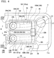
- FIG. 4 is a plan view showing the capacitor unit provided in a casing of the electric compressor.
- FIG. 5 is a side sectional view showing the capacitor unit provided in the casing.
- FIG. 6 is a sectional view showing a connection part between the board side terminal of the capacitor unit and the circuit board.
- an electric compressor 10 of the present embodiment includes a casing 11, a motor 12, a compression mechanism 13, and a driving circuit portion 14.
- the electric compressor 10 configures part of an air conditioner mounted on a vehicle and compresses a refrigerant that circulates in the air conditioner.
- the motor 12, the compression mechanism 13, and the driving circuit portion 14 are accommodated in the casing 11 which forms an outer shell of the electric compressor 10.
- the motor 12 is rotationally driven by AC power output from the driving circuit portion 14.
- the motor 12 has a stator (not shown) and a rotor (not shown).
- the stator generates a magnetic field by the power supplied from a power source 15, such as a battery or a generator of the vehicle.
- the rotor rotates by a magnetic field generated by the stator.
- the compression mechanism 13 is driven by the motor 12.
- the compression mechanism 13 is configured with, for example, a scroll compression mechanism.
- the compression mechanism 13 includes a fixed scroll (not shown) and a turning scroll (not shown).
- the compression mechanism 13 compresses a refrigerant (fluid) as the turning scroll is driven to turn with respect to the fixed scroll by rotation of the rotor (not shown) of the motor 12.
- the driving circuit portion 14 is accommodated inside an opening portion 11a of the casing 11.
- the driving circuit portion 14 includes a capacitor unit 20, the circuit board 30, and a plurality (two in the present embodiment) of power source harnesses 100.
- the capacitor unit 20 removes and smooths a ripple component superimposed on the DC power supplied from the power source 15 and outputs the smoothed DC power to the circuit board 30.
- the circuit board 30 converts the DC power output from the capacitor unit 20 into the AC power and outputs the AC power to the motor 12.
- the circuit board 30 includes a board main body 32, a switching element 33, and a PN terminal forming portion 34.
- the board main body 32 is configured with a plate-like printed board.
- the board main body 32 has a predetermined wiring pattern made of a conductive material, such as copper.
- the board main body 32 is fixed to the casing 11 by a screw or the like (not shown).
- the switching element 33 converts the DC power supplied from the power source 15 on the outside into three-phase AC power.
- the switching element 33 is configured with a plurality of insulated gate bipolar transistors (IGBT) or the like, and is mounted on the board main body 32. Leads 33b of each of the switching elements 33 are inserted into through-holes (not shown) formed in the board main body 32 and are soldered to the wiring pattern of the circuit board 30.
- IGBT insulated gate bipolar transistors
- Each of the switching elements 33 switches between an ON state where a current flows and an OFF state where a current is blocked, based on a driving signal to be input from a control circuit mounted on the circuit board 30.
- the switching elements 33 are each provided two by two corresponding to each of a U phase, a V phase, and a W phase that form a three-phase alternating current.
- the plurality of switching elements 33 supply the three-phase (U phase, V phase, and W phase) AC power to the motor 12 by repeating ON and OFF at a predetermined timing regulated by the driving signal of the control circuit (not shown).
- the switching element 33 is typically an IGBT, but may be a bipolar transistor, a metal-oxide-semiconductor field effect transistor (MOSFET), or the like.
- MOSFET metal-oxide-semiconductor field effect transistor
- the driving circuit portion 14 includes an appropriate electronic component mounted on the circuit board 30.
- the PN terminal forming portion 34 is disposed in an end portion 30a adjacent to the capacitor unit 20 of the circuit board 30.
- the PN terminal forming portion 34 has a pair of a hole portion 35A and a hole portion 35B.
- the board side terminal 24 which is an output terminal of the capacitor unit 20 is connected to the hole portion 35A and the hole portion 35B.
- the capacitor unit 20 includes a capacitor main body 21, a housing 22, a plurality (two in the present embodiment) of harness side terminals 23, a plurality (two in the present embodiment) of board side terminals 24, a plurality (four in the present embodiment) of guide portions 25, a first harness abutting portion 27, and a second harness abutting portion 28.
- the capacitor main body 21 is an electric element that removes and smooths a ripple component superimposed on the DC power supplied from the power source 15.
- the housing 22 is made of a resin made of an insulating material and has a hollow box shape.
- the housing 22 accommodates a capacitor main body 21 on the inside thereof.
- the housing 22 of the present embodiment includes a housing main body 221 and a block portion 222 that protrudes from the housing main body 221.
- the housing main body 221 has a rectangular box shape.
- the housing main body 221 has an upper surface (first surface) 22t which is a surface on which the circuit board 30 is fixed.
- the housing main body 221 has a side surface 22f as a surface orthogonal to the upper surface 22t.
- first end portion 22a the end portion on a side connected to the side surface 22f is referred to as a first end portion 22a.
- second end portion 22b an end portion on a side opposite to the first end portion 22a.
- a direction orthogonal to the upper surface 22t is referred to as an upward-downward direction UD.
- a side that faces the upper surface 22t is referred to as an upper side in the upward-downward direction UD.
- a side opposite to the upper side in the upward-downward direction UD is referred to as a lower side in the upward-downward direction UD.
- a direction orthogonal to the upward-downward direction UD and connecting the first end portion 22a and the second end portion 22b to each other is referred to as a forward-rearward direction (first direction) FR.
- the first end portion 22a side which is a side that faces the side surface 22f is referred to as a front side in the forward-rearward direction FR.
- the second end portion 22b side opposite to the front side in the forward-rearward direction FR is referred to as a rear side in the forward-rearward direction FR.
- a direction orthogonal to the upward-downward direction UD and the forward-rearward direction FR is referred to as a width direction W (second direction).
- the block portion 222 protrudes from the side surface 22f of the housing 22 to the front side in the forward-rearward direction FR.
- the block portion 222 is integrally formed with the housing main body 221.
- the block portion 222 has an L shape in which the inside in the width direction W is recessed when viewed from the upward-downward direction UD.
- a first block portion 222A and a second block portion 222B are provided as the block portion 222.
- the first block portion 222A protrudes from the same position in the width direction W as a first guide portion 25A with respect to the side surface 22f. In the first block portion 222A, the inside in the width direction W is recessed.
- the second block portion 222B protrudes from the same position in the width direction W as a fourth guide portion 25D with respect to the side surface 22f.
- the second block portion 222B is recessed inward in the width direction W so as to face the first block portion 222A.
- the harness side terminal 23 can be connected to the power source harness 100 for supplying the DC power from the outside to the capacitor main body 21.
- the harness side terminal 23 is made of a conductive metal.
- the harness side terminal 23 has an annular shape in which an opening 23h is formed in a center portion.
- the harness side terminal 23 is provided on the upper surface 22t of the housing main body 221.
- the harness side terminal 23 is provided on the upper surface 22t at a position closer to the first end portion 22a side than the center in the forward-rearward direction FR.
- the harness side terminals 23 are disposed at intervals in the width direction W.
- the plurality of harness side terminals 23 in the present embodiment are a first harness side terminal 23A and a second harness side terminal 23B.
- the positions of the first harness side terminal 23A and the second harness side terminal 23B in the forward-rearward direction FR are the same, and are provided at an interval in the width direction W.
- One harness side terminal 23 is provided so as to be sandwiched in the width direction W by the pair of guide portions 25 which will be described later.
- a first power source harness 100A which is one of the harness side terminals 23 for supplying the DC power from the power source 15 to the capacitor main body 21, is connected to the first harness side terminal 23A in the present embodiment.
- a second power source harness 100B which is the power source harness 100 different from the first harness side terminal 23A for supplying the DC power from the power source 15 to the capacitor main body 21, is connected to the second harness side terminal 23B.
- the housing 22 includes screw holes 22h that extend downward from the upper surface 22t of the housing 22 at positions continuous with the openings 23h of the plurality of harness side terminals 23.
- the plurality of guide portions 25 protrude from the upper surface 22t.
- the guide portion 25 extends from the second end portion 22b in the forward-rearward direction FR on the upper surface 22t toward the first end portion 22a.
- the guide portion 25 protrudes in a rectangular plate shape.
- the guide portion 25 of the present embodiment is integrally formed with the housing main body 221 as part of the housing 22.
- the guide portions 25 are provided in pairs on the upper surface 22t so as to be separated from each other in the width direction W.
- the first guide portion 25A and a second guide portion 25B that correspond to the first harness side terminal 23A, and a third guide portion 25C and a fourth guide portion 25D that correspond to the second harness side terminal 23B are respectively formed.
- the first guide portion 25A and the second guide portion 25B are disposed at an interval from each other so as to sandwich the first harness side terminal 23A in the width direction W.
- the third guide portion 25C and the fourth guide portion 25D are disposed at an interval from each other so as to sandwich the second harness side terminal 23B in the width direction W.
- the first harness abutting portion 27 can abut against the power source harness 100 from the inside in the width direction W on the upper surface 22t.
- the first harness abutting portion 27 protrudes from the second end portion 22b side more than the center in the forward-rearward direction FR on the upper surface 22t.
- the first harness abutting portion 27 of the present embodiment is integrally formed with the housing main body 221 as part of the housing 22.
- the first harness abutting portion 27 protrudes in the upward-downward direction UD orthogonal to the upper surface 22t in the center portion in the width direction W in the second end portion 22b of the upper surface 22t.
- the first harness abutting portion 27 protrudes in the center portion in the width direction W in a rectangular cylinder shape having rounded corner portions.
- the first harness abutting portion 27 is formed continuously with the second guide portion 25B and the third guide portion 25C.
- the second harness abutting portion 28 can abut against the power source harness 100 from the lower side in the upward-downward direction UD on the upper surface 22t.
- the second harness abutting portion 28 is provided to be adjacent to both sides of the first harness abutting portion 27 in the width direction W in the second end portion 22b of the housing main body 221.
- the second harness abutting portion 28 of the present embodiment is integrally formed with the housing main body 221 as part of the housing 22.
- the second harness abutting portion 28 has a top surface 28t that protrudes to the upper side in the upward-downward direction UD from the upper surface 22t of the housing 22.
- the second harness abutting portion 28 has a smaller protrusion dimension from the upper surface 22t of the housing 22 than the first harness abutting portion 27.
- the guide portion 25, the first harness abutting portion 27, and the second harness abutting portion 28 are not limited to a case of being integrally formed with the housing 22.
- the guide portion 25, the first harness abutting portion 27, and the second harness abutting portion 28 may be formed by fixing a different member to the housing 22.
- the board side terminal 24 is provided on the side surface 22f of the first end portion 22a of the housing 22.
- the board side terminal 24 can be connected to the circuit board 30 so as to output the DC power via the capacitor main body 21.
- the board side terminal 24 of the present embodiment is formed by a plate-like metal plate made of a conductive metal.
- the board side terminal 24 extends in a plate shape from the base portion 24b held by the housing main body 221 toward the distal end portion 24a connected to the circuit board 30. Specifically, the board side terminal 24 extends in a plate shape from the block portion 222 toward the upper side in the upward-downward direction UD.
- the board side terminal 24 extends parallel to the side surface 22f from the block portion 222 toward the upper surface 22t side.
- the board side terminal 24 is provided such that a thickness direction thereof matches the forward-rearward direction FR orthogonal to the side surface 22f.
- the board side terminal 24 is formed with a notch portion 40 which is recessed inward in the width direction W between the base portion 24b and the distal end portion 24a.
- the distal end portion 24a is a region connected to the circuit board 30, and is a region above the center in the upward-downward direction UD in the board side terminal 24.
- the base portion 24b is a region held by the housing 22 and is a region below the center in the upward-downward direction UD in the board side terminal 24.
- a plurality of notch portions 40 are formed for one board side terminal 24.
- a first notch portion 41 and a second notch portion 42 are formed as the plurality of notch portions 40.
- the first notch portion 41 is formed in the board side terminal 24 so as to be recessed inward (second side) in the width direction W from an outer edge portion 24s on the outside (first side) of the board side terminal 24 in the width direction W.
- the second notch portion 42 is formed in the board side terminal 24 so as to be recessed outward in the width direction W from an inner edge portion 24t on the inside of the board side terminal 24 in the width direction W.
- the first notch portion 41 and the second notch portion 42 are formed at an interval in the upward-downward direction UD which is a direction of connecting the base portion 24b and the distal end portion 24a to each other.
- the first notch portion 41 is formed above the second notch portion 42 in the upward-downward direction UD such that the positions of the second notch portion 42 in the upward-downward direction UD do not overlap each other.
- a curved portion 43 is formed by the first notch portion 41 and the second notch portion 42.
- the curved portion 43 has a partially smaller sectional area orthogonal to the upward-downward direction UD in which the board side terminal 24 extends than the distal end portion 24a and the base portion 24b.
- the curved portion 43 extends in a direction inclined with respect to the upward-downward direction UD.
- the plurality of board side terminals 24 in the present embodiment are a first board side terminal 24A and a second board side terminal 24B.
- the positions of the first board side terminal 24A and the second board side terminal 24B in the forward-rearward direction FR are the same and are provided at an interval in the width direction W.
- the first harness side terminal 23A and the first board side terminal 24A are formed in both end portions of an integrally formed first bus bar 45A.
- the second harness side terminal 23B and the second board side terminal 24B are formed in both end portions of an integrally formed second bus bar 45B.
- the first bus bar 45A and the second bus bar 45B are formed by cutting a plate made of a conductive metal into a predetermined shape by pressing or the like, and bending the plate at a plurality of locations in a longitudinal direction.
- the first bus bar 45A and the second bus bar 45B are buried in the housing 22 so as to expose only the first harness side terminal 23A and the second harness side terminal 23B of both end portions and the first board side terminal 24A and the second board side terminal 24B from the housing 22.
- the capacitor unit 20 as described above is disposed at a position along the end portion 30a of the circuit board 30.
- the capacitor unit 20 is fixed to the casing 11 by a screw (not shown) or the like.
- the capacitor unit 20 is connected to the circuit board 30 via the first board side terminal 24A and the second board side terminal 24B.
- the first board side terminal 24A and the second board side terminal 24B are inserted into the hole portion 35A and the hole portion 35B of the board main body 32.
- the first board side terminal 24A and the second board side terminal 24B are soldered to land portions of the wiring pattern formed around the hole portion 35A and the hole portion 35B by a solder 120 (refer to FIG. 6 ).
- the capacitor unit 20 is connected to the power source 15, such as a battery or a generator of a vehicle via the plurality of power source harnesses 100.
- the plurality of power source harnesses 100 respectively include a harness main body 101 and a terminal 102.
- the harness main body 101 is a flexible linear member.
- the harness main body 101 has a wire (not shown) made of a conductive metal and an insulating coating 101a that covers the wire.
- the terminal 102 is made of a conductive metal and has an annular shape. The terminal 102 is fixed to the distal end (one end portion) of the harness main body 101.
- a proximal end (not shown) (the other end portion opposite to the distal end) is connected to a positive electrode or a negative electrode of the power source 15, such as a battery or a generator.
- the terminals 102 provided at the distal end of the power source harness 100 are connected to the harness side terminal 23 by fastening the bolt 110 to the screw hole 22h in a state of being superimposed on the harness side terminal 23.
- the harness main body 101 is disposed to extend from the first end portion 22a to the second end portion 22b side along the upper surface 22t of the housing 22.
- the power source harness 100 extends while being curved downward from the second end portion 22b of the housing 22 toward the casing 11 positioned on the outside, and is inserted through a harness insertion hole 17 formed below the capacitor unit 20.
- the harness insertion hole 17 is formed offset to one side in the width direction W, that is, the first harness side terminal 23A side in the present embodiment, in the capacitor unit 20.
- the plurality of power source harnesses 100 in the present embodiment are a first power source harness 100A and a second power source harness 100B.
- the terminal 102 of the first power source harness 100A is connected to the first harness side terminal 23A.
- the terminal 102 of the second power source harness 100B is connected to the second harness side terminal 23B.
- the first power source harness 100A is disposed along the harness main body 101 between the first guide portion 25A and the second guide portion 25B.
- the second power source harness 100B is disposed along the harness main body 101 between the third guide portion 25C and the fourth guide portion 25D.
- the first power source harness 100A disposed as described above abuts at least one of the first harness abutting portion 27 and the second harness abutting portion 28 in the second end portion 22b of the housing 22.
- the second power source harness 100B abuts at least one of the first harness abutting portion 27 and the second harness abutting portion 28 in the second end portion 22b of the housing 22.
- the outer side in a curve direction of the harness main body 101 comes into contact with the inner peripheral surface (casing side harness abutting portion) 17f of the harness insertion hole 17.
- the first power source harness 100A comes into contact with at least three locations of the first harness side terminal 23A, the first harness abutting portion 27, and the inner peripheral surface 17f of the harness insertion hole 17.
- the second power source harness 100B comes into contact with at least three locations of the second harness side terminal 23B, at least one of the first harness abutting portion 27 and the second harness abutting portion 28, and the inner peripheral surface 17f of the harness insertion hole 17.
- the curved portion 43 having a shorter length and a smaller sectional area in the width direction W than the distal end portions 24a or the base portions 24b is partially formed in the board side terminal 24 by the notch portion 40.
- the curved portion 43 having a smaller sectional area than the distal end portion 24a and the base portion 24b in the board side terminal 24 is elastically deformed in the width direction W. Therefore, the vibration of the distal end portion 24a in the width direction W with respect to the base portion 24b is absorbed by the curved portion 43.
- a first notch portion 41 and a second notch portion 42 which are recessed in different directions in the width direction W are formed. Therefore, the movement of the distal end portion 24a in any direction in the width direction W is also absorbed by the curved portion 43. As a result, it is possible to further suppress stress concentration in the board side terminal 24 connected to the circuit board 30 by the solder. Accordingly, it is possible to effectively suppress the deformation or damage to the solder (connection part) between the board side terminal 24 and the distal end portion 24a.
- the first notch portion 41 and the second notch portion 42 are formed at an interval in the upward-downward direction UD. Therefore, the curved portion 43 can be formed on the board side terminal 24 so as to be curved in an S shape between the distal end portion 24a and the base portion 24b. Such a shape can be formed at the same time even when the board side terminal 24 is thin.
- the first bus bar 45A and the second bus bar 45B are easily formed at the same time by cutting a plate made of a conductive metal into a predetermined shape by pressing or the like. Therefore, it is not necessary to increase the number of processing steps in order to form the curved portion 43, and it is possible to form the first notch portion 41 and the second notch portion 42 which are efficiently recessed in different directions.
- first guide portion 25A and the second guide portion 25B are formed so as to sandwich the first harness side terminal 23A.
- the terminal 102 of the first power source harness 100A is fixed to the first harness side terminal 23A in the first harness side terminal 23A.
- the harness main body 101 of the first power source harness 100A is disposed to extend from the first end portion 22a toward the second end portion 22b on the upper surface 22t in a state of being sandwiched from the width direction W by the first guide portion 25A and the second guide portion 25B.
- the terminal 102 of the second power source harness 100B is fixed to the second harness side terminal 23B.
- the harness main body 101 of the second power source harness 100B is disposed to extend from the first end portion 22a toward the second end portion 22b on the upper surface 22t along the third guide portion 25C and the fourth guide portion 25D. Therefore, the movement of the harness main body 101 of the first power source harness 100A and the second power source harness 100B in the width direction W is restricted by the guide portion 25. Therefore, excessive vibration of the first power source harness 100A and the second power source harness 100B can be suppressed. Accordingly, it becomes possible to suppress the vibration of the power source harness 100 to be connected to the capacitor unit 20.
- the first harness side terminal 23A is sandwiched by the first guide portion 25A and the second guide portion 25B, and the second harness side terminal 23B is separately sandwiched by the third guide portion 25C and the fourth guide portion 25D. Therefore, the guide portions 25 are disposed on both sides in the width direction W of each of the first power source harness 100A fixed to the first harness side terminal 23A and the second power source harness 100B fixed to the second harness side terminal 23B. Accordingly, it is possible to ensure the insulation distance around each of the first power source harness 100A and the second power source harness 100B.
- first power source harness 100A and the second power source harness 100B come into contact with the first harness abutting portion 27 in the width direction W in the second end portion 22b. Therefore, the movement of the first power source harness 100A and the second power source harness 100B in the width direction W is restricted not only on the first end portion 22a side fixed to the harness side terminal 23 but also on the second end portion 22b side. Accordingly, the vibration of the first power source harness 100A and the second power source harness 100B in the width direction W can be effectively suppressed.
- first power source harness 100A and the second power source harness 100B come into contact with the inner peripheral surface 17f of the harness insertion hole 17 formed in the casing 11 from the upper side in the upward-downward direction UD at a part derived from the capacitor unit 20. Additionally, the first power source harness 100A and the second power source harness 100B come into contact with the second harness abutting portion 28 from the lower side the upward-downward direction UD. Accordingly, the first power source harness 100A and the second power source harness 100B are supported to be sandwiched from the upward-downward direction UD at three points of the first harness side terminal 23A and the second harness side terminal 23B, the second harness abutting portion 28, and the inner peripheral surface 17f of the harness insertion hole 17.
- harness side terminal 23 and the board side terminal 24 are provided on the same side of the housing 22 (the first end portion 22a side). Therefore, the connection work between the board side terminal 24 and the circuit board 30 and the connection work between the harness side terminal 23 and the power source harness 100 can be efficiently performed.
- first guide portion 25A and the second guide portion 25B are provided on both sides of the first harness side terminal 23A, and the third guide portion 25C and the fourth guide portion 25D are provided on both sides of the second harness side terminal 23B, but the present invention is not limited thereto.
- the guide portions 25 may be provided at least on only both outer sides of the upper surface 22t in the width direction W similar to the first guide portion 25A and the fourth guide portion 25D.
- the curved portion 43 is configured by forming the notch portion 40 in the board side terminal 24, the number, arrangement, shape, and the like of the notch portion 40 can be appropriately changed.
- each part of the electric compressor 10 can be appropriately changed.
- the air conditioner for vehicles provided with the electric compressor 10 was shown as an example, the present invention is not limited thereto, and the same configuration can also be applied to a refrigeration system provided with the electric compressor 10.
- the capacitor unit and the electric compressor it becomes possible to suppress vibration input to the board side terminal and prevent deformation or damage to the connection part between the board side terminal and the circuit board.
Landscapes
- Engineering & Computer Science (AREA)
- Power Engineering (AREA)
- Microelectronics & Electronic Packaging (AREA)
- Mechanical Engineering (AREA)
- General Engineering & Computer Science (AREA)
- Physics & Mathematics (AREA)
- Thermal Sciences (AREA)
- Inverter Devices (AREA)
- Coupling Device And Connection With Printed Circuit (AREA)
Abstract
Description
- The present invention relates to a capacitor unit and an electric compressor.
- Priority is claimed on Japanese Patent Application No.
2016-220658, filed on November 11, 2016 - For example, in a vehicle-mounted air conditioner, high space saving properties are required because of the need to accommodate various components in a limited space in a vehicle. Therefore, in recent years, in order to improve the space saving properties, there is provided an electric compressor integrally including a compressor that configures the vehicle-mounted air conditioner, a motor that drives the compressor, and a control device that controls the motor.
- A control device of such an electric compressor includes a capacitor unit and a circuit board. The circuit board converts DC power smoothed via the capacitor unit into three-phase AC power. As the three-phase AC power output from the circuit board is supplied to a stator of the motor, a rotor of the motor rotates and drives a compressor.
- The capacitor unit includes a board side terminal connected to the circuit board side. For example, PTL 1 describes a configuration in which a board side terminal is connected to an electrode terminal of a semiconductor module mounted on a circuit board by a screw. Further, the board side terminal is inserted into a through-hole formed on the circuit board and joined to a wiring pattern formed around the through-hole by a solder or the like.
- [PTL 1] Japanese Unexamined Patent Application, First Publication No.
2007-336761 - However, when the circuit board and the capacitor unit vibrate relative to each other due to the vibration generated during traveling of the vehicle, a stress acts on the board side terminal. It is necessary to reliably prevent deformation or damage of the board side terminal due to the stress.
- The present invention provides a capacitor unit and an electric compressor that are capable of suppressing vibration input to the board side terminal and preventing deformation or damage to a connection part between the board side terminal and the circuit board.
- According to a first aspect of the present invention, there is provided a capacitor unit including: a housing that accommodates a capacitor main body therein; a harness side terminal provided in the housing and connectable to a power source harness for supplying DC power from an outside; and a board side terminal provided in the housing and connectable to a circuit board from which the DC power is output via the capacitor main body, in which the board side terminal extends in a plate shape from a base portion held in the housing toward a distal end portion connected to the circuit board, and has a notch portion recessed inward of the board side terminal in a width direction between the base portion and the distal end portion.
- With the configuration, a region having a section smaller than the distal end portion or the base portion is partially formed in the board side terminal by the notch portion. Therefore, the vibration of the distal end portion in the second direction with respect to the base portion is absorbed by the region in which the notch portion is formed. As a result, it is possible to suppress stress concentration in the distal end portion connected to the circuit board.
- In addition, according to a second aspect of the present invention, in the capacitor unit of the first aspect, a first notch portion formed on a first side of the board side terminal in the width direction and a second notch portion formed on a second side of the board side terminal in the width direction, may be formed.
- In this manner, the vibration of the distal end portion with respect to any direction in the width direction of the board side terminal is absorbed by the region in which the first notch portion and the second notch portion are formed. As a result, it is possible to further suppress stress concentration in the distal end portion connected to the circuit board by a solder. Therefore, the vibration transmitted from the circuit board to the board side terminal can be absorbed, and the deformation or damage to the board side terminal can be effectively suppressed.
- In addition, according to a third aspect of the present invention, in the capacitor unit of the second aspect, the first notch portion and the second notch portion may be formed at an interval in a direction of connecting the base portion and the distal end portion to each other.
- With the configuration, it is possible to form an S-shaped curved region between the distal end portion and the base portion for the board side terminal. Such a shape can be formed at the same time with a thin board side terminal by cutting a plate made of a conductive metal into a predetermined shape by pressing or the like. Therefore, it is not necessary to increase the number of processing steps in order to form a curved region, and it is possible to form the first notch portion and the second notch portion which are efficiently recessed in different directions.
- In addition, according to a fourth aspect of the present invention, there is provided an electric compressor including: the capacitor unit according to any one of the first aspect to the third aspect; a circuit board that is configured to convert the DC power output from the capacitor unit into AC power; a motor rotational ly driven by the AC power output from the circuit board; a compression mechanism driven by the motor; and a casing that accommodates the capacitor unit, the circuit board, the motor, and the compression mechanism.
- According to the present invention, it becomes possible to suppress the vibration input to the board side terminal and prevent deformation or damage to the connection part between the board side terminal and the circuit board.
-
-
FIG. 1 is a schematic view showing a configuration of an electric compressor according to an embodiment of the present invention. -
FIG. 2 is a perspective view showing a circuit board and a capacitor unit provided in the electric compressor. -
FIG. 3 is a perspective view showing the capacitor unit. -
FIG. 4 is a plan view showing the capacitor unit provided in a casing of the electric compressor. -
FIG. 5 is a side sectional view showing the capacitor unit provided in the casing. -
FIG. 6 is a sectional view showing a connection part between the board side terminal of the capacitor unit and the circuit board. - Hereinafter, with reference to attached drawings, embodiments for realizing a capacitor unit and an electric compressor according to the present invention will be described. However, the present invention is not limited to the embodiments.
-
FIG. 1 is a schematic view showing a configuration of the electric compressor according to the embodiment of the present invention.FIG. 2 is a perspective view showing a circuit board and a capacitor unit provided in the electric compressor.FIG. 3 is a perspective view showing the capacitor unit.FIG. 4 is a plan view showing the capacitor unit provided in a casing of the electric compressor.FIG. 5 is a side sectional view showing the capacitor unit provided in the casing.FIG. 6 is a sectional view showing a connection part between the board side terminal of the capacitor unit and the circuit board. - As shown in
FIG. 1 , anelectric compressor 10 of the present embodiment includes acasing 11, amotor 12, acompression mechanism 13, and adriving circuit portion 14. Theelectric compressor 10 configures part of an air conditioner mounted on a vehicle and compresses a refrigerant that circulates in the air conditioner. - The
motor 12, thecompression mechanism 13, and thedriving circuit portion 14 are accommodated in thecasing 11 which forms an outer shell of theelectric compressor 10. - The
motor 12 is rotationally driven by AC power output from thedriving circuit portion 14. Themotor 12 has a stator (not shown) and a rotor (not shown). The stator generates a magnetic field by the power supplied from apower source 15, such as a battery or a generator of the vehicle. The rotor rotates by a magnetic field generated by the stator. - The
compression mechanism 13 is driven by themotor 12. Thecompression mechanism 13 is configured with, for example, a scroll compression mechanism. Thecompression mechanism 13 includes a fixed scroll (not shown) and a turning scroll (not shown). Thecompression mechanism 13 compresses a refrigerant (fluid) as the turning scroll is driven to turn with respect to the fixed scroll by rotation of the rotor (not shown) of themotor 12. - As shown in
FIG. 2 , thedriving circuit portion 14 is accommodated inside anopening portion 11a of thecasing 11. Thedriving circuit portion 14 includes acapacitor unit 20, thecircuit board 30, and a plurality (two in the present embodiment) ofpower source harnesses 100. - The
capacitor unit 20 removes and smooths a ripple component superimposed on the DC power supplied from thepower source 15 and outputs the smoothed DC power to thecircuit board 30. - The
circuit board 30 converts the DC power output from thecapacitor unit 20 into the AC power and outputs the AC power to themotor 12. Thecircuit board 30 includes a boardmain body 32, a switchingelement 33, and a PNterminal forming portion 34. - The board
main body 32 is configured with a plate-like printed board. The boardmain body 32 has a predetermined wiring pattern made of a conductive material, such as copper. The boardmain body 32 is fixed to thecasing 11 by a screw or the like (not shown). - The switching
element 33 converts the DC power supplied from thepower source 15 on the outside into three-phase AC power. The switchingelement 33 is configured with a plurality of insulated gate bipolar transistors (IGBT) or the like, and is mounted on the boardmain body 32.Leads 33b of each of the switchingelements 33 are inserted into through-holes (not shown) formed in the boardmain body 32 and are soldered to the wiring pattern of thecircuit board 30. - Each of the switching
elements 33 switches between an ON state where a current flows and an OFF state where a current is blocked, based on a driving signal to be input from a control circuit mounted on thecircuit board 30. In the present embodiment, the switchingelements 33 are each provided two by two corresponding to each of a U phase, a V phase, and a W phase that form a three-phase alternating current. The plurality of switchingelements 33 supply the three-phase (U phase, V phase, and W phase) AC power to themotor 12 by repeating ON and OFF at a predetermined timing regulated by the driving signal of the control circuit (not shown). - In addition, the switching
element 33 is typically an IGBT, but may be a bipolar transistor, a metal-oxide-semiconductor field effect transistor (MOSFET), or the like. - Further, in addition to the switching
element 33, the drivingcircuit portion 14 includes an appropriate electronic component mounted on thecircuit board 30. - The PN
terminal forming portion 34 is disposed in anend portion 30a adjacent to thecapacitor unit 20 of thecircuit board 30. The PNterminal forming portion 34 has a pair of ahole portion 35A and ahole portion 35B. Theboard side terminal 24 which is an output terminal of thecapacitor unit 20 is connected to thehole portion 35A and thehole portion 35B. By connecting theboard side terminal 24 to the PNterminal forming portion 34, the DC power smoothed by thecapacitor unit 20 is input to thecircuit board 30. - As shown in
FIGS. 3 and4 , thecapacitor unit 20 includes a capacitormain body 21, ahousing 22, a plurality (two in the present embodiment) ofharness side terminals 23, a plurality (two in the present embodiment) ofboard side terminals 24, a plurality (four in the present embodiment) ofguide portions 25, a firstharness abutting portion 27, and a secondharness abutting portion 28. - The capacitor
main body 21 is an electric element that removes and smooths a ripple component superimposed on the DC power supplied from thepower source 15. - The
housing 22 is made of a resin made of an insulating material and has a hollow box shape. Thehousing 22 accommodates a capacitormain body 21 on the inside thereof. Thehousing 22 of the present embodiment includes a housingmain body 221 and ablock portion 222 that protrudes from the housingmain body 221. - The housing
main body 221 has a rectangular box shape. The housingmain body 221 has an upper surface (first surface) 22t which is a surface on which thecircuit board 30 is fixed. The housingmain body 221 has aside surface 22f as a surface orthogonal to theupper surface 22t. In the present embodiment, on theupper surface 22t of the housingmain body 221, the end portion on a side connected to theside surface 22f is referred to as afirst end portion 22a. In the present embodiment, on theupper surface 22t, an end portion on a side opposite to thefirst end portion 22a is referred to as asecond end portion 22b. - In addition, in the present embodiment, a direction orthogonal to the
upper surface 22t is referred to as an upward-downward direction UD. In the upward-downward direction UD, a side that faces theupper surface 22t is referred to as an upper side in the upward-downward direction UD. In addition, a side opposite to the upper side in the upward-downward direction UD is referred to as a lower side in the upward-downward direction UD. Further, a direction orthogonal to the upward-downward direction UD and connecting thefirst end portion 22a and thesecond end portion 22b to each other is referred to as a forward-rearward direction (first direction) FR. In the forward-rearward direction FR, thefirst end portion 22a side which is a side that faces theside surface 22f is referred to as a front side in the forward-rearward direction FR. In addition, thesecond end portion 22b side opposite to the front side in the forward-rearward direction FR is referred to as a rear side in the forward-rearward direction FR. Further, a direction orthogonal to the upward-downward direction UD and the forward-rearward direction FR is referred to as a width direction W (second direction). - The
block portion 222 protrudes from theside surface 22f of thehousing 22 to the front side in the forward-rearward direction FR. Theblock portion 222 is integrally formed with the housingmain body 221. Theblock portion 222 has an L shape in which the inside in the width direction W is recessed when viewed from the upward-downward direction UD. In the present embodiment, afirst block portion 222A and asecond block portion 222B are provided as theblock portion 222. - The
first block portion 222A protrudes from the same position in the width direction W as afirst guide portion 25A with respect to theside surface 22f. In thefirst block portion 222A, the inside in the width direction W is recessed. - The
second block portion 222B protrudes from the same position in the width direction W as afourth guide portion 25D with respect to theside surface 22f. Thesecond block portion 222B is recessed inward in the width direction W so as to face thefirst block portion 222A. - The
harness side terminal 23 can be connected to thepower source harness 100 for supplying the DC power from the outside to the capacitormain body 21. Theharness side terminal 23 is made of a conductive metal. Theharness side terminal 23 has an annular shape in which anopening 23h is formed in a center portion. Theharness side terminal 23 is provided on theupper surface 22t of the housingmain body 221. Theharness side terminal 23 is provided on theupper surface 22t at a position closer to thefirst end portion 22a side than the center in the forward-rearward direction FR. Theharness side terminals 23 are disposed at intervals in the width direction W. - The plurality of
harness side terminals 23 in the present embodiment are a firstharness side terminal 23A and a secondharness side terminal 23B. The positions of the firstharness side terminal 23A and the secondharness side terminal 23B in the forward-rearward direction FR are the same, and are provided at an interval in the width direction W. Oneharness side terminal 23 is provided so as to be sandwiched in the width direction W by the pair ofguide portions 25 which will be described later. - Specifically, a first power source harness 100A, which is one of the
harness side terminals 23 for supplying the DC power from thepower source 15 to the capacitormain body 21, is connected to the firstharness side terminal 23A in the present embodiment. Similarly, a secondpower source harness 100B, which is thepower source harness 100 different from the firstharness side terminal 23A for supplying the DC power from thepower source 15 to the capacitormain body 21, is connected to the secondharness side terminal 23B. - As shown in
FIG. 5 , thehousing 22 includesscrew holes 22h that extend downward from theupper surface 22t of thehousing 22 at positions continuous with theopenings 23h of the plurality ofharness side terminals 23. - As shown in
FIGS. 3 to 5 , the plurality ofguide portions 25 protrude from theupper surface 22t. Theguide portion 25 extends from thesecond end portion 22b in the forward-rearward direction FR on theupper surface 22t toward thefirst end portion 22a. Theguide portion 25 protrudes in a rectangular plate shape. Theguide portion 25 of the present embodiment is integrally formed with the housingmain body 221 as part of thehousing 22. Theguide portions 25 are provided in pairs on theupper surface 22t so as to be separated from each other in the width direction W. In the present embodiment, as the plurality ofguide portions 25, thefirst guide portion 25A and asecond guide portion 25B that correspond to the firstharness side terminal 23A, and athird guide portion 25C and afourth guide portion 25D that correspond to the secondharness side terminal 23B are respectively formed. - The
first guide portion 25A and thesecond guide portion 25B are disposed at an interval from each other so as to sandwich the firstharness side terminal 23A in the width direction W. Thethird guide portion 25C and thefourth guide portion 25D are disposed at an interval from each other so as to sandwich the secondharness side terminal 23B in the width direction W. - The first
harness abutting portion 27 can abut against thepower source harness 100 from the inside in the width direction W on theupper surface 22t. The firstharness abutting portion 27 protrudes from thesecond end portion 22b side more than the center in the forward-rearward direction FR on theupper surface 22t. The firstharness abutting portion 27 of the present embodiment is integrally formed with the housingmain body 221 as part of thehousing 22. The firstharness abutting portion 27 protrudes in the upward-downward direction UD orthogonal to theupper surface 22t in the center portion in the width direction W in thesecond end portion 22b of theupper surface 22t. The firstharness abutting portion 27 protrudes in the center portion in the width direction W in a rectangular cylinder shape having rounded corner portions. The firstharness abutting portion 27 is formed continuously with thesecond guide portion 25B and thethird guide portion 25C. - The second
harness abutting portion 28 can abut against thepower source harness 100 from the lower side in the upward-downward direction UD on theupper surface 22t. The secondharness abutting portion 28 is provided to be adjacent to both sides of the firstharness abutting portion 27 in the width direction W in thesecond end portion 22b of the housingmain body 221. The secondharness abutting portion 28 of the present embodiment is integrally formed with the housingmain body 221 as part of thehousing 22. The secondharness abutting portion 28 has atop surface 28t that protrudes to the upper side in the upward-downward direction UD from theupper surface 22t of thehousing 22. The secondharness abutting portion 28 has a smaller protrusion dimension from theupper surface 22t of thehousing 22 than the firstharness abutting portion 27. - In addition, the
guide portion 25, the firstharness abutting portion 27, and the secondharness abutting portion 28 are not limited to a case of being integrally formed with thehousing 22. For example, theguide portion 25, the firstharness abutting portion 27, and the secondharness abutting portion 28 may be formed by fixing a different member to thehousing 22. - The
board side terminal 24 is provided on theside surface 22f of thefirst end portion 22a of thehousing 22. Theboard side terminal 24 can be connected to thecircuit board 30 so as to output the DC power via the capacitormain body 21. Theboard side terminal 24 of the present embodiment is formed by a plate-like metal plate made of a conductive metal. Theboard side terminal 24 extends in a plate shape from thebase portion 24b held by the housingmain body 221 toward thedistal end portion 24a connected to thecircuit board 30. Specifically, theboard side terminal 24 extends in a plate shape from theblock portion 222 toward the upper side in the upward-downward direction UD. Theboard side terminal 24 extends parallel to theside surface 22f from theblock portion 222 toward theupper surface 22t side. Theboard side terminal 24 is provided such that a thickness direction thereof matches the forward-rearward direction FR orthogonal to theside surface 22f. Theboard side terminal 24 is formed with anotch portion 40 which is recessed inward in the width direction W between thebase portion 24b and thedistal end portion 24a. - As shown in
FIGS. 3 and6 , thedistal end portion 24a is a region connected to thecircuit board 30, and is a region above the center in the upward-downward direction UD in theboard side terminal 24. Thebase portion 24b is a region held by thehousing 22 and is a region below the center in the upward-downward direction UD in theboard side terminal 24. - In the present embodiment, a plurality of
notch portions 40 are formed for oneboard side terminal 24. Specifically, in theboard side terminal 24 of the present embodiment, afirst notch portion 41 and asecond notch portion 42 are formed as the plurality ofnotch portions 40. Thefirst notch portion 41 is formed in theboard side terminal 24 so as to be recessed inward (second side) in the width direction W from anouter edge portion 24s on the outside (first side) of theboard side terminal 24 in the width direction W. Thesecond notch portion 42 is formed in theboard side terminal 24 so as to be recessed outward in the width direction W from aninner edge portion 24t on the inside of theboard side terminal 24 in the width direction W. Thefirst notch portion 41 and thesecond notch portion 42 are formed at an interval in the upward-downward direction UD which is a direction of connecting thebase portion 24b and thedistal end portion 24a to each other. Thefirst notch portion 41 is formed above thesecond notch portion 42 in the upward-downward direction UD such that the positions of thesecond notch portion 42 in the upward-downward direction UD do not overlap each other. - In the
board side terminal 24, acurved portion 43 is formed by thefirst notch portion 41 and thesecond notch portion 42. Thecurved portion 43 has a partially smaller sectional area orthogonal to the upward-downward direction UD in which theboard side terminal 24 extends than thedistal end portion 24a and thebase portion 24b. Thecurved portion 43 extends in a direction inclined with respect to the upward-downward direction UD. - The plurality of
board side terminals 24 in the present embodiment are a firstboard side terminal 24A and a secondboard side terminal 24B. The positions of the firstboard side terminal 24A and the secondboard side terminal 24B in the forward-rearward direction FR are the same and are provided at an interval in the width direction W. - The first
harness side terminal 23A and the firstboard side terminal 24A are formed in both end portions of an integrally formedfirst bus bar 45A. In addition, the secondharness side terminal 23B and the secondboard side terminal 24B are formed in both end portions of an integrally formedsecond bus bar 45B. Thefirst bus bar 45A and thesecond bus bar 45B are formed by cutting a plate made of a conductive metal into a predetermined shape by pressing or the like, and bending the plate at a plurality of locations in a longitudinal direction. Thefirst bus bar 45A and thesecond bus bar 45B are buried in thehousing 22 so as to expose only the firstharness side terminal 23A and the secondharness side terminal 23B of both end portions and the firstboard side terminal 24A and the secondboard side terminal 24B from thehousing 22. - As shown in
FIG. 2 , thecapacitor unit 20 as described above is disposed at a position along theend portion 30a of thecircuit board 30. Thecapacitor unit 20 is fixed to thecasing 11 by a screw (not shown) or the like. Thecapacitor unit 20 is connected to thecircuit board 30 via the firstboard side terminal 24A and the secondboard side terminal 24B. As shown inFIGS. 2 and6 , the firstboard side terminal 24A and the secondboard side terminal 24B are inserted into thehole portion 35A and thehole portion 35B of the boardmain body 32. The firstboard side terminal 24A and the secondboard side terminal 24B are soldered to land portions of the wiring pattern formed around thehole portion 35A and thehole portion 35B by a solder 120 (refer toFIG. 6 ). - As shown in
FIGS. 2 ,4 , and5 , thecapacitor unit 20 is connected to thepower source 15, such as a battery or a generator of a vehicle via the plurality of power source harnesses 100. The plurality of power source harnesses 100 respectively include a harnessmain body 101 and a terminal 102. The harnessmain body 101 is a flexible linear member. The harnessmain body 101 has a wire (not shown) made of a conductive metal and an insulatingcoating 101a that covers the wire. The terminal 102 is made of a conductive metal and has an annular shape. The terminal 102 is fixed to the distal end (one end portion) of the harnessmain body 101. - In the
power source harness 100, a proximal end (not shown) (the other end portion opposite to the distal end) is connected to a positive electrode or a negative electrode of thepower source 15, such as a battery or a generator. Theterminals 102 provided at the distal end of thepower source harness 100 are connected to theharness side terminal 23 by fastening thebolt 110 to thescrew hole 22h in a state of being superimposed on theharness side terminal 23. - By being connected to the
harness side terminal 23 in thefirst end portion 22a of thehousing 22, the harnessmain body 101 is disposed to extend from thefirst end portion 22a to thesecond end portion 22b side along theupper surface 22t of thehousing 22. Thepower source harness 100 extends while being curved downward from thesecond end portion 22b of thehousing 22 toward thecasing 11 positioned on the outside, and is inserted through aharness insertion hole 17 formed below thecapacitor unit 20. Here, as shown inFIG. 4 , theharness insertion hole 17 is formed offset to one side in the width direction W, that is, the firstharness side terminal 23A side in the present embodiment, in thecapacitor unit 20. - The plurality of power source harnesses 100 in the present embodiment are a first
power source harness 100A and a secondpower source harness 100B. Theterminal 102 of the firstpower source harness 100A is connected to the firstharness side terminal 23A. Theterminal 102 of the secondpower source harness 100B is connected to the secondharness side terminal 23B. The firstpower source harness 100A is disposed along the harnessmain body 101 between thefirst guide portion 25A and thesecond guide portion 25B. The secondpower source harness 100B is disposed along the harnessmain body 101 between thethird guide portion 25C and thefourth guide portion 25D. - As shown in
FIGS. 4 and5 , the firstpower source harness 100A disposed as described above abuts at least one of the firstharness abutting portion 27 and the secondharness abutting portion 28 in thesecond end portion 22b of thehousing 22. Similarly, the secondpower source harness 100B abuts at least one of the firstharness abutting portion 27 and the secondharness abutting portion 28 in thesecond end portion 22b of thehousing 22. - Furthermore, in the first power source harness 100A and the second
power source harness 100B, the outer side in a curve direction of the harnessmain body 101 comes into contact with the inner peripheral surface (casing side harness abutting portion) 17f of theharness insertion hole 17. - In this manner, the first
power source harness 100A comes into contact with at least three locations of the firstharness side terminal 23A, the firstharness abutting portion 27, and the innerperipheral surface 17f of theharness insertion hole 17. In addition, the secondpower source harness 100B comes into contact with at least three locations of the secondharness side terminal 23B, at least one of the firstharness abutting portion 27 and the secondharness abutting portion 28, and the innerperipheral surface 17f of theharness insertion hole 17. - According to the
capacitor unit 20 and theelectric compressor 10 described above, thecurved portion 43 having a shorter length and a smaller sectional area in the width direction W than thedistal end portions 24a or thebase portions 24b is partially formed in theboard side terminal 24 by thenotch portion 40. Here, when thecapacitor unit 20 and thecircuit board 30 are relatively displaced due to the vibration input from the outside, thecurved portion 43 having a smaller sectional area than thedistal end portion 24a and thebase portion 24b in theboard side terminal 24 is elastically deformed in the width direction W. Therefore, the vibration of thedistal end portion 24a in the width direction W with respect to thebase portion 24b is absorbed by thecurved portion 43. As a result, it is possible to further suppress stress concentration in thedistal end portion 24a connected to thecircuit board 30 by the solder. Therefore, the vibration transmitted from thecircuit board 30 to theboard side terminal 24 can be absorbed by thecurved portion 43, and the deformation or damage to the solder (connection part) between theboard side terminal 24 and thedistal end portion 24a can be suppressed. - Further, a
first notch portion 41 and asecond notch portion 42 which are recessed in different directions in the width direction W are formed. Therefore, the movement of thedistal end portion 24a in any direction in the width direction W is also absorbed by thecurved portion 43. As a result, it is possible to further suppress stress concentration in theboard side terminal 24 connected to thecircuit board 30 by the solder. Accordingly, it is possible to effectively suppress the deformation or damage to the solder (connection part) between theboard side terminal 24 and thedistal end portion 24a. - In addition, the
first notch portion 41 and thesecond notch portion 42 are formed at an interval in the upward-downward direction UD. Therefore, thecurved portion 43 can be formed on theboard side terminal 24 so as to be curved in an S shape between thedistal end portion 24a and thebase portion 24b. Such a shape can be formed at the same time even when theboard side terminal 24 is thin. Specifically, when forming thefirst bus bar 45A and thesecond bus bar 45B, thefirst bus bar 45A and thesecond bus bar 45B are easily formed at the same time by cutting a plate made of a conductive metal into a predetermined shape by pressing or the like. Therefore, it is not necessary to increase the number of processing steps in order to form thecurved portion 43, and it is possible to form thefirst notch portion 41 and thesecond notch portion 42 which are efficiently recessed in different directions. - In addition, the
first guide portion 25A and thesecond guide portion 25B are formed so as to sandwich the firstharness side terminal 23A. Theterminal 102 of the firstpower source harness 100A is fixed to the firstharness side terminal 23A in the firstharness side terminal 23A. Accordingly, the harnessmain body 101 of the firstpower source harness 100A is disposed to extend from thefirst end portion 22a toward thesecond end portion 22b on theupper surface 22t in a state of being sandwiched from the width direction W by thefirst guide portion 25A and thesecond guide portion 25B. Similarly, theterminal 102 of the secondpower source harness 100B is fixed to the secondharness side terminal 23B. Accordingly, the harnessmain body 101 of the secondpower source harness 100B is disposed to extend from thefirst end portion 22a toward thesecond end portion 22b on theupper surface 22t along thethird guide portion 25C and thefourth guide portion 25D. Therefore, the movement of the harnessmain body 101 of the first power source harness 100A and the secondpower source harness 100B in the width direction W is restricted by theguide portion 25. Therefore, excessive vibration of the first power source harness 100A and the secondpower source harness 100B can be suppressed. Accordingly, it becomes possible to suppress the vibration of thepower source harness 100 to be connected to thecapacitor unit 20. - Furthermore, the first
harness side terminal 23A is sandwiched by thefirst guide portion 25A and thesecond guide portion 25B, and the secondharness side terminal 23B is separately sandwiched by thethird guide portion 25C and thefourth guide portion 25D. Therefore, theguide portions 25 are disposed on both sides in the width direction W of each of the firstpower source harness 100A fixed to the firstharness side terminal 23A and the secondpower source harness 100B fixed to the secondharness side terminal 23B. Accordingly, it is possible to ensure the insulation distance around each of the first power source harness 100A and the secondpower source harness 100B. - In addition, the first power source harness 100A and the second
power source harness 100B come into contact with the firstharness abutting portion 27 in the width direction W in thesecond end portion 22b. Therefore, the movement of the first power source harness 100A and the secondpower source harness 100B in the width direction W is restricted not only on thefirst end portion 22a side fixed to theharness side terminal 23 but also on thesecond end portion 22b side. Accordingly, the vibration of the first power source harness 100A and the secondpower source harness 100B in the width direction W can be effectively suppressed. - Furthermore, the first power source harness 100A and the second
power source harness 100B come into contact with the innerperipheral surface 17f of theharness insertion hole 17 formed in thecasing 11 from the upper side in the upward-downward direction UD at a part derived from thecapacitor unit 20. Additionally, the first power source harness 100A and the secondpower source harness 100B come into contact with the secondharness abutting portion 28 from the lower side the upward-downward direction UD. Accordingly, the first power source harness 100A and the secondpower source harness 100B are supported to be sandwiched from the upward-downward direction UD at three points of the firstharness side terminal 23A and the secondharness side terminal 23B, the secondharness abutting portion 28, and the innerperipheral surface 17f of theharness insertion hole 17. As a result, the movement of the firstharness side terminal 23A and the secondharness side terminal 23B in the upward-downward direction UD is restricted. Accordingly, the vibration of the first power source harness 100A and the secondpower source harness 100B in the upward-downward direction UD can be effectively suppressed. - In addition, the
harness side terminal 23 and theboard side terminal 24 are provided on the same side of the housing 22 (thefirst end portion 22a side). Therefore, the connection work between theboard side terminal 24 and thecircuit board 30 and the connection work between theharness side terminal 23 and thepower source harness 100 can be efficiently performed. - Above, although the embodiments of the present invention have been described in detail with reference to the drawings, the respective configurations and combinations thereof in the respective embodiments are merely examples, and additions, omissions, substitutions, and other changes of configurations are possible within the scope that does not depart from the gist of the present invention. In addition, the present invention is not limited by the embodiments, but is limited only by the claims.
- For example, the
first guide portion 25A and thesecond guide portion 25B are provided on both sides of the firstharness side terminal 23A, and thethird guide portion 25C and thefourth guide portion 25D are provided on both sides of the secondharness side terminal 23B, but the present invention is not limited thereto. Theguide portions 25 may be provided at least on only both outer sides of theupper surface 22t in the width direction W similar to thefirst guide portion 25A and thefourth guide portion 25D. - In addition, although the
curved portion 43 is configured by forming thenotch portion 40 in theboard side terminal 24, the number, arrangement, shape, and the like of thenotch portion 40 can be appropriately changed. - In addition, the configuration of each part of the
electric compressor 10 can be appropriately changed. Furthermore, although the air conditioner for vehicles provided with theelectric compressor 10 was shown as an example, the present invention is not limited thereto, and the same configuration can also be applied to a refrigeration system provided with theelectric compressor 10. - According to the capacitor unit and the electric compressor, it becomes possible to suppress vibration input to the board side terminal and prevent deformation or damage to the connection part between the board side terminal and the circuit board.
-
- 10 Electric compressor
- 11 Casing
- 11a Opening portion
- 12 motor
- 13 Compression mechanism
- 14 Driving circuit portion
- 15 Power source
- 17 Harness insertion hole
- 17f Inner peripheral surface (casing side harness abutting portion)
- 20 Capacitor unit
- 21 Capacitor main body
- 22 Housing
- 221 Housing main body
- 222 Block portion
- 222A First block portion
- 222B Second block portion
- 22a First end portion
- 22b Second end portion
- 22f Side surface
- 22h Screw hole
- 22t Upper surface (first surface)
- 23 Harness side terminal
- 23A First harness side terminal
- 23B Second harness side terminal
- 23h Opening
- 24 Board side terminal
- 24A First board side terminal
- 24B Second board side terminal
- 24a Distal end portion
- 24b Base portion
- 24s Outer edge portion
- 24t Inner edge portion
- 25 Guide portion
- 25A First guide portion
- 25B Second guide portion
- 25C Third guide portion
- 25D Fourth guide portion
- 27 First harness abutting portion
- 28 Second harness abutting portion
- 28t Top surface
- 30 Circuit board
- 30a End portion
- 32 Board main body
- 33 Switching element
- 34 PN terminal forming portion
- 35 Electronic component
- 35A, 35B Hole portion
- 40 Notch portion
- 41 First notch portion
- 42 Second notch portion
- 43 Curved portion
- 45A First bus bar
- 45B Second bus bar
- 100 Power source harness
- 100A First power source harness
- 100B Second power source harness
- 101 Harness main body
- 101a Insulating coating
- 102 Terminal
- 110 Bolt
- 120 Solder
- FR Forward-rearward direction (first direction)
- W Width direction (Second direction)
- UD Upward-downward direction
Claims (4)
- A capacitor unit comprising:a housing that accommodates a capacitor main body therein;a harness side terminal provided in the housing and connectable to a power source harness for supplying DC power from an outside; anda board side terminal provided in the housing and connectable to a circuit board from which the DC power is output via the capacitor main body,wherein the board side terminalextends in a plate shape from a base portion held in the housing toward a distal end portion connected to the circuit board, andhas a notch portion recessed inward of the board side terminal in a width direction between the base portion and the distal end portion.
- The capacitor unit according to claim 1,
wherein a first notch portion formed on a first side of the board side terminal in the width direction and a second notch portion formed on a second side of the board side terminal in the width direction, are formed. - The capacitor unit according to claim 2,
wherein the first notch portion and the second notch portion are formed at an interval in a direction of connecting the base portion and the distal end portion to each other. - An electric compressor comprising:the capacitor unit according to any one of claims 1 to 3;the circuit board that is configured to convert the DC power output from the capacitor unit into AC power;a motor rotationally driven by the AC power output from the circuit board;a compression mechanism driven by the motor; anda casing that accommodates the capacitor unit, the circuit board, the motor, and the compression mechanism.
Applications Claiming Priority (2)
| Application Number | Priority Date | Filing Date | Title |
|---|---|---|---|
| JP2016220658A JP6723142B2 (en) | 2016-11-11 | 2016-11-11 | Capacitor unit, electric compressor |
| PCT/JP2017/039561 WO2018088304A1 (en) | 2016-11-11 | 2017-11-01 | Capacitor unit, and electric compressor |
Publications (3)
| Publication Number | Publication Date |
|---|---|
| EP3525336A1 true EP3525336A1 (en) | 2019-08-14 |
| EP3525336A4 EP3525336A4 (en) | 2019-09-11 |
| EP3525336B1 EP3525336B1 (en) | 2021-08-11 |
Family
ID=62109388
Family Applications (1)
| Application Number | Title | Priority Date | Filing Date |
|---|---|---|---|
| EP17869973.2A Active EP3525336B1 (en) | 2016-11-11 | 2017-11-01 | Capacitor unit, and electric compressor |
Country Status (5)
| Country | Link |
|---|---|
| US (1) | US11509186B2 (en) |
| EP (1) | EP3525336B1 (en) |
| JP (1) | JP6723142B2 (en) |
| CN (1) | CN110073587B (en) |
| WO (1) | WO2018088304A1 (en) |
Cited By (1)
| Publication number | Priority date | Publication date | Assignee | Title |
|---|---|---|---|---|
| EP3806296A1 (en) * | 2019-10-11 | 2021-04-14 | Jtekt Corporation | Substrate connecting structure |
Families Citing this family (4)
| Publication number | Priority date | Publication date | Assignee | Title |
|---|---|---|---|---|
| CN111326370A (en) * | 2020-02-29 | 2020-06-23 | 布鲁斯凯技术公司 | Relay control system |
| CN112152366A (en) * | 2020-09-07 | 2020-12-29 | 凯博易控车辆科技(苏州)股份有限公司 | Prevent condensation motor |
| JP2024146243A (en) * | 2023-03-31 | 2024-10-15 | 株式会社豊田自動織機 | Electric Compressor |
| JP2025075216A (en) * | 2023-10-31 | 2025-05-15 | マツダ株式会社 | Power Conversion Equipment |
Family Cites Families (20)
| Publication number | Priority date | Publication date | Assignee | Title |
|---|---|---|---|---|
| GB968587A (en) * | 1960-08-16 | 1964-09-02 | Smith & Sons Ltd S | Improvements in or relating to cam actuated electric switches |
| JP2001211661A (en) * | 2000-01-21 | 2001-08-03 | Mitsubishi Electric Corp | Inverter gate power supply for vehicle |
| JP4026044B2 (en) * | 2000-05-09 | 2007-12-26 | 株式会社デンソー | Board connection member |
| SE525572C2 (en) | 2002-12-23 | 2005-03-15 | Danaher Motion Stockholm Ab | Inverter type motor drive |
| JP2005064358A (en) * | 2003-08-19 | 2005-03-10 | Asahi Keiki Kk | Power supply unit and manufacturing method thereof |
| JP4859443B2 (en) * | 2005-11-17 | 2012-01-25 | 日立オートモティブシステムズ株式会社 | Power converter |
| JP2007250700A (en) * | 2006-03-15 | 2007-09-27 | Hitachi Appliances Inc | Semiconductor device |
| JP2007336761A (en) | 2006-06-19 | 2007-12-27 | Hitachi Ltd | Power converter |
| JP4859939B2 (en) * | 2009-02-19 | 2012-01-25 | 日立オートモティブシステムズ株式会社 | Power converter |
| JP5740986B2 (en) * | 2010-03-17 | 2015-07-01 | 株式会社安川電機 | Power converter |
| JP5422468B2 (en) * | 2010-04-01 | 2014-02-19 | 日立オートモティブシステムズ株式会社 | Power converter |
| JP5766431B2 (en) * | 2010-11-30 | 2015-08-19 | 三菱重工業株式会社 | Electric compressor |
| FR2985597B1 (en) * | 2012-01-05 | 2014-10-24 | Valeo Equip Electr Moteur | CAPACITY ASSEMBLY DEVICE FOR ELECTRONIC CONVERTER |
| JP5749192B2 (en) | 2012-02-13 | 2015-07-15 | 株式会社東芝 | Vehicle drive control device |
| JP6375106B2 (en) * | 2013-09-27 | 2018-08-15 | 三菱重工サーマルシステムズ株式会社 | Circuit assembly having vibration-proof fixing structure for circuit parts, and electric compressor for vehicle |
| JP2017028747A (en) * | 2013-12-05 | 2017-02-02 | 日立オートモティブシステムズ株式会社 | Power converter |
| JP6125985B2 (en) * | 2013-12-12 | 2017-05-10 | 三菱自動車工業株式会社 | Bus bar |
| JP2015126674A (en) * | 2013-12-27 | 2015-07-06 | トヨタ自動車株式会社 | Electric power conversion system |
| JP6294195B2 (en) * | 2014-09-09 | 2018-03-14 | 日立オートモティブシステムズ株式会社 | Power converter |
| JP6580376B2 (en) | 2015-06-04 | 2019-09-25 | タキゲン製造株式会社 | Non-oscillating case for cell / tissue fragment transportation |
-
2016
- 2016-11-11 JP JP2016220658A patent/JP6723142B2/en active Active
-
2017
- 2017-11-01 WO PCT/JP2017/039561 patent/WO2018088304A1/en not_active Ceased
- 2017-11-01 EP EP17869973.2A patent/EP3525336B1/en active Active
- 2017-11-01 US US16/348,384 patent/US11509186B2/en active Active
- 2017-11-01 CN CN201780069501.7A patent/CN110073587B/en active Active
Cited By (2)
| Publication number | Priority date | Publication date | Assignee | Title |
|---|---|---|---|---|
| EP3806296A1 (en) * | 2019-10-11 | 2021-04-14 | Jtekt Corporation | Substrate connecting structure |
| US11309643B2 (en) | 2019-10-11 | 2022-04-19 | Jtekt Corporation | Substrate connecting structure |
Also Published As
| Publication number | Publication date |
|---|---|
| WO2018088304A1 (en) | 2018-05-17 |
| JP2018078771A (en) | 2018-05-17 |
| EP3525336A4 (en) | 2019-09-11 |
| JP6723142B2 (en) | 2020-07-15 |
| EP3525336B1 (en) | 2021-08-11 |
| CN110073587B (en) | 2022-01-11 |
| CN110073587A (en) | 2019-07-30 |
| US20200195086A1 (en) | 2020-06-18 |
| US11509186B2 (en) | 2022-11-22 |
Similar Documents
| Publication | Publication Date | Title |
|---|---|---|
| US11223254B2 (en) | Capacitor unit, and electric compressor | |
| US11509186B2 (en) | Capacitor unit, and electric compressor | |
| US8953335B2 (en) | Semiconductor control device | |
| US10479398B2 (en) | Integrated electric power steering apparatus and manufacturing method therefor | |
| JP2017172509A (en) | Inverter integrated type electric compressor | |
| US9788441B2 (en) | Switching device | |
| WO2014050276A1 (en) | Power conversion apparatus | |
| WO2017073258A1 (en) | Power storage unit | |
| US11632013B2 (en) | Control device and motor device that ensure heat dissipation while reducing the size of the motor device | |
| CN111108677B (en) | semiconductor module unit | |
| US11585332B2 (en) | Electric compressor | |
| US20130265811A1 (en) | Power conversion apparatus having cylindrical casing integrated with connectors | |
| KR101701553B1 (en) | Invertor module for electric compressor | |
| EP2667453A1 (en) | Inter-substrate connection terminal, and inverter and electric compressor using same | |
| US11634170B2 (en) | Electric power-steering control device and electronic unit | |
| JP2006024746A (en) | Electronic circuit equipment | |
| CN118870705A (en) | Power conversion device and motor unit | |
| JP2020077520A (en) | Connection structure, manufacturing method thereof, and inverter device |
Legal Events
| Date | Code | Title | Description |
|---|---|---|---|
| STAA | Information on the status of an ep patent application or granted ep patent |
Free format text: STATUS: THE INTERNATIONAL PUBLICATION HAS BEEN MADE |
|
| PUAI | Public reference made under article 153(3) epc to a published international application that has entered the european phase |
Free format text: ORIGINAL CODE: 0009012 |
|
| STAA | Information on the status of an ep patent application or granted ep patent |
Free format text: STATUS: REQUEST FOR EXAMINATION WAS MADE |
|
| 17P | Request for examination filed |
Effective date: 20190509 |
|
| AK | Designated contracting states |
Kind code of ref document: A1 Designated state(s): AL AT BE BG CH CY CZ DE DK EE ES FI FR GB GR HR HU IE IS IT LI LT LU LV MC MK MT NL NO PL PT RO RS SE SI SK SM TR |
|
| AX | Request for extension of the european patent |
Extension state: BA ME |
|
| A4 | Supplementary search report drawn up and despatched |
Effective date: 20190814 |
|
| RIC1 | Information provided on ipc code assigned before grant |
Ipc: F04B 39/00 20060101ALI20190808BHEP Ipc: H02M 7/48 20070101AFI20190808BHEP Ipc: H02K 5/22 20060101ALI20190808BHEP Ipc: H02K 11/33 20160101ALI20190808BHEP Ipc: H01R 13/56 20060101ALI20190808BHEP Ipc: H02M 7/00 20060101ALI20190808BHEP |
|
| DAV | Request for validation of the european patent (deleted) | ||
| DAX | Request for extension of the european patent (deleted) | ||
| STAA | Information on the status of an ep patent application or granted ep patent |
Free format text: STATUS: EXAMINATION IS IN PROGRESS |
|
| 17Q | First examination report despatched |
Effective date: 20200506 |
|
| GRAP | Despatch of communication of intention to grant a patent |
Free format text: ORIGINAL CODE: EPIDOSNIGR1 |
|
| STAA | Information on the status of an ep patent application or granted ep patent |
Free format text: STATUS: GRANT OF PATENT IS INTENDED |
|
| INTG | Intention to grant announced |
Effective date: 20210316 |
|
| GRAS | Grant fee paid |
Free format text: ORIGINAL CODE: EPIDOSNIGR3 |
|
| GRAA | (expected) grant |
Free format text: ORIGINAL CODE: 0009210 |
|
| STAA | Information on the status of an ep patent application or granted ep patent |
Free format text: STATUS: THE PATENT HAS BEEN GRANTED |
|
| AK | Designated contracting states |
Kind code of ref document: B1 Designated state(s): AL AT BE BG CH CY CZ DE DK EE ES FI FR GB GR HR HU IE IS IT LI LT LU LV MC MK MT NL NO PL PT RO RS SE SI SK SM TR |
|
| REG | Reference to a national code |
Ref country code: CH Ref legal event code: EP |
|
| REG | Reference to a national code |
Ref country code: DE Ref legal event code: R096 Ref document number: 602017044034 Country of ref document: DE |
|
| REG | Reference to a national code |
Ref country code: IE Ref legal event code: FG4D Ref country code: AT Ref legal event code: REF Ref document number: 1420419 Country of ref document: AT Kind code of ref document: T Effective date: 20210915 |
|
| REG | Reference to a national code |
Ref country code: LT Ref legal event code: MG9D |
|
| REG | Reference to a national code |
Ref country code: NL Ref legal event code: MP Effective date: 20210811 |
|
| REG | Reference to a national code |
Ref country code: AT Ref legal event code: MK05 Ref document number: 1420419 Country of ref document: AT Kind code of ref document: T Effective date: 20210811 |
|
| PG25 | Lapsed in a contracting state [announced via postgrant information from national office to epo] |
Ref country code: SE Free format text: LAPSE BECAUSE OF FAILURE TO SUBMIT A TRANSLATION OF THE DESCRIPTION OR TO PAY THE FEE WITHIN THE PRESCRIBED TIME-LIMIT Effective date: 20210811 Ref country code: RS Free format text: LAPSE BECAUSE OF FAILURE TO SUBMIT A TRANSLATION OF THE DESCRIPTION OR TO PAY THE FEE WITHIN THE PRESCRIBED TIME-LIMIT Effective date: 20210811 Ref country code: FI Free format text: LAPSE BECAUSE OF FAILURE TO SUBMIT A TRANSLATION OF THE DESCRIPTION OR TO PAY THE FEE WITHIN THE PRESCRIBED TIME-LIMIT Effective date: 20210811 Ref country code: ES Free format text: LAPSE BECAUSE OF FAILURE TO SUBMIT A TRANSLATION OF THE DESCRIPTION OR TO PAY THE FEE WITHIN THE PRESCRIBED TIME-LIMIT Effective date: 20210811 Ref country code: HR Free format text: LAPSE BECAUSE OF FAILURE TO SUBMIT A TRANSLATION OF THE DESCRIPTION OR TO PAY THE FEE WITHIN THE PRESCRIBED TIME-LIMIT Effective date: 20210811 Ref country code: BG Free format text: LAPSE BECAUSE OF FAILURE TO SUBMIT A TRANSLATION OF THE DESCRIPTION OR TO PAY THE FEE WITHIN THE PRESCRIBED TIME-LIMIT Effective date: 20211111 Ref country code: AT Free format text: LAPSE BECAUSE OF FAILURE TO SUBMIT A TRANSLATION OF THE DESCRIPTION OR TO PAY THE FEE WITHIN THE PRESCRIBED TIME-LIMIT Effective date: 20210811 Ref country code: LT Free format text: LAPSE BECAUSE OF FAILURE TO SUBMIT A TRANSLATION OF THE DESCRIPTION OR TO PAY THE FEE WITHIN THE PRESCRIBED TIME-LIMIT Effective date: 20210811 Ref country code: NO Free format text: LAPSE BECAUSE OF FAILURE TO SUBMIT A TRANSLATION OF THE DESCRIPTION OR TO PAY THE FEE WITHIN THE PRESCRIBED TIME-LIMIT Effective date: 20211111 Ref country code: PT Free format text: LAPSE BECAUSE OF FAILURE TO SUBMIT A TRANSLATION OF THE DESCRIPTION OR TO PAY THE FEE WITHIN THE PRESCRIBED TIME-LIMIT Effective date: 20211213 |
|
| PG25 | Lapsed in a contracting state [announced via postgrant information from national office to epo] |
Ref country code: PL Free format text: LAPSE BECAUSE OF FAILURE TO SUBMIT A TRANSLATION OF THE DESCRIPTION OR TO PAY THE FEE WITHIN THE PRESCRIBED TIME-LIMIT Effective date: 20210811 Ref country code: LV Free format text: LAPSE BECAUSE OF FAILURE TO SUBMIT A TRANSLATION OF THE DESCRIPTION OR TO PAY THE FEE WITHIN THE PRESCRIBED TIME-LIMIT Effective date: 20210811 Ref country code: GR Free format text: LAPSE BECAUSE OF FAILURE TO SUBMIT A TRANSLATION OF THE DESCRIPTION OR TO PAY THE FEE WITHIN THE PRESCRIBED TIME-LIMIT Effective date: 20211112 |
|
| PG25 | Lapsed in a contracting state [announced via postgrant information from national office to epo] |
Ref country code: NL Free format text: LAPSE BECAUSE OF FAILURE TO SUBMIT A TRANSLATION OF THE DESCRIPTION OR TO PAY THE FEE WITHIN THE PRESCRIBED TIME-LIMIT Effective date: 20210811 |
|
| PG25 | Lapsed in a contracting state [announced via postgrant information from national office to epo] |
Ref country code: DK Free format text: LAPSE BECAUSE OF FAILURE TO SUBMIT A TRANSLATION OF THE DESCRIPTION OR TO PAY THE FEE WITHIN THE PRESCRIBED TIME-LIMIT Effective date: 20210811 |
|
| REG | Reference to a national code |
Ref country code: DE Ref legal event code: R097 Ref document number: 602017044034 Country of ref document: DE |
|
| PG25 | Lapsed in a contracting state [announced via postgrant information from national office to epo] |
Ref country code: SM Free format text: LAPSE BECAUSE OF FAILURE TO SUBMIT A TRANSLATION OF THE DESCRIPTION OR TO PAY THE FEE WITHIN THE PRESCRIBED TIME-LIMIT Effective date: 20210811 Ref country code: SK Free format text: LAPSE BECAUSE OF FAILURE TO SUBMIT A TRANSLATION OF THE DESCRIPTION OR TO PAY THE FEE WITHIN THE PRESCRIBED TIME-LIMIT Effective date: 20210811 Ref country code: RO Free format text: LAPSE BECAUSE OF FAILURE TO SUBMIT A TRANSLATION OF THE DESCRIPTION OR TO PAY THE FEE WITHIN THE PRESCRIBED TIME-LIMIT Effective date: 20210811 Ref country code: EE Free format text: LAPSE BECAUSE OF FAILURE TO SUBMIT A TRANSLATION OF THE DESCRIPTION OR TO PAY THE FEE WITHIN THE PRESCRIBED TIME-LIMIT Effective date: 20210811 Ref country code: CZ Free format text: LAPSE BECAUSE OF FAILURE TO SUBMIT A TRANSLATION OF THE DESCRIPTION OR TO PAY THE FEE WITHIN THE PRESCRIBED TIME-LIMIT Effective date: 20210811 Ref country code: AL Free format text: LAPSE BECAUSE OF FAILURE TO SUBMIT A TRANSLATION OF THE DESCRIPTION OR TO PAY THE FEE WITHIN THE PRESCRIBED TIME-LIMIT Effective date: 20210811 |
|
| PLBE | No opposition filed within time limit |
Free format text: ORIGINAL CODE: 0009261 |
|
| STAA | Information on the status of an ep patent application or granted ep patent |
Free format text: STATUS: NO OPPOSITION FILED WITHIN TIME LIMIT |
|
| PG25 | Lapsed in a contracting state [announced via postgrant information from national office to epo] |
Ref country code: MC Free format text: LAPSE BECAUSE OF FAILURE TO SUBMIT A TRANSLATION OF THE DESCRIPTION OR TO PAY THE FEE WITHIN THE PRESCRIBED TIME-LIMIT Effective date: 20210811 |
|
| REG | Reference to a national code |
Ref country code: CH Ref legal event code: PL |
|
| 26N | No opposition filed |
Effective date: 20220512 |
|
| GBPC | Gb: european patent ceased through non-payment of renewal fee |
Effective date: 20211111 |
|
| PG25 | Lapsed in a contracting state [announced via postgrant information from national office to epo] |
Ref country code: LU Free format text: LAPSE BECAUSE OF NON-PAYMENT OF DUE FEES Effective date: 20211101 Ref country code: IT Free format text: LAPSE BECAUSE OF FAILURE TO SUBMIT A TRANSLATION OF THE DESCRIPTION OR TO PAY THE FEE WITHIN THE PRESCRIBED TIME-LIMIT Effective date: 20210811 Ref country code: BE Free format text: LAPSE BECAUSE OF NON-PAYMENT OF DUE FEES Effective date: 20211130 |
|
| REG | Reference to a national code |
Ref country code: BE Ref legal event code: MM Effective date: 20211130 |
|
| PG25 | Lapsed in a contracting state [announced via postgrant information from national office to epo] |
Ref country code: SI Free format text: LAPSE BECAUSE OF FAILURE TO SUBMIT A TRANSLATION OF THE DESCRIPTION OR TO PAY THE FEE WITHIN THE PRESCRIBED TIME-LIMIT Effective date: 20210811 Ref country code: LI Free format text: LAPSE BECAUSE OF NON-PAYMENT OF DUE FEES Effective date: 20211130 Ref country code: CH Free format text: LAPSE BECAUSE OF NON-PAYMENT OF DUE FEES Effective date: 20211130 |
|
| PG25 | Lapsed in a contracting state [announced via postgrant information from national office to epo] |
Ref country code: IE Free format text: LAPSE BECAUSE OF NON-PAYMENT OF DUE FEES Effective date: 20211101 Ref country code: GB Free format text: LAPSE BECAUSE OF NON-PAYMENT OF DUE FEES Effective date: 20211111 |
|
| PG25 | Lapsed in a contracting state [announced via postgrant information from national office to epo] |
Ref country code: FR Free format text: LAPSE BECAUSE OF NON-PAYMENT OF DUE FEES Effective date: 20211130 |
|
| PG25 | Lapsed in a contracting state [announced via postgrant information from national office to epo] |
Ref country code: CY Free format text: LAPSE BECAUSE OF FAILURE TO SUBMIT A TRANSLATION OF THE DESCRIPTION OR TO PAY THE FEE WITHIN THE PRESCRIBED TIME-LIMIT Effective date: 20210811 |
|
| PG25 | Lapsed in a contracting state [announced via postgrant information from national office to epo] |
Ref country code: HU Free format text: LAPSE BECAUSE OF FAILURE TO SUBMIT A TRANSLATION OF THE DESCRIPTION OR TO PAY THE FEE WITHIN THE PRESCRIBED TIME-LIMIT; INVALID AB INITIO Effective date: 20171101 |
|
| PG25 | Lapsed in a contracting state [announced via postgrant information from national office to epo] |
Ref country code: MK Free format text: LAPSE BECAUSE OF FAILURE TO SUBMIT A TRANSLATION OF THE DESCRIPTION OR TO PAY THE FEE WITHIN THE PRESCRIBED TIME-LIMIT Effective date: 20210811 |
|
| PG25 | Lapsed in a contracting state [announced via postgrant information from national office to epo] |
Ref country code: TR Free format text: LAPSE BECAUSE OF FAILURE TO SUBMIT A TRANSLATION OF THE DESCRIPTION OR TO PAY THE FEE WITHIN THE PRESCRIBED TIME-LIMIT Effective date: 20210811 |
|
| PG25 | Lapsed in a contracting state [announced via postgrant information from national office to epo] |
Ref country code: MT Free format text: LAPSE BECAUSE OF FAILURE TO SUBMIT A TRANSLATION OF THE DESCRIPTION OR TO PAY THE FEE WITHIN THE PRESCRIBED TIME-LIMIT Effective date: 20210811 |
|
| PGFP | Annual fee paid to national office [announced via postgrant information from national office to epo] |
Ref country code: DE Payment date: 20241001 Year of fee payment: 8 |