EP3525282A1 - Signal handling device including multiple substrate layers - Google Patents
Signal handling device including multiple substrate layers Download PDFInfo
- Publication number
- EP3525282A1 EP3525282A1 EP19153509.5A EP19153509A EP3525282A1 EP 3525282 A1 EP3525282 A1 EP 3525282A1 EP 19153509 A EP19153509 A EP 19153509A EP 3525282 A1 EP3525282 A1 EP 3525282A1
- Authority
- EP
- European Patent Office
- Prior art keywords
- substrate
- conductors
- handling device
- signal handling
- conductive
- Prior art date
- Legal status (The legal status is an assumption and is not a legal conclusion. Google has not performed a legal analysis and makes no representation as to the accuracy of the status listed.)
- Granted
Links
Images



Classifications
-
- H—ELECTRICITY
- H01—ELECTRIC ELEMENTS
- H01P—WAVEGUIDES; RESONATORS, LINES, OR OTHER DEVICES OF THE WAVEGUIDE TYPE
- H01P3/00—Waveguides; Transmission lines of the waveguide type
- H01P3/12—Hollow waveguides
- H01P3/121—Hollow waveguides integrated in a substrate
-
- H—ELECTRICITY
- H01—ELECTRIC ELEMENTS
- H01P—WAVEGUIDES; RESONATORS, LINES, OR OTHER DEVICES OF THE WAVEGUIDE TYPE
- H01P5/00—Coupling devices of the waveguide type
- H01P5/02—Coupling devices of the waveguide type with invariable factor of coupling
- H01P5/022—Transitions between lines of the same kind and shape, but with different dimensions
- H01P5/024—Transitions between lines of the same kind and shape, but with different dimensions between hollow waveguides
-
- H—ELECTRICITY
- H01—ELECTRIC ELEMENTS
- H01P—WAVEGUIDES; RESONATORS, LINES, OR OTHER DEVICES OF THE WAVEGUIDE TYPE
- H01P3/00—Waveguides; Transmission lines of the waveguide type
- H01P3/18—Waveguides; Transmission lines of the waveguide type built-up from several layers to increase operating surface, i.e. alternately conductive and dielectric layers
-
- H—ELECTRICITY
- H01—ELECTRIC ELEMENTS
- H01P—WAVEGUIDES; RESONATORS, LINES, OR OTHER DEVICES OF THE WAVEGUIDE TYPE
- H01P5/00—Coupling devices of the waveguide type
- H01P5/08—Coupling devices of the waveguide type for linking dissimilar lines or devices
-
- H—ELECTRICITY
- H05—ELECTRIC TECHNIQUES NOT OTHERWISE PROVIDED FOR
- H05K—PRINTED CIRCUITS; CASINGS OR CONSTRUCTIONAL DETAILS OF ELECTRIC APPARATUS; MANUFACTURE OF ASSEMBLAGES OF ELECTRICAL COMPONENTS
- H05K1/00—Printed circuits
- H05K1/02—Details
- H05K1/0213—Electrical arrangements not otherwise provided for
- H05K1/0237—High frequency adaptations
- H05K1/0242—Structural details of individual signal conductors, e.g. related to the skin effect
-
- H—ELECTRICITY
- H05—ELECTRIC TECHNIQUES NOT OTHERWISE PROVIDED FOR
- H05K—PRINTED CIRCUITS; CASINGS OR CONSTRUCTIONAL DETAILS OF ELECTRIC APPARATUS; MANUFACTURE OF ASSEMBLAGES OF ELECTRICAL COMPONENTS
- H05K1/00—Printed circuits
- H05K1/02—Details
- H05K1/0213—Electrical arrangements not otherwise provided for
- H05K1/0237—High frequency adaptations
- H05K1/025—Impedance arrangements, e.g. impedance matching, reduction of parasitic impedance
- H05K1/0251—Impedance arrangements, e.g. impedance matching, reduction of parasitic impedance related to vias or transitions between vias and transmission lines
-
- H—ELECTRICITY
- H05—ELECTRIC TECHNIQUES NOT OTHERWISE PROVIDED FOR
- H05K—PRINTED CIRCUITS; CASINGS OR CONSTRUCTIONAL DETAILS OF ELECTRIC APPARATUS; MANUFACTURE OF ASSEMBLAGES OF ELECTRICAL COMPONENTS
- H05K1/00—Printed circuits
- H05K1/02—Details
- H05K1/11—Printed elements for providing electric connections to or between printed circuits
- H05K1/115—Via connections; Lands around holes or via connections
Definitions
- radar systems and wireless communication systems include over-the-air signaling.
- One challenge associated with such systems is providing adequate bandwidth in devices that handle such signals.
- Some existing signal handling devices include a transition from a substrate integrated waveguide to an orthogonally oriented, air-filled waveguide.
- the bandwidth of such devices is typically very narrow resulting in poor manufacturability.
- One attempt at increasing the bandwidth for such devices has been to include metal plates to establish a resonating cavity. Such plates have to be particularly designed for particular applications, which introduces manufacturing inefficiencies. Additionally, such plates increase the cost of the device.
- a signal handling device includes a first substrate.
- a plurality of first conductors in the first substrate are arranged to form a substrate integrated waveguide.
- a second substrate includes a plurality of second conductors arranged to form a resonating cavity near one end of the substrate integrated waveguide.
- a signal carrier is aligned with the one end of the substrate integrated waveguide and the resonating cavity.
- the first substrate comprises a dielectric material
- the first conductors comprise vias
- the second substrate comprises a dielectric material
- the second conductors comprise vias
- the signal carrier comprises a waveguide
- the waveguide comprises an air-filled waveguide.
- the first substrate is planar
- the second substrate is planar and parallel with the first substrate
- the signal carrier is at least partially transverse to the first substrate.
- the signal carrier is at least partially perpendicular to the first substrate.
- An example embodiment having one or more features of the signal handling device of any of the previous paragraphs includes a pressure sensitive adhesive aligned with one side of the first substrate and wherein at least a portion of one end of the signal carrier is secured to the pressure sensitive adhesive.
- An example embodiment having one or more features of the signal handling device of any of the previous paragraphs includes a first conductive layer on one side of the first substrate, the first conductive layer being in conductive contact with the first conductors, the first conductive layer including a first opening aligned with the one end of the substrate integrated waveguide; a second conductive layer on an oppositely facing side of the first substrate, the second conductive layer being in conductive contact with the first conductors, the second conductive layer including a second opening aligned with the first opening; an adhesive in contact with the second conductive layer, the adhesive securing the second substrate and the second conductive layer together; and a third conductive layer on a side of the second substrate that faces away from the first substrate, the third conductive layer being in conductive contact with the second conductors.
- An example embodiment having one or more features of the signal handling device of any of the previous paragraphs includes a conductive ribbon layer in contact with the adhesive layer and the second substrate, the conductive ribbon layer being aligned with and in conductive contact with the second conductors.
- the conductive ribbon establishes a barrier to prevent signal leakage from the second conductors through the adhesive layer.
- the conductive ribbon establishes a frame corresponding to a perimeter of the resonating cavity formed by the second conductors and the conductive ribbon has an opening aligned with the first and second openings.
- the adhesive in contact with the second conductive layer comprises a fibrous material impregnated with a resin.
- each of the conductive layers comprises metal.
- the first opening is generally rectangular, the first opening has four sides, three sides of the first opening are bordered by at least some of the first conductors, the second opening is generally rectangular, and the second opening is surrounded by at least some of the second conductors.
- the at least some of the first conductors that border the three sides of the first opening are coaxial with respective ones of the at least some of the second conductors.
- others of the first conductors are arranged in two parallel lines and the others of the first conductors establish a fence of the substrate integrated waveguide.
- a signal handling device designed according to an embodiment of this invention includes a resonating cavity formed by conductors in a dielectric substrate that facilitates propagating an electromagnetic wave from a substrate integrated waveguide to a transversely oriented waveguide.
- Embodiments of this invention increase bandwidth compared to previous devices that include a transition from a substrate integrated waveguide to an air-filled waveguide. For example, some embodiments provide up to four times the bandwidth available with previous signal handling devices.
- Figures 1 and 2 diagrammatically illustrate a signal handling device 20 that may be used for a variety of purposes.
- One example use includes signal handling for devices mounted on an automotive vehicle. Some implementations are useful for automated vehicles that have autonomous or semi-autonomous vehicle control features. Another useful implementation of an embodiment of this invention is for wireless communications.
- the example signal handling device 20 includes a first substrate 22 that comprises a dielectric material that is not conductive.
- the first substrate 22 includes a plurality of first conductors 24 that are arranged to form a substrate integrated waveguide.
- a second substrate 26 comprises a dielectric material that is not conductive.
- the second substrate 26 includes a plurality of second conductors 28 that are arranged to form a resonating cavity or backshort near one end of the substrate integrated waveguide.
- An air-filled waveguide 30 is oriented at least partially transverse to the first substrate 22.
- the air-filled waveguide 30 is oriented perpendicular to the first substrate 22.
- a pressure sensitive adhesive layer 36 which is not conductive, facilitates securing the waveguide 30 to the first substrate 22.
- the device 20 includes features that facilitate handling signals, such as electromagnetic waves, that propagate in the substrate integrated waveguide formed by the first conductors 24 and are converted to electromagnetic waves that propagate in the air-filled waveguide 30.
- the first substrate 22 includes a conductive layer 32 on one side of the first substrate 22.
- Another conductive layer 34 is situated on an opposite side of the first substrate 22.
- the conductive layers 32 and 34 in this example comprises a sheet or layer of conductive metal such as copper.
- the conductive layers 32 and 34 respectively contact the ends of the first conductors 24.
- An adhesive layer 40 secures the second substrate 26 to the conductive layer 34 of the first substrate 22.
- the adhesive layer 40 in the illustrated example embodiment comprises a nonconductive prepreg layer including a fibrous material impregnated with a resin.
- a conductive layer 42 is situated on one side of the second substrate 26. The conductive layer 42 contacts one end of the second conductors 28 and provides a cap over the resonating cavity 50 established by the second conductors 28.
- Another conductive layer 44 is situated along a portion of an opposite side of the conductors 28 facing the first substrate 22.
- the conductive layer 44 in this example comprises a ribbon of conductive metal, such as copper, that prevents electromagnetic leakage from the second conductors 28 into and through the adhesive layer 40.
- the illustrated arrangement utilizes a substrate integrated waveguide formed by the first conductors 24 in the first substrate 22 and a backshort or resonating cavity formed by the second conductors 28 in the second substrate 26.
- the resonating cavity 50 is aligned with the air-filled waveguide 30 of the device 20. That alignment facilitates converting an electromagnetic wave propagating through the substrate integrated waveguide into an electromagnetic wave propagating through the air-filled waveguide 30.
- Figure 3 illustrates an example conductive layer 32, such as a sheet of copper.
- the conductive layer 32 includes an opening 52 that is aligned with the waveguide 30 in the fully assembled device 20.
- the opening 52 may be established, for example, by etching away a corresponding area of the conductive layer 32.
- the illustrated example opening 52 includes tabs 54 that are dimensioned to provide microwave matching structures.
- the dimensions of the opening 52 and the tabs 54 may be selected or tuned to control the coupling between the substrate integrated waveguide of the first substrate 22 and the waveguide 30.
- the dimensions or configuration of the opening 52 may also serve as a secondary adjustment of frequency.
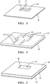
- Figure 4 illustrates the first substrate 22 on top of the conductive layer 32.
- the first substrate 22 comprises a dielectric layer and the first conductors 24 comprise vias in the first substrate 22.
- the first conductors 24 are open or empty vias while in other embodiments the vias are at least partially filled with a conductive material.
- one end of the substrate integrated waveguide formed by the first conductors 24 is aligned with the opening 52 to facilitate converting an electromagnetic wave propagating in the substrate integrated waveguide to an electromagnetic wave that propagates in the air-filled waveguide 30.
- Some of the first conductors 24 border three of the four sides of the opening 52 in this example.
- the fourth side of the opening 52 faces toward the port of the substrate integrated waveguide.
- Figure 5 shows the conductive layer 34 on an opposite side of the substrate 22 from the conductive layer 32.
- the conductive layer 34 includes an opening 58 aligned with the opening 52 of the conductive layer 32.
- the conductive layer 34 comprises a sheet of metal, such as copper and the opening 58 is established by etching away a corresponding portion of the layer 34.
- FIG 6 shows the adhesive layer 40 against the conductive layer 34.
- the conductive ribbon 44 is shown in contact with the adhesive layer 40.
- the conductive ribbon 44 in this example has the configuration of a rectangular frame that surrounds the area of the adhesive layer 40 that is aligned with the openings 52 and 58.
- the conductive ribbon 44 in some embodiments comprises a thin layer of copper.
- the conductive ribbon 44 functions as a cap for one side or end of the second conductors 28.
- the dimensions of the conductive ribbon 44 are selected to act as a band-stop filter to minimize or eliminate electromagnetic energy leakage into and through the nonconductive adhesive layer 40. Those skilled in the art who have the benefit of this description will be able to select a ribbon configuration and dimensions to meet their particular needs.
- Figure 7 shows the second substrate 26 situated on the adhesive layer 40.
- the second conductors 28 establish a border around the resonating cavity 50 that facilitates converting an electromagnetic wave propagating through the substrate integrated waveguide of the first substrate 22 into an electromagnetic wave propagating through the air-filled waveguide 30.
- the second conductors 28 comprise vias in the second substrate 26.
- the vias are empty or hollow while in others they are at least partially filled with a conductive material.
- Figure 8 illustrates the positional relationship among the conductors 28 and 24.
- the second conductors 28 that border the area aligned with the opening 52 are aligned with some of the first conductors 24 that border some of the opening 52.
- Those first conductors 24 are coaxial with corresponding ones of the second conductors 28.
- the first conductors 24a and 24b are respectively coaxially aligned with the second conductors 28a and 28b.
- the alignment of conductors can also be appreciated from Figures 1 and 2 . Others of the first conductors 24 that establish the fence of the substrate integrated waveguide in the substrate 22 are not aligned with second conductors 28 in the second substrate 26.
- One feature of the illustrated example is that the conductors 24 and 28 of the respective substrate layers do not have to be directly connected to each other. This provides a more economical manufacturing process and reduces overall cost. Securing the substrates 22 and 26 together using the adhesive 40 makes the manufacturing process for making the device 20 economical.
- the conductive ribbon 44 aligned with the second conductors 28 provides a cap to prevent leakage into or through the adhesive layer 40.
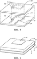
- Figure 9 shows a conductive layer 42 adjacent the second substrate 26 covering the second conductors 28 on a side of the second substrate 26 that is situated opposite the conductive ribbon 44 and facing away from the first substrate 22.
- the conductive layer 42 in some examples comprises a sheet of copper or another conductive metal.
- the second conductors 28 and the conductive layer 42 provide the backshort of the resonating cavity 50.
- the second substrate layer 26 in some examples includes a thickness that is selected to be approximately one-quarter of the wavelength of a signal frequency of interest in a system into which the signal handling device 20 will be incorporated. Such a substrate thickness is also appropriate for high efficiency antennas such that the device 20 lends itself to highly integrated packaging.
- Figure 10 illustrates another example embodiment that includes the additional feature of an antenna layer 70 on the second substrate 26 near the opening or port of the substrate integrated waveguide.
- Using the second conductors 28 and the second substrate 26 to form the resonating cavity or backshort of the device 20 provides a very wideband transition between the substrate integrated waveguide of the first substrate 22 and the air-filled waveguide 30. This is a significant advantage compared to other signal handling devices that have relatively poor bandwidth characteristics. Some embodiments designed consistent with the illustrated example provide a four-fold increase in bandwidth compared to prior devices.
Landscapes
- Engineering & Computer Science (AREA)
- Microelectronics & Electronic Packaging (AREA)
- Waveguides (AREA)
- Structure Of Printed Boards (AREA)
Abstract
Description
- A variety of scenarios require signal handling. For example, radar systems and wireless communication systems include over-the-air signaling. One challenge associated with such systems is providing adequate bandwidth in devices that handle such signals.
- Sufficient bandwidth is needed in radar systems to provide adequate range resolution. Higher bandwidth typically allows for higher range resolution, which enhances imaging and facilitates accurate target detection. In wireless communications, higher bandwidth corresponds to higher data rates allowing for enhanced services, such as video streaming and other data transfer.
- Some existing signal handling devices include a transition from a substrate integrated waveguide to an orthogonally oriented, air-filled waveguide. The bandwidth of such devices is typically very narrow resulting in poor manufacturability. One attempt at increasing the bandwidth for such devices has been to include metal plates to establish a resonating cavity. Such plates have to be particularly designed for particular applications, which introduces manufacturing inefficiencies. Additionally, such plates increase the cost of the device.
- A signal handling device includes a first substrate. A plurality of first conductors in the first substrate are arranged to form a substrate integrated waveguide. A second substrate includes a plurality of second conductors arranged to form a resonating cavity near one end of the substrate integrated waveguide. A signal carrier is aligned with the one end of the substrate integrated waveguide and the resonating cavity.
- In an example embodiment having one or more features of the signal handling device of the previous paragraph, the first substrate comprises a dielectric material, the first conductors comprise vias, the second substrate comprises a dielectric material, the second conductors comprise vias, and the signal carrier comprises a waveguide.
- In an example embodiment having one or more features of the signal handling device of any of the previous paragraphs, the waveguide comprises an air-filled waveguide.
- In an example embodiment having one or more features of the signal handling device of any of the previous paragraphs, the first substrate is planar, the second substrate is planar and parallel with the first substrate, the signal carrier is at least partially transverse to the first substrate.
- In an example embodiment having one or more features of the signal handling device of any of the previous paragraphs, the signal carrier is at least partially perpendicular to the first substrate.
- An example embodiment having one or more features of the signal handling device of any of the previous paragraphs includes a pressure sensitive adhesive aligned with one side of the first substrate and wherein at least a portion of one end of the signal carrier is secured to the pressure sensitive adhesive.
- An example embodiment having one or more features of the signal handling device of any of the previous paragraphs includes a first conductive layer on one side of the first substrate, the first conductive layer being in conductive contact with the first conductors, the first conductive layer including a first opening aligned with the one end of the substrate integrated waveguide; a second conductive layer on an oppositely facing side of the first substrate, the second conductive layer being in conductive contact with the first conductors, the second conductive layer including a second opening aligned with the first opening; an adhesive in contact with the second conductive layer, the adhesive securing the second substrate and the second conductive layer together; and a third conductive layer on a side of the second substrate that faces away from the first substrate, the third conductive layer being in conductive contact with the second conductors.
- An example embodiment having one or more features of the signal handling device of any of the previous paragraphs includes a conductive ribbon layer in contact with the adhesive layer and the second substrate, the conductive ribbon layer being aligned with and in conductive contact with the second conductors.
- In an example embodiment having one or more features of the signal handling device of any of the previous paragraphs, the conductive ribbon establishes a barrier to prevent signal leakage from the second conductors through the adhesive layer.
- In an example embodiment having one or more features of the signal handling device of any of the previous paragraphs, the conductive ribbon establishes a frame corresponding to a perimeter of the resonating cavity formed by the second conductors and the conductive ribbon has an opening aligned with the first and second openings.
- In an example embodiment having one or more features of the signal handling device of any of the previous paragraphs, the adhesive in contact with the second conductive layer comprises a fibrous material impregnated with a resin.
- In an example embodiment having one or more features of the signal handling device of any of the previous paragraphs, each of the conductive layers comprises metal.
- In an example embodiment having one or more features of the signal handling device of any of the previous paragraphs, the first opening is generally rectangular, the first opening has four sides, three sides of the first opening are bordered by at least some of the first conductors, the second opening is generally rectangular, and the second opening is surrounded by at least some of the second conductors.
- In an example embodiment having one or more features of the signal handling device of any of the previous paragraphs, the at least some of the first conductors that border the three sides of the first opening are coaxial with respective ones of the at least some of the second conductors.
- In an example embodiment having one or more features of the signal handling device of any of the previous paragraphs, others of the first conductors are arranged in two parallel lines and the others of the first conductors establish a fence of the substrate integrated waveguide.
- Various features and advantages of at least one disclosed example embodiment will become apparent to those skilled in the art from the following detailed description. The drawings that accompany the detailed description can be briefly described as follows.
-
-
Figure 1 diagrammatically illustrates a signal handling device designed according to an embodiment of this invention. -
Figure 2 is a cross-sectional illustration taken along the lines 2-2 inFigure 1 . -
Figure 3 diagrammatically illustrates a conductive layer useful in an embodiment of this invention. -
Figure 4 diagrammatically illustrates the conductive layer ofFigure 3 and a dielectric substrate layer including a substrate integrated waveguide. -
Figure 5 diagrammatically illustrates a conductive layer on top of the layers shown inFigure 4 . -
Figure 6 diagrammatically illustrates an adhesive layer and a conductive ribbon on top of the layers shown inFigure 5 . -
Figure 7 diagrammatically illustrates a dielectric substrate layer on top of the layers shown inFigure 6 in which the substrate includes conductors that form a resonating cavity. -
Figure 8 diagrammatically illustrates positional relationships among the conductors in the substrate layers of the example signal handling device. -
Figure 9 diagrammatically illustrates a conductive layer on top of the layers shown inFigure 7 . -
Figure 10 diagrammatically illustrates another example embodiment of a signal handling device. - A signal handling device designed according to an embodiment of this invention includes a resonating cavity formed by conductors in a dielectric substrate that facilitates propagating an electromagnetic wave from a substrate integrated waveguide to a transversely oriented waveguide. Embodiments of this invention increase bandwidth compared to previous devices that include a transition from a substrate integrated waveguide to an air-filled waveguide. For example, some embodiments provide up to four times the bandwidth available with previous signal handling devices.
-
Figures 1 and 2 diagrammatically illustrate asignal handling device 20 that may be used for a variety of purposes. One example use includes signal handling for devices mounted on an automotive vehicle. Some implementations are useful for automated vehicles that have autonomous or semi-autonomous vehicle control features. Another useful implementation of an embodiment of this invention is for wireless communications. - The example
signal handling device 20 includes afirst substrate 22 that comprises a dielectric material that is not conductive. As can be appreciated fromFigures 1 and 2 , thefirst substrate 22 includes a plurality offirst conductors 24 that are arranged to form a substrate integrated waveguide. Asecond substrate 26 comprises a dielectric material that is not conductive. Thesecond substrate 26 includes a plurality ofsecond conductors 28 that are arranged to form a resonating cavity or backshort near one end of the substrate integrated waveguide. - An air-filled
waveguide 30 is oriented at least partially transverse to thefirst substrate 22. In this example, the air-filledwaveguide 30 is oriented perpendicular to thefirst substrate 22. As shown inFigure 2 , a pressure sensitiveadhesive layer 36, which is not conductive, facilitates securing thewaveguide 30 to thefirst substrate 22. Thedevice 20 includes features that facilitate handling signals, such as electromagnetic waves, that propagate in the substrate integrated waveguide formed by thefirst conductors 24 and are converted to electromagnetic waves that propagate in the air-filledwaveguide 30. - The
first substrate 22 includes aconductive layer 32 on one side of thefirst substrate 22. Anotherconductive layer 34 is situated on an opposite side of thefirst substrate 22. Theconductive layers conductive layers first conductors 24. - An
adhesive layer 40 secures thesecond substrate 26 to theconductive layer 34 of thefirst substrate 22. Theadhesive layer 40 in the illustrated example embodiment comprises a nonconductive prepreg layer including a fibrous material impregnated with a resin. Aconductive layer 42 is situated on one side of thesecond substrate 26. Theconductive layer 42 contacts one end of thesecond conductors 28 and provides a cap over the resonatingcavity 50 established by thesecond conductors 28. - Another
conductive layer 44 is situated along a portion of an opposite side of theconductors 28 facing thefirst substrate 22. Theconductive layer 44 in this example comprises a ribbon of conductive metal, such as copper, that prevents electromagnetic leakage from thesecond conductors 28 into and through theadhesive layer 40. - The illustrated arrangement utilizes a substrate integrated waveguide formed by the
first conductors 24 in thefirst substrate 22 and a backshort or resonating cavity formed by thesecond conductors 28 in thesecond substrate 26. The resonatingcavity 50 is aligned with the air-filledwaveguide 30 of thedevice 20. That alignment facilitates converting an electromagnetic wave propagating through the substrate integrated waveguide into an electromagnetic wave propagating through the air-filledwaveguide 30. - A further understanding of the structure and arrangement of the
example device 20 can be appreciated by considering the different layers of the device and how they are arranged relative to each other.Figure 3 illustrates an exampleconductive layer 32, such as a sheet of copper. In this example, theconductive layer 32 includes anopening 52 that is aligned with thewaveguide 30 in the fully assembleddevice 20. Theopening 52 may be established, for example, by etching away a corresponding area of theconductive layer 32. The illustratedexample opening 52 includestabs 54 that are dimensioned to provide microwave matching structures. Those skilled in the art who have the benefit of this description will understand how the dimensions of theopening 52 and thetabs 54 may be selected or tuned to control the coupling between the substrate integrated waveguide of thefirst substrate 22 and thewaveguide 30. The dimensions or configuration of theopening 52 may also serve as a secondary adjustment of frequency. -
Figure 4 illustrates thefirst substrate 22 on top of theconductive layer 32. In this example, thefirst substrate 22 comprises a dielectric layer and thefirst conductors 24 comprise vias in thefirst substrate 22. In some example embodiments, thefirst conductors 24 are open or empty vias while in other embodiments the vias are at least partially filled with a conductive material. - As shown in
Figure 4 , one end of the substrate integrated waveguide formed by thefirst conductors 24 is aligned with theopening 52 to facilitate converting an electromagnetic wave propagating in the substrate integrated waveguide to an electromagnetic wave that propagates in the air-filledwaveguide 30. Some of thefirst conductors 24 border three of the four sides of theopening 52 in this example. The fourth side of theopening 52 faces toward the port of the substrate integrated waveguide. -
Figure 5 shows theconductive layer 34 on an opposite side of thesubstrate 22 from theconductive layer 32. Theconductive layer 34 includes anopening 58 aligned with theopening 52 of theconductive layer 32. In some embodiments, theconductive layer 34 comprises a sheet of metal, such as copper and theopening 58 is established by etching away a corresponding portion of thelayer 34. -
Figure 6 shows theadhesive layer 40 against theconductive layer 34. InFigure 6 , theconductive ribbon 44 is shown in contact with theadhesive layer 40. Theconductive ribbon 44 in this example has the configuration of a rectangular frame that surrounds the area of theadhesive layer 40 that is aligned with theopenings conductive ribbon 44 in some embodiments comprises a thin layer of copper. Theconductive ribbon 44 functions as a cap for one side or end of thesecond conductors 28. The dimensions of theconductive ribbon 44 are selected to act as a band-stop filter to minimize or eliminate electromagnetic energy leakage into and through the nonconductiveadhesive layer 40. Those skilled in the art who have the benefit of this description will be able to select a ribbon configuration and dimensions to meet their particular needs. -
Figure 7 shows thesecond substrate 26 situated on theadhesive layer 40. Thesecond conductors 28 establish a border around the resonatingcavity 50 that facilitates converting an electromagnetic wave propagating through the substrate integrated waveguide of thefirst substrate 22 into an electromagnetic wave propagating through the air-filledwaveguide 30. - In the illustrated example, the
second conductors 28 comprise vias in thesecond substrate 26. In some embodiments, the vias are empty or hollow while in others they are at least partially filled with a conductive material. -
Figure 8 illustrates the positional relationship among theconductors second conductors 28 that border the area aligned with theopening 52 are aligned with some of thefirst conductors 24 that border some of theopening 52. Thosefirst conductors 24 are coaxial with corresponding ones of thesecond conductors 28. For example, the first conductors 24a and 24b are respectively coaxially aligned with the second conductors 28a and 28b. The alignment of conductors can also be appreciated fromFigures 1 and 2 . Others of thefirst conductors 24 that establish the fence of the substrate integrated waveguide in thesubstrate 22 are not aligned withsecond conductors 28 in thesecond substrate 26. - One feature of the illustrated example is that the
conductors substrates device 20 economical. Theconductive ribbon 44 aligned with thesecond conductors 28 provides a cap to prevent leakage into or through theadhesive layer 40. -
Figure 9 shows aconductive layer 42 adjacent thesecond substrate 26 covering thesecond conductors 28 on a side of thesecond substrate 26 that is situated opposite theconductive ribbon 44 and facing away from thefirst substrate 22. Theconductive layer 42 in some examples comprises a sheet of copper or another conductive metal. Thesecond conductors 28 and theconductive layer 42 provide the backshort of the resonatingcavity 50. - The
second substrate layer 26 in some examples includes a thickness that is selected to be approximately one-quarter of the wavelength of a signal frequency of interest in a system into which thesignal handling device 20 will be incorporated. Such a substrate thickness is also appropriate for high efficiency antennas such that thedevice 20 lends itself to highly integrated packaging. -
Figure 10 illustrates another example embodiment that includes the additional feature of anantenna layer 70 on thesecond substrate 26 near the opening or port of the substrate integrated waveguide. - Using the
second conductors 28 and thesecond substrate 26 to form the resonating cavity or backshort of thedevice 20 provides a very wideband transition between the substrate integrated waveguide of thefirst substrate 22 and the air-filledwaveguide 30. This is a significant advantage compared to other signal handling devices that have relatively poor bandwidth characteristics. Some embodiments designed consistent with the illustrated example provide a four-fold increase in bandwidth compared to prior devices. - The preceding description is exemplary rather than limiting in nature. Variations and modifications to the disclosed examples may become apparent to those skilled in the art that do not necessarily depart from the essence of this invention. The scope of legal protection given to this invention can only be determined by studying the following claims.
Claims (15)
- A signal handling device (20), comprising:a first substrate (22);a plurality of first conductors (24) in the first substrate (22), the first conductors (24) being arranged to form a substrate integrated waveguide;a second substrate (26);a plurality of second conductors (28) in the second substrate (26), the second conductors (28) being arranged to form a resonating cavity (50) near one end of the substrate integrated waveguide; anda signal carrier (30) aligned with the one end of the substrate integrated waveguide.
- The signal handling device (20) of claim 1, wherein
the first substrate (22) comprises a dielectric material;
the first conductors (24) comprise vias;
the second substrate (26) comprises a dielectric material;
the second conductors (28) comprise vias; and
the signal carrier (30) comprises a waveguide. - The signal handling device (20) of claim 2, wherein the waveguide comprises an air-filled waveguide.
- The signal handling device (20) according to any one of the preceding claims, wherein
the first substrate (22) is planar;
the second substrate (26) is planar and parallel with the first substrate (22);
the signal carrier (30) is at least partially transverse to the first substrate (22). - The signal handling device (20) of claim 4, wherein the signal carrier (30) is at least partially perpendicular to the first substrate (22).
- The signal handling device (20) according to any one of the preceding claims, comprising a pressure sensitive adhesive (40) aligned with one side of the first substrate (22) and wherein at least a portion of one end of the signal carrier (30) is secured to the pressure sensitive adhesive (40).
- The signal handling device (20) according to any one of the preceding claims, comprising
a first conductive layer (32) on one side of the first substrate (22), the first conductive layer (32) being in conductive contact with the first conductors (24), the first conductive layer (32) including a first opening aligned with the one end of the substrate integrated waveguide;
a second conductive layer (42) on an oppositely facing side of the first substrate (22), the second conductive layer (42) being in conductive contact with the first conductors (24), the second conductive layer (42) including a second opening aligned with the first opening;
an adhesive (40) in contact with the second conductive layer (42), the adhesive (40) securing the second substrate (26) and the second conductive layer (42) together; and
a third conductive layer (44) on a side of the second substrate (26) that faces away from the first substrate (22), the third conductive layer (44) being in conductive contact with the second conductors (28). - The signal handling device (20) of claim 7, comprising a conductive ribbon layer (44) in contact with the adhesive (40) and the second substrate (26), the conductive ribbon layer (44) being aligned with and in conductive contact with the second conductors (28).
- The signal handling device (20) of claim 8, wherein the conductive ribbon layer (44) establishes a barrier to prevent signal leakage from the second conductors (28) through the adhesive (40).
- The signal handling device (20) of claim 8, wherein
the conductive ribbon layer (44) establishes a frame corresponding to a perimeter of the resonating cavity (50) formed by the second conductors (28); and
the conductive ribbon layer (44) has an opening aligned with the first and second openings. - The signal handling device (20) according to any one of the claims 7 to 10, wherein the adhesive (40) in contact with the second conductive layer (34) comprises a fibrous material impregnated with a resin.
- The signal handling device (20) according to any one of the claims 7 to 11, wherein each of the conductive layers comprises metal.
- The signal handling device (20) according to any one of the claims 7 to 12, wherein
the first opening is generally rectangular;
the first opening has four sides;
three sides of the first opening are bordered by at least some of the first conductors (24);
the second opening is generally rectangular; and
the second opening is bordered by at least some of the second conductors (28). - The signal handling device (20) of claim 13, wherein the at least some of the first conductors (24) that border the three sides of the first opening are coaxial with respective ones of the at least some of the second conductors (28).
- The signal handling device (20) according to any one of the claims 13 and 14, wherein
others of the first conductors (24) are arranged in two parallel lines; and the others of the first conductors (24) establish a fence of the substrate integrated waveguide.
Applications Claiming Priority (2)
| Application Number | Priority Date | Filing Date | Title |
|---|---|---|---|
| US201862628038P | 2018-02-08 | 2018-02-08 | |
| US15/934,126 US10680305B2 (en) | 2018-02-08 | 2018-03-23 | Signal handling device including a surface integrated waveguide and a resonating cavity formed in multiple substrate layers |
Publications (2)
| Publication Number | Publication Date |
|---|---|
| EP3525282A1 true EP3525282A1 (en) | 2019-08-14 |
| EP3525282B1 EP3525282B1 (en) | 2022-07-20 |
Family
ID=65228460
Family Applications (1)
| Application Number | Title | Priority Date | Filing Date |
|---|---|---|---|
| EP19153509.5A Active EP3525282B1 (en) | 2018-02-08 | 2019-01-24 | Signal handling device including multiple substrate layers |
Country Status (3)
| Country | Link |
|---|---|
| US (1) | US10680305B2 (en) |
| EP (1) | EP3525282B1 (en) |
| CN (1) | CN110137652B (en) |
Families Citing this family (6)
| Publication number | Priority date | Publication date | Assignee | Title |
|---|---|---|---|---|
| WO2019235120A1 (en) * | 2018-06-04 | 2019-12-12 | 日本電気株式会社 | Connection structure for dielectric waveguide line and waveguide |
| JP7402035B2 (en) * | 2019-12-18 | 2023-12-20 | Jrcモビリティ株式会社 | waveguide converter |
| JP7294191B2 (en) * | 2020-03-06 | 2023-06-20 | 株式会社デンソー | Double-sided board, radar device, transmission member, and method for manufacturing transmission member |
| EP4016620A1 (en) | 2020-12-16 | 2022-06-22 | Nxp B.V. | Package with an integrated circuit die and a waveguide launcher |
| CN113193347B (en) * | 2021-04-14 | 2022-05-03 | 电子科技大学 | Dual-beam cavity-backed antenna based on artificial electromagnetic structure and cavity odd-mode excitation |
| US20230352841A1 (en) * | 2022-05-02 | 2023-11-02 | Texas Instruments Incorporated | Wireless system package |
Citations (5)
| Publication number | Priority date | Publication date | Assignee | Title |
|---|---|---|---|---|
| EP1195839A1 (en) * | 2000-10-06 | 2002-04-10 | Mitsubishi Denki Kabushiki Kaisha | Waveguide coupler |
| JP2004135095A (en) * | 2002-10-10 | 2004-04-30 | Mitsubishi Electric Corp | Waveguide / microstrip line converter |
| US20080309427A1 (en) * | 2005-12-08 | 2008-12-18 | Electronics And Telecommunications Research Institute | Transit Structure of Standard Waveguide and Dielectric Waveguide |
| EP2426782A1 (en) * | 2009-04-28 | 2012-03-07 | Mitsubishi Electric Corporation | Waveguide conversion portion connection structure, method of fabricating same, and antenna device using this connection structure |
| US20120319796A1 (en) * | 2010-02-17 | 2012-12-20 | Nec Corporation | Waveguide/planar line transducer |
Family Cites Families (7)
| Publication number | Priority date | Publication date | Assignee | Title |
|---|---|---|---|---|
| JP5179513B2 (en) * | 2007-12-28 | 2013-04-10 | 京セラ株式会社 | High-frequency transmission line connection structure, wiring board, high-frequency module, and radar device |
| CN201383535Y (en) * | 2009-04-01 | 2010-01-13 | 惠州市硕贝德通讯科技有限公司 | Rectangular waveguide-substrate integrated waveguide signal conversion and power divider |
| JP5476873B2 (en) * | 2009-09-05 | 2014-04-23 | 富士通株式会社 | Signal converter and manufacturing method thereof |
| KR101761920B1 (en) * | 2011-02-16 | 2017-07-26 | 삼성전기주식회사 | Dielectric waveguide antenna |
| JP6059746B2 (en) * | 2015-02-09 | 2017-01-11 | 株式会社フジクラ | converter |
| CN105609909A (en) * | 2016-03-08 | 2016-05-25 | 电子科技大学 | Device for transition from rectangular waveguide to substrate integrated waveguide on Ka-band |
| US10468736B2 (en) * | 2017-02-08 | 2019-11-05 | Aptiv Technologies Limited | Radar assembly with ultra wide band waveguide to substrate integrated waveguide transition |
-
2018
- 2018-03-23 US US15/934,126 patent/US10680305B2/en active Active
-
2019
- 2019-01-24 EP EP19153509.5A patent/EP3525282B1/en active Active
- 2019-02-11 CN CN201910110072.4A patent/CN110137652B/en active Active
Patent Citations (5)
| Publication number | Priority date | Publication date | Assignee | Title |
|---|---|---|---|---|
| EP1195839A1 (en) * | 2000-10-06 | 2002-04-10 | Mitsubishi Denki Kabushiki Kaisha | Waveguide coupler |
| JP2004135095A (en) * | 2002-10-10 | 2004-04-30 | Mitsubishi Electric Corp | Waveguide / microstrip line converter |
| US20080309427A1 (en) * | 2005-12-08 | 2008-12-18 | Electronics And Telecommunications Research Institute | Transit Structure of Standard Waveguide and Dielectric Waveguide |
| EP2426782A1 (en) * | 2009-04-28 | 2012-03-07 | Mitsubishi Electric Corporation | Waveguide conversion portion connection structure, method of fabricating same, and antenna device using this connection structure |
| US20120319796A1 (en) * | 2010-02-17 | 2012-12-20 | Nec Corporation | Waveguide/planar line transducer |
Also Published As
| Publication number | Publication date |
|---|---|
| US10680305B2 (en) | 2020-06-09 |
| EP3525282B1 (en) | 2022-07-20 |
| CN110137652A (en) | 2019-08-16 |
| CN110137652B (en) | 2021-08-24 |
| US20190245257A1 (en) | 2019-08-08 |
Similar Documents
| Publication | Publication Date | Title |
|---|---|---|
| EP3525282B1 (en) | Signal handling device including multiple substrate layers | |
| US11670829B2 (en) | Radar assembly with rectangular waveguide to substrate integrated waveguide transition | |
| US9401532B2 (en) | High-frequency signal line and electronic device including the same | |
| US20210313703A1 (en) | Millimeter-Wave Antenna Array Element, Array Antenna, and Communications Product | |
| US8860607B2 (en) | Gain enhanced LTCC system-on-package for UMRR applications | |
| US9402301B2 (en) | Vertical radio frequency module | |
| US9455486B2 (en) | Integrated circulator for phased arrays | |
| US20200119423A1 (en) | Connection structure between waveguide and coaxial cable | |
| KR102532709B1 (en) | Wideband antenna system | |
| US11056777B2 (en) | Millimeter wave LTCC filter | |
| EP3780279A1 (en) | Array antenna apparatus and communication device | |
| US8344820B1 (en) | Integrated circulator for phased arrays | |
| US12394904B2 (en) | Metasurface for smartphone antenna, and smartphone device comprising same | |
| US11223119B2 (en) | Millimeter wave LTCC filter | |
| US8810332B2 (en) | Electromagnetic coupler and information communication device with same mounted thereon | |
| US12476355B2 (en) | System | |
| US11621464B2 (en) | Waveguide assembly | |
| KR20220163282A (en) | Compact low-profile aperture antenna with integrated diplexer | |
| US20160006099A1 (en) | Wideband transition between a planar transmission line and a waveguide | |
| KR101838592B1 (en) | Circulator with lamination layers of multiple substrates | |
| JP4172791B2 (en) | Transmission line and high frequency module | |
| KR102198378B1 (en) | Switched beam-forming antenna device and manufacturing method thereof | |
| CN211507855U (en) | Filter assembly and coupler thereof | |
| Dash et al. | Antennas for Full-Duplex Communication: State of the Art and Way Forward | |
| Lee | Silicon-Based Antenna and Circuit Co-Integration for Emerging RF/Mm-Wave Applications |
Legal Events
| Date | Code | Title | Description |
|---|---|---|---|
| PUAI | Public reference made under article 153(3) epc to a published international application that has entered the european phase |
Free format text: ORIGINAL CODE: 0009012 |
|
| STAA | Information on the status of an ep patent application or granted ep patent |
Free format text: STATUS: THE APPLICATION HAS BEEN PUBLISHED |
|
| AK | Designated contracting states |
Kind code of ref document: A1 Designated state(s): AL AT BE BG CH CY CZ DE DK EE ES FI FR GB GR HR HU IE IS IT LI LT LU LV MC MK MT NL NO PL PT RO RS SE SI SK SM TR |
|
| AX | Request for extension of the european patent |
Extension state: BA ME |
|
| STAA | Information on the status of an ep patent application or granted ep patent |
Free format text: STATUS: REQUEST FOR EXAMINATION WAS MADE |
|
| 17P | Request for examination filed |
Effective date: 20200214 |
|
| RBV | Designated contracting states (corrected) |
Designated state(s): AL AT BE BG CH CY CZ DE DK EE ES FI FR GB GR HR HU IE IS IT LI LT LU LV MC MK MT NL NO PL PT RO RS SE SI SK SM TR |
|
| STAA | Information on the status of an ep patent application or granted ep patent |
Free format text: STATUS: EXAMINATION IS IN PROGRESS |
|
| 17Q | First examination report despatched |
Effective date: 20210126 |
|
| GRAP | Despatch of communication of intention to grant a patent |
Free format text: ORIGINAL CODE: EPIDOSNIGR1 |
|
| STAA | Information on the status of an ep patent application or granted ep patent |
Free format text: STATUS: GRANT OF PATENT IS INTENDED |
|
| INTG | Intention to grant announced |
Effective date: 20220215 |
|
| GRAS | Grant fee paid |
Free format text: ORIGINAL CODE: EPIDOSNIGR3 |
|
| GRAA | (expected) grant |
Free format text: ORIGINAL CODE: 0009210 |
|
| STAA | Information on the status of an ep patent application or granted ep patent |
Free format text: STATUS: THE PATENT HAS BEEN GRANTED |
|
| AK | Designated contracting states |
Kind code of ref document: B1 Designated state(s): AL AT BE BG CH CY CZ DE DK EE ES FI FR GB GR HR HU IE IS IT LI LT LU LV MC MK MT NL NO PL PT RO RS SE SI SK SM TR |
|
| REG | Reference to a national code |
Ref country code: CH Ref legal event code: EP |
|
| REG | Reference to a national code |
Ref country code: DE Ref legal event code: R096 Ref document number: 602019017080 Country of ref document: DE |
|
| REG | Reference to a national code |
Ref country code: AT Ref legal event code: REF Ref document number: 1506133 Country of ref document: AT Kind code of ref document: T Effective date: 20220815 |
|
| REG | Reference to a national code |
Ref country code: IE Ref legal event code: FG4D |
|
| REG | Reference to a national code |
Ref country code: LT Ref legal event code: MG9D |
|
| REG | Reference to a national code |
Ref country code: NL Ref legal event code: MP Effective date: 20220720 |
|
| PG25 | Lapsed in a contracting state [announced via postgrant information from national office to epo] |
Ref country code: SE Free format text: LAPSE BECAUSE OF FAILURE TO SUBMIT A TRANSLATION OF THE DESCRIPTION OR TO PAY THE FEE WITHIN THE PRESCRIBED TIME-LIMIT Effective date: 20220720 Ref country code: RS Free format text: LAPSE BECAUSE OF FAILURE TO SUBMIT A TRANSLATION OF THE DESCRIPTION OR TO PAY THE FEE WITHIN THE PRESCRIBED TIME-LIMIT Effective date: 20220720 Ref country code: PT Free format text: LAPSE BECAUSE OF FAILURE TO SUBMIT A TRANSLATION OF THE DESCRIPTION OR TO PAY THE FEE WITHIN THE PRESCRIBED TIME-LIMIT Effective date: 20221121 Ref country code: NO Free format text: LAPSE BECAUSE OF FAILURE TO SUBMIT A TRANSLATION OF THE DESCRIPTION OR TO PAY THE FEE WITHIN THE PRESCRIBED TIME-LIMIT Effective date: 20221020 Ref country code: NL Free format text: LAPSE BECAUSE OF FAILURE TO SUBMIT A TRANSLATION OF THE DESCRIPTION OR TO PAY THE FEE WITHIN THE PRESCRIBED TIME-LIMIT Effective date: 20220720 Ref country code: LV Free format text: LAPSE BECAUSE OF FAILURE TO SUBMIT A TRANSLATION OF THE DESCRIPTION OR TO PAY THE FEE WITHIN THE PRESCRIBED TIME-LIMIT Effective date: 20220720 Ref country code: LT Free format text: LAPSE BECAUSE OF FAILURE TO SUBMIT A TRANSLATION OF THE DESCRIPTION OR TO PAY THE FEE WITHIN THE PRESCRIBED TIME-LIMIT Effective date: 20220720 Ref country code: FI Free format text: LAPSE BECAUSE OF FAILURE TO SUBMIT A TRANSLATION OF THE DESCRIPTION OR TO PAY THE FEE WITHIN THE PRESCRIBED TIME-LIMIT Effective date: 20220720 Ref country code: ES Free format text: LAPSE BECAUSE OF FAILURE TO SUBMIT A TRANSLATION OF THE DESCRIPTION OR TO PAY THE FEE WITHIN THE PRESCRIBED TIME-LIMIT Effective date: 20220720 |
|
| REG | Reference to a national code |
Ref country code: AT Ref legal event code: MK05 Ref document number: 1506133 Country of ref document: AT Kind code of ref document: T Effective date: 20220720 |
|
| PG25 | Lapsed in a contracting state [announced via postgrant information from national office to epo] |
Ref country code: PL Free format text: LAPSE BECAUSE OF FAILURE TO SUBMIT A TRANSLATION OF THE DESCRIPTION OR TO PAY THE FEE WITHIN THE PRESCRIBED TIME-LIMIT Effective date: 20220720 Ref country code: IS Free format text: LAPSE BECAUSE OF FAILURE TO SUBMIT A TRANSLATION OF THE DESCRIPTION OR TO PAY THE FEE WITHIN THE PRESCRIBED TIME-LIMIT Effective date: 20221120 Ref country code: HR Free format text: LAPSE BECAUSE OF FAILURE TO SUBMIT A TRANSLATION OF THE DESCRIPTION OR TO PAY THE FEE WITHIN THE PRESCRIBED TIME-LIMIT Effective date: 20220720 Ref country code: GR Free format text: LAPSE BECAUSE OF FAILURE TO SUBMIT A TRANSLATION OF THE DESCRIPTION OR TO PAY THE FEE WITHIN THE PRESCRIBED TIME-LIMIT Effective date: 20221021 |
|
| RAP4 | Party data changed (patent owner data changed or rights of a patent transferred) |
Owner name: APTIV TECHNOLOGIES LIMITED |
|
| REG | Reference to a national code |
Ref country code: DE Ref legal event code: R097 Ref document number: 602019017080 Country of ref document: DE |
|
| PG25 | Lapsed in a contracting state [announced via postgrant information from national office to epo] |
Ref country code: SM Free format text: LAPSE BECAUSE OF FAILURE TO SUBMIT A TRANSLATION OF THE DESCRIPTION OR TO PAY THE FEE WITHIN THE PRESCRIBED TIME-LIMIT Effective date: 20220720 Ref country code: RO Free format text: LAPSE BECAUSE OF FAILURE TO SUBMIT A TRANSLATION OF THE DESCRIPTION OR TO PAY THE FEE WITHIN THE PRESCRIBED TIME-LIMIT Effective date: 20220720 Ref country code: DK Free format text: LAPSE BECAUSE OF FAILURE TO SUBMIT A TRANSLATION OF THE DESCRIPTION OR TO PAY THE FEE WITHIN THE PRESCRIBED TIME-LIMIT Effective date: 20220720 Ref country code: CZ Free format text: LAPSE BECAUSE OF FAILURE TO SUBMIT A TRANSLATION OF THE DESCRIPTION OR TO PAY THE FEE WITHIN THE PRESCRIBED TIME-LIMIT Effective date: 20220720 Ref country code: AT Free format text: LAPSE BECAUSE OF FAILURE TO SUBMIT A TRANSLATION OF THE DESCRIPTION OR TO PAY THE FEE WITHIN THE PRESCRIBED TIME-LIMIT Effective date: 20220720 |
|
| PLBE | No opposition filed within time limit |
Free format text: ORIGINAL CODE: 0009261 |
|
| STAA | Information on the status of an ep patent application or granted ep patent |
Free format text: STATUS: NO OPPOSITION FILED WITHIN TIME LIMIT |
|
| PG25 | Lapsed in a contracting state [announced via postgrant information from national office to epo] |
Ref country code: SK Free format text: LAPSE BECAUSE OF FAILURE TO SUBMIT A TRANSLATION OF THE DESCRIPTION OR TO PAY THE FEE WITHIN THE PRESCRIBED TIME-LIMIT Effective date: 20220720 Ref country code: EE Free format text: LAPSE BECAUSE OF FAILURE TO SUBMIT A TRANSLATION OF THE DESCRIPTION OR TO PAY THE FEE WITHIN THE PRESCRIBED TIME-LIMIT Effective date: 20220720 |
|
| P01 | Opt-out of the competence of the unified patent court (upc) registered |
Effective date: 20230424 |
|
| 26N | No opposition filed |
Effective date: 20230421 |
|
| PG25 | Lapsed in a contracting state [announced via postgrant information from national office to epo] |
Ref country code: AL Free format text: LAPSE BECAUSE OF FAILURE TO SUBMIT A TRANSLATION OF THE DESCRIPTION OR TO PAY THE FEE WITHIN THE PRESCRIBED TIME-LIMIT Effective date: 20220720 |
|
| PG25 | Lapsed in a contracting state [announced via postgrant information from national office to epo] |
Ref country code: SI Free format text: LAPSE BECAUSE OF FAILURE TO SUBMIT A TRANSLATION OF THE DESCRIPTION OR TO PAY THE FEE WITHIN THE PRESCRIBED TIME-LIMIT Effective date: 20220720 |
|
| REG | Reference to a national code |
Ref country code: CH Ref legal event code: PL |
|
| PG25 | Lapsed in a contracting state [announced via postgrant information from national office to epo] |
Ref country code: LU Free format text: LAPSE BECAUSE OF NON-PAYMENT OF DUE FEES Effective date: 20230124 |
|
| REG | Reference to a national code |
Ref country code: BE Ref legal event code: MM Effective date: 20230131 |
|
| PG25 | Lapsed in a contracting state [announced via postgrant information from national office to epo] |
Ref country code: LI Free format text: LAPSE BECAUSE OF NON-PAYMENT OF DUE FEES Effective date: 20230131 Ref country code: CH Free format text: LAPSE BECAUSE OF NON-PAYMENT OF DUE FEES Effective date: 20230131 |
|
| PG25 | Lapsed in a contracting state [announced via postgrant information from national office to epo] |
Ref country code: BE Free format text: LAPSE BECAUSE OF NON-PAYMENT OF DUE FEES Effective date: 20230131 |
|
| PG25 | Lapsed in a contracting state [announced via postgrant information from national office to epo] |
Ref country code: IE Free format text: LAPSE BECAUSE OF NON-PAYMENT OF DUE FEES Effective date: 20230124 |
|
| PG25 | Lapsed in a contracting state [announced via postgrant information from national office to epo] |
Ref country code: IT Free format text: LAPSE BECAUSE OF FAILURE TO SUBMIT A TRANSLATION OF THE DESCRIPTION OR TO PAY THE FEE WITHIN THE PRESCRIBED TIME-LIMIT Effective date: 20220720 |
|
| PG25 | Lapsed in a contracting state [announced via postgrant information from national office to epo] |
Ref country code: MC Free format text: LAPSE BECAUSE OF FAILURE TO SUBMIT A TRANSLATION OF THE DESCRIPTION OR TO PAY THE FEE WITHIN THE PRESCRIBED TIME-LIMIT Effective date: 20220720 |
|
| PG25 | Lapsed in a contracting state [announced via postgrant information from national office to epo] |
Ref country code: MC Free format text: LAPSE BECAUSE OF FAILURE TO SUBMIT A TRANSLATION OF THE DESCRIPTION OR TO PAY THE FEE WITHIN THE PRESCRIBED TIME-LIMIT Effective date: 20220720 |
|
| PG25 | Lapsed in a contracting state [announced via postgrant information from national office to epo] |
Ref country code: BG Free format text: LAPSE BECAUSE OF FAILURE TO SUBMIT A TRANSLATION OF THE DESCRIPTION OR TO PAY THE FEE WITHIN THE PRESCRIBED TIME-LIMIT Effective date: 20220720 |
|
| PG25 | Lapsed in a contracting state [announced via postgrant information from national office to epo] |
Ref country code: BG Free format text: LAPSE BECAUSE OF FAILURE TO SUBMIT A TRANSLATION OF THE DESCRIPTION OR TO PAY THE FEE WITHIN THE PRESCRIBED TIME-LIMIT Effective date: 20220720 |
|
| REG | Reference to a national code |
Ref country code: DE Ref legal event code: R081 Ref document number: 602019017080 Country of ref document: DE Owner name: APTIV TECHNOLOGIES AG, CH Free format text: FORMER OWNER: APTIV TECHNOLOGIES LIMITED, ST. MICHAEL, BB |
|
| PG25 | Lapsed in a contracting state [announced via postgrant information from national office to epo] |
Ref country code: CY Free format text: LAPSE BECAUSE OF FAILURE TO SUBMIT A TRANSLATION OF THE DESCRIPTION OR TO PAY THE FEE WITHIN THE PRESCRIBED TIME-LIMIT; INVALID AB INITIO Effective date: 20190124 |
|
| PG25 | Lapsed in a contracting state [announced via postgrant information from national office to epo] |
Ref country code: HU Free format text: LAPSE BECAUSE OF FAILURE TO SUBMIT A TRANSLATION OF THE DESCRIPTION OR TO PAY THE FEE WITHIN THE PRESCRIBED TIME-LIMIT; INVALID AB INITIO Effective date: 20190124 |
|
| PG25 | Lapsed in a contracting state [announced via postgrant information from national office to epo] |
Ref country code: TR Free format text: LAPSE BECAUSE OF FAILURE TO SUBMIT A TRANSLATION OF THE DESCRIPTION OR TO PAY THE FEE WITHIN THE PRESCRIBED TIME-LIMIT Effective date: 20220720 |
|
| PGFP | Annual fee paid to national office [announced via postgrant information from national office to epo] |
Ref country code: GB Payment date: 20260112 Year of fee payment: 8 |
|
| PGFP | Annual fee paid to national office [announced via postgrant information from national office to epo] |
Ref country code: DE Payment date: 20251217 Year of fee payment: 8 |
|
| PGFP | Annual fee paid to national office [announced via postgrant information from national office to epo] |
Ref country code: FR Payment date: 20260107 Year of fee payment: 8 |