EP3525241A2 - Organic light-emitting display device - Google Patents
Organic light-emitting display device Download PDFInfo
- Publication number
- EP3525241A2 EP3525241A2 EP19156098.6A EP19156098A EP3525241A2 EP 3525241 A2 EP3525241 A2 EP 3525241A2 EP 19156098 A EP19156098 A EP 19156098A EP 3525241 A2 EP3525241 A2 EP 3525241A2
- Authority
- EP
- European Patent Office
- Prior art keywords
- organic light
- display device
- layer
- emitting display
- sensing lines
- Prior art date
- Legal status (The legal status is an assumption and is not a legal conclusion. Google has not performed a legal analysis and makes no representation as to the accuracy of the status listed.)
- Granted
Links
Images






Classifications
-
- G—PHYSICS
- G06—COMPUTING OR CALCULATING; COUNTING
- G06F—ELECTRIC DIGITAL DATA PROCESSING
- G06F3/00—Input arrangements for transferring data to be processed into a form capable of being handled by the computer; Output arrangements for transferring data from processing unit to output unit, e.g. interface arrangements
- G06F3/01—Input arrangements or combined input and output arrangements for interaction between user and computer
- G06F3/03—Arrangements for converting the position or the displacement of a member into a coded form
- G06F3/041—Digitisers, e.g. for touch screens or touch pads, characterised by the transducing means
- G06F3/0412—Digitisers structurally integrated in a display
-
- G—PHYSICS
- G06—COMPUTING OR CALCULATING; COUNTING
- G06F—ELECTRIC DIGITAL DATA PROCESSING
- G06F3/00—Input arrangements for transferring data to be processed into a form capable of being handled by the computer; Output arrangements for transferring data from processing unit to output unit, e.g. interface arrangements
- G06F3/01—Input arrangements or combined input and output arrangements for interaction between user and computer
- G06F3/03—Arrangements for converting the position or the displacement of a member into a coded form
- G06F3/041—Digitisers, e.g. for touch screens or touch pads, characterised by the transducing means
- G06F3/044—Digitisers, e.g. for touch screens or touch pads, characterised by the transducing means by capacitive means
-
- G—PHYSICS
- G06—COMPUTING OR CALCULATING; COUNTING
- G06F—ELECTRIC DIGITAL DATA PROCESSING
- G06F3/00—Input arrangements for transferring data to be processed into a form capable of being handled by the computer; Output arrangements for transferring data from processing unit to output unit, e.g. interface arrangements
- G06F3/01—Input arrangements or combined input and output arrangements for interaction between user and computer
- G06F3/03—Arrangements for converting the position or the displacement of a member into a coded form
- G06F3/041—Digitisers, e.g. for touch screens or touch pads, characterised by the transducing means
- G06F3/044—Digitisers, e.g. for touch screens or touch pads, characterised by the transducing means by capacitive means
- G06F3/0446—Digitisers, e.g. for touch screens or touch pads, characterised by the transducing means by capacitive means using a grid-like structure of electrodes in at least two directions, e.g. using row and column electrodes
-
- H—ELECTRICITY
- H10—SEMICONDUCTOR DEVICES; ELECTRIC SOLID-STATE DEVICES NOT OTHERWISE PROVIDED FOR
- H10K—ORGANIC ELECTRIC SOLID-STATE DEVICES
- H10K50/00—Organic light-emitting devices
- H10K50/80—Constructional details
- H10K50/805—Electrodes
- H10K50/82—Cathodes
- H10K50/822—Cathodes characterised by their shape
-
- H—ELECTRICITY
- H10—SEMICONDUCTOR DEVICES; ELECTRIC SOLID-STATE DEVICES NOT OTHERWISE PROVIDED FOR
- H10K—ORGANIC ELECTRIC SOLID-STATE DEVICES
- H10K50/00—Organic light-emitting devices
- H10K50/80—Constructional details
- H10K50/86—Arrangements for improving contrast, e.g. preventing reflection of ambient light
- H10K50/865—Arrangements for improving contrast, e.g. preventing reflection of ambient light comprising light absorbing layers, e.g. light-blocking layers
-
- H—ELECTRICITY
- H10—SEMICONDUCTOR DEVICES; ELECTRIC SOLID-STATE DEVICES NOT OTHERWISE PROVIDED FOR
- H10K—ORGANIC ELECTRIC SOLID-STATE DEVICES
- H10K59/00—Integrated devices, or assemblies of multiple devices, comprising at least one organic light-emitting element covered by group H10K50/00
- H10K59/10—OLED displays
- H10K59/12—Active-matrix OLED [AMOLED] displays
- H10K59/121—Active-matrix OLED [AMOLED] displays characterised by the geometry or disposition of pixel elements
-
- H—ELECTRICITY
- H10—SEMICONDUCTOR DEVICES; ELECTRIC SOLID-STATE DEVICES NOT OTHERWISE PROVIDED FOR
- H10K—ORGANIC ELECTRIC SOLID-STATE DEVICES
- H10K59/00—Integrated devices, or assemblies of multiple devices, comprising at least one organic light-emitting element covered by group H10K50/00
- H10K59/10—OLED displays
- H10K59/12—Active-matrix OLED [AMOLED] displays
- H10K59/122—Pixel-defining structures or layers, e.g. banks
-
- H—ELECTRICITY
- H10—SEMICONDUCTOR DEVICES; ELECTRIC SOLID-STATE DEVICES NOT OTHERWISE PROVIDED FOR
- H10K—ORGANIC ELECTRIC SOLID-STATE DEVICES
- H10K59/00—Integrated devices, or assemblies of multiple devices, comprising at least one organic light-emitting element covered by group H10K50/00
- H10K59/10—OLED displays
- H10K59/12—Active-matrix OLED [AMOLED] displays
- H10K59/123—Connection of the pixel electrodes to the thin film transistors [TFT]
-
- H—ELECTRICITY
- H10—SEMICONDUCTOR DEVICES; ELECTRIC SOLID-STATE DEVICES NOT OTHERWISE PROVIDED FOR
- H10K—ORGANIC ELECTRIC SOLID-STATE DEVICES
- H10K59/00—Integrated devices, or assemblies of multiple devices, comprising at least one organic light-emitting element covered by group H10K50/00
- H10K59/10—OLED displays
- H10K59/12—Active-matrix OLED [AMOLED] displays
- H10K59/126—Shielding, e.g. light-blocking means over the TFTs
-
- H—ELECTRICITY
- H10—SEMICONDUCTOR DEVICES; ELECTRIC SOLID-STATE DEVICES NOT OTHERWISE PROVIDED FOR
- H10K—ORGANIC ELECTRIC SOLID-STATE DEVICES
- H10K59/00—Integrated devices, or assemblies of multiple devices, comprising at least one organic light-emitting element covered by group H10K50/00
- H10K59/10—OLED displays
- H10K59/12—Active-matrix OLED [AMOLED] displays
- H10K59/131—Interconnections, e.g. wiring lines or terminals
-
- H—ELECTRICITY
- H10—SEMICONDUCTOR DEVICES; ELECTRIC SOLID-STATE DEVICES NOT OTHERWISE PROVIDED FOR
- H10K—ORGANIC ELECTRIC SOLID-STATE DEVICES
- H10K59/00—Integrated devices, or assemblies of multiple devices, comprising at least one organic light-emitting element covered by group H10K50/00
- H10K59/40—OLEDs integrated with touch screens
-
- H—ELECTRICITY
- H10—SEMICONDUCTOR DEVICES; ELECTRIC SOLID-STATE DEVICES NOT OTHERWISE PROVIDED FOR
- H10K—ORGANIC ELECTRIC SOLID-STATE DEVICES
- H10K59/00—Integrated devices, or assemblies of multiple devices, comprising at least one organic light-emitting element covered by group H10K50/00
- H10K59/80—Constructional details
- H10K59/805—Electrodes
-
- H—ELECTRICITY
- H10—SEMICONDUCTOR DEVICES; ELECTRIC SOLID-STATE DEVICES NOT OTHERWISE PROVIDED FOR
- H10K—ORGANIC ELECTRIC SOLID-STATE DEVICES
- H10K59/00—Integrated devices, or assemblies of multiple devices, comprising at least one organic light-emitting element covered by group H10K50/00
- H10K59/80—Constructional details
- H10K59/87—Passivation; Containers; Encapsulations
- H10K59/873—Encapsulations
-
- H—ELECTRICITY
- H10—SEMICONDUCTOR DEVICES; ELECTRIC SOLID-STATE DEVICES NOT OTHERWISE PROVIDED FOR
- H10K—ORGANIC ELECTRIC SOLID-STATE DEVICES
- H10K59/00—Integrated devices, or assemblies of multiple devices, comprising at least one organic light-emitting element covered by group H10K50/00
- H10K59/80—Constructional details
- H10K59/8791—Arrangements for improving contrast, e.g. preventing reflection of ambient light
- H10K59/8792—Arrangements for improving contrast, e.g. preventing reflection of ambient light comprising light absorbing layers, e.g. black layers
-
- G—PHYSICS
- G06—COMPUTING OR CALCULATING; COUNTING
- G06F—ELECTRIC DIGITAL DATA PROCESSING
- G06F2203/00—Indexing scheme relating to G06F3/00 - G06F3/048
- G06F2203/041—Indexing scheme relating to G06F3/041 - G06F3/045
- G06F2203/04112—Electrode mesh in capacitive digitiser: electrode for touch sensing is formed of a mesh of very fine, normally metallic, interconnected lines that are almost invisible to see. This provides a quite large but transparent electrode surface, without need for ITO or similar transparent conductive material
-
- H—ELECTRICITY
- H10—SEMICONDUCTOR DEVICES; ELECTRIC SOLID-STATE DEVICES NOT OTHERWISE PROVIDED FOR
- H10K—ORGANIC ELECTRIC SOLID-STATE DEVICES
- H10K2102/00—Constructional details relating to the organic devices covered by this subclass
- H10K2102/301—Details of OLEDs
- H10K2102/351—Thickness
-
- H—ELECTRICITY
- H10—SEMICONDUCTOR DEVICES; ELECTRIC SOLID-STATE DEVICES NOT OTHERWISE PROVIDED FOR
- H10K—ORGANIC ELECTRIC SOLID-STATE DEVICES
- H10K50/00—Organic light-emitting devices
- H10K50/80—Constructional details
- H10K50/84—Passivation; Containers; Encapsulations
- H10K50/844—Encapsulations
Definitions
- aspects of embodiments of the present invention relate to an organic light-emitting display device.
- Display devices have become increasingly important following developments in multimedia technology. Accordingly, various types of display devices, such as a liquid crystal display (LCD) device, an organic light-emitting display device, etc., have been developed.
- LCD liquid crystal display
- organic light-emitting display device etc.
- the organic light-emitting display device displays an image using organic light-emitting diodes (OLEDs), which generate light through the recombination of electrons and holes.
- OLEDs organic light-emitting diodes
- the organic light-emitting display device has various features, such as fast response speed, high luminance, wide viewing angle, and low power consumption.
- Embodiments of the present invention seek to provide an organic light-emitting display device having reducing reflectivity by modifying the width of openings in a black matrix.
- Embodiments of the present invention also set out to provide an organic light-emitting display device having a viewing angle of about 45° by modifying the height of an encapsulation layer in consideration of a reflectivity condition.
- Embodiments of the present invention also seek to provide an organic light-emitting display device that prevents or substantially mitigates a decrease in touch sensitivity by controlling the overlapping area ratio between a common electrode and an input sensing layer in consideration of reflectivity and viewing angle conditions.
- an organic light-emitting display device includes: a substrate; a pixel electrode on the substrate; a pixel defining film on the pixel electrode and having a first opening at least partially exposing the pixel electrode; an organic light-emitting layer on the exposed portion of the pixel electrode; a common electrode on the organic light-emitting layer and the pixel defining film; an encapsulation layer on the common electrode; a black matrix on the encapsulation layer and having a second opening overlapping the first opening; and a plurality of first sensing lines on the black matrix and surrounding the pixel electrode in a plan view to define a pixel region. At least portions of the first sensing lines defining the pixel region do not overlap the common electrode in the pixel region.
- an organic light-emitting display device includes a display panel for displaying an image and an input sensing layer on the display panel.
- the display panel includes: a substrate; a pixel electrode on the substrate; a pixel defining film having a first opening at least partially exposing the pixel electrode; a common electrode on the pixel defining film; an encapsulation layer on the common electrode; and a black matrix on the encapsulation layer and having a second opening overlapping the first opening.
- the input sensing layer includes a plurality of first sensing lines surrounding the pixel electrode in a plan view. The first sensing lines have first regions that overlap the common electrode and second regions that do not overlap the common electrode.
- reflectivity can be reduced by controlling the width of openings of a black matrix.
- a viewing angle can be improved by controlling the height of an encapsulation layer in consideration of a reflectivity condition.
- the decrease of touch sensitivity can be reduced or prevented by controlling the overlapping area ratio between a common electrode and an input sensing layer in consideration of reflectivity and viewing angle conditions.
- X, Y, and Z and "at least one selected from the group consisting of X, Y, and Z” may be construed as only X, only Y, only Z, or any combination of two or more of X, Y, and Z, such as, for instance, XYZ, XYY, YZ, and ZZ.
- the term “and/or” includes any and all combinations of one or more of the associated listed items.
- first, second, etc. may be used herein to describe various elements, components, regions, layers, and/or sections, these elements, components, regions, layers, and/or sections should not be limited by these terms. These terms are used to distinguish one element, component, region, layer, and/or section from another element, component, region, layer, and/or section. Thus, a first element, component, region, layer, and/or section discussed below could be termed a second element, component, region, layer, and/or section without departing from the teachings of the present disclosure.
- spatially relative terms such as “beneath,” “below,” “lower,” “above,” “upper,” and the like, may be used herein for descriptive purposes, and, for example, to describe one element or feature's relationship to other element(s) or feature(s) as illustrated in the drawings.
- Spatially relative terms are intended to encompass different orientations of an apparatus in use, operation, and/or manufacture in addition to the orientation depicted in the drawings. For example, if the apparatus in the drawings is turned over, elements described as “below” or “beneath” other elements or features would then be oriented “above” the other elements or features.
- the term “below” can encompass both an orientation of above and below.
- the apparatus may be otherwise oriented (e.g., rotated 90 degrees or at other orientations), and as such, the spatially relative descriptors used herein should be interpreted accordingly.
- any numerical range disclosed and/or recited herein is intended to include all sub-ranges of the same numerical precision subsumed within the recited range.
- a range of "1.0 to 10.0" is intended to include all subranges between (and including) the recited minimum value of 1.0 and the recited maximum value of 10.0, that is, having a minimum value equal to or greater than 1.0 and a maximum value equal to or less than 10.0, such as, for example, 2.4 to 7.6.
- Any maximum numerical limitation recited herein is intended to include all lower numerical limitations subsumed therein, and any minimum numerical limitation recited in this specification is intended to include all higher numerical limitations subsumed therein.
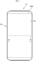
- FIG. 1 is a diagram of an organic light-emitting display device according to an embodiment of the present disclosure.
- an organic light-emitting display device 10 may include a display area DA and a non-display area NDA.
- the non-display area DA is defined as an area in which an image is displayed.
- the display area DA may be used to detect an external environment.
- the display area DA may be used to display an image or to recognize a fingerprint of a user.
- the display area DA may be flat, but the present disclosure is not limited thereto.
- the display area DA may be at least partially curved.
- the display area DA may be disposed in an edge area EA of the organic light-emitting display device 10.
- the edge area EA may include upper, lower, left, and right parts of the display area DA.
- the non-display area NDA is disposed on the outside of (e.g., along a periphery of) the display area DA and is defined as an area in which no image is displayed.
- a speaker module, a camera module, a sensor module, and the like may be provided in the non-display area NDA.
- the sensor module may include at least one of an illumination sensor, a proximity sensor, an infrared (IR) sensor, and an ultrasonic sensor.
- FIG. 2 is a cross-sectional view taken along the line I1-I1' of FIG. 1 .
- an organic light-emitting display device 10 may include a display panel 100, an input sensing layer 200, an anti-reflection panel 300, and a window panel 400.
- An element coupled to another element via an adhesive member will hereinafter be referred to as a panel, and an element formed together with another element by a continuous process will hereinafter be referred to as a layer.
- a panel may include a base layer that provides a base surface, whereas a layer has no base layer. That is, a layer refers to an element disposed on a base surface of another element.
- a base layer may be a single-layer film, such as a synthetic resin film or a composite film, or a multilayer film having a stack of a plurality of films.
- the base layer may include a glass substrate.
- the display panel 100 is defined as a panel for displaying an image.
- the display panel 100 includes a plurality of display elements.
- the plurality of display elements may be organic light-emitting diodes (OLEDs).
- the input sensing layer 200 may sense a hand of the user or a touch pen.
- the input sensing layer 200 may be disposed on the display panel 100.
- the input sensing layer 200 may be formed on the display panel 100 by a continuous process.
- the anti-reflection panel 300 may reduce the reflectance of external light incident thereupon from above the window panel 400.
- the anti-reflection panel 300 may be disposed on the input sensing layer 200 and may be coupled to the input sensing layer 200 via a first adhesive member 510.
- the anti-reflection panel 300 may include a retarder and a polarizer.
- the anti-reflection panel 300 may further include a black matrix and color filters.
- the window panel 400 may protect the display panel 100 and/or the input sensing layer 200 from being scratched.
- the window panel 400 may be disposed on the anti-reflection panel 300 and may be coupled to the anti-reflection panel 300 via a second adhesive member 520.
- the first and second adhesive members 510 and 520 may be pressure sensitive adhesives (PSAs), optically clear adhesives (OCAs), or optically clear resins (OCRs).
- PSAs pressure sensitive adhesives
- OCAs optically clear adhesives
- OCRs optically clear resins
- the anti-reflection panel 300 may be an anti-reflection layer, in which case the anti-reflection layer may be formed directly on the input sensing layer 200 without the aid of an additional adhesive member (e.g., when the anti-reflection layer is used in place of the anti-reflection panel 300, the first adhesive member 510 may be omitted).
- the planar structure of the input sensing layer 200 will hereinafter be described with reference to FIG. 3 .
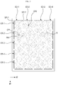
- FIG. 3 illustrates the planar shape of the input sensing layer 200 shown in FIG. 2 .
- the input sensing layer 200 may include a plurality of first sensing electrodes IE1-1 through IE1-5 and a plurality of second sensing electrodes IE2-1 through IE2-4.
- the first sensing electrodes IE1-1 through IE1-5 may extend in a first direction d1.
- the second sensing electrodes IE2-1 through IE2-4 may extend in a second direction d2.
- the first direction d1 may cross the second direction d2.
- the first direction d1 may be a column direction
- the second direction d2 may be a row direction.
- each of the first sensing electrodes IE1-1 through IE1-5 may include (e.g., may be connected to) a plurality of first sensing lines SPL1, which are disposed to form a mesh shape. Areas PA1 defined by the first sensing lines SPL1 (e.g., defined by openings in the mesh shape of the first sensing lines SPL1) may overlap with organic light-emitting layers 150 shown in FIG. 6 , which will be further described later. As used herein, the expression “first and second elements overlapping with each other" or “first and second elements overlap each other” means that the first and second elements overlap each other in a vertical direction with respect to a substrate 110 shown in FIG. 6 .
- the input sensing layer 200 may further include a plurality of first connecting portions CP1, which electrically connect adjacent ones of the first sensing lines SPL1 to one another.
- Each of the second sensing electrodes IE2-1 through IE2-4 may include a plurality of second sensing lines SPL2, which are disposed to form a mesh shape. Areas PA2 defined by the second sensing lines SPL2 (e.g., defined by openings in the mesh shape of the second sensing lines SPL2), like the areas PA1 defined by the first sensing lines SPL1, may overlap the organic light-emitting layers 150 shown in FIG. 6 .
- the input sensing layer 200 may further include a plurality of second connecting portions CP2, which electrically connect adjacent ones of the second sensing lines SPL2 to one another.
- the areas PA1 defined by the first sensing lines SPL1 and the areas PA2 defined by the second sensing lines SPL2 may have a rhombus shape.
- rhombus shape includes not only a substantially perfect rhomboid shape but also includes an almost or substantially rhomboid shape in consideration of processing conditions and the arrangement of the first sensing lines SPL1 and/or the second sensing lines SPL2.
- the areas PA1 defined by the first sensing lines SPL1 are electrically insulated from the areas PA2 defined by the second sensing lines SPL2.
- the first sensing lines SPL1 and the second sensing lines SPL2 may be disposed on the same layer, in which case, the first connecting portions CP1 may be disposed on a different layer than the second connecting portions CP2 and may be electrically insulated from the second connecting portions CP2.
- the first sensing lines SPL1 may be disposed on a different layer from the second sensing lines SPL2.
- the first sensing lines SPL1 and the second sensing lines SPL2 may include a conductive material.
- the conductive material may be a low-resistance metal, such as silver (Ag), aluminum (Al), chromium (Cr), or nickel (Ni), or a conductive nanomaterial, such as silver (Ag) nanowires or carbon nanotubes.
- the input sensing layer 200 may further include a signal pad unit, which provides signals to the first sensing electrodes IE1-1 through IE1-5 and the second sensing electrodes IE2-1 through IE2-4, and a plurality of signal lines.
- a signal pad unit which provides signals to the first sensing electrodes IE1-1 through IE1-5 and the second sensing electrodes IE2-1 through IE2-4, and a plurality of signal lines.
- the relationship between the elements of the display panel 100 and the elements of the input sensing layer 200 will hereinafter be further described with reference to FIGS. 4-7 using the area A of FIG. 3 as a reference.
- the first sensing lines SPL1 and the second sensing lines SPL2 will hereinafter be described by using the first sensing lines SPL1 disposed in the area A as an example.
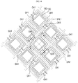
- FIG. 4 is an enlarged plan view of the area A of FIG. 3 .
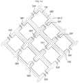
- FIGS. 5A and 5B are plan views showing the layout of elements shown in FIG. 4 .
- FIG. 6 is a cross-sectional view taken along the line I2-I2' of FIG. 4
- FIG. 7 is a cross-sectional view taken along the line I3-I3' of FIG. 4 .
- FIG. 5A illustrates only the first sensing lines SPL1 and a common electrode 160 from among the elements disposed in the area A
- FIG. 5B further illustrates a black matrix BM to the illustration of FIG. 5A
- FIGS. 4-5B illustrate second openings OP2 in the black matrix BM for distinction with other elements.
- the elements of the display panel 100 will hereinafter be described.
- the display panel 100 may include the substrate 110, a via layer 120, a plurality of pixel electrodes 130, a pixel defining film 140, a plurality of organic light-emitting layers 150, a common electrode 160, and an encapsulation layer 170.
- the substrate 110 may be an insulating substrate.
- the substrate 110 may include a material, such as glass, quartz, or a polymer resin.
- the polymer resin may include polyethersulfone (PES), polyacrylate (PA), polyarylate (PAR), polyetherimide (PEI), polyethylene naphthalate (PEN), polyethylene terephthalate (PET), polyphenylene sulfide (PPS), polyarylate, polycarbonate (PC), cellulose triacetate (CAT), cellulose acetate propionate (CAP), or a combination thereof.
- the substrate 110 may be a flexible substrate including polyimide (PI) and/or may have a stack of a plurality of films.
- PI polyimide
- the via layer 120 may be disposed on the substrate 110.
- FIGS. 6 and 7 schematically illustrate the via layer 120 as a layer in which a buffer layer, a plurality of conductive wires, an insulating layer, and a plurality of thin-film transistors (TFTs) are disposed. That is, the via layer 120 may be a stack of a plurality of layers.
- the plurality of thin film transistors may include (or be formed used) amorphous silicon, polysilicon, low-temperature polysilicon (LTPS), an oxide semiconductor, an organic semiconductor, or the like as their channel layer.
- the plurality of TFTs may have different types of channel layers.
- a TFT including an oxide semiconductor and a TFT including LTPS may both be included in a single pixel unit in consideration of the functions of the TFTs or the order of processing.
- the pixel electrodes 130 may be disposed on the via layer 120.
- the pixel electrodes 130 may be anode electrodes.
- the pixel electrodes 130 may be transparent or translucent electrodes or may be formed of a reflective material, such as Al, Ag, Cr, or an alloy thereof.
- the transparent or translucent electrodes may include at least one selected from the group consisting of indium tin oxide (ITO), indium zinc oxide (IZO), zinc oxide (ZnO), indium oxide (In 2 O 3 ), indium gallium oxide (IGO), and aluminum-doped zinc oxide (AZO).
- the reflective material may include at least one selected from the group consisting of Ag, magnesium (Mg), Cr, gold (Au), platinum (Pt), Ni, copper (Cu), tungsten (W), and Al.
- each of the pixel electrodes 130 may be a single film, but the present disclosure is not limited thereto.
- each of the pixel electrodes 130 may be formed as a multilayer film having a stack of two or more materials.
- each of the pixel electrodes 130 may include a reflective film and a transparent or translucent electrode disposed on the reflective film.
- each of the pixel electrodes 130 may include a reflective film and a transparent or translucent electrode disposed below the reflective film.
- the pixel electrodes 130 may have a triple-layer structure of ITO/Ag/ITO, but the present disclosure is not limited thereto.
- the pixel defining film 140 may be disposed on the pixel electrodes 130.
- the pixel defining film 140 may include a plurality of openings, which at least partially expose the pixel electrodes 130.
- the pixel defining film 140 may include an organic material or an inorganic material.
- the pixel defining film 140 may include a material, such as photoresist, a polyimide (PI) resin, an acrylic resin, a silicon compound, or a polyacrylic resin.
- the organic light-emitting layers 150 may be disposed on the pixel electrodes 130 and the pixel defining film 140. In one embodiment, the organic light-emitting layers 150 may at least partially cover the sides of the pixel defining film 140.
- the organic light-emitting layers 150 may emit one of red light, blue light, and green light. In another embodiment, the organic light-emitting layers 150 may emit white light or one of cyan light, magenta light, and yellow light. When the organic light-emitting layers 150 emit white light, the organic light-emitting layers 150 may include a white-light-emitting material or may have a stack including a red-light-emitting layer, a green-light-emitting layer, and a blue-light-emitting layer.
- the organic light-emitting display device 10 may employ a front emission scheme in which light emitted from the organic light-emitting layers 150 is provided in an upward direction (in the example of FIGS. 5A and 5B ). In other embodiments, the organic light-emitting display device 10 may employ a rear emission scheme or a both-side emission scheme (e.g., a top- and bottom-emission scheme).
- the common electrode 160 may be disposed on the organic light-emitting layers 150 and the pixel defining film 140.
- the common electrode 160 may partially overlap the first sensing lines SPL1.
- the regions of overlap between the common electrode 160 and the first sensing lines SPL1 will hereinafter be referred to as overlapping regions OA1, and portions of the common electrode 160 that do not overlap the first sensing lines SPL1 will hereinafter be referred to as open regions OA2.
- the common electrode 160 may be disposed on the organic light-emitting layers 150 and on the pixel defining film 140.
- the common electrode 160 may be a cathode electrode.
- the common electrode 160 may include at least one selected from the group consisting of lithium (Li), calcium (Ca), lithium fluoride/calcium (LiF/Ca), lithium fluoride/aluminum (LiF/Al), Al, Ag, and Mg.
- the common electrode 160 may be formed of a material having a low work function.
- the common electrode 160 may be a transparent or translucent electrode including at least one selected from the group consisting of ITO, IZO, ZnO, In 2 O 3 , IGO, and AZO.
- the pixel electrodes 130, the organic light-emitting layers 150, and the common electrode 160 may form OLEDs.
- the encapsulation layer 170 may be disposed to face the substrate 110 and may cover the OLEDs.
- the encapsulation layer 170 may prevent or reduce the infiltration of moisture and air into the OLEDs.
- the encapsulation layer 170 may be formed as a multilayer film including at least one organic layer and at least one inorganic layer.
- the encapsulation layer 170 may include a first inorganic layer, which is disposed on the common electrode 160, an organic layer, which is disposed on the first inorganic layer, and a second inorganic layer, which is disposed on the organic layer.
- the first and second inorganic layers of the encapsulation layer 170 may include at least one selected from the group consisting of silicon oxide (SiO x ), silicon nitride (SiN x ), and silicon oxynitride (SiON x ).
- the organic layer of the encapsulation layer 170 may include at least one of an acrylic resin, a methacrylic resin, polyisoprene, a vinyl resin, an epoxy resin, a urethane resin, a cellulose resin, a siloxane resin, a PI resin, a polyamide resin, and a perylene resin.
- the encapsulation layer 170 may include a hexamethyldisiloxane (HMDSO) layer.
- HMDSO hexamethyldisiloxane
- the organic layer of the encapsulation layer 170 may be replaced with the HMDSO layer.
- the HMDSO layer may be formed in the same chamber as the first inorganic layer after the formation of the first inorganic layer. In this manner, the formation of the encapsulation layer 170 is simplified.
- the encapsulation layer 170 may be a transparent insulating substrate.
- the transparent insulating substrate may be a glass substrate, a quartz substrate, or a transparent resin substrate.
- the encapsulation layer 170 may be coupled to the substrate 110 via an additional sealing member.
- the black matrix BM may be disposed on the encapsulation layer 170.
- the black matrix BM may be formed of a dark pigment or dye, such as a black pigment or dye, a gray pigment or dye, or a light-shielding material, such as photoresist.
- the black matrix BM may be disposed to overlap the first sensing lines SPL1 and the second sensing lines SPL2.
- the black matrix BM may be formed on the entire encapsulation layer 170 and may have the second openings OP2 therein, which release light emitted by the organic light-emitting layers 150 outwardly (e.g., which allow light emitted by the organic light-emitting layers 150 to pass through the black matrix BM).
- a buffer layer may be further disposed between the black matrix BM and the encapsulation layer 170.
- the black matrix BM may at least partially overlap the common electrode 160 and a plurality of conductive lines. Accordingly, the reflectivity of the organic light-emitting display device 10 is reduced.
- the term "reflectivity” is defined as the ratio of the amount of light reflected by the elements of the organic light-emitting display device 10 that is emitted outwardly to the amount of external light provided to (e.g., incident on) the organic light-emitting display device 10 from the outside of the organic light-emitting display device 10. The relationship between the reflectivity of the organic light-emitting display device 10 and the second openings OP2 in the black matrix BM will be described later with reference to FIGS. 8-10 .
- a planarization layer 180 may be disposed on the black matrix BM to cover the black matrix BM.
- the planarization layer 180 may planarize a height difference formed by the black matrix BM (e.g., formed by the second openings OP2 in the black matrix BM).
- the planarization layer 180 may be an organic layer.
- the planarization layer 180 may include at least one of an acrylic resin, a methacrylic resin, polyisoprene, a vinyl resin, an epoxy resin, a urethane resin, a cellulose rein, a siloxane resin, a PI resin, a polyamide resin, and a perylene resin.
- the first sensing lines SPL1 may be disposed on the planarization layer 180.
- the first sensing lines SPL1 may overlap the black matrix BM and the pixel defining film 140. When the first sensing lines SPL1 completely overlap the black matrix BM, the first sensing lines SPL1 may not be viewable to the user.
- the first sensing lines SPL1 may overlap the common electrode 160 in the overlapping regions OA1, and the first sensing lines SPL1 may not overlap the common electrode 160 in areas other than the overlapping regions OA1, e.g., in the open regions OA2. This will be further described later with reference to FIGS. 8-10 .
- the second sensing lines SPL2 and the first connecting portions CP1 may be further disposed on the planarization layer 180.
- a first insulating layer 210 may be disposed on the first sensing lines SPL1 and the planarization layer 180.
- the first insulating layer 210 may include an inorganic material.
- the inorganic material may include at least one selected from the group consisting of SiO x , SiN x , and SiON x .
- the first insulating layer 210 may include an organic material.
- the organic material may include at least one of an acrylic resin, a methacrylic resin, polyisoprene, a vinyl resin, an epoxy resin, a urethane resin, a cellulose rein, a siloxane resin, a PI resin, a polyamide resin, and a perylene resin.
- a plurality of second connecting portions CP2, which electrically connect adjacent ones of the second sensing lines SPL2 to one another, may be disposed on the first insulating layer 210.
- the location of the first connecting portions CP1 and the location of the second connecting portions CP2 may be switched.
- the second connecting portions CP2 may be disposed on the planarization layer 180
- the first connecting portions CP1 may be disposed on the first insulating layer 210. That is, the location of the first connecting portions CP1 and the location of the second connecting portions CP2 are not particularly limited as long as the first sensing lines SPL1 are electrically connected to one another by the first connecting portions CP1 and the second sensing lines SPL2 are electrically connected to one another by the second connecting portions CP2.
- a second insulating layer 220 may be disposed on the first insulating layer 210.
- the second insulating layer 220 may include an inorganic material or an organic material. Examples of the inorganic material or the organic material that may be used to form the second insulating layer 220 have been described above, and thus, a repeated description thereof is omitted.
- FIGS. 6 and 7 illustrate the first and second insulating layers 210 and 220 as being single layers, but the present disclosure is not limited thereto. In other embodiments, the first and second insulating layers 210 and 220 may each have a multilayer structure.
- the reflectivity and the viewing angle of the organic light-emitting display device 10 and the touch sensitivity of the input sensing layer 200 will hereinafter be described based on a width w1 of the second openings OP2 in the black matrix BM, a height h1 of the encapsulation layer 170 (e.g., a height h1 from a top surface of the pixel defining film 140 to a top surface of the encapsulation layer 170), and the overlapping area ratio between the first sensing lines SPL1 and the common electrode 160.
- the width w1 of the second openings OP2 in the black matrix BM and the reflectivity of the organic light-emitting display device 10 will be described.
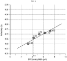
- FIG. 8 is a graph showing the relationship between the reflectivity of an organic light-emitting display device and the width of openings in a black matrix.
- the reflectivity of the organic light-emitting display device 10 increases.
- the reflectivity of the organic light-emitting display device 10 varies depending on the width w1 of the second openings OP2 in the black matrix BM.
- the reflectivity of the organic light-emitting display device 10 can be modified (or controlled) by adjusting the width w1 of the second openings OP2 in the black matrix BM.
- the organic light-emitting display device 10 may be designed to have a reflectivity of about 4.66% or less.
- the second openings OP2 in the black matrix BM may be formed to have a width w1 of about 4.4 ⁇ m or less. If the reflectivity of the organic light-emitting display device 10 is too high, the degree of color separation of reflected light may increase, and as a result, visibility may be degraded. This will hereinafter be described with reference to FIGS. 9A and 9B .
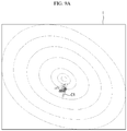
- FIG. 9A shows the distribution of colors of reflected light from an organic light-emitting display device according to a comparative example.
- FIG. 9B shows the distribution of colors of reflected light from the organic light-emitting display device according to an embodiment of the present disclosure.
- FIG. 9A shows a comparative example in which the width of openings in a black matrix is about 7.2 ⁇ m and reflectivity is about 4.73%.
- FIG. 9B shows an embodiment of the present disclosure in which the width w1 of the second openings OP2 in the black matrix BM is about 4.4 ⁇ m and reflectivity is about 4.65%.
- the reflectivity of the organic light-emitting display device 10 is lower than the reflectivity of the organic light-emitting display device according to the comparative example because the width w1 of the second openings OP2 in the black matrix BM is smaller in the organic light-emitting display device 10 than in the organic light-emitting display device according to the comparative example. Because the reflectivity of the organic light-emitting display device according to the comparative example is relatively high, the degree of color separation of light reflected by the organic light-emitting display device according to the comparative example may increase, and as a result, the visibility of the organic light-emitting display device according to the comparative example may be degraded.
- the circles c2 of FIG. 9B are more uniformly distributed in the rectangle t than the circles c1 of FIG. 9A .
- the rectangle t represents color coordinates.
- Each of the circles c1 or c2 represents the color of reflected light at different inclination angles.
- the color of reflected light is uniform, which means that the degree of color separation of reflected light is small.
- the degrees of color separation of reflected light is large.
- the degree of color separation of reflected light from the organic light-emitting display device according to the comparative example is greater than the degree of color separation of reflected light from the organic light-emitting display device 10.
- the degree of color separation of reflected light from the organic light-emitting display device 10 can be reduced as well, and as a result, the visibility of the organic light-emitting display device 10 is improved.
- the reflectivity of the organic light-emitting display device 10 can be reduced to about 4.65% or less.
- the degree of color separation of reflected light from the organic light-emitting display device 10 can be reduced, and the visibility of the organic light-emitting display device 10 is improved.
- the second openings OP2 in the black matrix BM may be formed to have a width w1 of about 3.0 ⁇ m or greater.
- the second openings OP2 in the black matrix BM are emission areas where light is emitted outwardly from the organic light-emitting layers 150.
- the second openings OP2 in the black matrix BM may be formed to have a width w1 of about 3.0 ⁇ m or greater, sufficient emission areas can be secured.
- the width w1 of the second openings OP2 may be in a range of about 3.0 ⁇ m to about 4.4 ⁇ m. Accordingly, the organic light-emitting display device 10 may have a reflectivity of about 4.6% to about 4.65%. As the width w1 of the second openings OP2 in the black matrix BM decreases, the viewing angel of the organic light-emitting display device 10 also decreases.
- FIGS. 10A and 10B are cross-sectional views for explaining the relationship between the viewing angle of an organic light-emitting display device and the height of an encapsulation layer.
- like reference numerals indicate like elements.
- a viewing angle may be defined as the angle between an imaginary line I1 connecting one side of an organic light-emitting layer 150 and one side of a black matrix BM and an imaginary line I2 extending vertically from a substrate 110.
- the organic light-emitting display device shown in FIG. 10A differs from the organic light-emitting display device shown in FIG. 10B in the height of an encapsulation layer 170' or 170". Specifically, a height h' of the encapsulation layer 170' shown in FIG. 10A is greater than a height h" of the encapsulation layer 170" shown in FIG. 10B . However, a width w1 of second openings OP2 in the black matrix BM is the same in both of the organic light-emitting display devices shown in FIGS. 10A and 10B .
- a viewing angle va1 of the organic light-emitting display device shown in FIG. 10A may be smaller than a viewing angle va2 of the organic light-emitting display device shown in FIG. 10B because the height h' of the encapsulation layer 170' shown in FIG. 10A is greater than the height h" of the encapsulation layer 170" shown in FIG. 10B .
- the viewing angle of the organic light-emitting display device 10 can be increased by reducing the height h1 of the encapsulation layer 170 shown in FIG. 6 in a given condition regarding the width w1 of the second openings OP2 in the black matrix BM (e.g., when the width w1 of the second openings OP2 in the black matrix BM remains constant).
- the viewing angle of the organic light-emitting display device 10 can be modified (or controlled) by adjusting the height h1 of the encapsulation layer 170 in the above-described reflectivity condition.
- the organic light-emitting display device 10 may be formed to have a viewing angle of 45°.
- the organic light-emitting display device 10 will hereinafter be described as having a viewing angle of, for example, 45° (even though, in practice, the viewing angle may slightly vary from 45° due to manufacturing tolerances and the like).
- the height of the encapsulation layer 170 is defined as the distance from the top surface of the pixel defining film 140 to the top surface of the encapsulation layer 170.
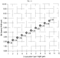
- FIG. 11 is a graph showing the relationship between the width of openings in a black matrix and the height of an encapsulation layer when the viewing angle of an organic light-emitting display device is 45°.
- the viewing angle of the organic light-emitting display device 10 can be modified (or controlled) by adjusting the width w1 of the second openings OP2 in the black matrix BM and the height h1 of the encapsulation layer 170.
- the organic light-emitting display device 10 may be formed to have a viewing angle of about 45° when the height h1 of the encapsulation layer 170 is reduced in accordance with the decrease of the width w1 of the second openings OP2 in the black matrix BM.
- the second openings OP2 in the black matrix BM may be formed to have a width w1 of about 3.0 ⁇ m to about 4.4 ⁇ m in consideration of a reflectivity condition.
- the organic light-emitting display device 10 may be formed to have a viewing angle of about 45°.
- the touch sensitivity of the input sensing layer 200 will hereinafter be described based on the height h1 of the encapsulation layer 170 and the overlapping area ratio between the first sensing lines SPL1 and the common electrode 160.
- the first sensing lines SPL1 are used as a reference, but the following description may also be applicable to the second sensing lines SPL2.
- the viewing angle of the organic light-emitting display device 10 may be increased.
- a distance h2 between the input sensing layer 200 (e.g., the first sensing lines SPL1) and the common electrode 160 decreases.
- the influence of the common electrode 160 on the first sensing lines SPL1 considerably increases (e.g., increases exponentially).
- the touch sensitivity of the input sensing layer 200 may be reduced.
- the overlapping area of the first sensing lines SPL1 and the common electrode 160 may be reduced by removing portions of the common electrode 160 (e.g., by forming the common electrode 160 to have open areas). In this manner, the touch sensitivity of the input sensing layer 200 may not be reduced or substantially reduced due to the influence of the common electrode 160.
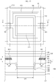
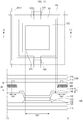
- FIG. 12 shows a plan view of the area B of FIG. 4 and a cross-sectional view taken along the line 111-111' of FIG. 12 .
- FIG. 13 shows a plan view of the area B of FIG. 4 and a cross-sectional view taken along the line II2-II2' of FIG. 13 .
- FIG. 14 is a table showing relative static capacitance values for different encapsulation layer heights and for different overlapping area ratios.
- each rectangular area defined by the first sensing lines SPL1 will hereinafter be referred to as a pixel region PG, and four sides of the pixel region PG may substantially coincide with the sides of the first sensing lines SPL1 that define the pixel region PG.
- the pixel region PG illustrated in FIG. 12 and the pixel region PG illustrated in FIG. 13 are the same except for the direction in which they are arranged in a plan view.
- values less than 100% indicate an improved touch sensitivity with small static capacitance, and a value greater than 100% indicate a degraded touch sensitivity because of high static capacitance.
- the area of the overlapping regions OA1 may be represented by the overlapping area ratio between first sensing lines SPL1 disposed in a pixel region PG and the common electrode 160. That is, the overlapping area ratio between the first sensing lines SPL1 and the common electrode 160 may be defined as the ratio by which first sensing lines SPL1 (or second sensing lines SPL2) disposed in each pixel region PG overlap the common electrode 160. For example, the overlapping area ratio between the first sensing lines SPL1 and the common electrode 160 may be 100% when the first sensing lines SPL1 completely overlap the common electrode 160 in each pixel region PG. On the other hand, the overlapping area ratio between the first sensing lines SPL1 and the common electrode 160 may be 0% when the first sensing lines SPL1 do not overlap the common electrode 160 in each pixel region PG.
- the common electrode 160 may not be arranged in an island-like manner. Also, because a common voltage is applied to the common electrode 160, resistance may not be considered. Accordingly, the overlapping area ratio between the first sensing lines SPL1 and the common electrode 160 can be set to about 2.5% or greater.
- the encapsulation layer 170 may be formed to have a height h1 of about 3.4 ⁇ m to about 6.2 ⁇ m in consideration of the width w1 of the second openings OP2 in the black matrix BM and the viewing angle of the organic light-emitting display device 10.
- the overlapping area ratio between the first sensing lines SPL1 and the common electrode 160 may be set to about 2.5% to about 77.5% in consideration of conditions regarding the height h1 of the encapsulation layer 170 and a minimum overlapping area ratio. For example, when the height h1 of the encapsulation layer 170 is about 3.4 ⁇ m, the overlapping area ratio between the first sensing lines SPL1 and the common electrode 160 may be set to about 2.5% to about 42.5%. Also, when the height h1 of the encapsulation layer 170 is about 6.2 ⁇ m, the overlapping area ratio between the first sensing lines SPL1 and the common electrode 160 may be set to about 2.5% to about 77.5%.
- the overlapping area ratio between the first sensing lines SPL1 and the common electrode 160 has been described above using a single pixel region PG as a reference, but the overlapping area ratio may be set to about 2.5% to about 77.5% in all of the pixel regions PG.
- the common electrode 160 may be formed by a fine metal mask (FMM) process.
- two overlapping regions OA1 are provided in one pixel region PG, but the present disclosure is not limited thereto. This will hereinafter be described with reference to FIG. 15 .
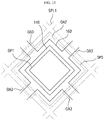
- FIG. 15 is a plan view illustrating a pixel region of an organic light-emitting display device according to another embodiment of the present disclosure.
- the number of overlapping regions OA3 between a plurality of first sensing lines SPL1 and a common electrode 160' is not particularly limited.
- four overlapping regions OA3 may be provided between the first sensing lines SPL1 and the common electrode 160' in one pixel region PG.
- the locations, the number, and the shape of the overlapping regions OA3 are not particularly limited as long as the overlapping area ratio between the first sensing lines SPL1 and the common electrode 160' falls within the range of about 2.5% to about 77.5%.
Landscapes
- Engineering & Computer Science (AREA)
- General Engineering & Computer Science (AREA)
- Theoretical Computer Science (AREA)
- Physics & Mathematics (AREA)
- Microelectronics & Electronic Packaging (AREA)
- Human Computer Interaction (AREA)
- General Physics & Mathematics (AREA)
- Optics & Photonics (AREA)
- Geometry (AREA)
- Electroluminescent Light Sources (AREA)
- Devices For Indicating Variable Information By Combining Individual Elements (AREA)
Abstract
Description
- Aspects of embodiments of the present invention relate to an organic light-emitting display device.
- Display devices have become increasingly important following developments in multimedia technology. Accordingly, various types of display devices, such as a liquid crystal display (LCD) device, an organic light-emitting display device, etc., have been developed.
- The organic light-emitting display device displays an image using organic light-emitting diodes (OLEDs), which generate light through the recombination of electrons and holes. The organic light-emitting display device has various features, such as fast response speed, high luminance, wide viewing angle, and low power consumption.
- Embodiments of the present invention seek to provide an organic light-emitting display device having reducing reflectivity by modifying the width of openings in a black matrix.
- Embodiments of the present invention also set out to provide an organic light-emitting display device having a viewing angle of about 45° by modifying the height of an encapsulation layer in consideration of a reflectivity condition.
- Embodiments of the present invention also seek to provide an organic light-emitting display device that prevents or substantially mitigates a decrease in touch sensitivity by controlling the overlapping area ratio between a common electrode and an input sensing layer in consideration of reflectivity and viewing angle conditions.
- However, embodiments of the present invention are not restricted or limited to the above-described aspects and features, nor is the present invention limited to the embodiments set forth herein. Aspects and features of the present invention will become more apparent to one of ordinary skill in the art to which the present disclosure pertains by referencing the detailed description given below.
- According to an embodiment of the present disclosure, an organic light-emitting display device includes: a substrate; a pixel electrode on the substrate; a pixel defining film on the pixel electrode and having a first opening at least partially exposing the pixel electrode; an organic light-emitting layer on the exposed portion of the pixel electrode; a common electrode on the organic light-emitting layer and the pixel defining film; an encapsulation layer on the common electrode; a black matrix on the encapsulation layer and having a second opening overlapping the first opening; and a plurality of first sensing lines on the black matrix and surrounding the pixel electrode in a plan view to define a pixel region. At least portions of the first sensing lines defining the pixel region do not overlap the common electrode in the pixel region.
- According to an embodiment of the present disclosure, an organic light-emitting display device includes a display panel for displaying an image and an input sensing layer on the display panel. The display panel includes: a substrate; a pixel electrode on the substrate; a pixel defining film having a first opening at least partially exposing the pixel electrode; a common electrode on the pixel defining film; an encapsulation layer on the common electrode; and a black matrix on the encapsulation layer and having a second opening overlapping the first opening. The input sensing layer includes a plurality of first sensing lines surrounding the pixel electrode in a plan view. The first sensing lines have first regions that overlap the common electrode and second regions that do not overlap the common electrode.
- At least some of the above features that accord with the invention, and other features according to the invention, are set out in the claims.
- According to the aforementioned and other embodiments of the present disclosure, reflectivity can be reduced by controlling the width of openings of a black matrix.
- Also, a viewing angle can be improved by controlling the height of an encapsulation layer in consideration of a reflectivity condition.
- Also, the decrease of touch sensitivity can be reduced or prevented by controlling the overlapping area ratio between a common electrode and an input sensing layer in consideration of reflectivity and viewing angle conditions.
- Other features and embodiments may be apparent from the following detailed description, the drawings, and the claims.
- The above and other aspects and features of the present invention will be made more apparent by describing, in detail, embodiments thereof with reference to the attached drawings, in which:
-
FIG. 1 is an organic light-emitting display device according to an embodiment of the present disclosure; -
FIG. 2 is a cross-sectional view taken along the line I1-I1' ofFIG. 1 ; -
FIG. 3 is a plan view of an input sensing layer ofFIG. 2 ; -
FIG. 4 is an enlarged plan view of the area A ofFIG. 3 ; -
FIGS. 5A and5B are plan views showing the layout of elements shown inFIG. 4 ; -
FIG. 6 is a cross-sectional view taken along the line 12-12' ofFIG. 4 ; -
FIG. 7 is a cross-sectional view taken along the line I3-I3' ofFIG. 4 ; -
FIG. 8 is a graph showing the relationship between the reflectivity of an organic light-emitting display device and the width of openings in a black matrix; -
FIG. 9A is a graph showing the distribution of colors of light reflected from an organic light-emitting display device according to a comparative example; -
FIG. 9B is a graph showing the distribution of colors of light reflected from the organic light-emitting display device according to an embodiment of the present disclosure; -
FIGS. 10A and10B are cross-sectional views describing the relationship between the viewing angle of an organic light-emitting display device and the height of an encapsulation layer; -
FIG. 11 is a graph showing the relationship between the width of openings in a black matrix and the height of an encapsulation layer when the viewing angle of an organic light-emitting display device is 45°; -
FIG. 12 shows a plan view of the area B ofFIG. 4 and a cross-sectional view taken along the line 111-111' ofFIG. 12 ; -
FIG. 13 shows a plan view of the area B ofFIG. 4 and a cross-sectional view taken along the line II2-II2' ofFIG. 13 ; -
FIG. 14 is a table showing relative static capacitance values for different encapsulation layer heights and for different overlapping area ratios; and -
FIG. 15 is a plan view illustrating a pixel region of an organic light-emitting display device according to another embodiment of the present disclosure. - In the following description, for the purposes of explanation, various details are set forth to provide a thorough understanding of various embodiments. It will be apparent, however, that various embodiments may be practiced without these specific details or with one or more equivalent arrangements. In other instances, well-known structures and devices are shown in block diagram form in order to avoid unnecessarily obscuring aspects and features of various embodiments.
- In the accompanying figures, sizes and relative sizes of layers, films, panels, regions, etc. may be exaggerated for clarity and descriptive purposes. Also, like reference numerals denote like elements. Further, the use of "may" when describing embodiments of the present invention relates to "one or more embodiments of the present invention."
- When an element or layer is referred to as being "on," "connected to," or "coupled to" another element or layer, it may be directly on, connected to, or coupled to the other element or layer or intervening elements or layers may be present. When an element or layer is referred to as being "directly on," "directly connected to," or "directly coupled to" another element or layer, there are no intervening elements or layers present. For the purposes of this disclosure, "at least one of X, Y, and Z" and "at least one selected from the group consisting of X, Y, and Z" may be construed as only X, only Y, only Z, or any combination of two or more of X, Y, and Z, such as, for instance, XYZ, XYY, YZ, and ZZ. As used herein, the term "and/or" includes any and all combinations of one or more of the associated listed items.
- Although the terms first, second, etc. may be used herein to describe various elements, components, regions, layers, and/or sections, these elements, components, regions, layers, and/or sections should not be limited by these terms. These terms are used to distinguish one element, component, region, layer, and/or section from another element, component, region, layer, and/or section. Thus, a first element, component, region, layer, and/or section discussed below could be termed a second element, component, region, layer, and/or section without departing from the teachings of the present disclosure.
- Spatially relative terms, such as "beneath," "below," "lower," "above," "upper," and the like, may be used herein for descriptive purposes, and, for example, to describe one element or feature's relationship to other element(s) or feature(s) as illustrated in the drawings. Spatially relative terms are intended to encompass different orientations of an apparatus in use, operation, and/or manufacture in addition to the orientation depicted in the drawings. For example, if the apparatus in the drawings is turned over, elements described as "below" or "beneath" other elements or features would then be oriented "above" the other elements or features. Thus, the term "below" can encompass both an orientation of above and below. Furthermore, the apparatus may be otherwise oriented (e.g., rotated 90 degrees or at other orientations), and as such, the spatially relative descriptors used herein should be interpreted accordingly.
- The terminology used herein is for the purpose of describing particular embodiments and is not intended to be limiting. As used herein, the singular forms, "a" and "an" are intended to include the plural forms as well, unless the context clearly indicates otherwise. Moreover, the terms "comprises," "comprising," "includes," and/or "including," when used in this specification, specify the presence of stated features, integers, steps, operations, elements, components, and/or groups thereof but do not preclude the presence or addition of one or more other features, integers, steps, operations, elements, components, and/or groups thereof.
- Various embodiments are described herein with reference to sectional illustrations that are schematic illustrations of idealized embodiments and/or intermediate structures. As such, variations from the shapes of the illustrations due to, for example, manufacturing techniques and/or tolerances, are to be expected. Thus, embodiments disclosed herein should not be construed as limited to the particular illustrated shapes of regions, but are to include deviations in shapes that result from, for instance, manufacturing. For example, a region or area illustrated as a rectangle will, typically, have rounded or curved edges. Thus, the regions and areas illustrated in the drawings are schematic in nature, and their shapes are not intended to illustrate the actual shape of a region of a device and are not intended to be limiting.
- Any numerical range disclosed and/or recited herein is intended to include all sub-ranges of the same numerical precision subsumed within the recited range. For example, a range of "1.0 to 10.0" is intended to include all subranges between (and including) the recited minimum value of 1.0 and the recited maximum value of 10.0, that is, having a minimum value equal to or greater than 1.0 and a maximum value equal to or less than 10.0, such as, for example, 2.4 to 7.6. Any maximum numerical limitation recited herein is intended to include all lower numerical limitations subsumed therein, and any minimum numerical limitation recited in this specification is intended to include all higher numerical limitations subsumed therein.
- Unless otherwise defined, all terms (including technical and scientific terms) used herein have the same meaning as commonly understood by one of ordinary skill in the art to which this disclosure is a part. Terms, such as those defined in commonly used dictionaries, should be interpreted as having a meaning that is consistent with their meaning in the context of the relevant art and should not be interpreted in an idealized or overly formal sense, unless expressly so defined herein.
- Hereinafter, embodiments will be described with reference to the accompanying drawings.
-
FIG. 1 is a diagram of an organic light-emitting display device according to an embodiment of the present disclosure. - Referring to
FIG. 1 , an organic light-emittingdisplay device 10 may include a display area DA and a non-display area NDA. - The non-display area DA is defined as an area in which an image is displayed. The display area DA may be used to detect an external environment. For example, the display area DA may be used to display an image or to recognize a fingerprint of a user. In one embodiment, the display area DA may be flat, but the present disclosure is not limited thereto. In other embodiments, the display area DA may be at least partially curved. The display area DA may be disposed in an edge area EA of the organic light-emitting
display device 10. The edge area EA may include upper, lower, left, and right parts of the display area DA. - The non-display area NDA is disposed on the outside of (e.g., along a periphery of) the display area DA and is defined as an area in which no image is displayed. In one embodiment, a speaker module, a camera module, a sensor module, and the like may be provided in the non-display area NDA. In one embodiment, the sensor module may include at least one of an illumination sensor, a proximity sensor, an infrared (IR) sensor, and an ultrasonic sensor.
-
FIG. 2 is a cross-sectional view taken along the line I1-I1' ofFIG. 1 . - Referring to
FIG. 2 , an organic light-emittingdisplay device 10 may include adisplay panel 100, aninput sensing layer 200, ananti-reflection panel 300, and awindow panel 400. An element coupled to another element via an adhesive member will hereinafter be referred to as a panel, and an element formed together with another element by a continuous process will hereinafter be referred to as a layer. A panel may include a base layer that provides a base surface, whereas a layer has no base layer. That is, a layer refers to an element disposed on a base surface of another element. In one embodiment, a base layer may be a single-layer film, such as a synthetic resin film or a composite film, or a multilayer film having a stack of a plurality of films. The base layer may include a glass substrate. - The
display panel 100 is defined as a panel for displaying an image. Thedisplay panel 100 includes a plurality of display elements. The plurality of display elements may be organic light-emitting diodes (OLEDs). - In one embodiment, the
input sensing layer 200 may sense a hand of the user or a touch pen. Theinput sensing layer 200 may be disposed on thedisplay panel 100. Theinput sensing layer 200 may be formed on thedisplay panel 100 by a continuous process. - The
anti-reflection panel 300 may reduce the reflectance of external light incident thereupon from above thewindow panel 400. Theanti-reflection panel 300 may be disposed on theinput sensing layer 200 and may be coupled to theinput sensing layer 200 via a firstadhesive member 510. In one embodiment, theanti-reflection panel 300 may include a retarder and a polarizer. Theanti-reflection panel 300 may further include a black matrix and color filters. - The
window panel 400 may protect thedisplay panel 100 and/or theinput sensing layer 200 from being scratched. Thewindow panel 400 may be disposed on theanti-reflection panel 300 and may be coupled to theanti-reflection panel 300 via a secondadhesive member 520. - The first and second
adhesive members - In another embodiment different from that which is shown in
FIG. 2 , theanti-reflection panel 300 may be an anti-reflection layer, in which case the anti-reflection layer may be formed directly on theinput sensing layer 200 without the aid of an additional adhesive member (e.g., when the anti-reflection layer is used in place of theanti-reflection panel 300, the firstadhesive member 510 may be omitted). - The planar structure of the
input sensing layer 200 will hereinafter be described with reference toFIG. 3 . -
FIG. 3 illustrates the planar shape of theinput sensing layer 200 shown inFIG. 2 . - Referring to
FIG. 3 , theinput sensing layer 200 may include a plurality of first sensing electrodes IE1-1 through IE1-5 and a plurality of second sensing electrodes IE2-1 through IE2-4. The first sensing electrodes IE1-1 through IE1-5 may extend in a first direction d1. The second sensing electrodes IE2-1 through IE2-4 may extend in a second direction d2. In one embodiment, the first direction d1 may cross the second direction d2. In the example embodiment shown inFIG. 3 , the first direction d1 may be a column direction, and the second direction d2 may be a row direction. - For example, each of the first sensing electrodes IE1-1 through IE1-5 may include (e.g., may be connected to) a plurality of first sensing lines SPL1, which are disposed to form a mesh shape. Areas PA1 defined by the first sensing lines SPL1 (e.g., defined by openings in the mesh shape of the first sensing lines SPL1) may overlap with organic light-emitting
layers 150 shown inFIG. 6 , which will be further described later. As used herein, the expression "first and second elements overlapping with each other" or "first and second elements overlap each other" means that the first and second elements overlap each other in a vertical direction with respect to asubstrate 110 shown inFIG. 6 . Theinput sensing layer 200 may further include a plurality of first connecting portions CP1, which electrically connect adjacent ones of the first sensing lines SPL1 to one another. - Each of the second sensing electrodes IE2-1 through IE2-4 may include a plurality of second sensing lines SPL2, which are disposed to form a mesh shape. Areas PA2 defined by the second sensing lines SPL2 (e.g., defined by openings in the mesh shape of the second sensing lines SPL2), like the areas PA1 defined by the first sensing lines SPL1, may overlap the organic light-emitting
layers 150 shown inFIG. 6 . Theinput sensing layer 200 may further include a plurality of second connecting portions CP2, which electrically connect adjacent ones of the second sensing lines SPL2 to one another. - In one embodiment, the areas PA1 defined by the first sensing lines SPL1 and the areas PA2 defined by the second sensing lines SPL2 may have a rhombus shape. As used herein, the term "rhombus shape" includes not only a substantially perfect rhomboid shape but also includes an almost or substantially rhomboid shape in consideration of processing conditions and the arrangement of the first sensing lines SPL1 and/or the second sensing lines SPL2.
- The areas PA1 defined by the first sensing lines SPL1 are electrically insulated from the areas PA2 defined by the second sensing lines SPL2. In one embodiment, the first sensing lines SPL1 and the second sensing lines SPL2 may be disposed on the same layer, in which case, the first connecting portions CP1 may be disposed on a different layer than the second connecting portions CP2 and may be electrically insulated from the second connecting portions CP2. In another embodiment, the first sensing lines SPL1 may be disposed on a different layer from the second sensing lines SPL2.
- The first sensing lines SPL1 and the second sensing lines SPL2 may include a conductive material. In one embodiment, the conductive material may be a low-resistance metal, such as silver (Ag), aluminum (Al), chromium (Cr), or nickel (Ni), or a conductive nanomaterial, such as silver (Ag) nanowires or carbon nanotubes.
- The
input sensing layer 200 may further include a signal pad unit, which provides signals to the first sensing electrodes IE1-1 through IE1-5 and the second sensing electrodes IE2-1 through IE2-4, and a plurality of signal lines. - The relationship between the elements of the
display panel 100 and the elements of theinput sensing layer 200 will hereinafter be further described with reference toFIGS. 4-7 using the area A ofFIG. 3 as a reference. For convenience, the first sensing lines SPL1 and the second sensing lines SPL2 will hereinafter be described by using the first sensing lines SPL1 disposed in the area A as an example. -
FIG. 4 is an enlarged plan view of the area A ofFIG. 3 .FIGS. 5A and5B are plan views showing the layout of elements shown inFIG. 4 .FIG. 6 is a cross-sectional view taken along the line I2-I2' ofFIG. 4 , andFIG. 7 is a cross-sectional view taken along the line I3-I3' ofFIG. 4 . -
FIG. 5A illustrates only the first sensing lines SPL1 and acommon electrode 160 from among the elements disposed in the area A, andFIG. 5B further illustrates a black matrix BM to the illustration ofFIG. 5A .FIGS. 4-5B illustrate second openings OP2 in the black matrix BM for distinction with other elements. - The elements of the
display panel 100 will hereinafter be described. - The
display panel 100 may include thesubstrate 110, a vialayer 120, a plurality ofpixel electrodes 130, apixel defining film 140, a plurality of organic light-emittinglayers 150, acommon electrode 160, and anencapsulation layer 170. - The
substrate 110 may be an insulating substrate. In one embodiment, thesubstrate 110 may include a material, such as glass, quartz, or a polymer resin. The polymer resin may include polyethersulfone (PES), polyacrylate (PA), polyarylate (PAR), polyetherimide (PEI), polyethylene naphthalate (PEN), polyethylene terephthalate (PET), polyphenylene sulfide (PPS), polyarylate, polycarbonate (PC), cellulose triacetate (CAT), cellulose acetate propionate (CAP), or a combination thereof. - In another embodiment, the
substrate 110 may be a flexible substrate including polyimide (PI) and/or may have a stack of a plurality of films. - The via
layer 120 may be disposed on thesubstrate 110.FIGS. 6 and7 schematically illustrate the vialayer 120 as a layer in which a buffer layer, a plurality of conductive wires, an insulating layer, and a plurality of thin-film transistors (TFTs) are disposed. That is, the vialayer 120 may be a stack of a plurality of layers. - The plurality of thin film transistors (TFTs) may include (or be formed used) amorphous silicon, polysilicon, low-temperature polysilicon (LTPS), an oxide semiconductor, an organic semiconductor, or the like as their channel layer. The plurality of TFTs may have different types of channel layers. In one embodiment, a TFT including an oxide semiconductor and a TFT including LTPS may both be included in a single pixel unit in consideration of the functions of the TFTs or the order of processing.
- The
pixel electrodes 130 may be disposed on the vialayer 120. In one embodiment, thepixel electrodes 130 may be anode electrodes. When thepixel electrodes 130 are anode electrodes, thepixel electrodes 130 may be transparent or translucent electrodes or may be formed of a reflective material, such as Al, Ag, Cr, or an alloy thereof. The transparent or translucent electrodes may include at least one selected from the group consisting of indium tin oxide (ITO), indium zinc oxide (IZO), zinc oxide (ZnO), indium oxide (In2O3), indium gallium oxide (IGO), and aluminum-doped zinc oxide (AZO). The reflective material may include at least one selected from the group consisting of Ag, magnesium (Mg), Cr, gold (Au), platinum (Pt), Ni, copper (Cu), tungsten (W), and Al. - In one embodiment, each of the
pixel electrodes 130 may be a single film, but the present disclosure is not limited thereto. For example, each of thepixel electrodes 130 may be formed as a multilayer film having a stack of two or more materials. - When the
pixel electrodes 130 are formed as multilayer films, each of thepixel electrodes 130 may include a reflective film and a transparent or translucent electrode disposed on the reflective film. In another embodiment, each of thepixel electrodes 130 may include a reflective film and a transparent or translucent electrode disposed below the reflective film. For example, thepixel electrodes 130 may have a triple-layer structure of ITO/Ag/ITO, but the present disclosure is not limited thereto. - The
pixel defining film 140 may be disposed on thepixel electrodes 130. Thepixel defining film 140 may include a plurality of openings, which at least partially expose thepixel electrodes 130. Thepixel defining film 140 may include an organic material or an inorganic material. In one embodiment, thepixel defining film 140 may include a material, such as photoresist, a polyimide (PI) resin, an acrylic resin, a silicon compound, or a polyacrylic resin. - The organic light-emitting
layers 150 may be disposed on thepixel electrodes 130 and thepixel defining film 140. In one embodiment, the organic light-emittinglayers 150 may at least partially cover the sides of thepixel defining film 140. - In one embodiment, the organic light-emitting
layers 150 may emit one of red light, blue light, and green light. In another embodiment, the organic light-emittinglayers 150 may emit white light or one of cyan light, magenta light, and yellow light. When the organic light-emittinglayers 150 emit white light, the organic light-emittinglayers 150 may include a white-light-emitting material or may have a stack including a red-light-emitting layer, a green-light-emitting layer, and a blue-light-emitting layer. The organic light-emittingdisplay device 10 may employ a front emission scheme in which light emitted from the organic light-emittinglayers 150 is provided in an upward direction (in the example ofFIGS. 5A and5B ). In other embodiments, the organic light-emittingdisplay device 10 may employ a rear emission scheme or a both-side emission scheme (e.g., a top- and bottom-emission scheme). - The
common electrode 160 may be disposed on the organic light-emittinglayers 150 and thepixel defining film 140. Thecommon electrode 160 may partially overlap the first sensing lines SPL1. The regions of overlap between thecommon electrode 160 and the first sensing lines SPL1 will hereinafter be referred to as overlapping regions OA1, and portions of thecommon electrode 160 that do not overlap the first sensing lines SPL1 will hereinafter be referred to as open regions OA2. - The
common electrode 160 may be disposed on the organic light-emittinglayers 150 and on thepixel defining film 140. In one embodiment, thecommon electrode 160 may be a cathode electrode. In one embodiment, thecommon electrode 160 may include at least one selected from the group consisting of lithium (Li), calcium (Ca), lithium fluoride/calcium (LiF/Ca), lithium fluoride/aluminum (LiF/Al), Al, Ag, and Mg. Thecommon electrode 160 may be formed of a material having a low work function. In one embodiment, thecommon electrode 160 may be a transparent or translucent electrode including at least one selected from the group consisting of ITO, IZO, ZnO, In2O3, IGO, and AZO. - The
pixel electrodes 130, the organic light-emittinglayers 150, and thecommon electrode 160 may form OLEDs. - The
encapsulation layer 170 may be disposed to face thesubstrate 110 and may cover the OLEDs. Theencapsulation layer 170 may prevent or reduce the infiltration of moisture and air into the OLEDs. - The
encapsulation layer 170 may be formed as a multilayer film including at least one organic layer and at least one inorganic layer. In one embodiment, theencapsulation layer 170 may include a first inorganic layer, which is disposed on thecommon electrode 160, an organic layer, which is disposed on the first inorganic layer, and a second inorganic layer, which is disposed on the organic layer. The first and second inorganic layers of theencapsulation layer 170 may include at least one selected from the group consisting of silicon oxide (SiOx), silicon nitride (SiNx), and silicon oxynitride (SiONx). The organic layer of theencapsulation layer 170 may include at least one of an acrylic resin, a methacrylic resin, polyisoprene, a vinyl resin, an epoxy resin, a urethane resin, a cellulose resin, a siloxane resin, a PI resin, a polyamide resin, and a perylene resin. - In another embodiment, the
encapsulation layer 170 may include a hexamethyldisiloxane (HMDSO) layer. When theencapsulation layer 170 includes the HMDSO layer, the organic layer of theencapsulation layer 170 may be replaced with the HMDSO layer. In one embodiment, the HMDSO layer may be formed in the same chamber as the first inorganic layer after the formation of the first inorganic layer. In this manner, the formation of theencapsulation layer 170 is simplified. - In another embodiment, the
encapsulation layer 170 may be a transparent insulating substrate. The transparent insulating substrate may be a glass substrate, a quartz substrate, or a transparent resin substrate. When theencapsulation layer 170 is a transparent insulating substrate, theencapsulation layer 170 may be coupled to thesubstrate 110 via an additional sealing member. - The black matrix BM may be disposed on the
encapsulation layer 170. The black matrix BM may be formed of a dark pigment or dye, such as a black pigment or dye, a gray pigment or dye, or a light-shielding material, such as photoresist. The black matrix BM may be disposed to overlap the first sensing lines SPL1 and the second sensing lines SPL2. - The black matrix BM may be formed on the
entire encapsulation layer 170 and may have the second openings OP2 therein, which release light emitted by the organic light-emittinglayers 150 outwardly (e.g., which allow light emitted by the organic light-emittinglayers 150 to pass through the black matrix BM). A buffer layer may be further disposed between the black matrix BM and theencapsulation layer 170. - As already mentioned above, because the black matrix BM is formed on the
entire encapsulation layer 170 and includes the second openings OP2, the black matrix BM may at least partially overlap thecommon electrode 160 and a plurality of conductive lines. Accordingly, the reflectivity of the organic light-emittingdisplay device 10 is reduced. As used herein, the term "reflectivity" is defined as the ratio of the amount of light reflected by the elements of the organic light-emittingdisplay device 10 that is emitted outwardly to the amount of external light provided to (e.g., incident on) the organic light-emittingdisplay device 10 from the outside of the organic light-emittingdisplay device 10. The relationship between the reflectivity of the organic light-emittingdisplay device 10 and the second openings OP2 in the black matrix BM will be described later with reference toFIGS. 8-10 . - A
planarization layer 180 may be disposed on the black matrix BM to cover the black matrix BM. Theplanarization layer 180 may planarize a height difference formed by the black matrix BM (e.g., formed by the second openings OP2 in the black matrix BM). In one embodiment, theplanarization layer 180 may be an organic layer. For example, theplanarization layer 180 may include at least one of an acrylic resin, a methacrylic resin, polyisoprene, a vinyl resin, an epoxy resin, a urethane resin, a cellulose rein, a siloxane resin, a PI resin, a polyamide resin, and a perylene resin. - The first sensing lines SPL1 may be disposed on the
planarization layer 180. The first sensing lines SPL1 may overlap the black matrix BM and thepixel defining film 140. When the first sensing lines SPL1 completely overlap the black matrix BM, the first sensing lines SPL1 may not be viewable to the user. - The first sensing lines SPL1 may overlap the
common electrode 160 in the overlapping regions OA1, and the first sensing lines SPL1 may not overlap thecommon electrode 160 in areas other than the overlapping regions OA1, e.g., in the open regions OA2. This will be further described later with reference toFIGS. 8-10 . The second sensing lines SPL2 and the first connecting portions CP1 may be further disposed on theplanarization layer 180. - A first insulating
layer 210 may be disposed on the first sensing lines SPL1 and theplanarization layer 180. In one embodiment, the first insulatinglayer 210 may include an inorganic material. The inorganic material may include at least one selected from the group consisting of SiOx, SiNx, and SiONx. In another embodiment, the first insulatinglayer 210 may include an organic material. The organic material may include at least one of an acrylic resin, a methacrylic resin, polyisoprene, a vinyl resin, an epoxy resin, a urethane resin, a cellulose rein, a siloxane resin, a PI resin, a polyamide resin, and a perylene resin. - A plurality of second connecting portions CP2, which electrically connect adjacent ones of the second sensing lines SPL2 to one another, may be disposed on the first insulating
layer 210. The location of the first connecting portions CP1 and the location of the second connecting portions CP2 may be switched. For example, the second connecting portions CP2 may be disposed on theplanarization layer 180, and the first connecting portions CP1 may be disposed on the first insulatinglayer 210. That is, the location of the first connecting portions CP1 and the location of the second connecting portions CP2 are not particularly limited as long as the first sensing lines SPL1 are electrically connected to one another by the first connecting portions CP1 and the second sensing lines SPL2 are electrically connected to one another by the second connecting portions CP2. - A second insulating
layer 220 may be disposed on the first insulatinglayer 210. In one embodiment, the second insulatinglayer 220 may include an inorganic material or an organic material. Examples of the inorganic material or the organic material that may be used to form the second insulatinglayer 220 have been described above, and thus, a repeated description thereof is omitted.FIGS. 6 and7 illustrate the first and second insulatinglayers layers - The reflectivity and the viewing angle of the organic light-emitting
display device 10 and the touch sensitivity of theinput sensing layer 200 will hereinafter be described based on a width w1 of the second openings OP2 in the black matrix BM, a height h1 of the encapsulation layer 170 (e.g., a height h1 from a top surface of thepixel defining film 140 to a top surface of the encapsulation layer 170), and the overlapping area ratio between the first sensing lines SPL1 and thecommon electrode 160. - First, the width w1 of the second openings OP2 in the black matrix BM and the reflectivity of the organic light-emitting
display device 10 will be described. -
FIG. 8 is a graph showing the relationship between the reflectivity of an organic light-emitting display device and the width of openings in a black matrix. - Referring to
FIG. 8 , as the width w1 of the second openings OP2 in the black matrix BM increases, the reflectivity of the organic light-emittingdisplay device 10 increases. - As shown in
FIG. 8 , the reflectivity of the organic light-emittingdisplay device 10 varies depending on the width w1 of the second openings OP2 in the black matrix BM. In other words, the reflectivity of the organic light-emittingdisplay device 10 can be modified (or controlled) by adjusting the width w1 of the second openings OP2 in the black matrix BM. - The organic light-emitting
display device 10 may be designed to have a reflectivity of about 4.66% or less. To this end, the second openings OP2 in the black matrix BM may be formed to have a width w1 of about 4.4 µm or less. If the reflectivity of the organic light-emittingdisplay device 10 is too high, the degree of color separation of reflected light may increase, and as a result, visibility may be degraded. This will hereinafter be described with reference toFIGS. 9A and9B . -
FIG. 9A shows the distribution of colors of reflected light from an organic light-emitting display device according to a comparative example.FIG. 9B shows the distribution of colors of reflected light from the organic light-emitting display device according to an embodiment of the present disclosure.FIG. 9A shows a comparative example in which the width of openings in a black matrix is about 7.2 µm and reflectivity is about 4.73%. On the other hand,FIG. 9B shows an embodiment of the present disclosure in which the width w1 of the second openings OP2 in the black matrix BM is about 4.4 µm and reflectivity is about 4.65%. That is, as already mentioned above, the reflectivity of the organic light-emittingdisplay device 10 is lower than the reflectivity of the organic light-emitting display device according to the comparative example because the width w1 of the second openings OP2 in the black matrix BM is smaller in the organic light-emittingdisplay device 10 than in the organic light-emitting display device according to the comparative example. Because the reflectivity of the organic light-emitting display device according to the comparative example is relatively high, the degree of color separation of light reflected by the organic light-emitting display device according to the comparative example may increase, and as a result, the visibility of the organic light-emitting display device according to the comparative example may be degraded. - The circles c2 of
FIG. 9B are more uniformly distributed in the rectangle t than the circles c1 ofFIG. 9A . The rectangle t represents color coordinates. Each of the circles c1 or c2 represents the color of reflected light at different inclination angles. When the circles c1 or c2 are uniformly distributed in the rectangle t, the color of reflected light is uniform, which means that the degree of color separation of reflected light is small. On the other hand, when the circles c1 or c2 are widely spread in the rectangle t, the degree of color separation of reflected light is large. - The degree of color separation of reflected light from the organic light-emitting display device according to the comparative example is greater than the degree of color separation of reflected light from the organic light-emitting
display device 10. Thus, by reducing the reflectivity of the organic light-emittingdisplay device 10, the degree of color separation of reflected light from the organic light-emittingdisplay device 10 can be reduced as well, and as a result, the visibility of the organic light-emittingdisplay device 10 is improved. - By forming the second openings OP2 in the black matrix BM to have a width w1 of about 4.4 µm or less, the reflectivity of the organic light-emitting
display device 10 can be reduced to about 4.65% or less. As a result, the degree of color separation of reflected light from the organic light-emittingdisplay device 10 can be reduced, and the visibility of the organic light-emittingdisplay device 10 is improved. - The second openings OP2 in the black matrix BM may be formed to have a width w1 of about 3.0 µm or greater. As already mentioned above, the second openings OP2 in the black matrix BM are emission areas where light is emitted outwardly from the organic light-emitting
layers 150. Thus, by forming the second openings OP2 in the black matrix BM to have a width w1 of about 3.0 µm or greater, sufficient emission areas can be secured. - In short, the width w1 of the second openings OP2 may be in a range of about 3.0 µm to about 4.4 µm. Accordingly, the organic light-emitting
display device 10 may have a reflectivity of about 4.6% to about 4.65%. As the width w1 of the second openings OP2 in the black matrix BM decreases, the viewing angel of the organic light-emittingdisplay device 10 also decreases. - The relationship between the viewing angle of the organic light-emitting
display device 10 and the height h1 of theencapsulation layer 170 in the above-described reflectivity condition will hereinafter be described with reference toFIGS. 4-7 ,10A ,10B , and11 . -
FIGS. 10A and10B are cross-sectional views for explaining the relationship between the viewing angle of an organic light-emitting display device and the height of an encapsulation layer. For convenience, inFIGS. 10A and10B , like reference numerals indicate like elements. - Referring to
FIG. 10A , a viewing angle may be defined as the angle between an imaginary line I1 connecting one side of an organic light-emittinglayer 150 and one side of a black matrix BM and an imaginary line I2 extending vertically from asubstrate 110. - The organic light-emitting display device shown in
FIG. 10A differs from the organic light-emitting display device shown inFIG. 10B in the height of anencapsulation layer 170' or 170". Specifically, a height h' of the encapsulation layer 170' shown inFIG. 10A is greater than a height h" of theencapsulation layer 170" shown inFIG. 10B . However, a width w1 of second openings OP2 in the black matrix BM is the same in both of the organic light-emitting display devices shown inFIGS. 10A and10B . - Even when the width w1 of the second openings OP2 in the black matrix BM is the same in both the organic light-emitting display devices of
FIGS. 10A and10B , a viewing angle va1 of the organic light-emitting display device shown inFIG. 10A may be smaller than a viewing angle va2 of the organic light-emitting display device shown inFIG. 10B because the height h' of the encapsulation layer 170' shown inFIG. 10A is greater than the height h" of theencapsulation layer 170" shown inFIG. 10B . Thus, the viewing angle of the organic light-emittingdisplay device 10 can be increased by reducing the height h1 of theencapsulation layer 170 shown inFIG. 6 in a given condition regarding the width w1 of the second openings OP2 in the black matrix BM (e.g., when the width w1 of the second openings OP2 in the black matrix BM remains constant). - Therefore, the viewing angle of the organic light-emitting
display device 10 can be modified (or controlled) by adjusting the height h1 of theencapsulation layer 170 in the above-described reflectivity condition. In one embodiment, the organic light-emittingdisplay device 10 may be formed to have a viewing angle of 45°. The organic light-emittingdisplay device 10 will hereinafter be described as having a viewing angle of, for example, 45° (even though, in practice, the viewing angle may slightly vary from 45° due to manufacturing tolerances and the like). Referring toFIG. 6 , the height of theencapsulation layer 170 is defined as the distance from the top surface of thepixel defining film 140 to the top surface of theencapsulation layer 170. -
FIG. 11 is a graph showing the relationship between the width of openings in a black matrix and the height of an encapsulation layer when the viewing angle of an organic light-emitting display device is 45°. - Referring to
FIG. 11 , the viewing angle of the organic light-emittingdisplay device 10 can be modified (or controlled) by adjusting the width w1 of the second openings OP2 in the black matrix BM and the height h1 of theencapsulation layer 170. For example, the organic light-emittingdisplay device 10 may be formed to have a viewing angle of about 45° when the height h1 of theencapsulation layer 170 is reduced in accordance with the decrease of the width w1 of the second openings OP2 in the black matrix BM. - As already mentioned above, the second openings OP2 in the black matrix BM may be formed to have a width w1 of about 3.0 µm to about 4.4 µm in consideration of a reflectivity condition. By forming the
encapsulation layer 170 to have a height h1 of about 3.4 µm to about 6.2 µm in consideration of the width w1 of the second openings OP2 in the black matrix BM, the organic light-emittingdisplay device 10 may be formed to have a viewing angle of about 45°. - The touch sensitivity of the
input sensing layer 200 will hereinafter be described based on the height h1 of theencapsulation layer 170 and the overlapping area ratio between the first sensing lines SPL1 and thecommon electrode 160. In the description that follows, the first sensing lines SPL1 are used as a reference, but the following description may also be applicable to the second sensing lines SPL2. - As already mentioned above, when the height h1 of the
encapsulation layer 170 is reduced, the viewing angle of the organic light-emittingdisplay device 10 may be increased. However, referring toFIGS. 7 and12 , as the height h1 of theencapsulation layer 170 decreases, a distance h2 between the input sensing layer 200 (e.g., the first sensing lines SPL1) and thecommon electrode 160 decreases. As the distance h2 between theinput sensing layer 200 and thecommon electrode 160 decreases, the influence of thecommon electrode 160 on the first sensing lines SPL1 considerably increases (e.g., increases exponentially). Thus, the touch sensitivity of theinput sensing layer 200 may be reduced. - In the organic light-emitting
display device 10, the overlapping area of the first sensing lines SPL1 and thecommon electrode 160 may be reduced by removing portions of the common electrode 160 (e.g., by forming thecommon electrode 160 to have open areas). In this manner, the touch sensitivity of theinput sensing layer 200 may not be reduced or substantially reduced due to the influence of thecommon electrode 160. - The overlap of the first sensing lines SPL1 and the
common electrode 160 will hereinafter be described with reference toFIGS. 12-14 . -
FIG. 12 shows a plan view of the area B ofFIG. 4 and a cross-sectional view taken along the line 111-111' ofFIG. 12 .FIG. 13 shows a plan view of the area B ofFIG. 4 and a cross-sectional view taken along the line II2-II2' ofFIG. 13 .FIG. 14 is a table showing relative static capacitance values for different encapsulation layer heights and for different overlapping area ratios. - For convenience, referring to
FIGS. 12 and13 , each rectangular area defined by the first sensing lines SPL1 will hereinafter be referred to as a pixel region PG, and four sides of the pixel region PG may substantially coincide with the sides of the first sensing lines SPL1 that define the pixel region PG. The pixel region PG illustrated inFIG. 12 and the pixel region PG illustrated inFIG. 13 are the same except for the direction in which they are arranged in a plan view. - Referring to
FIG. 14 , values less than 100% indicate an improved touch sensitivity with small static capacitance, and a value greater than 100% indicate a degraded touch sensitivity because of high static capacitance. - As already mentioned above, even when the distance h2 between the
common electrode 160 and the first sensing lines SPL1 is reduced, a decrease of touch sensitivity can be prevented or reduced by reducing the overlapping regions OA1 between thecommon electrode 160 and the first sensing lines SPL1. - The area of the overlapping regions OA1 may be represented by the overlapping area ratio between first sensing lines SPL1 disposed in a pixel region PG and the
common electrode 160. That is, the overlapping area ratio between the first sensing lines SPL1 and thecommon electrode 160 may be defined as the ratio by which first sensing lines SPL1 (or second sensing lines SPL2) disposed in each pixel region PG overlap thecommon electrode 160. For example, the overlapping area ratio between the first sensing lines SPL1 and thecommon electrode 160 may be 100% when the first sensing lines SPL1 completely overlap thecommon electrode 160 in each pixel region PG. On the other hand, the overlapping area ratio between the first sensing lines SPL1 and thecommon electrode 160 may be 0% when the first sensing lines SPL1 do not overlap thecommon electrode 160 in each pixel region PG. - Because portions of the
common electrode 160 need to be electrically connected, thecommon electrode 160 may not be arranged in an island-like manner. Also, because a common voltage is applied to thecommon electrode 160, resistance may not be considered. Accordingly, the overlapping area ratio between the first sensing lines SPL1 and thecommon electrode 160 can be set to about 2.5% or greater. - As already mentioned above, the
encapsulation layer 170 may be formed to have a height h1 of about 3.4 µm to about 6.2 µm in consideration of the width w1 of the second openings OP2 in the black matrix BM and the viewing angle of the organic light-emittingdisplay device 10. - Referring to
FIG. 14 , the overlapping area ratio between the first sensing lines SPL1 and thecommon electrode 160 may be set to about 2.5% to about 77.5% in consideration of conditions regarding the height h1 of theencapsulation layer 170 and a minimum overlapping area ratio. For example, when the height h1 of theencapsulation layer 170 is about 3.4 µm, the overlapping area ratio between the first sensing lines SPL1 and thecommon electrode 160 may be set to about 2.5% to about 42.5%. Also, when the height h1 of theencapsulation layer 170 is about 6.2 µm, the overlapping area ratio between the first sensing lines SPL1 and thecommon electrode 160 may be set to about 2.5% to about 77.5%. - The overlapping area ratio between the first sensing lines SPL1 and the
common electrode 160 has been described above using a single pixel region PG as a reference, but the overlapping area ratio may be set to about 2.5% to about 77.5% in all of the pixel regions PG. - Thus, even when the height h1 of the
encapsulation layer 170 is reduced in consideration of the viewing angle of the organic light-emittingdisplay device 10, a decrease of touch sensitivity can be prevented or reduced by removing at least a portion of thecommon electrode 160 that overlaps with the first sensing lines SPL1. A method to form thecommon electrode 160 is not particularly limited. In one embodiment, thecommon electrode 160 may be formed by a fine metal mask (FMM) process. - In one embodiment, two overlapping regions OA1 are provided in one pixel region PG, but the present disclosure is not limited thereto. This will hereinafter be described with reference to
FIG. 15 . -
FIG. 15 is a plan view illustrating a pixel region of an organic light-emitting display device according to another embodiment of the present disclosure. - Referring to
FIG. 15 , the number of overlapping regions OA3 between a plurality of first sensing lines SPL1 and a common electrode 160' is not particularly limited. For example, four overlapping regions OA3 may be provided between the first sensing lines SPL1 and the common electrode 160' in one pixel region PG. - That is, the locations, the number, and the shape of the overlapping regions OA3 are not particularly limited as long as the overlapping area ratio between the first sensing lines SPL1 and the common electrode 160' falls within the range of about 2.5% to about 77.5%.
Claims (12)
- An organic light-emitting display device comprising:a substrate;a pixel electrode on the substrate;a pixel defining film on the pixel electrode and having a first opening at least partially exposing the pixel electrode;an organic light-emitting layer on the exposed portion of the pixel electrode;a common electrode on the organic light-emitting layer and the pixel defining film;an encapsulation layer on the common electrode;a black matrix on the encapsulation layer and having a second opening overlapping the first opening; anda plurality of first sensing lines on the black matrix and surrounding the pixel electrode in a plan view to define a pixel region, at least portions of the first sensing lines defining the pixel region do not overlap the common electrode in the pixel region.
- An organic light-emitting display device according to claim 1, wherein a width of the second opening in the black matrix is in a range of 3.0 µm to 4.4 µm.
- An organic light-emitting display device according to claim 1 or 2, wherein a height of the encapsulation layer is in a range of 3.4 µm to 6.2 µm.
- An organic light-emitting display device according to claim 1, 2 or 3, wherein an overlapping area ratio between the first sensing lines and the common electrode is in a range of 2.5% to 77.5%.
- An organic light-emitting display device according to any preceding claim, wherein, in the pixel region, the first sensing lines and the common electrode overlap each other at a plurality of regions.
- An organic light-emitting display device according to any preceding claim, wherein the black matrix is directly on the encapsulation layer.
- An organic light-emitting display device according to any preceding claim, wherein the black matrix completely overlaps the first sensing lines.
- An organic light-emitting display device according to any preceding claim, wherein the encapsulation layer comprises at least one of an organic layer and at least one of an inorganic layer.
- An organic light-emitting display device according to any preceding claim, wherein the first sensing lines are arranged in a mesh shape.
- An organic light-emitting display device according to claim 1, wherein an angle between a first imaginary line connecting one side of the organic light-emitting layer to one side of the second opening in the black matrix and a second imaginary line extending vertically from the substrate is 45°.
- An organic light-emitting display device according to any preceding claim,
comprising an input sensing layer, the input sensing layer comprising the plurality of first sensing lines, the first sensing lines having first regions that overlap the common electrode and second regions that do not overlap the common electrode. - An organic light-emitting display device according to claim 11, wherein the input sensing layer is directly on a display panel of the display device.
Applications Claiming Priority (1)
| Application Number | Priority Date | Filing Date | Title |
|---|---|---|---|
| KR1020180015794A KR102472324B1 (en) | 2018-02-08 | 2018-02-08 | Organic light emitting display device and mehthod for driving the same |
Publications (3)
| Publication Number | Publication Date |
|---|---|
| EP3525241A2 true EP3525241A2 (en) | 2019-08-14 |
| EP3525241A3 EP3525241A3 (en) | 2019-08-28 |
| EP3525241B1 EP3525241B1 (en) | 2025-04-02 |
Family
ID=65411748
Family Applications (1)
| Application Number | Title | Priority Date | Filing Date |
|---|---|---|---|
| EP19156098.6A Active EP3525241B1 (en) | 2018-02-08 | 2019-02-08 | Organic light-emitting display device |
Country Status (4)
| Country | Link |
|---|---|
| US (1) | US11183553B2 (en) |
| EP (1) | EP3525241B1 (en) |
| KR (1) | KR102472324B1 (en) |
| CN (1) | CN110137216B (en) |
Families Citing this family (17)
| Publication number | Priority date | Publication date | Assignee | Title |
|---|---|---|---|---|
| GB2572462B (en) * | 2018-03-22 | 2021-04-14 | Peratech Holdco Ltd | Integrating pressure sensitive sensors with light emitting picture elements |
| CN111526226B (en) * | 2019-02-01 | 2021-08-24 | Oppo广东移动通信有限公司 | Electronic equipment and display devices |
| CN109962096B (en) * | 2019-04-15 | 2021-02-23 | 京东方科技集团股份有限公司 | Display back plate, manufacturing method thereof and display device |
| KR102905065B1 (en) * | 2019-08-06 | 2025-12-29 | 엘지전자 주식회사 | Display device using micro-led |
| CN110568640B (en) * | 2019-08-15 | 2021-03-23 | Tcl华星光电技术有限公司 | Substrate and manufacturing method thereof |
| TWI910061B (en) * | 2019-09-27 | 2025-12-21 | 日商半導體能源研究所股份有限公司 | Display device, authentication method, and program |
| KR102788347B1 (en) | 2019-12-30 | 2025-03-27 | 엘지디스플레이 주식회사 | Display apparatus for preventing separation of black matrix thereform |
| KR102755468B1 (en) | 2020-01-14 | 2025-01-15 | 삼성디스플레이 주식회사 | Display device |
| CN114975833B (en) * | 2020-06-29 | 2025-09-23 | 武汉天马微电子有限公司 | Display panel and display device |
| EP4156161A4 (en) * | 2020-07-14 | 2024-02-21 | Samsung Electronics Co., Ltd. | DISPLAY DEVICE AND OPERATING METHOD THEREOF |
| KR102954455B1 (en) | 2020-08-18 | 2026-04-21 | 삼성디스플레이 주식회사 | Display device |
| KR20220079758A (en) | 2020-12-04 | 2022-06-14 | 삼성디스플레이 주식회사 | Display apparatus and manufacturing the same |
| CN114914270B (en) * | 2021-02-07 | 2024-09-17 | 上海和辉光电股份有限公司 | Display panel and display device |
| CN112885886A (en) * | 2021-02-08 | 2021-06-01 | 维沃移动通信有限公司 | Display screen, manufacturing method of display screen and electronic equipment |
| CN113013202B (en) * | 2021-02-09 | 2022-12-02 | 武汉天马微电子有限公司 | Display panel and display device |
| CN113823666B (en) * | 2021-09-08 | 2024-01-19 | 湖北长江新型显示产业创新中心有限公司 | Display panels and display devices |
| CN116056514B (en) * | 2022-12-28 | 2023-12-19 | 惠科股份有限公司 | Display panel, manufacturing method thereof and display device |
Family Cites Families (12)
| Publication number | Priority date | Publication date | Assignee | Title |
|---|---|---|---|---|
| KR102096622B1 (en) | 2013-08-19 | 2020-04-03 | 삼성디스플레이 주식회사 | Organic light emitting display device |
| JP6134236B2 (en) | 2013-09-02 | 2017-05-24 | 株式会社ジャパンディスプレイ | Display device |
| KR102500994B1 (en) * | 2014-10-17 | 2023-02-16 | 가부시키가이샤 한도오따이 에네루기 켄큐쇼 | Touch panel |
| KR102269919B1 (en) | 2014-12-12 | 2021-06-28 | 삼성디스플레이 주식회사 | Display device comprising touch sensor |
| KR102386848B1 (en) * | 2015-04-13 | 2022-04-15 | 삼성디스플레이 주식회사 | Display device and method of manufacturing the same |
| CN105047689B (en) | 2015-08-12 | 2018-01-12 | 京东方科技集团股份有限公司 | Organic light-emitting diode display substrate and its light reflective surface structural recognition method |
| KR101750428B1 (en) * | 2015-09-24 | 2017-06-23 | 엘지디스플레이 주식회사 | Display device including touch screen function |
| JP6577344B2 (en) | 2015-11-18 | 2019-09-18 | 株式会社ジャパンディスプレイ | Display device and manufacturing method thereof |
| CN106783909A (en) * | 2015-11-19 | 2017-05-31 | 京东方科技集团股份有限公司 | A kind of touch-screen, its preparation method and display device |
| JP6727844B2 (en) * | 2016-02-25 | 2020-07-22 | 株式会社ジャパンディスプレイ | Display device |
| CN105514145A (en) * | 2016-03-04 | 2016-04-20 | 京东方科技集团股份有限公司 | Color film substrate and preparation method thereof and display panel |
| CN107482128A (en) | 2017-07-25 | 2017-12-15 | 武汉华星光电半导体显示技术有限公司 | A touch array substrate and a touch panel |
-
2018
- 2018-02-08 KR KR1020180015794A patent/KR102472324B1/en active Active
- 2018-10-30 US US16/175,730 patent/US11183553B2/en active Active
- 2018-12-10 CN CN201811502887.9A patent/CN110137216B/en active Active
-
2019
- 2019-02-08 EP EP19156098.6A patent/EP3525241B1/en active Active
Non-Patent Citations (1)
| Title |
|---|
| None |
Also Published As
| Publication number | Publication date |
|---|---|
| KR102472324B1 (en) | 2022-11-30 |
| EP3525241A3 (en) | 2019-08-28 |
| CN110137216A (en) | 2019-08-16 |
| KR20190096470A (en) | 2019-08-20 |
| CN110137216B (en) | 2024-11-15 |
| US11183553B2 (en) | 2021-11-23 |
| EP3525241B1 (en) | 2025-04-02 |
| US20190245026A1 (en) | 2019-08-08 |
Similar Documents
| Publication | Publication Date | Title |
|---|---|---|
| EP3525241B1 (en) | Organic light-emitting display device | |
| US11696467B2 (en) | Organic light-emitting display device | |
| US11469279B2 (en) | Display device | |
| US11733813B2 (en) | Display device and electronic device including the same | |
| US20210083228A1 (en) | Display device and head mount display device | |
| EP3699729B1 (en) | Display device and touch sensor | |
| US10890997B2 (en) | Display device | |
| US12302713B2 (en) | Display panel and electronic apparatus including the same | |
| CN110163071B (en) | Display device including fingerprint recognition area | |
| CN220691380U (en) | Display device | |
| KR102861334B1 (en) | Display device | |
| US12443062B2 (en) | Display device comprising a color layer having a first sub-color layer disposed under a window layer and a second sub-color layer disposed under the first sub-color layer | |
| US20260040788A1 (en) | Display device and an electronic device including the same | |
| US20260107640A1 (en) | Display device and electronic apparatus including the same | |
| US20240196648A1 (en) | Display panel and display apparatus | |
| US20250268083A1 (en) | Display device | |
| US12464890B2 (en) | Display panel and electronic device including the same | |
| US20250318415A1 (en) | Electronic device and method of manufacturing display device | |
| CN118695708A (en) | Display device |
Legal Events
| Date | Code | Title | Description |
|---|---|---|---|
| PUAI | Public reference made under article 153(3) epc to a published international application that has entered the european phase |
Free format text: ORIGINAL CODE: 0009012 |
|
| STAA | Information on the status of an ep patent application or granted ep patent |
Free format text: STATUS: THE APPLICATION HAS BEEN PUBLISHED |
|
| PUAL | Search report despatched |
Free format text: ORIGINAL CODE: 0009013 |
|
| AK | Designated contracting states |
Kind code of ref document: A2 Designated state(s): AL AT BE BG CH CY CZ DE DK EE ES FI FR GB GR HR HU IE IS IT LI LT LU LV MC MK MT NL NO PL PT RO RS SE SI SK SM TR |
|
| AX | Request for extension of the european patent |
Extension state: BA ME |
|
| AK | Designated contracting states |
Kind code of ref document: A3 Designated state(s): AL AT BE BG CH CY CZ DE DK EE ES FI FR GB GR HR HU IE IS IT LI LT LU LV MC MK MT NL NO PL PT RO RS SE SI SK SM TR |
|
| AX | Request for extension of the european patent |
Extension state: BA ME |
|
| RIC1 | Information provided on ipc code assigned before grant |
Ipc: G06F 3/044 20060101ALI20190719BHEP Ipc: H01L 27/32 20060101AFI20190719BHEP Ipc: H01L 51/52 20060101ALI20190719BHEP |
|
| STAA | Information on the status of an ep patent application or granted ep patent |
Free format text: STATUS: REQUEST FOR EXAMINATION WAS MADE |
|
| 17P | Request for examination filed |
Effective date: 20200228 |
|
| RBV | Designated contracting states (corrected) |
Designated state(s): AL AT BE BG CH CY CZ DE DK EE ES FI FR GB GR HR HU IE IS IT LI LT LU LV MC MK MT NL NO PL PT RO RS SE SI SK SM TR |
|
| STAA | Information on the status of an ep patent application or granted ep patent |
Free format text: STATUS: EXAMINATION IS IN PROGRESS |
|
| 17Q | First examination report despatched |
Effective date: 20211202 |
|
| P01 | Opt-out of the competence of the unified patent court (upc) registered |
Effective date: 20230516 |
|
| REG | Reference to a national code |
Ref country code: DE Ref legal event code: R079 Free format text: PREVIOUS MAIN CLASS: H01L0027320000 Ref country code: DE Ref legal event code: R079 Ref document number: 602019068002 Country of ref document: DE Free format text: PREVIOUS MAIN CLASS: H01L0027320000 Ipc: G06F0003041000 |
|
| GRAP | Despatch of communication of intention to grant a patent |
Free format text: ORIGINAL CODE: EPIDOSNIGR1 |
|
| STAA | Information on the status of an ep patent application or granted ep patent |
Free format text: STATUS: GRANT OF PATENT IS INTENDED |
|
| RIC1 | Information provided on ipc code assigned before grant |
Ipc: H10K 102/00 20230101ALN20240926BHEP Ipc: G06F 3/044 20060101ALI20240926BHEP Ipc: H10K 59/80 20230101ALI20240926BHEP Ipc: H10K 59/40 20230101ALI20240926BHEP Ipc: G06F 3/041 20060101AFI20240926BHEP |
|
| RIC1 | Information provided on ipc code assigned before grant |
Ipc: H10K 102/00 20230101ALN20240930BHEP Ipc: G06F 3/044 20060101ALI20240930BHEP Ipc: H10K 59/80 20230101ALI20240930BHEP Ipc: H10K 59/40 20230101ALI20240930BHEP Ipc: G06F 3/041 20060101AFI20240930BHEP |
|
| INTG | Intention to grant announced |
Effective date: 20241010 |
|
| GRAS | Grant fee paid |
Free format text: ORIGINAL CODE: EPIDOSNIGR3 |
|
| GRAA | (expected) grant |
Free format text: ORIGINAL CODE: 0009210 |
|
| STAA | Information on the status of an ep patent application or granted ep patent |
Free format text: STATUS: THE PATENT HAS BEEN GRANTED |
|
| AK | Designated contracting states |
Kind code of ref document: B1 Designated state(s): AL AT BE BG CH CY CZ DE DK EE ES FI FR GB GR HR HU IE IS IT LI LT LU LV MC MK MT NL NO PL PT RO RS SE SI SK SM TR |
|
| REG | Reference to a national code |
Ref country code: GB Ref legal event code: FG4D |
|
| REG | Reference to a national code |
Ref country code: CH Ref legal event code: EP |
|
| REG | Reference to a national code |
Ref country code: DE Ref legal event code: R096 Ref document number: 602019068002 Country of ref document: DE |
|
| REG | Reference to a national code |
Ref country code: IE Ref legal event code: FG4D |
|
| REG | Reference to a national code |
Ref country code: NL Ref legal event code: MP Effective date: 20250402 |
|
| PG25 | Lapsed in a contracting state [announced via postgrant information from national office to epo] |
Ref country code: NL Free format text: LAPSE BECAUSE OF FAILURE TO SUBMIT A TRANSLATION OF THE DESCRIPTION OR TO PAY THE FEE WITHIN THE PRESCRIBED TIME-LIMIT Effective date: 20250402 |
|
| REG | Reference to a national code |
Ref country code: AT Ref legal event code: MK05 Ref document number: 1781900 Country of ref document: AT Kind code of ref document: T Effective date: 20250402 |
|
| PG25 | Lapsed in a contracting state [announced via postgrant information from national office to epo] |
Ref country code: PT Free format text: LAPSE BECAUSE OF FAILURE TO SUBMIT A TRANSLATION OF THE DESCRIPTION OR TO PAY THE FEE WITHIN THE PRESCRIBED TIME-LIMIT Effective date: 20250804 Ref country code: ES Free format text: LAPSE BECAUSE OF FAILURE TO SUBMIT A TRANSLATION OF THE DESCRIPTION OR TO PAY THE FEE WITHIN THE PRESCRIBED TIME-LIMIT Effective date: 20250402 Ref country code: FI Free format text: LAPSE BECAUSE OF FAILURE TO SUBMIT A TRANSLATION OF THE DESCRIPTION OR TO PAY THE FEE WITHIN THE PRESCRIBED TIME-LIMIT Effective date: 20250402 |
|
| REG | Reference to a national code |
Ref country code: LT Ref legal event code: MG9D |
|
| PG25 | Lapsed in a contracting state [announced via postgrant information from national office to epo] |
Ref country code: NO Free format text: LAPSE BECAUSE OF FAILURE TO SUBMIT A TRANSLATION OF THE DESCRIPTION OR TO PAY THE FEE WITHIN THE PRESCRIBED TIME-LIMIT Effective date: 20250702 Ref country code: GR Free format text: LAPSE BECAUSE OF FAILURE TO SUBMIT A TRANSLATION OF THE DESCRIPTION OR TO PAY THE FEE WITHIN THE PRESCRIBED TIME-LIMIT Effective date: 20250703 |
|
| PG25 | Lapsed in a contracting state [announced via postgrant information from national office to epo] |
Ref country code: PL Free format text: LAPSE BECAUSE OF FAILURE TO SUBMIT A TRANSLATION OF THE DESCRIPTION OR TO PAY THE FEE WITHIN THE PRESCRIBED TIME-LIMIT Effective date: 20250402 |
|
| PG25 | Lapsed in a contracting state [announced via postgrant information from national office to epo] |
Ref country code: BG Free format text: LAPSE BECAUSE OF FAILURE TO SUBMIT A TRANSLATION OF THE DESCRIPTION OR TO PAY THE FEE WITHIN THE PRESCRIBED TIME-LIMIT Effective date: 20250402 |
|
| PG25 | Lapsed in a contracting state [announced via postgrant information from national office to epo] |
Ref country code: HR Free format text: LAPSE BECAUSE OF FAILURE TO SUBMIT A TRANSLATION OF THE DESCRIPTION OR TO PAY THE FEE WITHIN THE PRESCRIBED TIME-LIMIT Effective date: 20250402 |
|
| PG25 | Lapsed in a contracting state [announced via postgrant information from national office to epo] |
Ref country code: AT Free format text: LAPSE BECAUSE OF FAILURE TO SUBMIT A TRANSLATION OF THE DESCRIPTION OR TO PAY THE FEE WITHIN THE PRESCRIBED TIME-LIMIT Effective date: 20250402 |
|
| PG25 | Lapsed in a contracting state [announced via postgrant information from national office to epo] |
Ref country code: RS Free format text: LAPSE BECAUSE OF FAILURE TO SUBMIT A TRANSLATION OF THE DESCRIPTION OR TO PAY THE FEE WITHIN THE PRESCRIBED TIME-LIMIT Effective date: 20250702 |
|
| PG25 | Lapsed in a contracting state [announced via postgrant information from national office to epo] |
Ref country code: IS Free format text: LAPSE BECAUSE OF FAILURE TO SUBMIT A TRANSLATION OF THE DESCRIPTION OR TO PAY THE FEE WITHIN THE PRESCRIBED TIME-LIMIT Effective date: 20250802 |
|
| PG25 | Lapsed in a contracting state [announced via postgrant information from national office to epo] |
Ref country code: LV Free format text: LAPSE BECAUSE OF FAILURE TO SUBMIT A TRANSLATION OF THE DESCRIPTION OR TO PAY THE FEE WITHIN THE PRESCRIBED TIME-LIMIT Effective date: 20250402 |
|
| REG | Reference to a national code |
Ref country code: DE Ref legal event code: R097 Ref document number: 602019068002 Country of ref document: DE |
|
| PG25 | Lapsed in a contracting state [announced via postgrant information from national office to epo] |
Ref country code: SM Free format text: LAPSE BECAUSE OF FAILURE TO SUBMIT A TRANSLATION OF THE DESCRIPTION OR TO PAY THE FEE WITHIN THE PRESCRIBED TIME-LIMIT Effective date: 20250402 Ref country code: DK Free format text: LAPSE BECAUSE OF FAILURE TO SUBMIT A TRANSLATION OF THE DESCRIPTION OR TO PAY THE FEE WITHIN THE PRESCRIBED TIME-LIMIT Effective date: 20250402 |
|
| PG25 | Lapsed in a contracting state [announced via postgrant information from national office to epo] |
Ref country code: CZ Free format text: LAPSE BECAUSE OF FAILURE TO SUBMIT A TRANSLATION OF THE DESCRIPTION OR TO PAY THE FEE WITHIN THE PRESCRIBED TIME-LIMIT Effective date: 20250402 |
|
| PG25 | Lapsed in a contracting state [announced via postgrant information from national office to epo] |
Ref country code: EE Free format text: LAPSE BECAUSE OF FAILURE TO SUBMIT A TRANSLATION OF THE DESCRIPTION OR TO PAY THE FEE WITHIN THE PRESCRIBED TIME-LIMIT Effective date: 20250402 |
|
| PG25 | Lapsed in a contracting state [announced via postgrant information from national office to epo] |
Ref country code: SK Free format text: LAPSE BECAUSE OF FAILURE TO SUBMIT A TRANSLATION OF THE DESCRIPTION OR TO PAY THE FEE WITHIN THE PRESCRIBED TIME-LIMIT Effective date: 20250402 Ref country code: RO Free format text: LAPSE BECAUSE OF FAILURE TO SUBMIT A TRANSLATION OF THE DESCRIPTION OR TO PAY THE FEE WITHIN THE PRESCRIBED TIME-LIMIT Effective date: 20250402 |
|
| PG25 | Lapsed in a contracting state [announced via postgrant information from national office to epo] |
Ref country code: IT Free format text: LAPSE BECAUSE OF FAILURE TO SUBMIT A TRANSLATION OF THE DESCRIPTION OR TO PAY THE FEE WITHIN THE PRESCRIBED TIME-LIMIT Effective date: 20250402 |
|
| PLBE | No opposition filed within time limit |
Free format text: ORIGINAL CODE: 0009261 |
|
| STAA | Information on the status of an ep patent application or granted ep patent |
Free format text: STATUS: NO OPPOSITION FILED WITHIN TIME LIMIT |
|
| REG | Reference to a national code |
Ref country code: CH Ref legal event code: L10 Free format text: ST27 STATUS EVENT CODE: U-0-0-L10-L00 (AS PROVIDED BY THE NATIONAL OFFICE) Effective date: 20260211 |
|
| 26N | No opposition filed |
Effective date: 20260105 |
|
| PGFP | Annual fee paid to national office [announced via postgrant information from national office to epo] |
Ref country code: GB Payment date: 20260122 Year of fee payment: 8 |
|
| PGFP | Annual fee paid to national office [announced via postgrant information from national office to epo] |
Ref country code: DE Payment date: 20260120 Year of fee payment: 8 |
|
| PGFP | Annual fee paid to national office [announced via postgrant information from national office to epo] |
Ref country code: FR Payment date: 20260121 Year of fee payment: 8 |