EP3521914A1 - Display device and manufacturing method of base film - Google Patents
Display device and manufacturing method of base film Download PDFInfo
- Publication number
- EP3521914A1 EP3521914A1 EP19155119.1A EP19155119A EP3521914A1 EP 3521914 A1 EP3521914 A1 EP 3521914A1 EP 19155119 A EP19155119 A EP 19155119A EP 3521914 A1 EP3521914 A1 EP 3521914A1
- Authority
- EP
- European Patent Office
- Prior art keywords
- layer
- display device
- metal layer
- base film
- metal
- Prior art date
- Legal status (The legal status is an assumption and is not a legal conclusion. Google has not performed a legal analysis and makes no representation as to the accuracy of the status listed.)
- Granted
Links
Images





Classifications
-
- G—PHYSICS
- G02—OPTICS
- G02F—OPTICAL DEVICES OR ARRANGEMENTS FOR THE CONTROL OF LIGHT BY MODIFICATION OF THE OPTICAL PROPERTIES OF THE MEDIA OF THE ELEMENTS INVOLVED THEREIN; NON-LINEAR OPTICS; FREQUENCY-CHANGING OF LIGHT; OPTICAL LOGIC ELEMENTS; OPTICAL ANALOGUE/DIGITAL CONVERTERS
- G02F1/00—Devices or arrangements for the control of the intensity, colour, phase, polarisation or direction of light arriving from an independent light source, e.g. switching, gating or modulating; Non-linear optics
- G02F1/01—Devices or arrangements for the control of the intensity, colour, phase, polarisation or direction of light arriving from an independent light source, e.g. switching, gating or modulating; Non-linear optics for the control of the intensity, phase, polarisation or colour
- G02F1/13—Devices or arrangements for the control of the intensity, colour, phase, polarisation or direction of light arriving from an independent light source, e.g. switching, gating or modulating; Non-linear optics for the control of the intensity, phase, polarisation or colour based on liquid crystals, e.g. single liquid crystal display cells
- G02F1/133—Constructional arrangements; Operation of liquid crystal cells; Circuit arrangements
- G02F1/1333—Constructional arrangements; Manufacturing methods
-
- G—PHYSICS
- G02—OPTICS
- G02F—OPTICAL DEVICES OR ARRANGEMENTS FOR THE CONTROL OF LIGHT BY MODIFICATION OF THE OPTICAL PROPERTIES OF THE MEDIA OF THE ELEMENTS INVOLVED THEREIN; NON-LINEAR OPTICS; FREQUENCY-CHANGING OF LIGHT; OPTICAL LOGIC ELEMENTS; OPTICAL ANALOGUE/DIGITAL CONVERTERS
- G02F1/00—Devices or arrangements for the control of the intensity, colour, phase, polarisation or direction of light arriving from an independent light source, e.g. switching, gating or modulating; Non-linear optics
- G02F1/01—Devices or arrangements for the control of the intensity, colour, phase, polarisation or direction of light arriving from an independent light source, e.g. switching, gating or modulating; Non-linear optics for the control of the intensity, phase, polarisation or colour
- G02F1/13—Devices or arrangements for the control of the intensity, colour, phase, polarisation or direction of light arriving from an independent light source, e.g. switching, gating or modulating; Non-linear optics for the control of the intensity, phase, polarisation or colour based on liquid crystals, e.g. single liquid crystal display cells
- G02F1/133—Constructional arrangements; Operation of liquid crystal cells; Circuit arrangements
- G02F1/1333—Constructional arrangements; Manufacturing methods
- G02F1/133305—Flexible substrates, e.g. plastics, organic film
-
- B—PERFORMING OPERATIONS; TRANSPORTING
- B32—LAYERED PRODUCTS
- B32B—LAYERED PRODUCTS, i.e. PRODUCTS BUILT-UP OF STRATA OF FLAT OR NON-FLAT, e.g. CELLULAR OR HONEYCOMB, FORM
- B32B15/00—Layered products comprising a layer of metal
- B32B15/04—Layered products comprising a layer of metal comprising metal as the main or only constituent of a layer, which is next to another layer of the same or of a different material
- B32B15/08—Layered products comprising a layer of metal comprising metal as the main or only constituent of a layer, which is next to another layer of the same or of a different material of synthetic resin
-
- B—PERFORMING OPERATIONS; TRANSPORTING
- B32—LAYERED PRODUCTS
- B32B—LAYERED PRODUCTS, i.e. PRODUCTS BUILT-UP OF STRATA OF FLAT OR NON-FLAT, e.g. CELLULAR OR HONEYCOMB, FORM
- B32B27/00—Layered products comprising a layer of synthetic resin
- B32B27/28—Layered products comprising a layer of synthetic resin comprising synthetic resins not wholly covered by any one of the sub-groups B32B27/30 - B32B27/42
- B32B27/281—Layered products comprising a layer of synthetic resin comprising synthetic resins not wholly covered by any one of the sub-groups B32B27/30 - B32B27/42 comprising polyimides
-
- B—PERFORMING OPERATIONS; TRANSPORTING
- B32—LAYERED PRODUCTS
- B32B—LAYERED PRODUCTS, i.e. PRODUCTS BUILT-UP OF STRATA OF FLAT OR NON-FLAT, e.g. CELLULAR OR HONEYCOMB, FORM
- B32B27/00—Layered products comprising a layer of synthetic resin
- B32B27/28—Layered products comprising a layer of synthetic resin comprising synthetic resins not wholly covered by any one of the sub-groups B32B27/30 - B32B27/42
- B32B27/288—Layered products comprising a layer of synthetic resin comprising synthetic resins not wholly covered by any one of the sub-groups B32B27/30 - B32B27/42 comprising polyketones
-
- B—PERFORMING OPERATIONS; TRANSPORTING
- B32—LAYERED PRODUCTS
- B32B—LAYERED PRODUCTS, i.e. PRODUCTS BUILT-UP OF STRATA OF FLAT OR NON-FLAT, e.g. CELLULAR OR HONEYCOMB, FORM
- B32B37/00—Methods or apparatus for laminating, e.g. by curing or by ultrasonic bonding
- B32B37/06—Methods or apparatus for laminating, e.g. by curing or by ultrasonic bonding characterised by the heating method
-
- B—PERFORMING OPERATIONS; TRANSPORTING
- B32—LAYERED PRODUCTS
- B32B—LAYERED PRODUCTS, i.e. PRODUCTS BUILT-UP OF STRATA OF FLAT OR NON-FLAT, e.g. CELLULAR OR HONEYCOMB, FORM
- B32B37/00—Methods or apparatus for laminating, e.g. by curing or by ultrasonic bonding
- B32B37/10—Methods or apparatus for laminating, e.g. by curing or by ultrasonic bonding characterised by the pressing technique, e.g. using action of vacuum or fluid pressure
-
- B—PERFORMING OPERATIONS; TRANSPORTING
- B32—LAYERED PRODUCTS
- B32B—LAYERED PRODUCTS, i.e. PRODUCTS BUILT-UP OF STRATA OF FLAT OR NON-FLAT, e.g. CELLULAR OR HONEYCOMB, FORM
- B32B7/00—Layered products characterised by the relation between layers; Layered products characterised by the relative orientation of features between layers, or by the relative values of a measurable parameter between layers, i.e. products comprising layers having different physical, chemical or physicochemical properties; Layered products characterised by the interconnection of layers
- B32B7/04—Interconnection of layers
- B32B7/10—Interconnection of layers at least one layer having inter-reactive properties
-
- G—PHYSICS
- G02—OPTICS
- G02F—OPTICAL DEVICES OR ARRANGEMENTS FOR THE CONTROL OF LIGHT BY MODIFICATION OF THE OPTICAL PROPERTIES OF THE MEDIA OF THE ELEMENTS INVOLVED THEREIN; NON-LINEAR OPTICS; FREQUENCY-CHANGING OF LIGHT; OPTICAL LOGIC ELEMENTS; OPTICAL ANALOGUE/DIGITAL CONVERTERS
- G02F1/00—Devices or arrangements for the control of the intensity, colour, phase, polarisation or direction of light arriving from an independent light source, e.g. switching, gating or modulating; Non-linear optics
- G02F1/01—Devices or arrangements for the control of the intensity, colour, phase, polarisation or direction of light arriving from an independent light source, e.g. switching, gating or modulating; Non-linear optics for the control of the intensity, phase, polarisation or colour
- G02F1/13—Devices or arrangements for the control of the intensity, colour, phase, polarisation or direction of light arriving from an independent light source, e.g. switching, gating or modulating; Non-linear optics for the control of the intensity, phase, polarisation or colour based on liquid crystals, e.g. single liquid crystal display cells
- G02F1/133—Constructional arrangements; Operation of liquid crystal cells; Circuit arrangements
- G02F1/1333—Constructional arrangements; Manufacturing methods
- G02F1/1337—Surface-induced orientation of the liquid crystal molecules, e.g. by alignment layers
- G02F1/133711—Surface-induced orientation of the liquid crystal molecules, e.g. by alignment layers by organic films, e.g. polymeric films
- G02F1/133723—Polyimide, polyamide-imide
-
- G—PHYSICS
- G09—EDUCATION; CRYPTOGRAPHY; DISPLAY; ADVERTISING; SEALS
- G09F—DISPLAYING; ADVERTISING; SIGNS; LABELS OR NAME-PLATES; SEALS
- G09F9/00—Indicating arrangements for variable information in which the information is built-up on a support by selection or combination of individual elements
- G09F9/30—Indicating arrangements for variable information in which the information is built-up on a support by selection or combination of individual elements in which the desired character or characters are formed by combining individual elements
- G09F9/301—Indicating arrangements for variable information in which the information is built-up on a support by selection or combination of individual elements in which the desired character or characters are formed by combining individual elements flexible foldable or roll-able electronic displays, e.g. thin LCD, OLED
-
- H—ELECTRICITY
- H10—SEMICONDUCTOR DEVICES; ELECTRIC SOLID-STATE DEVICES NOT OTHERWISE PROVIDED FOR
- H10K—ORGANIC ELECTRIC SOLID-STATE DEVICES
- H10K50/00—Organic light-emitting devices
- H10K50/80—Constructional details
- H10K50/84—Passivation; Containers; Encapsulations
- H10K50/842—Containers
- H10K50/8423—Metallic sealing arrangements
-
- H—ELECTRICITY
- H10—SEMICONDUCTOR DEVICES; ELECTRIC SOLID-STATE DEVICES NOT OTHERWISE PROVIDED FOR
- H10K—ORGANIC ELECTRIC SOLID-STATE DEVICES
- H10K50/00—Organic light-emitting devices
- H10K50/80—Constructional details
- H10K50/84—Passivation; Containers; Encapsulations
- H10K50/844—Encapsulations
- H10K50/8445—Encapsulations multilayered coatings having a repetitive structure, e.g. having multiple organic-inorganic bilayers
-
- H—ELECTRICITY
- H10—SEMICONDUCTOR DEVICES; ELECTRIC SOLID-STATE DEVICES NOT OTHERWISE PROVIDED FOR
- H10K—ORGANIC ELECTRIC SOLID-STATE DEVICES
- H10K59/00—Integrated devices, or assemblies of multiple devices, comprising at least one organic light-emitting element covered by group H10K50/00
- H10K59/80—Constructional details
- H10K59/87—Passivation; Containers; Encapsulations
- H10K59/873—Encapsulations
- H10K59/8731—Encapsulations multilayered coatings having a repetitive structure, e.g. having multiple organic-inorganic bilayers
-
- H—ELECTRICITY
- H10—SEMICONDUCTOR DEVICES; ELECTRIC SOLID-STATE DEVICES NOT OTHERWISE PROVIDED FOR
- H10K—ORGANIC ELECTRIC SOLID-STATE DEVICES
- H10K77/00—Constructional details of devices covered by this subclass and not covered by groups H10K10/80, H10K30/80, H10K50/80 or H10K59/80
- H10K77/10—Substrates, e.g. flexible substrates
- H10K77/111—Flexible substrates
-
- B—PERFORMING OPERATIONS; TRANSPORTING
- B29—WORKING OF PLASTICS; WORKING OF SUBSTANCES IN A PLASTIC STATE IN GENERAL
- B29C—SHAPING OR JOINING OF PLASTICS; SHAPING OF MATERIAL IN A PLASTIC STATE, NOT OTHERWISE PROVIDED FOR; AFTER-TREATMENT OF THE SHAPED PRODUCTS, e.g. REPAIRING
- B29C45/00—Injection moulding, i.e. forcing the required volume of moulding material through a nozzle into a closed mould; Apparatus therefor
- B29C45/16—Making multilayered or multicoloured articles
- B29C45/1657—Making multilayered or multicoloured articles using means for adhering or bonding the layers or parts to each other
-
- B—PERFORMING OPERATIONS; TRANSPORTING
- B32—LAYERED PRODUCTS
- B32B—LAYERED PRODUCTS, i.e. PRODUCTS BUILT-UP OF STRATA OF FLAT OR NON-FLAT, e.g. CELLULAR OR HONEYCOMB, FORM
- B32B37/00—Methods or apparatus for laminating, e.g. by curing or by ultrasonic bonding
- B32B2037/0092—Methods or apparatus for laminating, e.g. by curing or by ultrasonic bonding in which absence of adhesives is explicitly presented as an advantage
-
- B—PERFORMING OPERATIONS; TRANSPORTING
- B32—LAYERED PRODUCTS
- B32B—LAYERED PRODUCTS, i.e. PRODUCTS BUILT-UP OF STRATA OF FLAT OR NON-FLAT, e.g. CELLULAR OR HONEYCOMB, FORM
- B32B2379/00—Other polymers having nitrogen, with or without oxygen or carbon only, in the main chain
- B32B2379/08—Polyimides
-
- B—PERFORMING OPERATIONS; TRANSPORTING
- B32—LAYERED PRODUCTS
- B32B—LAYERED PRODUCTS, i.e. PRODUCTS BUILT-UP OF STRATA OF FLAT OR NON-FLAT, e.g. CELLULAR OR HONEYCOMB, FORM
- B32B2457/00—Electrical equipment
- B32B2457/20—Displays, e.g. liquid crystal displays, plasma displays
-
- B—PERFORMING OPERATIONS; TRANSPORTING
- B32—LAYERED PRODUCTS
- B32B—LAYERED PRODUCTS, i.e. PRODUCTS BUILT-UP OF STRATA OF FLAT OR NON-FLAT, e.g. CELLULAR OR HONEYCOMB, FORM
- B32B2457/00—Electrical equipment
- B32B2457/20—Displays, e.g. liquid crystal displays, plasma displays
- B32B2457/202—LCD, i.e. liquid crystal displays
-
- B—PERFORMING OPERATIONS; TRANSPORTING
- B32—LAYERED PRODUCTS
- B32B—LAYERED PRODUCTS, i.e. PRODUCTS BUILT-UP OF STRATA OF FLAT OR NON-FLAT, e.g. CELLULAR OR HONEYCOMB, FORM
- B32B2457/00—Electrical equipment
- B32B2457/20—Displays, e.g. liquid crystal displays, plasma displays
- B32B2457/206—Organic displays, e.g. OLED
-
- C—CHEMISTRY; METALLURGY
- C09—DYES; PAINTS; POLISHES; NATURAL RESINS; ADHESIVES; COMPOSITIONS NOT OTHERWISE PROVIDED FOR; APPLICATIONS OF MATERIALS NOT OTHERWISE PROVIDED FOR
- C09K—MATERIALS FOR MISCELLANEOUS APPLICATIONS, NOT PROVIDED FOR ELSEWHERE
- C09K2323/00—Functional layers of liquid crystal optical display excluding electroactive liquid crystal layer characterised by chemical composition
- C09K2323/06—Substrate layer characterised by chemical composition
-
- C—CHEMISTRY; METALLURGY
- C09—DYES; PAINTS; POLISHES; NATURAL RESINS; ADHESIVES; COMPOSITIONS NOT OTHERWISE PROVIDED FOR; APPLICATIONS OF MATERIALS NOT OTHERWISE PROVIDED FOR
- C09K—MATERIALS FOR MISCELLANEOUS APPLICATIONS, NOT PROVIDED FOR ELSEWHERE
- C09K2323/00—Functional layers of liquid crystal optical display excluding electroactive liquid crystal layer characterised by chemical composition
- C09K2323/06—Substrate layer characterised by chemical composition
- C09K2323/061—Inorganic, e.g. ceramic, metallic or glass
-
- G—PHYSICS
- G02—OPTICS
- G02F—OPTICAL DEVICES OR ARRANGEMENTS FOR THE CONTROL OF LIGHT BY MODIFICATION OF THE OPTICAL PROPERTIES OF THE MEDIA OF THE ELEMENTS INVOLVED THEREIN; NON-LINEAR OPTICS; FREQUENCY-CHANGING OF LIGHT; OPTICAL LOGIC ELEMENTS; OPTICAL ANALOGUE/DIGITAL CONVERTERS
- G02F1/00—Devices or arrangements for the control of the intensity, colour, phase, polarisation or direction of light arriving from an independent light source, e.g. switching, gating or modulating; Non-linear optics
- G02F1/01—Devices or arrangements for the control of the intensity, colour, phase, polarisation or direction of light arriving from an independent light source, e.g. switching, gating or modulating; Non-linear optics for the control of the intensity, phase, polarisation or colour
- G02F1/13—Devices or arrangements for the control of the intensity, colour, phase, polarisation or direction of light arriving from an independent light source, e.g. switching, gating or modulating; Non-linear optics for the control of the intensity, phase, polarisation or colour based on liquid crystals, e.g. single liquid crystal display cells
- G02F1/133—Constructional arrangements; Operation of liquid crystal cells; Circuit arrangements
- G02F1/136—Liquid crystal cells structurally associated with a semi-conducting layer or substrate, e.g. cells forming part of an integrated circuit
- G02F1/1362—Active matrix addressed cells
- G02F1/1368—Active matrix addressed cells in which the switching element is a three-electrode device
-
- G—PHYSICS
- G02—OPTICS
- G02F—OPTICAL DEVICES OR ARRANGEMENTS FOR THE CONTROL OF LIGHT BY MODIFICATION OF THE OPTICAL PROPERTIES OF THE MEDIA OF THE ELEMENTS INVOLVED THEREIN; NON-LINEAR OPTICS; FREQUENCY-CHANGING OF LIGHT; OPTICAL LOGIC ELEMENTS; OPTICAL ANALOGUE/DIGITAL CONVERTERS
- G02F2201/00—Constructional arrangements not provided for in groups G02F1/00 - G02F7/00
- G02F2201/50—Protective arrangements
-
- H—ELECTRICITY
- H10—SEMICONDUCTOR DEVICES; ELECTRIC SOLID-STATE DEVICES NOT OTHERWISE PROVIDED FOR
- H10D—INORGANIC ELECTRIC SEMICONDUCTOR DEVICES
- H10D86/00—Integrated devices formed in or on insulating or conducting substrates, e.g. formed in silicon-on-insulator [SOI] substrates or on stainless steel or glass substrates
- H10D86/40—Integrated devices formed in or on insulating or conducting substrates, e.g. formed in silicon-on-insulator [SOI] substrates or on stainless steel or glass substrates characterised by multiple TFTs
-
- H—ELECTRICITY
- H10—SEMICONDUCTOR DEVICES; ELECTRIC SOLID-STATE DEVICES NOT OTHERWISE PROVIDED FOR
- H10D—INORGANIC ELECTRIC SEMICONDUCTOR DEVICES
- H10D86/00—Integrated devices formed in or on insulating or conducting substrates, e.g. formed in silicon-on-insulator [SOI] substrates or on stainless steel or glass substrates
- H10D86/40—Integrated devices formed in or on insulating or conducting substrates, e.g. formed in silicon-on-insulator [SOI] substrates or on stainless steel or glass substrates characterised by multiple TFTs
- H10D86/60—Integrated devices formed in or on insulating or conducting substrates, e.g. formed in silicon-on-insulator [SOI] substrates or on stainless steel or glass substrates characterised by multiple TFTs wherein the TFTs are in active matrices
-
- H—ELECTRICITY
- H10—SEMICONDUCTOR DEVICES; ELECTRIC SOLID-STATE DEVICES NOT OTHERWISE PROVIDED FOR
- H10K—ORGANIC ELECTRIC SOLID-STATE DEVICES
- H10K2101/00—Properties of the organic materials covered by group H10K85/00
-
- H—ELECTRICITY
- H10—SEMICONDUCTOR DEVICES; ELECTRIC SOLID-STATE DEVICES NOT OTHERWISE PROVIDED FOR
- H10K—ORGANIC ELECTRIC SOLID-STATE DEVICES
- H10K59/00—Integrated devices, or assemblies of multiple devices, comprising at least one organic light-emitting element covered by group H10K50/00
- H10K59/10—OLED displays
- H10K59/12—Active-matrix OLED [AMOLED] displays
-
- Y—GENERAL TAGGING OF NEW TECHNOLOGICAL DEVELOPMENTS; GENERAL TAGGING OF CROSS-SECTIONAL TECHNOLOGIES SPANNING OVER SEVERAL SECTIONS OF THE IPC; TECHNICAL SUBJECTS COVERED BY FORMER USPC CROSS-REFERENCE ART COLLECTIONS [XRACs] AND DIGESTS
- Y02—TECHNOLOGIES OR APPLICATIONS FOR MITIGATION OR ADAPTATION AGAINST CLIMATE CHANGE
- Y02E—REDUCTION OF GREENHOUSE GAS [GHG] EMISSIONS, RELATED TO ENERGY GENERATION, TRANSMISSION OR DISTRIBUTION
- Y02E10/00—Energy generation through renewable energy sources
- Y02E10/50—Photovoltaic [PV] energy
- Y02E10/549—Organic PV cells
-
- Y—GENERAL TAGGING OF NEW TECHNOLOGICAL DEVELOPMENTS; GENERAL TAGGING OF CROSS-SECTIONAL TECHNOLOGIES SPANNING OVER SEVERAL SECTIONS OF THE IPC; TECHNICAL SUBJECTS COVERED BY FORMER USPC CROSS-REFERENCE ART COLLECTIONS [XRACs] AND DIGESTS
- Y02—TECHNOLOGIES OR APPLICATIONS FOR MITIGATION OR ADAPTATION AGAINST CLIMATE CHANGE
- Y02P—CLIMATE CHANGE MITIGATION TECHNOLOGIES IN THE PRODUCTION OR PROCESSING OF GOODS
- Y02P70/00—Climate change mitigation technologies in the production process for final industrial or consumer products
- Y02P70/50—Manufacturing or production processes characterised by the final manufactured product
Definitions
- Embodiments relate to a display device and a manufacturing method of a base film included in the display device.
- a liquid crystal display (LCD), an organic light emitting diode (OLED) display, etc., may be used as a display device.
- LCD liquid crystal display
- OLED organic light emitting diode
- Embodiments are directed to a display device including a display panel including a substrate and a base film positioned on one surface of the display panel.
- the base film includes a first layer and a second layer overlapping each other, and a metal layer positioned between the first layer and the second layer.
- a modulus (Young's modulus) of each of the first layer and the second layer is from 1 GPa to 10 GPa.
- Each of the first layer and the second layer may include at least one of polyimide, polyphenylene sulfide, polyethylene naphthalate, and polyaryletherketone.
- the metal layer may include at least one of Invar, stainless steel, titanium, and copper.
- a thickness of the metal layer may be greater than a sum of thicknesses of the first layer and the second layer.
- a thickness of the metal layer may be from 20 ⁇ m to 30 ⁇ m.
- a thickness of each of the first layer and the second layer may be from 7 ⁇ m to 15 ⁇ m.
- the first layer and the second layer may include a same material.
- the first layer and the second layer may include different materials.
- the metal layer may include a first metal layer and a second metal layer, and a third layer positioned between the first metal layer and the second metal layer.
- the first metal layer may be positioned between the first layer and the third layer.
- the second metal layer may be positioned between the second layer and the third layer.
- the first metal layer and the second metal layer may include a same material.
- the first metal layer and the second metal layer may include different materials.
- the display device may be flexible.
- the display device may be bendable in respective directions in which the display panel is compressible and stretchable.
- the display panel may be a light emitting display panel or a liquid crystal display panel.
- the metal layer may include Invar, and the first layer and the second layer may include polyimide.
- the metal layer includes Invar, the first layer may include polyimide, and the second layer may include polyaryletherketone.
- a reactive group on a surface of the metal layer may be directly bonded to reactive groups on surfaces of the first layer and the second layer.
- Embodiments are also directed to manufacturing method of a base film, the manufacturing method including preparing a metal layer, positioning a first layer and a second layer at opposite sides of the metal layer, activating reactive groups on surfaces of the metal layer, the first layer, and the second layer by supplying plasma between the metal layer and the first layer and between the metal layer and the second layer, and bonding the first layer, the metal layer, and the second layer by applying pressure to the first layer, the metal layer, and the second layer, wherein a modulus of each of the first layer and the second layer is from 1 GPa to 10 GPa.
- Each of the first layer and the second layer may include at least one of polyimide, polyphenylene sulfide, polyethylene naphthalate, and polyaryletherketone.
- the metal layer may include at least one of Invar, stainless steel, titanium, and copper.
- -OH or -COOH groups positioned on the surfaces of the first layer, the metal layer, and the second layer may be activated.
- -OH groups of layers contacting each other may react to form -O- bonds, or -OH and -COOH groups of layers contacting each other may react to form -COO- bonds.
- FIG. 1 schematically illustrates a cross-sectional view of a display device according to an exemplary embodiment.
- a display device according to an exemplary embodiment includes a base film 700 having a multi-layered structure, and a display panel 300 positioned on the base film.
- the display panel 300 in some implementations may include a first substrate 110, a second substrate 210 overlapping the first substrate, and a liquid crystal layer 3 positioned between the first and second substrates.
- the display panel 300 may be an emissive display device including light-emitting elements and not including the liquid crystal layer 3.
- the display panel 300 may include the first substrate 110 in which a transistor or the like are positioned.
- the display panel 300 in some implementations may have a cross-sectional structure as shown in FIG. 9 or FIG. 10 .
- the base film 700 may include a metal layer 710, and a first layer 720 and second layer 730 positioned at opposite sides of the metal layer 710.
- the metal layer 710 may include, for example, at least one of Invar, stainless steel, titanium, and copper.
- the base film 700 may be positioned to be adjacent to the display panel 300.
- the base film 700 may include the metal layer 710 to balance the display device.
- the display device may include, a polarizer 400, a touch panel 500, a window 600, and a passivation film 1100 that are positioned on the display panel 300, as shown in FIG. 6 and described in more detail below.
- a lower portion of the display device may not have a structure with a high modulus or a thick thickness. Therefore, upper and lower portions of the display device may be unbalanced based on the display panel 300. In this case, when the display device is bent, a large amount of stress may be applied to the display panel 300, and thus a transistor or the like positioned on the display panel 300 may be susceptible to damage.
- the display device includes the base film 700, which includes the metal layer 710, positioned below the display panel 300.
- the metal layer 710 may have a high modulus of 50 GPa or more. Accordingly, the upper and lower portions of the display device may be balanced with respect to the display panel 300.
- the display panel 300 may become a central layer of the display device. Accordingly, by positioning the base film 700 including the metal layer 710 below the display panel 300, the display panel may become the layer to which stress is minimally applied when the display device is bent, thereby preventing the display panel 300 from being damaged due to bending.
- the metal layer 710 included in the base film 700 may include a material having a high modulus in order to balance with the upper structure of the display panel 300.
- the metal layer 710 may include a material having a modulus of 50 GPa or more.
- the metal layer 710 may include at least one of Invar, stainless steel, titanium, and copper, as examples.
- Invar which is an alloy of iron and nickel, specifically, an alloy having 63.5 % of iron and 36.5 % of nickel has a small thermal expansion coefficient.
- Invar is desirable as a material of the metal layer 710 because it is easy to process in a form of a metal layer, has a high modulus (58.8 GPa), and has a moisture absorption rate of 0 %.
- the metal layer 710 may serve not only to balance the display device, but also to support the display panel 300 and to prevent damage from external impact. However, if the base film 700 were to be formed as a single layer including only the metal layer 710, stress could be concentrated on the metal layer 710 when the display device is repeatedly bent and the metal layer 710 could be broken.
- the base film 700 of the display device includes the metal layer 710, and the first layer 720 and the second layer 730, including a polymer material, contacting opposite sides of the metal layer 710, and the first layer 720 and the second layer 730.
- the first layer 720 and the second layer 730 may include a general polymer material.
- the first layer 720 and the second layer 730 may include at least one of polyimide, polyphenylene sulfide, polyethylene naphthalate, and polyaryletherketone.
- the first layer 720 and the second layer 730 including such a polymer material may prevent the base film 700 including the metal layer 710 from being broken when the display device is bent, for example, in a region that is repeatedly bent.
- the first layer 720 and the second layer 730 including the polymer material may increase the yield strain at which the base film begins to break, thereby preventing damage to the base film even when the display device is repeatedly bent.
- a modulus of each polymer material included in the first layer 720 and the second layer 730 may be from 1 GPa to 10 GPa.
- the modulus of the polymer material respectively included in the first layer 720 and the second layer 730 is more than 1 GPa, the effect of preventing the damage of the metal layer 710 according to the addition of the first layer 720 and the second layer 730 may be sufficient.
- the modulus of the polymer material included in the first layer 720 and the second layer 730 is less than 10 GPa, the elasticity of the first layer 720 and the second layer 730 may be maintained. That is, a situation may be avoided wherein the first layer 720 and the second layer 730 fail to absorb the impact of the base film 700 and are broken together with the metal layer 710. Therefore, the modulus of the polymer material respectively included in the first layer 720 and the second layer 730 may be from 1 GPa to 10 GPa.
- a thickness of the metal layer 710 may be from 20 ⁇ m to 30 ⁇ m. Thicknesses of the first layer 720 and the second layer 730 may be from 7 ⁇ m to 15 ⁇ m, respectively. In an exemplary embodiment, the thickness of the metal layer 710 may be greater than a sum of the thicknesses of the first layer 720 and the second layer 730. When the thickness of the metal layer 710 is greater than the sum of the thicknesses of the first layer 720 and the second layer 730, structural reinforcement of the display panel 300 by the base film 700 may be sufficiently achieved. In addition, in the display device according to an exemplary embodiment a position of the central layer of the display device is at the display panel 300 because of the base film 700 including the metal layer 710. When the thickness of the metal layer 710 is greater than the sum of the thicknesses of the first layer 720 and the second layer 730, a position of the central surface may be maintained.
- the metal layer 710 and the first layer 720, and the metal layer 710 and the second layer 730 are directly bonded without adhesive or an adhesive layer therebetween.
- an adhesive layer or adhesive may be omitted between the metal layer 710 and the first layer 720 or between the metal layer 710 and the second layer 730.
- the metal layer 710, the first layer 720, and the second layer 730 may be combined by surface activated bonding, which is a method of bonding substrates by supplying a plasma between both substrates to activate reactors such as -OH or -COOH groups on surfaces of both substrates, and then pressing both substrates against each other with a strong pressure to allow the activated reactors to be bonded to each other.
- surface activated bonding is a method of bonding substrates by supplying a plasma between both substrates to activate reactors such as -OH or -COOH groups on surfaces of both substrates, and then pressing both substrates against each other with a strong pressure to allow the activated reactors to be bonded to each other.
- the -OH groups positioned on the surface of the metal layer 710 may be directly bonded to the -OH groups positioned on the surfaces of the first layer 720 and the second layer 730.
- the base film 700 may not include an adhesive layer or adhesive. Accordingly, it may be possible to prevent physical properties of the base film 700 from being changed due to the presence of an adhesive layer or an adhesive. It may be possible to prevent the central layer of the display device from being moved due to the presence of an adhesive layer or an adhesive. For example, if an adhesive layer were to be included therein, characteristics of the base film 700 could be changed at an interface between the adhesive layer and the metal layer 710 and at an interface between the adhesive layer and the first layer 720 or the second layer 730. When the display device according to an exemplary embodiment does not include an adhesive layer, it may be possible to prevent undesirable issues resulting from the presence of an adhesive layer.
- the display device may be a flexible display device.
- the display device according to an embodiment may be a display device that is bendable in upward and downward directions of the display panel.
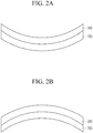
- FIG. 2A and FIG. 2B illustrate a flexible display device according to an exemplary embodiment.
- FIG. 2A illustrates a shape in which the flexible display device is bent in a direction in which the display panel 300 is compressed
- FIG. 2B illustrates a shape in which the flexible display device is bent in a direction in which the display panel 300 is stretched.
- the display panel 300 of the display device according to an exemplary embodiment may be bendable in opposite directions, including the stretched direction and the compressed direction.
- stress may accumulate in the metal layer 710 of the base film 700 due to repeated bending in the opposite directions.
- the first layer 720 and the second layer 730 including the polymer material at opposite sides of the metal layer 710 of the base film 700, it may be possible to increase the yield strain at which the base film 700 is broken and to prevent the base film 700 from being damaged.
- FIG. 3 and FIG. 4 separately illustrate a base film 700 from a display device according to an exemplary embodiment.
- the first layer 720 and the second layer 730 of the base film 700 may include the same material.
- the base film 700 may include Invar, and the first layer 720 and the second layer 730 may include polyimide.
- the base film 700 may include Invar, and the first layer 720 and the second layer 730 may include polyethylethylketone.
- the first layer 720 and the second layer 730 of the base film 700 may include different materials.
- the metal layer 710 may include Invar
- the first layer 720 may include polyimide
- the second layer 730 may include polyethylethylketone.
- a polymer material having a high modulus when included in a layer positioned on an outside with respect to a bending direction, for example, a layer to which a tension force is applied, and when a polymer material having a low modulus is included in a layer positioned at an inside of the bending direction, that is, a layer to which compressive stress is applied, it may be possible to effectively prevent the base film 700 from being broken.
- FIG. 5 illustrates a base film 700 of a display device according to another exemplary embodiment.
- the metal layer may include a first metal layer 710a and a second metal layer 710b.
- a polymer layer may include the first layer 720 positioned on one surface of the first metal layer 710a, the second layer 730 positioned on one surface of the second metal layer 710b, and a third layer 740 positioned between the first metal layer 710a and the second metal layer 710b.
- the metal layers 710a and 701b and the first layer to the third layer 720, 730, and 740 may have the same composition as the first and second layers 720 and 730 and the metal layer 710 as described above. The detailed description of the same constituent elements will not be repeated.
- the base film according to the embodiment of FIG. 5 may have a five-layer structure of a polymer-metal-polymer-metal-polymer, in contrast to the base film according to the previous embodiment, which was a three-layer structure of a polymer-metal-polymer.
- the first metal layer 710a and the second metal layer 710b may include the same material, or may include different materials.
- the first layer 720, the second layer 730, and the third layer 740 may include the same material, or may include different materials. Similar to FIG. 4 , in the base film according to the embodiment of FIG. 5 , the materials with different moduli may be sequentially included in respective layers according to anticipated bending directions.
- the polymer material when the base film 700 is more likely to be bent in the direction in which the first layer 720 is compressed, the polymer material may be included such that the moduli increase in an order of the first layer 720, the third layer 740, and the second layer 730.
- a material having a greater modulus than in the first metal layer 710a may be included in the second metal layer 710b.
- FIG. 6 schematically illustrates an entire stacked structure of a display device according to an exemplary embodiment.
- a display device may include a jig 1300 for fixing the display device, a cover panel 1200 positioned on the jig and having a cushion structure, the base film 700 positioned on the cover panel 1200, the display panel 300 positioned on the base film 700, the polarizer 400 positioned on the display panel, the touch panel 500 positioned on the polarizer, the window 600 positioned on the touch panel 500, and the passivation film 1100 positioned on the window.
- the respective constituent elements may be bonded to each other by an adhesive layer 60.
- a stacked order of the constituent elements may vary from what is described above, and some of the constituent elements may be omitted.
- the display panel 300 may be positioned in a central region of the display device due to the presence of the base film 700.
- the base film 700 includes the metal layer 710 with a high modulus, such that the central layer of the display device may be positioned in the display panel 300.
- the first layer 720 and the second layer 730 including the polymer material may be positioned at opposite sides of the metal layer 710, thereby helping to prevent the metal layer 710 from being broken due to repeated bending.
- Table 1 shows measured yield strains when the base film is formed as a single metal layer including Invar. (Table 1) Measured value of single Invar 40 ⁇ m 30 ⁇ m Strain (@R3) 1.1% 1.7%
- FIG. 7 illustrates an image of the cracked Invar film.
- Table 2 shows measured moduli and yield strains of the base film made of an Invar monolayer (Comparative Example 1), and moduli and yield strains of the base film made of a polyimide/Invar/polyimide triple layer (Exemplary Embodiment 1).
- the display panel 300 described above may be a liquid crystal display panel or a light emitting display panel, as examples.
- the display panel 300 may include the first substrate 110.
- the first substrate 110 may be flexible.
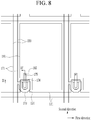
- FIG. 8 illustrates a layout view of a display panel according to an exemplary embodiment
- FIG. 9 illustrates a cross-sectional view taken along line IX-IX' of the display device of FIG. 8 .
- the display panel 300 includes a first display panel 100, a second display panel 200 overlapping the first display panel 100, and the liquid crystal layer 3 positioned between the first display panel 100 and the second display panel 200.
- the first display panel 100 may include a gate conductor including a gate line 121 and a gate electrode 124 positioned on one surface of the first substrate 110.
- the first substrate 110 may be made of transparent glass or plastic.
- the gate line 121 may extend in a first direction.
- the gate conductor may include a suitable metal or conductor, and may have a multi-layered structure.
- a gate insulating layer 140 may be positioned between the gate conductor and the liquid crystal layer 3.
- the gate insulating layer 140 may include an inorganic insulating material.
- a semiconductor layer 154 may be positioned on one surface of the gate insulating layer 140.
- a data line 171 may be positioned between the semiconductor layer 154 and the liquid crystal layer 3.
- the data line 171 may extend in a second direction to cross the gate line 121.
- a source electrode 173 may extend from the data line 171 and may overlap the gate electrode 124.
- a drain electrode 175 may be separated from the data line 171. As shown in FIG. 8 , the drain electrode may be rod-shaped and extend toward a center of the source electrode 173.
- the semiconductor layer 154 may not overlap the data line 171 and the drain electrode 175 in a region between the source electrode 173 and the drain electrode 175.
- the semiconductor layer 154 may have substantially the same planar shape as the data line 171 and the drain electrode 175 except for the non-overlapping portion.
- One gate electrode 124, one source electrode 173, and one drain electrode 175 may form one thin film transistor together with the semiconductor layer 154.
- a channel of the thin film transistor may correspond to a region of the semiconductor layer 154 between the source electrode 173 and the drain electrode 175.
- a passivation layer 180 may be positioned between the source electrode 173 and drain electrode 175, and the liquid crystal layer 3.
- the passivation layer 180 may include an inorganic insulating material, an organic insulating material, a low dielectric insulating material, etc., such as a silicon nitride or a silicon oxide.
- the passivation layer 180 may be provided with a contact hole 185 overlapping some of the drain electrode 175.
- a first electrode 191 may be positioned between the passivation layer 180 and the liquid crystal layer 3.
- the first electrode 191 may be physically and electrically connected to the drain electrode 175 through the contact hole 185.
- the first electrode 191 may receive a data voltage from the drain electrode 175.
- the first electrode 191 may be a pixel electrode.
- a first alignment layer 11 may be positioned between the first electrode 191 and the liquid crystal layer 3.
- the second display panel 200 may include the second substrate 210, a light blocking member 220, a second electrode 270, and a second alignment layer 21.
- the second electrode 270 may be positioned on one surface of the second substrate 210.
- the second electrode 270 may be a common electrode.
- the light blocking member 220 may be positioned between the second substrate 210 and the second electrode 270.
- the light blocking member 220 may overlap the data line 171 to extend in the second direction.
- the light blocking member may further include a horizontal portion overlapping the gate line 121 and extending in the first direction. In some implementations, the light blocking member 220 may be omitted.
- the second alignment layer 21 may be positioned between the second electrode 270 and the liquid crystal layer 3.
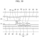
- FIG. 10 illustrates a cross-sectional view of a display panel according to an exemplary embodiment.
- a buffer layer 111 made of a silicon oxide or a silicon nitride may be positioned on the first substrate 110.
- a semiconductor layer 154 may be positioned on the buffer layer 111.
- the semiconductor layer 154 may include a source region 153 and a drain region 155 doped with a p-type impurity, and a channel region 151 positioned between the source region 153 and the drain region 155.
- a gate insulating layer 140 may be positioned on the semiconductor layer 154 and the buffer layer 111.
- the gate insulating layer 140 may include a silicon oxide or a silicon nitride.
- the gate electrode 124 may overlap the channel region 151 of the semiconductor layer 154 and may be positioned on the gate insulating layer 140.
- An interlayer insulating layer 160 may be positioned on the gate electrode 124 and the gate insulating layer 140.
- the interlayer insulating layer 160 may be provided with a first contact hole 165 and a second contact hole 163.
- a data conductor including a data line 171, a source electrode 173, and a drain electrode 175 may be positioned on the interlayer insulating layer 160.
- the drain electrode 175 may be connected to the drain region 155 through the first contact hole 165.
- the source electrode 173 may be connected to the source region 153 through the second contact hole 163.
- a passivation layer 180 may be positioned on the data conductors 171, 173, and 175 and the interlayer insulating layer 160.
- the passivation layer 180 may be provided with a contact hole 185.
- the first electrode 191 may be positioned on the passivation layer 180.
- the first electrode 191 may be a pixel electrode.
- the first electrode 191 may be connected to the drain electrode 175 through the contact hole 185.
- a partition wall 361 may be positioned on the passivation layer 180.
- a light-emitting diode layer 370 may be positioned to overlap the first electrode 191, and the second electrode 270 is positioned to overlap the light-emitting diode layer 370.
- the second electrode 270 may be a common electrode.
- the first electrode 191 may be an anode, which is a hole injection electrode, and the second electrode 270 may be a cathode, which is an electron injection electrode.
- the first electrode 191 may be a cathode and the second electrode 270 may be an anode.
- the light-emitting diode layer 370 may include an emission layer, an electron transporting layer, a hole transporting layer, etc.
- An encapsulation layer 390 may be positioned to overlap the second electrode 270.
- the encapsulation layer 390 may include an organic material or an inorganic material, or may include the organic material and the inorganic material that are alternately stacked.
- the encapsulation layer 390 may protect the display device from external moisture, heat, and other pollutants.
- the display device may include the base film 700 positioned at a lower portion of the display panel 300.
- the base film 700 may have a structure in which the metal layer 710 is positioned between the first layer 720 and the second layer 730 including the polymer material. Accordingly, the display panel 300 may be located in a central layer of the display device due to the presence of the metal layer 710, and damage to the display panel 300 is minimized even when the display device is bent.
- the first layer 720 and the second layer 730 including the polymer material may be positioned at the opposite sides of the metal layer 710, of the display device, thereby helping to prevent the metal layer 710 from being damaged by the bending of the display device.
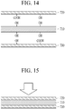
- FIG. 11 to FIG. 15 illustrate manufacturing processes of the base film according to the exemplary embodiment.
- the metal layer 710 may be formed.
- the metal layer 710 may include at least one of Invar, stainless steel, titanium, and copper.
- the thickness of the metal layer 710 may be from 20 ⁇ m to 30 ⁇ m.
- the first layer 720 and the second layer 730 may be respectively positioned at upper and lower portions of the metal layer 710.
- Each of the first layer 720 and the second layer 730 may include a polymer material.
- the modulus of the polymer material included in each of the first layer 720 and the second layer 730 may be from 1 GPa to 10 GPa.
- the thickness of each of the first layer 720 and the second layer 730 may be from 7 ⁇ m to 15 ⁇ m.
- the first layer 720 and the second layer 730 may include at least one of polyimide, polyphenylene sulfide, polyethylene naphthalate, and polyaryletherketone.
- the first layer 720 and the second layer 730 may include the same material, or may include different materials.
- plasma may be supplied between the metal layer 710 and the first layer 720 and between the metal layer 720 and the second layer 730 to activate the surfaces of the metal layer 710, the first layer 720, and the second layer 730.
- -COOH groups or -OH groups positioned on the surface of the metal layer 710, the first layer 720, and the second layer 730 may be activated.
- FIG. 14 schematically illustrates the activated surfaces of the metal layer 710, the first layer 720, and the second layer 730.
- FIG. 14 exemplarily illustrates some reactive groups.
- pressure may be applied to the surfaces of the metal layer 710, the first layer 720, and the second layer 730 that are activated in FIG. 14 .
- the pressure may cause the activated reactive groups, for example, -COOH groups and -OH groups, to react and bind with each other on the surfaces of the metal layer 710, the first layer 720, and the second layer 730.
- Reaction equations may be as follows. COOH + OH ⁇ COO + H 2 O OH + OH ⁇ O + H 2 O
- the metal layer 710 and the first layer 720, and the metal layer 710 and the second layer 730 may be bonded to each other without an adhesive layer or an adhesive by the reaction equations. Therefore, the base film 700 may be manufactured by bonding the first layer 720, the metal layer 710, and the second layer 730 to each other without an adhesive or an adhesive layer.
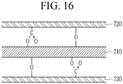
- FIG. 16 illustrates a combination principle between the metal layer 710 and the first layer 720 and between the metal layer 710 and the second layer 730 according to the manufacturing method.
- -OH or -COOH groups activated by the plasma may react with -OH or -COOH groups in an adjacent layer by the pressure to form - COO- bonds or -O- bonds. Consequently, adjacent layers may be bonded to each other without a separate adhesive layer.
- the metal layer 710 may be bonded to the first layer 720 and the second layer 730 without using an adhesive layer or an adhesive, which is economical.
- an adhesive or adhesive layer were to be used, the characteristics of the base film 700 could be changed or the central layer of the display device to which the base film 700 is applied could be changed due to the presence of the adhesive or adhesive layer.
- this issue may be avoided because the base film 700 according to the present exemplary embodiment does not have the adhesive or adhesive layer.
- the liquid crystal display is a non-emissive display device that uses a separate light source such as a backlight.
- an organic light emitting diode (OLED) display that is a self-luminous display device has received attention.
- the organic light emitting diode display includes two electrodes facing each other, and an organic layer interposed between the electrodes. In the organic light emitting diode display, if holes injected from an anode and electrons injected from a cathode meet each other at a light emitting layer to generate an exciton and the exciton is subjected to photo-luminescence quenching, light is generated.
- the organic light emitting diode display may be applied to various fields including a display device and a lighting device.
- a flexible display device can be configured by using a bendable substrate.
- constituent elements such as pixels and/or wires formed in the flexible display device may have bent or folded portions which may be deformed or of which the characteristics may be deteriorated due to stress.
- Embodiments provide a display device that reduces damage when the display device is bent and a method of manufacturing a base film without using an adhesive layer.
Landscapes
- Physics & Mathematics (AREA)
- Nonlinear Science (AREA)
- Chemical & Material Sciences (AREA)
- Optics & Photonics (AREA)
- General Physics & Mathematics (AREA)
- Mathematical Physics (AREA)
- Crystallography & Structural Chemistry (AREA)
- Inorganic Chemistry (AREA)
- Devices For Indicating Variable Information By Combining Individual Elements (AREA)
- Fluid Mechanics (AREA)
- Engineering & Computer Science (AREA)
- Theoretical Computer Science (AREA)
- Spectroscopy & Molecular Physics (AREA)
- Electroluminescent Light Sources (AREA)
Abstract
Description
- Embodiments relate to a display device and a manufacturing method of a base film included in the display device.
- A liquid crystal display (LCD), an organic light emitting diode (OLED) display, etc., may be used as a display device. To apply these display devices to various applications, a flexible display device that can be easily bent has been developed.
- Embodiments are directed to a display device including a display panel including a substrate and a base film positioned on one surface of the display panel. The base film includes a first layer and a second layer overlapping each other, and a metal layer positioned between the first layer and the second layer. A modulus (Young's modulus) of each of the first layer and the second layer is from 1 GPa to 10 GPa.
- Each of the first layer and the second layer may include at least one of polyimide, polyphenylene sulfide, polyethylene naphthalate, and polyaryletherketone.
- The metal layer may include at least one of Invar, stainless steel, titanium, and copper.
- A thickness of the metal layer may be greater than a sum of thicknesses of the first layer and the second layer.
- A thickness of the metal layer may be from 20 µm to 30 µm.
- A thickness of each of the first layer and the second layer may be from 7 µm to 15 µm.
- The first layer and the second layer may include a same material.
- The first layer and the second layer may include different materials.
- The metal layer may include a first metal layer and a second metal layer, and a third layer positioned between the first metal layer and the second metal layer. The first metal layer may be positioned between the first layer and the third layer. The second metal layer may be positioned between the second layer and the third layer.
- The first metal layer and the second metal layer may include a same material.
- The first metal layer and the second metal layer may include different materials.
- The display device may be flexible. The display device may be bendable in respective directions in which the display panel is compressible and stretchable.
- The display panel may be a light emitting display panel or a liquid crystal display panel.
- The metal layer may include Invar, and the first layer and the second layer may include polyimide.
- The metal layer includes Invar, the first layer may include polyimide, and the second layer may include polyaryletherketone.
- There may not be an adhesive layer positioned between the metal layer and the first layer or between the metal layer and the second layer. A reactive group on a surface of the metal layer may be directly bonded to reactive groups on surfaces of the first layer and the second layer.
- Embodiments are also directed to manufacturing method of a base film, the manufacturing method including preparing a metal layer, positioning a first layer and a second layer at opposite sides of the metal layer, activating reactive groups on surfaces of the metal layer, the first layer, and the second layer by supplying plasma between the metal layer and the first layer and between the metal layer and the second layer, and bonding the first layer, the metal layer, and the second layer by applying pressure to the first layer, the metal layer, and the second layer, wherein a modulus of each of the first layer and the second layer is from 1 GPa to 10 GPa.
- Each of the first layer and the second layer may include at least one of polyimide, polyphenylene sulfide, polyethylene naphthalate, and polyaryletherketone. The metal layer may include at least one of Invar, stainless steel, titanium, and copper.
- In activating the reactive groups on the surfaces of the metal layer, the first layer, and the second layer by supplying the plasma between the metal layer and the first layer and between the metal layer and the second layer, -OH or -COOH groups positioned on the surfaces of the first layer, the metal layer, and the second layer may be activated.
- In bonding the first layer, the metal layer, and the second layer by applying the pressure to the first layer, the metal layer, and the second layer, -OH groups of layers contacting each other may react to form -O- bonds, or -OH and -COOH groups of layers contacting each other may react to form -COO- bonds.
- According to an aspect of the invention, there is provided a display device as set out in claim 1. Preferred features of this aspect are set out in claims 2 to 15.
- Features will become apparent to those of skill in the art by describing in detail exemplary embodiments with reference to the attached drawings in which:
-
FIG. 1 schematically illustrates a cross-sectional view of a display device according to an exemplary embodiment. -
FIG. 2 illustrates a flexible display device according to an exemplary embodiment. -
FIG. 3 and FIG. 4 separately illustrate a base film from a display device according to an exemplary embodiment. -
FIG. 5 illustrates a base film of a display device according to an exemplary embodiment. -
FIG. 6 schematically illustrates an entire stacked structure of a display device according to an exemplary embodiment. -
FIG. 7 illustrates an image of an Invar film in which a crack has occurred. -
FIG. 8 illustrates a layout view of a display panel according to an exemplary embodiment, andFIG. 9 illustrates a cross-sectional view taken along line IX-IX' of the display device ofFIG. 8 . -
FIG. 10 illustrates a cross-sectional view of a display panel according to an exemplary embodiment. -
FIG. 11 to FIG. 15 illustrate manufacturing processes of a base film according to an exemplary embodiment. -
FIG. 16 illustrates a combination principle between a metal layer and a first layer and between a metal layer and a second layer according to a manufacturing method. - Example embodiments will now be described more fully hereinafter with reference to the accompanying drawings; however, they may be embodied in different forms and should not be construed as limited to the embodiments set forth herein. Rather, these embodiments are provided so that this disclosure will be thorough and complete, and will fully convey exemplary implementations to those skilled in the art.
- In the drawing figures, the dimensions of layers and regions may be exaggerated for clarity of illustration. Like reference numerals refer to like elements throughout.
-
FIG. 1 schematically illustrates a cross-sectional view of a display device according to an exemplary embodiment. Referring toFIG. 1 , a display device according to an exemplary embodiment includes abase film 700 having a multi-layered structure, and adisplay panel 300 positioned on the base film. - Referring to
FIG. 1 , thedisplay panel 300 in some implementations may include afirst substrate 110, asecond substrate 210 overlapping the first substrate, and aliquid crystal layer 3 positioned between the first and second substrates. In some implementations, thedisplay panel 300 may be an emissive display device including light-emitting elements and not including theliquid crystal layer 3. Thedisplay panel 300 may include thefirst substrate 110 in which a transistor or the like are positioned. As will be described in detail below, thedisplay panel 300 in some implementations may have a cross-sectional structure as shown inFIG. 9 orFIG. 10 . - Referring to
FIG. 1 , thebase film 700 may include ametal layer 710, and afirst layer 720 andsecond layer 730 positioned at opposite sides of themetal layer 710. Themetal layer 710 may include, for example, at least one of Invar, stainless steel, titanium, and copper. - The
base film 700 may be positioned to be adjacent to thedisplay panel 300. Thebase film 700 may include themetal layer 710 to balance the display device. The display device may include, apolarizer 400, atouch panel 500, a window 600, and apassivation film 1100 that are positioned on thedisplay panel 300, as shown inFIG. 6 and described in more detail below. In contrast, when only ajig 1300 or acover panel 1200 is positioned below thedisplay panel 300, a lower portion of the display device may not have a structure with a high modulus or a thick thickness. Therefore, upper and lower portions of the display device may be unbalanced based on thedisplay panel 300. In this case, when the display device is bent, a large amount of stress may be applied to thedisplay panel 300, and thus a transistor or the like positioned on thedisplay panel 300 may be susceptible to damage. - However, the display device according to the exemplary embodiment includes the
base film 700, which includes themetal layer 710, positioned below thedisplay panel 300. Themetal layer 710 may have a high modulus of 50 GPa or more. Accordingly, the upper and lower portions of the display device may be balanced with respect to thedisplay panel 300. By adding themetal layer 710, thedisplay panel 300 may become a central layer of the display device. Accordingly, by positioning thebase film 700 including themetal layer 710 below thedisplay panel 300, the display panel may become the layer to which stress is minimally applied when the display device is bent, thereby preventing thedisplay panel 300 from being damaged due to bending. - The
metal layer 710 included in thebase film 700 may include a material having a high modulus in order to balance with the upper structure of thedisplay panel 300. For example, themetal layer 710 may include a material having a modulus of 50 GPa or more. Themetal layer 710 may include at least one of Invar, stainless steel, titanium, and copper, as examples. Among them, Invar, which is an alloy of iron and nickel, specifically, an alloy having 63.5 % of iron and 36.5 % of nickel has a small thermal expansion coefficient. Invar is desirable as a material of themetal layer 710 because it is easy to process in a form of a metal layer, has a high modulus (58.8 GPa), and has a moisture absorption rate of 0 %. - The
metal layer 710 may serve not only to balance the display device, but also to support thedisplay panel 300 and to prevent damage from external impact. However, if thebase film 700 were to be formed as a single layer including only themetal layer 710, stress could be concentrated on themetal layer 710 when the display device is repeatedly bent and themetal layer 710 could be broken. - However, the
base film 700 of the display device according to the exemplary embodiment includes themetal layer 710, and thefirst layer 720 and thesecond layer 730, including a polymer material, contacting opposite sides of themetal layer 710, and thefirst layer 720 and thesecond layer 730. Thefirst layer 720 and thesecond layer 730 may include a general polymer material. As examples, thefirst layer 720 and thesecond layer 730 may include at least one of polyimide, polyphenylene sulfide, polyethylene naphthalate, and polyaryletherketone. - The
first layer 720 and thesecond layer 730 including such a polymer material, may prevent thebase film 700 including themetal layer 710 from being broken when the display device is bent, for example, in a region that is repeatedly bent. Thefirst layer 720 and thesecond layer 730 including the polymer material may increase the yield strain at which the base film begins to break, thereby preventing damage to the base film even when the display device is repeatedly bent. - A modulus of each polymer material included in the
first layer 720 and thesecond layer 730 may be from 1 GPa to 10 GPa. When the modulus of the polymer material respectively included in thefirst layer 720 and thesecond layer 730 is more than 1 GPa, the effect of preventing the damage of themetal layer 710 according to the addition of thefirst layer 720 and thesecond layer 730 may be sufficient. When the modulus of the polymer material included in thefirst layer 720 and thesecond layer 730 is less than 10 GPa, the elasticity of thefirst layer 720 and thesecond layer 730 may be maintained. That is, a situation may be avoided wherein thefirst layer 720 and thesecond layer 730 fail to absorb the impact of thebase film 700 and are broken together with themetal layer 710. Therefore, the modulus of the polymer material respectively included in thefirst layer 720 and thesecond layer 730 may be from 1 GPa to 10 GPa. - In an exemplary embodiment, a thickness of the
metal layer 710 may be from 20 µm to 30 µm. Thicknesses of thefirst layer 720 and thesecond layer 730 may be from 7 µm to 15 µm, respectively. In an exemplary embodiment, the thickness of themetal layer 710 may be greater than a sum of the thicknesses of thefirst layer 720 and thesecond layer 730. When the thickness of themetal layer 710 is greater than the sum of the thicknesses of thefirst layer 720 and thesecond layer 730, structural reinforcement of thedisplay panel 300 by thebase film 700 may be sufficiently achieved. In addition, in the display device according to an exemplary embodiment a position of the central layer of the display device is at thedisplay panel 300 because of thebase film 700 including themetal layer 710. When the thickness of themetal layer 710 is greater than the sum of the thicknesses of thefirst layer 720 and thesecond layer 730, a position of the central surface may be maintained. - In the
base film 700 according to an exemplary embodiment, themetal layer 710 and thefirst layer 720, and themetal layer 710 and thesecond layer 730, are directly bonded without adhesive or an adhesive layer therebetween. For example, an adhesive layer or adhesive may be omitted between themetal layer 710 and thefirst layer 720 or between themetal layer 710 and thesecond layer 730. - In the
base film 700 according to an exemplary embodiment, themetal layer 710, thefirst layer 720, and thesecond layer 730 may be combined by surface activated bonding, which is a method of bonding substrates by supplying a plasma between both substrates to activate reactors such as -OH or -COOH groups on surfaces of both substrates, and then pressing both substrates against each other with a strong pressure to allow the activated reactors to be bonded to each other. For example, in an exemplary embodiment, the -OH groups positioned on the surface of themetal layer 710 may be directly bonded to the -OH groups positioned on the surfaces of thefirst layer 720 and thesecond layer 730. - As described above, the
base film 700 may not include an adhesive layer or adhesive. Accordingly, it may be possible to prevent physical properties of thebase film 700 from being changed due to the presence of an adhesive layer or an adhesive. It may be possible to prevent the central layer of the display device from being moved due to the presence of an adhesive layer or an adhesive. For example, if an adhesive layer were to be included therein, characteristics of thebase film 700 could be changed at an interface between the adhesive layer and themetal layer 710 and at an interface between the adhesive layer and thefirst layer 720 or thesecond layer 730. When the display device according to an exemplary embodiment does not include an adhesive layer, it may be possible to prevent undesirable issues resulting from the presence of an adhesive layer. - The display device according to an exemplary embodiment may be a flexible display device. For example, the display device according to an embodiment may be a display device that is bendable in upward and downward directions of the display panel.
-
FIG. 2A and FIG. 2B illustrate a flexible display device according to an exemplary embodiment.FIG. 2A illustrates a shape in which the flexible display device is bent in a direction in which thedisplay panel 300 is compressed, andFIG. 2B illustrates a shape in which the flexible display device is bent in a direction in which thedisplay panel 300 is stretched. For example, as shown inFIG. 2A and FIG. 2B , thedisplay panel 300 of the display device according to an exemplary embodiment may be bendable in opposite directions, including the stretched direction and the compressed direction. - In this case, stress may accumulate in the
metal layer 710 of thebase film 700 due to repeated bending in the opposite directions. However, in the display device according to an exemplary embodiment, by positioning thefirst layer 720 and thesecond layer 730 including the polymer material at opposite sides of themetal layer 710 of thebase film 700, it may be possible to increase the yield strain at which thebase film 700 is broken and to prevent thebase film 700 from being damaged. -
FIG. 3 and FIG. 4 separately illustrate abase film 700 from a display device according to an exemplary embodiment. Referring toFIG. 3 , thefirst layer 720 and thesecond layer 730 of thebase film 700 may include the same material. For example, thebase film 700 may include Invar, and thefirst layer 720 and thesecond layer 730 may include polyimide. As another example, thebase film 700 may include Invar, and thefirst layer 720 and thesecond layer 730 may include polyethylethylketone. - Referring to
FIG. 4 , thefirst layer 720 and thesecond layer 730 of thebase film 700 may include different materials. For example, themetal layer 710 may include Invar, thefirst layer 720 may include polyimide, and thesecond layer 730 may include polyethylethylketone. When a direction in which the flexible display device is mainly bent is specified, stress and strain may be appropriately adjusted in the stretched layer and the compressed layer by including polymer materials having different moduli in thefirst layer 720 and thesecond layer 730. - For example, when a polymer material having a high modulus is included in a layer positioned on an outside with respect to a bending direction, for example, a layer to which a tension force is applied, and when a polymer material having a low modulus is included in a layer positioned at an inside of the bending direction, that is, a layer to which compressive stress is applied, it may be possible to effectively prevent the
base film 700 from being broken. -
FIG. 5 illustrates abase film 700 of a display device according to another exemplary embodiment. Referring toFIG. 5 , in thebase film 700 according to an exemplary embodiment, the metal layer may include afirst metal layer 710a and asecond metal layer 710b. A polymer layer may include thefirst layer 720 positioned on one surface of thefirst metal layer 710a, thesecond layer 730 positioned on one surface of thesecond metal layer 710b, and athird layer 740 positioned between thefirst metal layer 710a and thesecond metal layer 710b. Themetal layers 710a and 701b and the first layer to thethird layer second layers metal layer 710 as described above. The detailed description of the same constituent elements will not be repeated. - The base film according to the embodiment of
FIG. 5 may have a five-layer structure of a polymer-metal-polymer-metal-polymer, in contrast to the base film according to the previous embodiment, which was a three-layer structure of a polymer-metal-polymer. Thefirst metal layer 710a and thesecond metal layer 710b may include the same material, or may include different materials. Similarly, thefirst layer 720, thesecond layer 730, and thethird layer 740 may include the same material, or may include different materials. Similar toFIG. 4 , in the base film according to the embodiment ofFIG. 5 , the materials with different moduli may be sequentially included in respective layers according to anticipated bending directions. For example, when thebase film 700 is more likely to be bent in the direction in which thefirst layer 720 is compressed, the polymer material may be included such that the moduli increase in an order of thefirst layer 720, thethird layer 740, and thesecond layer 730. Similarly, in the metal layer, a material having a greater modulus than in thefirst metal layer 710a may be included in thesecond metal layer 710b. When thebase film 700 is more likely bent in the direction in which thesecond layer 730 is compressed, the layers of the base film may be opposite to the above description. -
FIG. 6 schematically illustrates an entire stacked structure of a display device according to an exemplary embodiment. Referring toFIG. 6 , a display device according to an exemplary embodiment may include ajig 1300 for fixing the display device, acover panel 1200 positioned on the jig and having a cushion structure, thebase film 700 positioned on thecover panel 1200, thedisplay panel 300 positioned on thebase film 700, thepolarizer 400 positioned on the display panel, thetouch panel 500 positioned on the polarizer, the window 600 positioned on thetouch panel 500, and thepassivation film 1100 positioned on the window. The respective constituent elements may be bonded to each other by anadhesive layer 60. - A stacked order of the constituent elements may vary from what is described above, and some of the constituent elements may be omitted. Referring to
FIG. 6 , thedisplay panel 300 may be positioned in a central region of the display device due to the presence of thebase film 700. Thebase film 700 includes themetal layer 710 with a high modulus, such that the central layer of the display device may be positioned in thedisplay panel 300. Moreover, thefirst layer 720 and thesecond layer 730 including the polymer material may be positioned at opposite sides of themetal layer 710, thereby helping to prevent themetal layer 710 from being broken due to repeated bending. - Table 1 shows measured yield strains when the base film is formed as a single metal layer including Invar.
(Table 1) Measured value of single Invar 40 µm 30 µm Strain (@R3) 1.1% 1.7% - Referring to Table 1, when the base film was bent at a curvature (@ R3) of 3 mm, it can be seen that the Invar film having a thickness of 40 µm cracked at a strain of 1.1 % and the Invar film having a thickness of 30 µm cracked at a strain of 1.7 %.
FIG. 7 illustrates an image of the cracked Invar film. - Table 2 shows measured moduli and yield strains of the base film made of an Invar monolayer (Comparative Example 1), and moduli and yield strains of the base film made of a polyimide/Invar/polyimide triple layer (Exemplary Embodiment 1).
(Table 2) Base film 30 µm Modulus [GPa] Yield strain [%] Comparative Example 1 (Invar) 58.86 1.86 Exemplary Embodiment 1 (PI/Invar/PI) 66.17 2.21 - Referring to Table 2, it was confirmed that the modulus and the yield strain value increased at the same thickness in Example 1 compared with Comparative Example 1. For example, by positioning the polyimide layer on the opposite sides of the Invar film, it was confirmed that mechanical properties thereof were improved as compared with those of the Invar monolayer.
- The
display panel 300 described above may be a liquid crystal display panel or a light emitting display panel, as examples. Thedisplay panel 300 may include thefirst substrate 110. When the display device is a flexible display device, thefirst substrate 110 may be flexible. - Hereinafter, a specific structure in which the
display panel 300 may be included will be described with reference to the accompanying drawings. -
FIG. 8 illustrates a layout view of a display panel according to an exemplary embodiment, andFIG. 9 illustrates a cross-sectional view taken along line IX-IX' of the display device ofFIG. 8 . - Referring to
FIG. 8 andFIG. 9 , thedisplay panel 300 includes afirst display panel 100, asecond display panel 200 overlapping thefirst display panel 100, and theliquid crystal layer 3 positioned between thefirst display panel 100 and thesecond display panel 200. - The
first display panel 100 may include a gate conductor including agate line 121 and agate electrode 124 positioned on one surface of thefirst substrate 110. Thefirst substrate 110 may be made of transparent glass or plastic. - The
gate line 121 may extend in a first direction. The gate conductor may include a suitable metal or conductor, and may have a multi-layered structure. Agate insulating layer 140 may be positioned between the gate conductor and theliquid crystal layer 3. Thegate insulating layer 140 may include an inorganic insulating material. - A
semiconductor layer 154 may be positioned on one surface of thegate insulating layer 140. - A
data line 171 may be positioned between thesemiconductor layer 154 and theliquid crystal layer 3. Thedata line 171 may extend in a second direction to cross thegate line 121. Asource electrode 173 may extend from thedata line 171 and may overlap thegate electrode 124. Adrain electrode 175 may be separated from thedata line 171. As shown inFIG. 8 , the drain electrode may be rod-shaped and extend toward a center of thesource electrode 173. - Some of the
semiconductor layer 154 may not overlap thedata line 171 and thedrain electrode 175 in a region between thesource electrode 173 and thedrain electrode 175. Thesemiconductor layer 154 may have substantially the same planar shape as thedata line 171 and thedrain electrode 175 except for the non-overlapping portion. - One
gate electrode 124, onesource electrode 173, and onedrain electrode 175 may form one thin film transistor together with thesemiconductor layer 154. A channel of the thin film transistor may correspond to a region of thesemiconductor layer 154 between thesource electrode 173 and thedrain electrode 175. - A
passivation layer 180 may be positioned between thesource electrode 173 anddrain electrode 175, and theliquid crystal layer 3. Thepassivation layer 180 may include an inorganic insulating material, an organic insulating material, a low dielectric insulating material, etc., such as a silicon nitride or a silicon oxide. - The
passivation layer 180 may be provided with acontact hole 185 overlapping some of thedrain electrode 175. - A
first electrode 191 may be positioned between thepassivation layer 180 and theliquid crystal layer 3. Thefirst electrode 191 may be physically and electrically connected to thedrain electrode 175 through thecontact hole 185. Thefirst electrode 191 may receive a data voltage from thedrain electrode 175. Thefirst electrode 191 may be a pixel electrode. - A
first alignment layer 11 may be positioned between thefirst electrode 191 and theliquid crystal layer 3. - The
second display panel 200 may include thesecond substrate 210, alight blocking member 220, asecond electrode 270, and asecond alignment layer 21. - The
second electrode 270 may be positioned on one surface of thesecond substrate 210. Thesecond electrode 270 may be a common electrode. - The
light blocking member 220 may be positioned between thesecond substrate 210 and thesecond electrode 270. Thelight blocking member 220 may overlap thedata line 171 to extend in the second direction. The light blocking member may further include a horizontal portion overlapping thegate line 121 and extending in the first direction. In some implementations, thelight blocking member 220 may be omitted. - The
second alignment layer 21 may be positioned between thesecond electrode 270 and theliquid crystal layer 3. - Hereinafter, a display device according to another exemplary embodiment will be described in detail with reference to
FIG. 10 . -
FIG. 10 illustrates a cross-sectional view of a display panel according to an exemplary embodiment. Referring toFIG. 10 , abuffer layer 111 made of a silicon oxide or a silicon nitride may be positioned on thefirst substrate 110. - A
semiconductor layer 154 may be positioned on thebuffer layer 111. Thesemiconductor layer 154 may include asource region 153 and adrain region 155 doped with a p-type impurity, and achannel region 151 positioned between thesource region 153 and thedrain region 155. - A
gate insulating layer 140 may be positioned on thesemiconductor layer 154 and thebuffer layer 111. Thegate insulating layer 140 may include a silicon oxide or a silicon nitride. Thegate electrode 124 may overlap thechannel region 151 of thesemiconductor layer 154 and may be positioned on thegate insulating layer 140. - An interlayer insulating
layer 160 may be positioned on thegate electrode 124 and thegate insulating layer 140. The interlayer insulatinglayer 160 may be provided with afirst contact hole 165 and asecond contact hole 163. - A data conductor including a
data line 171, asource electrode 173, and adrain electrode 175 may be positioned on theinterlayer insulating layer 160. - The
drain electrode 175 may be connected to thedrain region 155 through thefirst contact hole 165. Thesource electrode 173 may be connected to thesource region 153 through thesecond contact hole 163. - A
passivation layer 180 may be positioned on thedata conductors layer 160. Thepassivation layer 180 may be provided with acontact hole 185. - The
first electrode 191 may be positioned on thepassivation layer 180. Thefirst electrode 191 may be a pixel electrode. Thefirst electrode 191 may be connected to thedrain electrode 175 through thecontact hole 185. Apartition wall 361 may be positioned on thepassivation layer 180. A light-emittingdiode layer 370 may be positioned to overlap thefirst electrode 191, and thesecond electrode 270 is positioned to overlap the light-emittingdiode layer 370. Thesecond electrode 270 may be a common electrode. - The
first electrode 191 may be an anode, which is a hole injection electrode, and thesecond electrode 270 may be a cathode, which is an electron injection electrode. In some implementations, according to a driving method of the display device, thefirst electrode 191 may be a cathode and thesecond electrode 270 may be an anode. - The light-emitting
diode layer 370 may include an emission layer, an electron transporting layer, a hole transporting layer, etc. - An
encapsulation layer 390 may be positioned to overlap thesecond electrode 270. Theencapsulation layer 390 may include an organic material or an inorganic material, or may include the organic material and the inorganic material that are alternately stacked. Theencapsulation layer 390 may protect the display device from external moisture, heat, and other pollutants. - As described above, the display device according to the exemplary embodiment may include the
base film 700 positioned at a lower portion of thedisplay panel 300. Thebase film 700 may have a structure in which themetal layer 710 is positioned between thefirst layer 720 and thesecond layer 730 including the polymer material. Accordingly, thedisplay panel 300 may be located in a central layer of the display device due to the presence of themetal layer 710, and damage to thedisplay panel 300 is minimized even when the display device is bent. Thefirst layer 720 and thesecond layer 730 including the polymer material may be positioned at the opposite sides of themetal layer 710, of the display device, thereby helping to prevent themetal layer 710 from being damaged by the bending of the display device. - Hereinafter, a manufacturing method of the base film according to the exemplary embodiment will be described with reference to the accompanying drawings.
FIG. 11 to FIG. 15 illustrate manufacturing processes of the base film according to the exemplary embodiment. - Referring to
FIG. 11 , themetal layer 710 may be formed. Themetal layer 710 may include at least one of Invar, stainless steel, titanium, and copper. The thickness of themetal layer 710 may be from 20 µm to 30 µm. - Referring to
FIG. 12 , thefirst layer 720 and thesecond layer 730 may be respectively positioned at upper and lower portions of themetal layer 710. Each of thefirst layer 720 and thesecond layer 730 may include a polymer material. The modulus of the polymer material included in each of thefirst layer 720 and thesecond layer 730 may be from 1 GPa to 10 GPa. The thickness of each of thefirst layer 720 and thesecond layer 730 may be from 7 µm to 15 µm. Thefirst layer 720 and thesecond layer 730 may include at least one of polyimide, polyphenylene sulfide, polyethylene naphthalate, and polyaryletherketone. Thefirst layer 720 and thesecond layer 730 may include the same material, or may include different materials. - Referring to
FIG. 13 , plasma may be supplied between themetal layer 710 and thefirst layer 720 and between themetal layer 720 and thesecond layer 730 to activate the surfaces of themetal layer 710, thefirst layer 720, and thesecond layer 730. By supplying the plasma, -COOH groups or -OH groups positioned on the surface of themetal layer 710, thefirst layer 720, and thesecond layer 730 may be activated. -
FIG. 14 schematically illustrates the activated surfaces of themetal layer 710, thefirst layer 720, and thesecond layer 730.FIG. 14 exemplarily illustrates some reactive groups. - Referring to
FIG. 15 , pressure may be applied to the surfaces of themetal layer 710, thefirst layer 720, and thesecond layer 730 that are activated inFIG. 14 . The pressure may cause the activated reactive groups, for example, -COOH groups and -OH groups, to react and bind with each other on the surfaces of themetal layer 710, thefirst layer 720, and thesecond layer 730. - Reaction equations may be as follows.
COOH + OH → COO + H2O
OH + OH → O + H2O
- For example, the
metal layer 710 and thefirst layer 720, and themetal layer 710 and thesecond layer 730, may be bonded to each other without an adhesive layer or an adhesive by the reaction equations. Therefore, thebase film 700 may be manufactured by bonding thefirst layer 720, themetal layer 710, and thesecond layer 730 to each other without an adhesive or an adhesive layer. -
FIG. 16 illustrates a combination principle between themetal layer 710 and thefirst layer 720 and between themetal layer 710 and thesecond layer 730 according to the manufacturing method. As shown inFIG. 16 , -OH or -COOH groups activated by the plasma may react with -OH or -COOH groups in an adjacent layer by the pressure to form - COO- bonds or -O- bonds. Consequently, adjacent layers may be bonded to each other without a separate adhesive layer. - According to the manufacturing method of the base film, the
metal layer 710 may be bonded to thefirst layer 720 and thesecond layer 730 without using an adhesive layer or an adhesive, which is economical. In addition, if an adhesive or adhesive layer were to be used, the characteristics of thebase film 700 could be changed or the central layer of the display device to which thebase film 700 is applied could be changed due to the presence of the adhesive or adhesive layer. However, this issue may be avoided because thebase film 700 according to the present exemplary embodiment does not have the adhesive or adhesive layer. - By way of summation and review, display devices have been developed for various types of information transfer in modern society. Recently, many technical challenges have been addressed in terms of weight and thickness of a display device as display devices move away from flat-panel light emission.
- As one of the flat panel displays, the liquid crystal display is currently most widely used. The liquid crystal display is a non-emissive display device that uses a separate light source such as a backlight. Recently, an organic light emitting diode (OLED) display that is a self-luminous display device has received attention. The organic light emitting diode display includes two electrodes facing each other, and an organic layer interposed between the electrodes. In the organic light emitting diode display, if holes injected from an anode and electrons injected from a cathode meet each other at a light emitting layer to generate an exciton and the exciton is subjected to photo-luminescence quenching, light is generated. The organic light emitting diode display may be applied to various fields including a display device and a lighting device.
- In this organic light emitting diode display or liquid crystal display, a flexible display device can be configured by using a bendable substrate. In this case, constituent elements such as pixels and/or wires formed in the flexible display device may have bent or folded portions which may be deformed or of which the characteristics may be deteriorated due to stress.
- Embodiments provide a display device that reduces damage when the display device is bent and a method of manufacturing a base film without using an adhesive layer.
- Example embodiments have been disclosed herein, and although specific terms are employed, they are used and are to be interpreted in a generic and descriptive sense only and not for purpose of limitation. In some instances, as would be apparent to one of ordinary skill in the art as of the filing of the present application, features, characteristics, and/or elements described in connection with a particular embodiment may be used singly or in combination with features, characteristics, and/or elements described in connection with other embodiments unless otherwise specifically indicated. Accordingly, it will be understood by those of skill in the art that various changes in form and details may be made without departing from the scope as set forth in the following claims.
Claims (15)
- A display device, comprising:a display panel including a substrate; anda base film positioned on one surface of the display panel,wherein the base film includes a first layer and a second layer overlapping each other, and a metal layer positioned between the first layer and the second layer, anda modulus of each of the first layer and the second layer is from 1 GPa to 10 GPa.
- The display device as claimed in claim 1, wherein
each of the first layer and the second layer includes at least one of polyimide, polyphenylene sulfide, polyethylene naphthalate, polyaryletherketone, and polyetheretherketone. - The display device as claimed in claim 1 or 2, wherein
the metal layer includes at least one of Invar, stainless steel, titanium, and copper. - The display device as claimed in any one of claims 1 to 3, wherein
a thickness of the metal layer is greater than a sum of thicknesses of the first layer and the second layer. - The display device as claimed in any one of claims 1 to 4, wherein
a thickness of the metal layer is from 20 µm to 30 µm. - The display device as claimed in any one of claims 1 to 5, wherein
a thickness of each of the first layer and the second layer is from 7 µm to 15 µm. - The display device as claimed in any one of claims 1 to 6, wherein
the first layer and the second layer include a same material. - The display device as claimed in any one of claims 1 to 7, wherein
the first layer and the second layer include different materials. - The display device as claimed in any one of claims 1 to 8, wherein
the metal layer includes a first metal layer and a second metal layer, and a third layer positioned between the first metal layer and the second metal layer,
the first metal layer is positioned between the first layer and the third layer, and
the second metal layer is positioned between the second layer and the third layer. - The display device as claimed in claim 9, wherein
the first metal layer and the second metal layer include a same material. - The display device as claimed in claim 9, wherein
the first metal layer and the second metal layer include different materials. - The display device as claimed in any one of claims 1 to 11, wherein
the display device is flexible, and
the display device is bendable in respective directions in which the display panel is compressible and stretchable. - The display device as claimed in any one of claims 1 to 12, wherein
the metal layer includes Invar, and
the first layer and the second layer include polyimide. - The display device as claimed in any one of claims 1 to 12, wherein
the metal layer includes Invar,
the first layer includes polyimide, and
the second layer includes polyaryletherketone. - The display device as claimed in any one of claims 1 to 14, wherein
an adhesive layer is not positioned between the metal layer and the first layer or between the metal layer and the second layer, and
a reactive group on a surface of the metal layer is directly bonded to reactive groups on surfaces of the first layer and the second layer.
Applications Claiming Priority (1)
| Application Number | Priority Date | Filing Date | Title |
|---|---|---|---|
| KR1020180012946A KR102494730B1 (en) | 2018-02-01 | 2018-02-01 | Djsplay device and manufacturing method of base film |
Publications (2)
| Publication Number | Publication Date |
|---|---|
| EP3521914A1 true EP3521914A1 (en) | 2019-08-07 |
| EP3521914B1 EP3521914B1 (en) | 2020-09-23 |
Family
ID=65278262
Family Applications (1)
| Application Number | Title | Priority Date | Filing Date |
|---|---|---|---|
| EP19155119.1A Active EP3521914B1 (en) | 2018-02-01 | 2019-02-01 | Display device and manufacturing method of base film |
Country Status (4)
| Country | Link |
|---|---|
| US (1) | US11975506B2 (en) |
| EP (1) | EP3521914B1 (en) |
| KR (1) | KR102494730B1 (en) |
| CN (1) | CN110111690B (en) |
Cited By (1)
| Publication number | Priority date | Publication date | Assignee | Title |
|---|---|---|---|---|
| EP3614198A3 (en) * | 2018-08-24 | 2020-04-22 | Samsung Display Co., Ltd. | Display device including base film and manufacturing method of base film |
Families Citing this family (2)
| Publication number | Priority date | Publication date | Assignee | Title |
|---|---|---|---|---|
| KR102774295B1 (en) * | 2019-09-18 | 2025-03-05 | 삼성디스플레이 주식회사 | Window film and display device comprising it |
| KR20250162670A (en) * | 2024-05-09 | 2025-11-19 | 삼성디스플레이 주식회사 | Display device and method of manufacturing display device |
Citations (4)
| Publication number | Priority date | Publication date | Assignee | Title |
|---|---|---|---|---|
| US20140339517A1 (en) * | 2013-05-16 | 2014-11-20 | Samsung Display Co., Ltd. | Organic light-emitting diode display, an electronic device including the same, and method of manufacturing said organic light-emitting diode display |
| KR20160128649A (en) * | 2015-04-29 | 2016-11-08 | 엘지디스플레이 주식회사 | Flexible Substrate, Flexible Display Device Using the Same and Method for Manufacturing the Same |
| JP2017001390A (en) * | 2016-05-20 | 2017-01-05 | デクセリアルズ株式会社 | Conductive sheet |
| WO2017082654A1 (en) * | 2015-11-12 | 2017-05-18 | 동우 화인켐 주식회사 | Optical stack and image display device comprising same |
Family Cites Families (21)
| Publication number | Priority date | Publication date | Assignee | Title |
|---|---|---|---|---|
| US5543222A (en) | 1994-04-29 | 1996-08-06 | E. I. Du Pont De Nemours And Company | Metallized polyimide film containing a hydrocarbyl tin compound |
| US6194076B1 (en) * | 1997-04-22 | 2001-02-27 | International Business Machines Corporation | Method of forming adherent metal components on a polyimide substrate |
| WO2009075396A1 (en) * | 2007-12-12 | 2009-06-18 | Lg Electronics Inc. | Flexible film |
| KR100942555B1 (en) | 2008-02-29 | 2010-02-12 | 삼성모바일디스플레이주식회사 | Flexible substrate, manufacturing method thereof and thin film transistor using same |
| US20110311789A1 (en) * | 2008-09-12 | 2011-12-22 | Arizona Board of Regents, a body corporate acting for and on behalf of Arizona State University | Methods for Attaching Flexible Substrates to Rigid Carriers and Resulting Devices |
| KR101938125B1 (en) | 2008-12-17 | 2019-01-15 | 가부시키가이샤 한도오따이 에네루기 켄큐쇼 | Light-emitting device and electronic device |
| JP5360963B2 (en) * | 2008-12-27 | 2013-12-04 | 国立大学法人大阪大学 | Catalyst-free metallization method on dielectric substrate surface and dielectric substrate with metal film |
| CN102576735B (en) | 2009-09-30 | 2016-01-20 | 大日本印刷株式会社 | Substrate for flexible device, thin film transistor substrate for flexible device, flexible device, substrate for thin film element, thin film element, thin film transistor, method for manufacturing substrate for thin film element, method for manufacturing thin film element, and method for manufacturing thin film transistor |
| JP2014186169A (en) | 2013-03-22 | 2014-10-02 | Toshiba Corp | Manufacturing method of display device and display device |
| US9178178B2 (en) | 2013-05-16 | 2015-11-03 | Samsung Display Co., Ltd. | Organic light-emitting diode display having improved adhesion and damage resistance characteristics, an electronic device including the same, and method of manufacturing the organic light-emitting diode display |
| KR102079256B1 (en) * | 2013-09-13 | 2020-02-20 | 삼성디스플레이 주식회사 | Display device and method of fabricating the same |
| KR20150043890A (en) | 2013-10-15 | 2015-04-23 | 삼성디스플레이 주식회사 | Organic light emitting diode display |
| KR102271485B1 (en) | 2014-01-13 | 2021-07-05 | 삼성디스플레이 주식회사 | Flexible display device |
| CN104022125B (en) | 2014-05-27 | 2017-02-22 | 京东方科技集团股份有限公司 | Flexible display panel, manufacturing method thereof, and display device |
| US9287329B1 (en) * | 2014-12-30 | 2016-03-15 | Lg Display Co., Ltd. | Flexible display device with chamfered polarization layer |
| KR102369943B1 (en) | 2015-06-25 | 2022-03-03 | 삼성디스플레이 주식회사 | Foldable display |
| KR102454824B1 (en) | 2016-03-25 | 2022-10-18 | 삼성디스플레이 주식회사 | Flexible display device |
| KR102559837B1 (en) | 2016-06-02 | 2023-07-27 | 삼성디스플레이 주식회사 | Display apparatus |
| KR102589214B1 (en) * | 2016-06-03 | 2023-10-13 | 삼성디스플레이 주식회사 | Display device |
| CN106910823B (en) | 2017-04-05 | 2019-08-06 | 上海天马微电子有限公司 | A kind of flexible display panel and flexible display device |
| KR102545233B1 (en) * | 2018-08-24 | 2023-06-19 | 삼성디스플레이 주식회사 | Display device and manufacturing method of base film |
-
2018
- 2018-02-01 KR KR1020180012946A patent/KR102494730B1/en active Active
- 2018-12-20 US US16/227,231 patent/US11975506B2/en active Active
-
2019
- 2019-02-01 CN CN201910104812.3A patent/CN110111690B/en active Active
- 2019-02-01 EP EP19155119.1A patent/EP3521914B1/en active Active
Patent Citations (4)
| Publication number | Priority date | Publication date | Assignee | Title |
|---|---|---|---|---|
| US20140339517A1 (en) * | 2013-05-16 | 2014-11-20 | Samsung Display Co., Ltd. | Organic light-emitting diode display, an electronic device including the same, and method of manufacturing said organic light-emitting diode display |
| KR20160128649A (en) * | 2015-04-29 | 2016-11-08 | 엘지디스플레이 주식회사 | Flexible Substrate, Flexible Display Device Using the Same and Method for Manufacturing the Same |
| WO2017082654A1 (en) * | 2015-11-12 | 2017-05-18 | 동우 화인켐 주식회사 | Optical stack and image display device comprising same |
| JP2017001390A (en) * | 2016-05-20 | 2017-01-05 | デクセリアルズ株式会社 | Conductive sheet |
Cited By (2)
| Publication number | Priority date | Publication date | Assignee | Title |
|---|---|---|---|---|
| EP3614198A3 (en) * | 2018-08-24 | 2020-04-22 | Samsung Display Co., Ltd. | Display device including base film and manufacturing method of base film |
| EP3951487A1 (en) * | 2018-08-24 | 2022-02-09 | Samsung Display Co., Ltd. | Display device including base film |
Also Published As
| Publication number | Publication date |
|---|---|
| EP3521914B1 (en) | 2020-09-23 |
| US20190232616A1 (en) | 2019-08-01 |
| KR20190093821A (en) | 2019-08-12 |
| KR102494730B1 (en) | 2023-02-01 |
| US11975506B2 (en) | 2024-05-07 |
| CN110111690B (en) | 2023-06-13 |
| CN110111690A (en) | 2019-08-09 |
Similar Documents
| Publication | Publication Date | Title |
|---|---|---|
| KR101155907B1 (en) | Organic light emitting diode display and method for manufacturing the same | |
| EP2983225B1 (en) | Flexible display device and method of fabricating the same | |
| JP4391301B2 (en) | Method for manufacturing organic electroluminescent display device | |
| US20220246870A1 (en) | Stretchable display device | |
| JP7278125B2 (en) | DISPLAY DEVICE AND BASE FILM MANUFACTURING METHOD | |
| US7671364B2 (en) | Thin film transistor substrate for display unit | |
| CN110784997A (en) | Flexible printed circuit film and stretchable display device including flexible printed circuit film | |
| KR102402905B1 (en) | Organic light emitting display device | |
| CN110071141A (en) | Organic light-emitting display device | |
| KR102687475B1 (en) | Stretchable display device | |
| KR20160089009A (en) | Organic light emitting diode display | |
| EP3521914B1 (en) | Display device and manufacturing method of base film | |
| US20210056873A1 (en) | Stretchable display device | |
| US20120050145A1 (en) | Method for manufacturing a display device, and display device manufactured using said method | |
| KR101843199B1 (en) | Flexible Organic Light Emitting Diode Display Device And Manufacturing Method Thereof | |
| US8450916B2 (en) | Display device and method for manufacturing display device | |
| US20230209935A1 (en) | Display device | |
| US20260033217A1 (en) | Display apparatus | |
| KR20250104331A (en) | Flexible display device | |
| CN116806108A (en) | Display panel and display device |
Legal Events
| Date | Code | Title | Description |
|---|---|---|---|
| PUAI | Public reference made under article 153(3) epc to a published international application that has entered the european phase |
Free format text: ORIGINAL CODE: 0009012 |
|
| STAA | Information on the status of an ep patent application or granted ep patent |
Free format text: STATUS: THE APPLICATION HAS BEEN PUBLISHED |
|
| AK | Designated contracting states |
Kind code of ref document: A1 Designated state(s): AL AT BE BG CH CY CZ DE DK EE ES FI FR GB GR HR HU IE IS IT LI LT LU LV MC MK MT NL NO PL PT RO RS SE SI SK SM TR |
|
| AX | Request for extension of the european patent |
Extension state: BA ME |
|
| STAA | Information on the status of an ep patent application or granted ep patent |
Free format text: STATUS: REQUEST FOR EXAMINATION WAS MADE |
|
| 17P | Request for examination filed |
Effective date: 20200207 |
|
| RBV | Designated contracting states (corrected) |
Designated state(s): AL AT BE BG CH CY CZ DE DK EE ES FI FR GB GR HR HU IE IS IT LI LT LU LV MC MK MT NL NO PL PT RO RS SE SI SK SM TR |
|
| GRAP | Despatch of communication of intention to grant a patent |
Free format text: ORIGINAL CODE: EPIDOSNIGR1 |
|
| STAA | Information on the status of an ep patent application or granted ep patent |
Free format text: STATUS: GRANT OF PATENT IS INTENDED |
|
| RIC1 | Information provided on ipc code assigned before grant |
Ipc: H01L 51/52 20060101ALI20200318BHEP Ipc: H01L 51/00 20060101ALI20200318BHEP Ipc: G09F 9/30 20060101ALI20200318BHEP Ipc: G02F 1/1333 20060101AFI20200318BHEP |
|
| INTG | Intention to grant announced |
Effective date: 20200402 |
|
| RIN1 | Information on inventor provided before grant (corrected) |
Inventor name: LEE, JUNG HUN |
|
| GRAS | Grant fee paid |
Free format text: ORIGINAL CODE: EPIDOSNIGR3 |
|
| GRAA | (expected) grant |
Free format text: ORIGINAL CODE: 0009210 |
|
| STAA | Information on the status of an ep patent application or granted ep patent |
Free format text: STATUS: THE PATENT HAS BEEN GRANTED |
|
| AK | Designated contracting states |
Kind code of ref document: B1 Designated state(s): AL AT BE BG CH CY CZ DE DK EE ES FI FR GB GR HR HU IE IS IT LI LT LU LV MC MK MT NL NO PL PT RO RS SE SI SK SM TR |
|
| REG | Reference to a national code |
Ref country code: GB Ref legal event code: FG4D |
|
| REG | Reference to a national code |
Ref country code: CH Ref legal event code: EP |
|
| REG | Reference to a national code |
Ref country code: DE Ref legal event code: R096 Ref document number: 602019000720 Country of ref document: DE |
|
| REG | Reference to a national code |
Ref country code: IE Ref legal event code: FG4D |
|
| REG | Reference to a national code |
Ref country code: AT Ref legal event code: REF Ref document number: 1316992 Country of ref document: AT Kind code of ref document: T Effective date: 20201015 |
|
| REG | Reference to a national code |
Ref country code: NL Ref legal event code: FP |
|
| PG25 | Lapsed in a contracting state [announced via postgrant information from national office to epo] |
Ref country code: NO Free format text: LAPSE BECAUSE OF FAILURE TO SUBMIT A TRANSLATION OF THE DESCRIPTION OR TO PAY THE FEE WITHIN THE PRESCRIBED TIME-LIMIT Effective date: 20201223 Ref country code: GR Free format text: LAPSE BECAUSE OF FAILURE TO SUBMIT A TRANSLATION OF THE DESCRIPTION OR TO PAY THE FEE WITHIN THE PRESCRIBED TIME-LIMIT Effective date: 20201224 Ref country code: HR Free format text: LAPSE BECAUSE OF FAILURE TO SUBMIT A TRANSLATION OF THE DESCRIPTION OR TO PAY THE FEE WITHIN THE PRESCRIBED TIME-LIMIT Effective date: 20200923 Ref country code: SE Free format text: LAPSE BECAUSE OF FAILURE TO SUBMIT A TRANSLATION OF THE DESCRIPTION OR TO PAY THE FEE WITHIN THE PRESCRIBED TIME-LIMIT Effective date: 20200923 Ref country code: FI Free format text: LAPSE BECAUSE OF FAILURE TO SUBMIT A TRANSLATION OF THE DESCRIPTION OR TO PAY THE FEE WITHIN THE PRESCRIBED TIME-LIMIT Effective date: 20200923 Ref country code: BG Free format text: LAPSE BECAUSE OF FAILURE TO SUBMIT A TRANSLATION OF THE DESCRIPTION OR TO PAY THE FEE WITHIN THE PRESCRIBED TIME-LIMIT Effective date: 20201223 |
|
| REG | Reference to a national code |
Ref country code: AT Ref legal event code: MK05 Ref document number: 1316992 Country of ref document: AT Kind code of ref document: T Effective date: 20200923 |
|
| PG25 | Lapsed in a contracting state [announced via postgrant information from national office to epo] |
Ref country code: LV Free format text: LAPSE BECAUSE OF FAILURE TO SUBMIT A TRANSLATION OF THE DESCRIPTION OR TO PAY THE FEE WITHIN THE PRESCRIBED TIME-LIMIT Effective date: 20200923 Ref country code: RS Free format text: LAPSE BECAUSE OF FAILURE TO SUBMIT A TRANSLATION OF THE DESCRIPTION OR TO PAY THE FEE WITHIN THE PRESCRIBED TIME-LIMIT Effective date: 20200923 |
|
| REG | Reference to a national code |
Ref country code: LT Ref legal event code: MG4D |
|
| PG25 | Lapsed in a contracting state [announced via postgrant information from national office to epo] |
Ref country code: LT Free format text: LAPSE BECAUSE OF FAILURE TO SUBMIT A TRANSLATION OF THE DESCRIPTION OR TO PAY THE FEE WITHIN THE PRESCRIBED TIME-LIMIT Effective date: 20200923 Ref country code: SM Free format text: LAPSE BECAUSE OF FAILURE TO SUBMIT A TRANSLATION OF THE DESCRIPTION OR TO PAY THE FEE WITHIN THE PRESCRIBED TIME-LIMIT Effective date: 20200923 Ref country code: RO Free format text: LAPSE BECAUSE OF FAILURE TO SUBMIT A TRANSLATION OF THE DESCRIPTION OR TO PAY THE FEE WITHIN THE PRESCRIBED TIME-LIMIT Effective date: 20200923 Ref country code: PT Free format text: LAPSE BECAUSE OF FAILURE TO SUBMIT A TRANSLATION OF THE DESCRIPTION OR TO PAY THE FEE WITHIN THE PRESCRIBED TIME-LIMIT Effective date: 20210125 Ref country code: CZ Free format text: LAPSE BECAUSE OF FAILURE TO SUBMIT A TRANSLATION OF THE DESCRIPTION OR TO PAY THE FEE WITHIN THE PRESCRIBED TIME-LIMIT Effective date: 20200923 Ref country code: EE Free format text: LAPSE BECAUSE OF FAILURE TO SUBMIT A TRANSLATION OF THE DESCRIPTION OR TO PAY THE FEE WITHIN THE PRESCRIBED TIME-LIMIT Effective date: 20200923 |
|
| PG25 | Lapsed in a contracting state [announced via postgrant information from national office to epo] |
Ref country code: ES Free format text: LAPSE BECAUSE OF FAILURE TO SUBMIT A TRANSLATION OF THE DESCRIPTION OR TO PAY THE FEE WITHIN THE PRESCRIBED TIME-LIMIT Effective date: 20200923 Ref country code: AT Free format text: LAPSE BECAUSE OF FAILURE TO SUBMIT A TRANSLATION OF THE DESCRIPTION OR TO PAY THE FEE WITHIN THE PRESCRIBED TIME-LIMIT Effective date: 20200923 Ref country code: AL Free format text: LAPSE BECAUSE OF FAILURE TO SUBMIT A TRANSLATION OF THE DESCRIPTION OR TO PAY THE FEE WITHIN THE PRESCRIBED TIME-LIMIT Effective date: 20200923 Ref country code: IS Free format text: LAPSE BECAUSE OF FAILURE TO SUBMIT A TRANSLATION OF THE DESCRIPTION OR TO PAY THE FEE WITHIN THE PRESCRIBED TIME-LIMIT Effective date: 20210123 Ref country code: PL Free format text: LAPSE BECAUSE OF FAILURE TO SUBMIT A TRANSLATION OF THE DESCRIPTION OR TO PAY THE FEE WITHIN THE PRESCRIBED TIME-LIMIT Effective date: 20200923 |
|
| REG | Reference to a national code |
Ref country code: DE Ref legal event code: R097 Ref document number: 602019000720 Country of ref document: DE |
|
| PG25 | Lapsed in a contracting state [announced via postgrant information from national office to epo] |
Ref country code: SK Free format text: LAPSE BECAUSE OF FAILURE TO SUBMIT A TRANSLATION OF THE DESCRIPTION OR TO PAY THE FEE WITHIN THE PRESCRIBED TIME-LIMIT Effective date: 20200923 |
|
| PLBE | No opposition filed within time limit |
Free format text: ORIGINAL CODE: 0009261 |
|
| STAA | Information on the status of an ep patent application or granted ep patent |
Free format text: STATUS: NO OPPOSITION FILED WITHIN TIME LIMIT |
|
| PG25 | Lapsed in a contracting state [announced via postgrant information from national office to epo] |
Ref country code: SI Free format text: LAPSE BECAUSE OF FAILURE TO SUBMIT A TRANSLATION OF THE DESCRIPTION OR TO PAY THE FEE WITHIN THE PRESCRIBED TIME-LIMIT Effective date: 20200923 Ref country code: DK Free format text: LAPSE BECAUSE OF FAILURE TO SUBMIT A TRANSLATION OF THE DESCRIPTION OR TO PAY THE FEE WITHIN THE PRESCRIBED TIME-LIMIT Effective date: 20200923 |
|
| 26N | No opposition filed |
Effective date: 20210624 |
|
| PG25 | Lapsed in a contracting state [announced via postgrant information from national office to epo] |
Ref country code: MC Free format text: LAPSE BECAUSE OF FAILURE TO SUBMIT A TRANSLATION OF THE DESCRIPTION OR TO PAY THE FEE WITHIN THE PRESCRIBED TIME-LIMIT Effective date: 20200923 |
|
| REG | Reference to a national code |
Ref country code: BE Ref legal event code: MM Effective date: 20210228 |
|
| PG25 | Lapsed in a contracting state [announced via postgrant information from national office to epo] |
Ref country code: LU Free format text: LAPSE BECAUSE OF NON-PAYMENT OF DUE FEES Effective date: 20210201 Ref country code: IT Free format text: LAPSE BECAUSE OF FAILURE TO SUBMIT A TRANSLATION OF THE DESCRIPTION OR TO PAY THE FEE WITHIN THE PRESCRIBED TIME-LIMIT Effective date: 20200923 |
|
| PG25 | Lapsed in a contracting state [announced via postgrant information from national office to epo] |
Ref country code: IE Free format text: LAPSE BECAUSE OF NON-PAYMENT OF DUE FEES Effective date: 20210201 |
|
| PG25 | Lapsed in a contracting state [announced via postgrant information from national office to epo] |
Ref country code: BE Free format text: LAPSE BECAUSE OF NON-PAYMENT OF DUE FEES Effective date: 20210228 |
|
| REG | Reference to a national code |
Ref country code: CH Ref legal event code: PL |
|
| PG25 | Lapsed in a contracting state [announced via postgrant information from national office to epo] |
Ref country code: LI Free format text: LAPSE BECAUSE OF NON-PAYMENT OF DUE FEES Effective date: 20220228 Ref country code: CH Free format text: LAPSE BECAUSE OF NON-PAYMENT OF DUE FEES Effective date: 20220228 |
|
| P01 | Opt-out of the competence of the unified patent court (upc) registered |
Effective date: 20230516 |
|
| PG25 | Lapsed in a contracting state [announced via postgrant information from national office to epo] |
Ref country code: CY Free format text: LAPSE BECAUSE OF FAILURE TO SUBMIT A TRANSLATION OF THE DESCRIPTION OR TO PAY THE FEE WITHIN THE PRESCRIBED TIME-LIMIT Effective date: 20200923 |
|
| PG25 | Lapsed in a contracting state [announced via postgrant information from national office to epo] |
Ref country code: HU Free format text: LAPSE BECAUSE OF FAILURE TO SUBMIT A TRANSLATION OF THE DESCRIPTION OR TO PAY THE FEE WITHIN THE PRESCRIBED TIME-LIMIT; INVALID AB INITIO Effective date: 20190201 |
|
| PG25 | Lapsed in a contracting state [announced via postgrant information from national office to epo] |
Ref country code: MK Free format text: LAPSE BECAUSE OF FAILURE TO SUBMIT A TRANSLATION OF THE DESCRIPTION OR TO PAY THE FEE WITHIN THE PRESCRIBED TIME-LIMIT Effective date: 20200923 |
|
| PG25 | Lapsed in a contracting state [announced via postgrant information from national office to epo] |
Ref country code: TR Free format text: LAPSE BECAUSE OF FAILURE TO SUBMIT A TRANSLATION OF THE DESCRIPTION OR TO PAY THE FEE WITHIN THE PRESCRIBED TIME-LIMIT Effective date: 20200923 |
|
| PG25 | Lapsed in a contracting state [announced via postgrant information from national office to epo] |
Ref country code: MT Free format text: LAPSE BECAUSE OF FAILURE TO SUBMIT A TRANSLATION OF THE DESCRIPTION OR TO PAY THE FEE WITHIN THE PRESCRIBED TIME-LIMIT Effective date: 20200923 |
|
| PGFP | Annual fee paid to national office [announced via postgrant information from national office to epo] |
Ref country code: NL Payment date: 20260121 Year of fee payment: 8 |
|
| PGFP | Annual fee paid to national office [announced via postgrant information from national office to epo] |
Ref country code: GB Payment date: 20260122 Year of fee payment: 8 |
|
| PGFP | Annual fee paid to national office [announced via postgrant information from national office to epo] |
Ref country code: DE Payment date: 20260120 Year of fee payment: 8 |
|
| PGFP | Annual fee paid to national office [announced via postgrant information from national office to epo] |
Ref country code: FR Payment date: 20260121 Year of fee payment: 8 |