EP3521786A1 - Wound electrical component with printed electronics sensor - Google Patents
Wound electrical component with printed electronics sensor Download PDFInfo
- Publication number
- EP3521786A1 EP3521786A1 EP18154327.3A EP18154327A EP3521786A1 EP 3521786 A1 EP3521786 A1 EP 3521786A1 EP 18154327 A EP18154327 A EP 18154327A EP 3521786 A1 EP3521786 A1 EP 3521786A1
- Authority
- EP
- European Patent Office
- Prior art keywords
- wound
- component
- temperature
- electrical
- electrical component
- Prior art date
- Legal status (The legal status is an assumption and is not a legal conclusion. Google has not performed a legal analysis and makes no representation as to the accuracy of the status listed.)
- Granted
Links
Images
Classifications
-
- G—PHYSICS
- G01—MEASURING; TESTING
- G01K—MEASURING TEMPERATURE; MEASURING QUANTITY OF HEAT; THERMALLY-SENSITIVE ELEMENTS NOT OTHERWISE PROVIDED FOR
- G01K1/00—Details of thermometers not specially adapted for particular types of thermometer
- G01K1/14—Supports; Fastening devices; Arrangements for mounting thermometers in particular locations
-
- G—PHYSICS
- G01—MEASURING; TESTING
- G01R—MEASURING ELECTRIC VARIABLES; MEASURING MAGNETIC VARIABLES
- G01R31/00—Arrangements for testing electric properties; Arrangements for locating electric faults; Arrangements for electrical testing characterised by what is being tested not provided for elsewhere
- G01R31/50—Testing of electric apparatus, lines, cables or components for short-circuits, continuity, leakage current or incorrect line connections
- G01R31/62—Testing of transformers
-
- H—ELECTRICITY
- H01—ELECTRIC ELEMENTS
- H01B—CABLES; CONDUCTORS; INSULATORS; SELECTION OF MATERIALS FOR THEIR CONDUCTIVE, INSULATING OR DIELECTRIC PROPERTIES
- H01B17/00—Insulators or insulating bodies characterised by their form
- H01B17/005—Insulators structurally associated with built-in electrical equipment
-
- H—ELECTRICITY
- H01—ELECTRIC ELEMENTS
- H01F—MAGNETS; INDUCTANCES; TRANSFORMERS; SELECTION OF MATERIALS FOR THEIR MAGNETIC PROPERTIES
- H01F27/00—Details of transformers or inductances, in general
- H01F27/40—Structural association with built-in electric component, e.g. fuse
- H01F27/402—Association of measuring or protective means
-
- G—PHYSICS
- G01—MEASURING; TESTING
- G01K—MEASURING TEMPERATURE; MEASURING QUANTITY OF HEAT; THERMALLY-SENSITIVE ELEMENTS NOT OTHERWISE PROVIDED FOR
- G01K1/00—Details of thermometers not specially adapted for particular types of thermometer
- G01K1/02—Means for indicating or recording specially adapted for thermometers
- G01K1/024—Means for indicating or recording specially adapted for thermometers for remote indication
-
- G—PHYSICS
- G01—MEASURING; TESTING
- G01K—MEASURING TEMPERATURE; MEASURING QUANTITY OF HEAT; THERMALLY-SENSITIVE ELEMENTS NOT OTHERWISE PROVIDED FOR
- G01K3/00—Thermometers giving results other than momentary value of temperature
- G01K3/08—Thermometers giving results other than momentary value of temperature giving differences of values; giving differentiated values
- G01K3/14—Thermometers giving results other than momentary value of temperature giving differences of values; giving differentiated values in respect of space
- G01K2003/145—Hotspot localization
-
- H—ELECTRICITY
- H01—ELECTRIC ELEMENTS
- H01B—CABLES; CONDUCTORS; INSULATORS; SELECTION OF MATERIALS FOR THEIR CONDUCTIVE, INSULATING OR DIELECTRIC PROPERTIES
- H01B17/00—Insulators or insulating bodies characterised by their form
- H01B17/26—Lead-in insulators; Lead-through insulators
- H01B17/28—Capacitor type
-
- H—ELECTRICITY
- H01—ELECTRIC ELEMENTS
- H01F—MAGNETS; INDUCTANCES; TRANSFORMERS; SELECTION OF MATERIALS FOR THEIR MAGNETIC PROPERTIES
- H01F27/00—Details of transformers or inductances, in general
- H01F27/40—Structural association with built-in electric component, e.g. fuse
- H01F27/402—Association of measuring or protective means
- H01F2027/406—Temperature sensor or protection
Definitions
- the present disclosure relates to a wound electrical component comprising a sensor.
- Temperature sensors are useful in high-voltage (HV) transformer bushings for condition monitoring to facilitate for prediction of maintenance intervals, prediction of product failures, and for dynamic thermal rating.
- HV high-voltage
- US 2016/370416 discloses a method of determining a reduction of remaining service lifetime, of an electrical device during a specific time period.
- the device to be tested may e.g. be a distribution transformer of an AC network.
- the system for determining remaining lifetime comprises temperature sensors connected to a temperature measurement device and a communications modem.
- the system can be implemented as printed circuit boards.
- US 2016/265978 discloses a sensor assembly for monitoring the temperature of an electrical device.
- the sensor assembly is positioned within a hollow core in a housing through a hole drilled through surrounding support material.
- a wound electrical component comprising a wound body comprising a plurality of wound layers of an electrically insulating material around a longitudinal axis of the body, and at least one printed electronics sensor consisting of printed circuits on a flexible substrate. Each of the at least one sensor is interleaved between two of the wound layers.
- the electrical component is for instance a bushing, e.g. transformer bushing, a transformer winding, a capacitor, a cable termination, a wound cable, an instrument transformer, or a machine insulation.
- the electrical component is a HV transformer bushing.
- an electrical device comprising an embodiment of the wound electrical component of the present disclosure.
- the electrical device may e.g. be a transformer, e.g. a HV transformer, dry or liquid-filled, comprising the wound electrical component.
- a control system of an embodiment of the electrical device of the present disclosure comprises processing circuitry and a data storage storing instructions executable by said processing circuitry whereby said control system is operative to obtain a temperature from the at least one sensor, measured in real-time; determine that the temperature is below a predetermined maximum temperature of the wound body; and in response to said determination, subjecting the wound electrical component to an electrical current which is above a current rating of said wound electrical component.
- temperature information from temperature sensor may also be used for scheduling maintenance and for predicting life span and risk of breakdown of the electrical component or device.
- a method of an embodiment of the electrical device of the present disclosure is for controlled overloading of the wound electrical component comprised in the electrical device.
- the method comprises obtaining a temperature from the at least one sensor, measured in real-time.
- the method also comprises determining that the obtained temperature is below a predetermined maximum temperature of the wound body.
- the method also comprises, in response to said determination, subjecting the wound electrical component to an electrical current which is above a current rating of said wound electrical component.
- the sensors By using printed electronics for the sensors, e.g. temperature sensors, wherein the sensors are printed onto a flexible substrate, typically a thin flexible substrate of a plastic material, the sensors may be interleaved between layers of the wound body, somethings which would not be possible with conventional sensors mounted on a stiff circuit board. Further, printed sensors may be placed within electrical insulation without disturbing the electrical field. For instance, temperature measurements within e.g. a condenser core of a bushing is made possible.
- a temperature sensor i.e. the printed electronics sensor comprises a temperature sensing circuit
- any of the printed electronics sensors may alternatively or additionally comprise any other sensor circuit, e.g. a moisture sensing circuit for measuring the moisture level within the wound body and/or an acoustic sensing circuit for measuring sound e.g. of partial electrical discharges within the wound body.
- a temperature sensing circuit e.g. InFlectTM temperature sensor or other circuitry realized by e.g. inkjet printing on the flexible substrate e.g. based on resistance measurements.
- a moisture sensing circuit e.g. based on resistance measurements such as InFlectTM moisture sensor or based on humidity sensitive polymer and capacitance measurements such as a fully printed flexible humidity sensor, may e.g. be used for detecting ageing of the electrically insulating material due to moisture uptake.
- an acoustic sensing circuit e.g. based on piezo electric ink such as pressure sensors for printed blast dosimeters or other printed acoustic sensor, may be used e.g. for detection and/or localization of partial discharges.
- at least some of the at least one printed electronics sensor comprises a temperature sensing circuit for measuring a temperature in the wound body.
- Such sensors are available on the market and are cheaper than silicon based sensors. Thanks to their smaller thickness they could seamlessly match into the component geometry without disturbing the electric field distribution of the wound body. In addition, they could be installed in a standard production process in the shape of a plastic/paper film/tape without adding much extra work.
- the printed sensor may be combined with printed electronics radio communication components to transmit information.
- the sensor could be axially placed in a high-temperature region inside the wound body, e.g. condenser core, and the communication device could be axially placed outside the wound body to avoid damping/shielding effects of the epoxy/foils for the radio communication.
- a sensor circuit e.g. a temperature sensing circuit
- other printed electronics sensor circuit(s) may be used in addition to temperature sensing circuit, possibly arranged on the same substrates as the temperature sensing circuits.
- Such additional sensor circuit(s) may e.g. include a moisture sensing circuit.
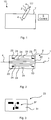
- Figure 1 is a schematic side-view in section of an embodiment of an electrical device 10, here in the form of a power transformer comprising a transformer tank, a control system 5 and a wound electrical component 1, here in the form of a bushing, passing through a wall of the electrical device 10.
- the bushing 1 comprises a wound body 2, e.g. a condenser core, of an electrically insulating material and is arranged to allow an electrical conductor 4, conducting a current I and voltage U, to pass through the wall 7.
- the conductor 4 also represents a central longitudinal axis 4 of the wound electrical component 1.
- the control system is arranged to i.a. control the current I passing through the wound electrical component 1, and thus, indirectly, control the temperature of said wound electrical component 1, heat being formed in the wound electrical component as a function of the current I and the resistance of the conductor 4.
- the electrical component 1 may be any electrical device comprising a wound body 2.
- the electrical component may be any of a bushing, e.g. transformer bushing, a transformer winding, a capacitor, a cable termination, a wound cable, machine insulation or an instrument transformer.
- Embodiments of the present invention may be especially useful for HV electrical devices 10, e.g. having a voltage rating within the range of 52-1100 kV.
- the wound electrical component 1 comprised in the electrical device may also have a voltage rating within the range of 52-1100 kV and thus configured for HV applications.
- Figure 2 illustrates a wound electrical component 1 in longitudinal section, e.g. a bushing as in figure 1 .
- the component 1 comprises a wound body 2 of an electrically insulating material 21.
- a conductor, representing a central longitudinal axis of the component as well as its wound body, 4 passes through a longitudinal through hole provided by a pipe 22 around which a web (e.g. a paper web or thermoplastic film) of the material 21 has been wound to form layers of the wound body 2.
- a web e.g. a paper web or thermoplastic film
- At least one, here a plurality of, one printed electronics sensors 23 are positioned inside the wound body 2, interleaved between layers of the body.
- At least one, here a plurality of, electrically conducting foils 24 are also positioned inside of the body, interleaved between layers of the body, to adjust/control the electrical field.
- conducting foils 24 conducting layers or electrodes corresponding to said foils may be provided in other ways than by interleaving foils.
- the conducting layers may e.g. be printed or painted on or between layers of the body.
- the at least one printed electronics sensor 23 comprises a plurality of printed electronics sensors 23, at different axial, and optionally radial, positions along the longitudinal axis 4.
- the sensors 23 may conveniently be positioned in the body 2 such that they are able to measure the temperatures of e.g. hotspots or temperature distribution within the body. Additionally or alternatively, the sensors 23 may conveniently be positioned in the body 2 such that they are able to communicate with the outside of the component 1, e.g. wirelessly, without interference from any electrically conducting foils 24.
- the electrically insulating material 21 is cellulose based, such as paper based, e.g. as Oil-Impregnated Paper, OIP, or Resin-Impregnated Paper, RIP, preferably epoxy impregnated paper, or based on a synthetic polymer. Layers of a paper may thus have been wound around the pipe 22 to form the wound body 2, after which the wound paper has been impregnated with e.g. oil, resin (e.g. epoxy) or any other electrically insulating, and optionally curable, fluid.
- the electrically insulating material may be a thermoplastic material, whereby the wound body 2 has been formed by winding and laminating a film of the thermoplastic material.
- the component 1 may be relatively large in size, especially if configured for HV applications, e.g. having a length within the range of from 30 cm to 10 or 20 m.
- Figure 3 schematically illustrates a printed electronics sensor 23 comprising or consisting of printed electronics circuits 32 printed onto a flexible substrate 31.
- the flexible substrate may be of a plastic or cellulose based material, e.g. paper, preferably a plastic material.
- the material of the substrate 31 should be resistant to the operating temperature of the component 1, and may thus preferably be a high temperature resistant plastic material.
- the substrate 31 is preferably a thin flexible film, e.g. having a thickness of at most 100 ⁇ m, e.g. less than 70 or 60 ⁇ m. In an embodiment, the substrate 31 has a thickness of about 50 ⁇ m (micrometres).
- the sensor may be connected by wiring and/or optical fibres.
- the printed circuits 32 may comprise a communication circuit for wireless communication and/or a power circuit for energy storage/supply to power the sensor, in addition to a temperature sensing circuit.
- the communication circuit may comprise a circuit in accordance with a Local Area Network (LAN) e.g. Wi-Fi, standard, or a Bluetooth, e.g. Bluetooth Low Energy (BLE) standard, and/or the communication circuit may comprise a circuit for a passive or active Radio-Frequency Identification (RFID) tag.
- LAN Local Area Network
- BLE Bluetooth Low Energy
- a passive RFID tag collect energy from a nearby RFID reader's interrogating radio waves.
- an active tag has a local power source (such as a battery).
- the power circuit may e.g. comprise a printed battery, printed onto the substrate 31, and/or the power circuit may comprise an energy harvesting circuit configured to generate electrical power from an electrical field formed when the wound electrical component 1 is used.
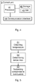
- FIG. 4 is a schematic block diagram of an embodiment of a control system 5 of the electrical device 10.
- the control system comprises processing circuitry 41 e.g. a central processing unit (CPU).
- the processing circuitry 41 may comprise one or a plurality of processing units in the form of microprocessor(s). However, other suitable devices with computing capabilities could be comprised in the processing circuitry 41, e.g. an application specific integrated circuit (ASIC), a field programmable gate array (FPGA) or a complex programmable logic device (CPLD).
- ASIC application specific integrated circuit
- FPGA field programmable gate array
- CPLD complex programmable logic device
- the processing circuitry 41 is configured to run one or several computer program(s) or software (SW) 43 stored in a data storage 42 of one or several storage unit(s) e.g. a memory.
- the storage unit is regarded as a computer readable means as discussed herein and may e.g. be in the form of a Random Access Memory (RAM), a Flash memory or other solid state memory, or a hard disk, or be a combination thereof.
- the processing circuitry 41 may also be configured to store data in the storage 42, as needed.
- the control system 5 may also comprise a wired or wireless communication interface 44 for e.g. sending control signals to other parts of the electrical device 10 for controlling the same, e.g. for controlling the current I through the wound component 1.
- the control system may control the electrical device 10 based on e.g. the temperatures measured by the printed sensors 23.
- the measured temperatures may give information usable for determining the life span or health of the wound electrical component 1, e.g. for when it is time to replace or service the component.
- real-time temperature measurements from the sensors 23 may give a more precise indication of the electrical current load which the component 1 may be subjected to at any time, which may be different from the standard (fixed, e.g. specified by the manufacturer) current rating of the component.
- the temperature measurements may be used for determining the maximum load (current) which is allowed, and this load may be above the rating of the component 1.
- other factors which may affect the temperature measured in the wound body 2 include ambient conditions, e.g.
- temperature sensors 23 for obtaining real-time temperature measurements of the body 2 may thus allow for dynamic loading of the component 1 based on said temperature measurements, rather than static loading based on the rating of the component. Since the rating is for security reasons made rather conservative, overloading of the component 1 may be enabled in a secure manner thanks to the temperature measurements during time periods when the measured temperature does not exceed a pre-set maximum temperature.
- control system 5 may be configured, by means of stored instructions, i.e. SW 43, to obtain a temperature from the at least one sensor 23, measured in real-time; determine that the temperature is below a predetermined maximum temperature of the wound body 2; and in response to said determination, subjecting the wound electrical component 1 to an electrical current I which is above a current rating of said wound electrical component.
- the control system 5 may be centrally located or distributed at a distance from the device 10, and/or co-located with the device.
- Figure 5 is a flow chart of an embodiment of a method of the present invention.
- the method is performed in an electrical device 10 as discussed herein, e.g. by the control system 5 thereof which may be co-located with and/or located some distance from the electrical component 1 and/or other parts of the electrical device 10, for enabling controlled overloading of the wound electrical component 1 comprised in the electrical device 10.
- the method comprises obtaining S1 a temperature from the at least one sensor 23, measured in real-time.
- the method also comprises determining S2 that the obtained Si temperature is below a predetermined maximum temperature of the wound body 2.
- the method also comprises, in response to said determination S2, subjecting S3 the wound electrical component 1 to an electrical current I which is above a current rating of said wound electrical component.
- Embodiments of the present invention may be conveniently implemented using one or more conventional general purpose or specialized digital computer 5, computing device, machine, or microprocessor, including one or more processors 41, memory and/or computer readable storage media 42 programmed according to the teachings of the present disclosure.
- Appropriate software 43 coding can readily be prepared by skilled programmers based on the teachings of the present disclosure, as will be apparent to those skilled in the software art.
- the present invention includes a computer program product 42 which is a non-transitory storage medium or computer readable medium (media) having instructions 43 stored thereon/in which can be used to program a computer 5 to perform any of the methods/processes of the present invention.
- the storage medium 42 can include, but is not limited to, any type of disk including floppy disks, optical discs, DVD, CD-ROMs, microdrive, and magneto-optical disks, ROMs, RAMs, EPROMs, EEPROMs, DRAMs, VRAMs, flash memory devices, magnetic or optical cards, nanosystems (including molecular memory ICs), or any type of media or device suitable for storing instructions and/or data 43.
Landscapes
- Physics & Mathematics (AREA)
- General Physics & Mathematics (AREA)
- Engineering & Computer Science (AREA)
- Power Engineering (AREA)
- Measuring Temperature Or Quantity Of Heat (AREA)
- Investigating Or Analyzing Materials By The Use Of Electric Means (AREA)
- Housings And Mounting Of Transformers (AREA)
Abstract
Description
- The present disclosure relates to a wound electrical component comprising a sensor.
- Temperature sensors are useful in high-voltage (HV) transformer bushings for condition monitoring to facilitate for prediction of maintenance intervals, prediction of product failures, and for dynamic thermal rating.
- State of the art for temperature sensors in HV products is e.g. silicon electronics temperature sensors in power transformers which are installed inside the transformer tank and connected via an optical fibre to the outside. Such sensor systems and their installation are relatively expensive and bulky and are not feasible for smaller/cheaper products like transformer bushings.
-
US 2016/370416 discloses a method of determining a reduction of remaining service lifetime, of an electrical device during a specific time period. The device to be tested may e.g. be a distribution transformer of an AC network. The system for determining remaining lifetime comprises temperature sensors connected to a temperature measurement device and a communications modem. The system can be implemented as printed circuit boards. -
US 2016/265978 discloses a sensor assembly for monitoring the temperature of an electrical device. The sensor assembly is positioned within a hollow core in a housing through a hole drilled through surrounding support material. - It is an objective of the present invention to provide an improved way of measuring a temperature, moisture level or other property of a wound electrical component.
- According to an aspect of the present invention, there is provided a wound electrical component comprising a wound body comprising a plurality of wound layers of an electrically insulating material around a longitudinal axis of the body, and at least one printed electronics sensor consisting of printed circuits on a flexible substrate. Each of the at least one sensor is interleaved between two of the wound layers. The electrical component is for instance a bushing, e.g. transformer bushing, a transformer winding, a capacitor, a cable termination, a wound cable, an instrument transformer, or a machine insulation. Preferably the electrical component is a HV transformer bushing.
- According to another aspect of the present invention, there is provided an electrical device comprising an embodiment of the wound electrical component of the present disclosure. The electrical device may e.g. be a transformer, e.g. a HV transformer, dry or liquid-filled, comprising the wound electrical component.
- According to another aspect of the present invention, there is provided a control system of an embodiment of the electrical device of the present disclosure. The control system comprises processing circuitry and a data storage storing instructions executable by said processing circuitry whereby said control system is operative to obtain a temperature from the at least one sensor, measured in real-time; determine that the temperature is below a predetermined maximum temperature of the wound body; and in response to said determination, subjecting the wound electrical component to an electrical current which is above a current rating of said wound electrical component. In addition, in some embodiments, temperature information from temperature sensor may also be used for scheduling maintenance and for predicting life span and risk of breakdown of the electrical component or device.
- According to another aspect of the present invention, there is provided a method of an embodiment of the electrical device of the present disclosure. The method is for controlled overloading of the wound electrical component comprised in the electrical device. The method comprises obtaining a temperature from the at least one sensor, measured in real-time. The method also comprises determining that the obtained temperature is below a predetermined maximum temperature of the wound body. The method also comprises, in response to said determination, subjecting the wound electrical component to an electrical current which is above a current rating of said wound electrical component.
- By using printed electronics for the sensors, e.g. temperature sensors, wherein the sensors are printed onto a flexible substrate, typically a thin flexible substrate of a plastic material, the sensors may be interleaved between layers of the wound body, somethings which would not be possible with conventional sensors mounted on a stiff circuit board. Further, printed sensors may be placed within electrical insulation without disturbing the electrical field. For instance, temperature measurements within e.g. a condenser core of a bushing is made possible.
- It is to be noted that any feature of any of the aspects may be applied to any other aspect, wherever appropriate. Likewise, any advantage of any of the aspects may apply to any of the other aspects. Other objectives, features and advantages of the enclosed embodiments will be apparent from the following detailed disclosure, from the attached dependent claims as well as from the drawings.
- Generally, all terms used in the claims are to be interpreted according to their ordinary meaning in the technical field, unless explicitly defined otherwise herein. All references to "a/an/the element, apparatus, component, means, step, etc." are to be interpreted openly as referring to at least one instance of the element, apparatus, component, means, step, etc., unless explicitly stated otherwise. The steps of any method disclosed herein do not have to be performed in the exact order disclosed, unless explicitly stated. The use of "first", "second" etc. for different features/components of the present disclosure are only intended to distinguish the features/components from other similar features/components and not to impart any order or hierarchy to the features/components.
- Embodiments will be described, by way of example, with reference to the accompanying drawings, in which:
-
Fig 1 is a schematic illustration of an embodiment of an electrical device comprising a wound electrical component, in accordance with the present invention. -
Fig 2 is a schematic illustration of an embodiment of a wound electrical component, in longitudinal section, , in accordance with the present invention. -
Fig 3 is a schematic illustration of an embodiment of a printed electronics sensor, in accordance with the present invention. -
Fig 4 is a schematic block diagram of an embodiment of a control system in accordance with the present invention. -
Fig 5 is a schematic flow chart of an embodiment of a method of the present invention. - Embodiments will now be described more fully hereinafter with reference to the accompanying drawings, in which certain embodiments are shown. However, other embodiments in many different forms are possible within the scope of the present disclosure. Rather, the following embodiments are provided by way of example so that this disclosure will be thorough and complete, and will fully convey the scope of the disclosure to those skilled in the art. Like numbers refer to like elements throughout the description.
- In accordance with embodiments of the present invention it is proposed to use printed electronics sensors in wound electrical components, e.g. HV transformer bushings. Herein, a temperature sensor, i.e. the printed electronics sensor comprises a temperature sensing circuit, is discussed as an example of a printed electronics sensor, but any of the printed electronics sensors may alternatively or additionally comprise any other sensor circuit, e.g. a moisture sensing circuit for measuring the moisture level within the wound body and/or an acoustic sensing circuit for measuring sound e.g. of partial electrical discharges within the wound body. For instance, a temperature sensing circuit, e.g. InFlect™ temperature sensor or other circuitry realized by e.g. inkjet printing on the flexible substrate e.g. based on resistance measurements. Additionally or alternatively, a moisture sensing circuit, e.g. based on resistance measurements such as InFlect™ moisture sensor or based on humidity sensitive polymer and capacitance measurements such as a fully printed flexible humidity sensor, may e.g. be used for detecting ageing of the electrically insulating material due to moisture uptake. Additionally or alternatively, an acoustic sensing circuit, e.g. based on piezo electric ink such as pressure sensors for printed blast dosimeters or other printed acoustic sensor, may be used e.g. for detection and/or localization of partial discharges. However, it is preferred that at least some of the at least one printed electronics sensor comprises a temperature sensing circuit for measuring a temperature in the wound body. Such sensors are available on the market and are cheaper than silicon based sensors. Thanks to their smaller thickness they could seamlessly match into the component geometry without disturbing the electric field distribution of the wound body. In addition, they could be installed in a standard production process in the shape of a plastic/paper film/tape without adding much extra work.
- The printed sensor may be combined with printed electronics radio communication components to transmit information. On the same film/tape there could be printed radio communication devices connected to or comprised in the sensor circuitry. The sensor could be axially placed in a high-temperature region inside the wound body, e.g. condenser core, and the communication device could be axially placed outside the wound body to avoid damping/shielding effects of the epoxy/foils for the radio communication. In addition to a sensor circuit, e.g. a temperature sensing circuit, also other printed electronics sensor circuit(s) may be used in addition to temperature sensing circuit, possibly arranged on the same substrates as the temperature sensing circuits. Such additional sensor circuit(s) may e.g. include a moisture sensing circuit.
-
Figure 1 is a schematic side-view in section of an embodiment of anelectrical device 10, here in the form of a power transformer comprising a transformer tank, acontrol system 5 and a woundelectrical component 1, here in the form of a bushing, passing through a wall of theelectrical device 10. Thebushing 1 comprises awound body 2, e.g. a condenser core, of an electrically insulating material and is arranged to allow anelectrical conductor 4, conducting a current I and voltage U, to pass through thewall 7. Herein, theconductor 4 also represents a centrallongitudinal axis 4 of the woundelectrical component 1. The control system is arranged to i.a. control the current I passing through the woundelectrical component 1, and thus, indirectly, control the temperature of said woundelectrical component 1, heat being formed in the wound electrical component as a function of the current I and the resistance of theconductor 4. - The
electrical component 1 may be any electrical device comprising awound body 2. For instance, the electrical component may be any of a bushing, e.g. transformer bushing, a transformer winding, a capacitor, a cable termination, a wound cable, machine insulation or an instrument transformer. Embodiments of the present invention may be especially useful for HVelectrical devices 10, e.g. having a voltage rating within the range of 52-1100 kV. Further, the woundelectrical component 1 comprised in the electrical device may also have a voltage rating within the range of 52-1100 kV and thus configured for HV applications. -
Figure 2 illustrates a woundelectrical component 1 in longitudinal section, e.g. a bushing as infigure 1 . Thecomponent 1 comprises awound body 2 of an electrically insulatingmaterial 21. A conductor, representing a central longitudinal axis of the component as well as its wound body, 4 passes through a longitudinal through hole provided by apipe 22 around which a web (e.g. a paper web or thermoplastic film) of thematerial 21 has been wound to form layers of thewound body 2. At least one, here a plurality of, one printedelectronics sensors 23 are positioned inside thewound body 2, interleaved between layers of the body. Optionally, depending on the type ofcomponent 1, at least one, here a plurality of, electrically conducting foils 24 are also positioned inside of the body, interleaved between layers of the body, to adjust/control the electrical field. As an alternative to conducting foils 24, conducting layers or electrodes corresponding to said foils may be provided in other ways than by interleaving foils. The conducting layers may e.g. be printed or painted on or between layers of the body. Preferably, the at least one printedelectronics sensor 23 comprises a plurality of printedelectronics sensors 23, at different axial, and optionally radial, positions along thelongitudinal axis 4. - The
sensors 23 may conveniently be positioned in thebody 2 such that they are able to measure the temperatures of e.g. hotspots or temperature distribution within the body. Additionally or alternatively, thesensors 23 may conveniently be positioned in thebody 2 such that they are able to communicate with the outside of thecomponent 1, e.g. wirelessly, without interference from any electrically conducting foils 24. - In some embodiments, the electrically insulating
material 21 is cellulose based, such as paper based, e.g. as Oil-Impregnated Paper, OIP, or Resin-Impregnated Paper, RIP, preferably epoxy impregnated paper, or based on a synthetic polymer. Layers of a paper may thus have been wound around thepipe 22 to form thewound body 2, after which the wound paper has been impregnated with e.g. oil, resin (e.g. epoxy) or any other electrically insulating, and optionally curable, fluid. Alternatively, the electrically insulating material may be a thermoplastic material, whereby thewound body 2 has been formed by winding and laminating a film of the thermoplastic material. - The
component 1 may be relatively large in size, especially if configured for HV applications, e.g. having a length within the range of from 30 cm to 10 or 20 m. -
Figure 3 schematically illustrates a printedelectronics sensor 23 comprising or consisting of printedelectronics circuits 32 printed onto aflexible substrate 31. - The flexible substrate may be of a plastic or cellulose based material, e.g. paper, preferably a plastic material. The material of the
substrate 31 should be resistant to the operating temperature of thecomponent 1, and may thus preferably be a high temperature resistant plastic material. To seamlessly integrate in the wound body, thesubstrate 31 is preferably a thin flexible film, e.g. having a thickness of at most 100 µm, e.g. less than 70 or 60 µm. In an embodiment, thesubstrate 31 has a thickness of about 50 µm (micrometres). - For communication with and/or for powering of each
sensor 23, the sensor may be connected by wiring and/or optical fibres. However, since thesensor 23 is integrated between layers of thewound body 2, it may not be convenient with such structural connections between the sensor and the outside of the body. Instead, the printedcircuits 32 may comprise a communication circuit for wireless communication and/or a power circuit for energy storage/supply to power the sensor, in addition to a temperature sensing circuit. The communication circuit may comprise a circuit in accordance with a Local Area Network (LAN) e.g. Wi-Fi, standard, or a Bluetooth, e.g. Bluetooth Low Energy (BLE) standard, and/or the communication circuit may comprise a circuit for a passive or active Radio-Frequency Identification (RFID) tag. A passive RFID tag collect energy from a nearby RFID reader's interrogating radio waves. In contrast, an active tag has a local power source (such as a battery). The power circuit may e.g. comprise a printed battery, printed onto thesubstrate 31, and/or the power circuit may comprise an energy harvesting circuit configured to generate electrical power from an electrical field formed when the woundelectrical component 1 is used. -
Figure 4 is a schematic block diagram of an embodiment of acontrol system 5 of theelectrical device 10. The control system comprises processingcircuitry 41 e.g. a central processing unit (CPU). Theprocessing circuitry 41 may comprise one or a plurality of processing units in the form of microprocessor(s). However, other suitable devices with computing capabilities could be comprised in theprocessing circuitry 41, e.g. an application specific integrated circuit (ASIC), a field programmable gate array (FPGA) or a complex programmable logic device (CPLD). Theprocessing circuitry 41 is configured to run one or several computer program(s) or software (SW) 43 stored in adata storage 42 of one or several storage unit(s) e.g. a memory. The storage unit is regarded as a computer readable means as discussed herein and may e.g. be in the form of a Random Access Memory (RAM), a Flash memory or other solid state memory, or a hard disk, or be a combination thereof. Theprocessing circuitry 41 may also be configured to store data in thestorage 42, as needed. Thecontrol system 5 may also comprise a wired orwireless communication interface 44 for e.g. sending control signals to other parts of theelectrical device 10 for controlling the same, e.g. for controlling the current I through thewound component 1. - The control system may control the
electrical device 10 based on e.g. the temperatures measured by the printedsensors 23. For instance, the measured temperatures may give information usable for determining the life span or health of the woundelectrical component 1, e.g. for when it is time to replace or service the component. Further, real-time temperature measurements from thesensors 23 may give a more precise indication of the electrical current load which thecomponent 1 may be subjected to at any time, which may be different from the standard (fixed, e.g. specified by the manufacturer) current rating of the component. Thus, the temperature measurements may be used for determining the maximum load (current) which is allowed, and this load may be above the rating of thecomponent 1. Apart from the current, other factors which may affect the temperature measured in thewound body 2 include ambient conditions, e.g. temperature, as well as heat dissipation in the electrically insulatingmaterial 21. The use oftemperature sensors 23 for obtaining real-time temperature measurements of thebody 2 may thus allow for dynamic loading of thecomponent 1 based on said temperature measurements, rather than static loading based on the rating of the component. Since the rating is for security reasons made rather conservative, overloading of thecomponent 1 may be enabled in a secure manner thanks to the temperature measurements during time periods when the measured temperature does not exceed a pre-set maximum temperature. - Thus, the
control system 5 may be configured, by means of stored instructions, i.e.SW 43, to obtain a temperature from the at least onesensor 23, measured in real-time; determine that the temperature is below a predetermined maximum temperature of thewound body 2; and in response to said determination, subjecting the woundelectrical component 1 to an electrical current I which is above a current rating of said wound electrical component. Thecontrol system 5 may be centrally located or distributed at a distance from thedevice 10, and/or co-located with the device. -
Figure 5 is a flow chart of an embodiment of a method of the present invention. The method is performed in anelectrical device 10 as discussed herein, e.g. by thecontrol system 5 thereof which may be co-located with and/or located some distance from theelectrical component 1 and/or other parts of theelectrical device 10, for enabling controlled overloading of the woundelectrical component 1 comprised in theelectrical device 10. The method comprises obtaining S1 a temperature from the at least onesensor 23, measured in real-time. The method also comprises determining S2 that the obtained Si temperature is below a predetermined maximum temperature of thewound body 2. The method also comprises, in response to said determination S2, subjecting S3 the woundelectrical component 1 to an electrical current I which is above a current rating of said wound electrical component. - Embodiments of the present invention may be conveniently implemented using one or more conventional general purpose or specialized
digital computer 5, computing device, machine, or microprocessor, including one ormore processors 41, memory and/or computerreadable storage media 42 programmed according to the teachings of the present disclosure.Appropriate software 43 coding can readily be prepared by skilled programmers based on the teachings of the present disclosure, as will be apparent to those skilled in the software art. - In some embodiments, the present invention includes a
computer program product 42 which is a non-transitory storage medium or computer readable medium (media) havinginstructions 43 stored thereon/in which can be used to program acomputer 5 to perform any of the methods/processes of the present invention. Examples of thestorage medium 42 can include, but is not limited to, any type of disk including floppy disks, optical discs, DVD, CD-ROMs, microdrive, and magneto-optical disks, ROMs, RAMs, EPROMs, EEPROMs, DRAMs, VRAMs, flash memory devices, magnetic or optical cards, nanosystems (including molecular memory ICs), or any type of media or device suitable for storing instructions and/ordata 43. - The present disclosure has mainly been described above with reference to a few embodiments. However, as is readily appreciated by a person skilled in the art, other embodiments than the ones disclosed above are equally possible within the scope of the present disclosure, as defined by the appended claims.
Claims (15)
- A wound electrical component (1) comprising:a wound body (2) comprising a plurality of wound layers of an electrically insulating material (21) around a longitudinal axis (4) of the body; andat least one printed electronics sensor (23) consisting of printed circuits (32) on a flexible substrate (31);wherein each of the at least one sensor is interleaved between two of the wound layers.
- The component of claim 1, wherein the printed circuits (32) comprise at least one of: a temperature sensing circuit, an acoustic sensing circuit and a moisture sensing circuit, preferably a temperature sensing circuit.
- The component of claim 1, wherein the printed circuits (32) comprise a circuit for wireless communication, e.g. in accordance with a Local Area Network, LAN, e.g. Wi-Fi, standard, or a Bluetooth, e.g. Bluetooth Low Energy, BLE, standard, or a passive or active Radio-Frequency Identification, RFID, tag.
- The component of any preceding claim, wherein the printed circuits (32) comprise an energy harvesting circuit configured to generate electrical power from an electrical field formed when the wound electrical component is used.
- The component of any preceding claim, wherein the wound electrical component (1) is configured for high-voltage, HV, applications, e.g. having a voltage rating within the range of 52-1100 kV.
- The component of any preceding claim, wherein the electrically insulating material (21) is cellulose based, such as paper based, e.g. as Oil-Impregnated Paper, OIP, or Resin-Impregnated Paper, RIP, preferably epoxy impregnated paper, or based on a synthetic polymer.
- The component of any preceding claim, wherein an electrically conducting foil (24) is interleaved between some of the wound layers of the wound body (2), or wherein conducting layers are printed or painted on some of the wound layers of the wound body (2).
- The component of any preceding claim, wherein the flexible substrate (31) is a film having a thickness of at most 100 µm, e.g. less than 70 or 60 µm.
- The component of any preceding claim, wherein the flexible substrate (31) is resistant to an operating temperature of the wound electrical component (1).
- The component of any preceding claim, wherein the flexible substrate (31) is of a plastic material.
- The component of any preceding claim, wherein the at least one printed electronics sensor comprises a plurality of printed electronics sensors (23), at different axial, and optionally radial, positions along the longitudinal axis (4).
- The component of any preceding claim, wherein the component (1) comprises a bushing, e.g. transformer bushing, a transformer winding, a capacitor, a cable termination, a wound cable, machine insulation or an instrument transformer, preferably a HV transformer bushing.
- An electrical device (10) comprising the wound electrical component (1) of any preceding claim.
- The electrical device (10) of claim 13, further comprising a control system (5) comprising processing circuitry (41) and a data storage (42) storing instructions (43) executable by said processing circuitry whereby said control system is operative to:obtain a temperature from the at least one sensor (23), measured in real-time;determine that the temperature is below a predetermined maximum temperature of the wound body (2); andin response to said determination, subjecting the wound electrical component (1) to an electrical current (I) which is above a current rating of said wound electrical component.
- A method of an electrical device (10) of claim 13 or 14, for controlled overloading of its wound electrical component (1), the method comprising:obtaining (S1) a temperature from the at least one sensor (23), measured in real-time;determining (S2) that the obtained (Si) temperature is below a predetermined maximum temperature of the wound body (2); andin response to said determination (S2), subjecting (S3) the wound electrical component (1) to an electrical current (I) which is above a current rating of said wound electrical component.
Priority Applications (5)
| Application Number | Priority Date | Filing Date | Title |
|---|---|---|---|
| EP18154327.3A EP3521786B8 (en) | 2018-01-31 | 2018-01-31 | Wound electrical component with printed electronics sensor |
| CN201980009558.7A CN111712695A (en) | 2018-01-31 | 2019-01-21 | Wound electrical components with printed electronic sensors |
| US16/962,092 US11137293B2 (en) | 2018-01-31 | 2019-01-21 | Wound electrical component with printed electronics sensor |
| PCT/EP2019/051358 WO2019149554A1 (en) | 2018-01-31 | 2019-01-21 | Wound electrical component with printed electronics sensor |
| KR1020207022249A KR102201014B1 (en) | 2018-01-31 | 2019-01-21 | Wire-wound electrical component with printed electronic sensor |
Applications Claiming Priority (1)
| Application Number | Priority Date | Filing Date | Title |
|---|---|---|---|
| EP18154327.3A EP3521786B8 (en) | 2018-01-31 | 2018-01-31 | Wound electrical component with printed electronics sensor |
Publications (3)
| Publication Number | Publication Date |
|---|---|
| EP3521786A1 true EP3521786A1 (en) | 2019-08-07 |
| EP3521786B1 EP3521786B1 (en) | 2020-10-07 |
| EP3521786B8 EP3521786B8 (en) | 2020-11-18 |
Family
ID=61132093
Family Applications (1)
| Application Number | Title | Priority Date | Filing Date |
|---|---|---|---|
| EP18154327.3A Active EP3521786B8 (en) | 2018-01-31 | 2018-01-31 | Wound electrical component with printed electronics sensor |
Country Status (5)
| Country | Link |
|---|---|
| US (1) | US11137293B2 (en) |
| EP (1) | EP3521786B8 (en) |
| KR (1) | KR102201014B1 (en) |
| CN (1) | CN111712695A (en) |
| WO (1) | WO2019149554A1 (en) |
Cited By (2)
| Publication number | Priority date | Publication date | Assignee | Title |
|---|---|---|---|---|
| WO2021063689A1 (en) * | 2019-09-30 | 2021-04-08 | Abb Power Grids Switzerland Ag | Curing investigating arrangement and method for controlling the curing of epoxy resin in the production of a high-voltage lead-through device |
| EP3828562A1 (en) * | 2019-11-28 | 2021-06-02 | ABB Power Grids Switzerland AG | Smart electrical bushing with integrated sensor |
Families Citing this family (2)
| Publication number | Priority date | Publication date | Assignee | Title |
|---|---|---|---|---|
| US11835392B2 (en) * | 2018-01-19 | 2023-12-05 | Hitachi Energy Ltd | Apparatus, system and method for temperature measurement for dry-type transformer |
| US11262247B1 (en) * | 2020-10-14 | 2022-03-01 | Cooper-Standard Automotive, Inc. | Fluid conduit with printed sensors |
Citations (3)
| Publication number | Priority date | Publication date | Assignee | Title |
|---|---|---|---|---|
| WO2015117823A1 (en) * | 2014-02-05 | 2015-08-13 | Abb Technology Ltd | Condenser core |
| US20160265978A1 (en) | 2015-03-10 | 2016-09-15 | Hubbell Incorporated | Temperature monitoring of high voltage distribution system components |
| US20160370416A1 (en) | 2014-10-27 | 2016-12-22 | Landis+Gyr (Europe) Ag | Method, system and assembly for determining a reduction of remaining service lifetime of an electrical device during a specific time period of operation of the electrical device |
Family Cites Families (14)
| Publication number | Priority date | Publication date | Assignee | Title |
|---|---|---|---|---|
| EP0825448A3 (en) | 1996-08-23 | 1999-12-29 | Asea Brown Boveri AG | Measuring device for a metal-encapsulated gas-insulated high voltage installation |
| JP3850311B2 (en) * | 2002-02-21 | 2006-11-29 | オムロン株式会社 | Remaining life prediction notification method and electronic device |
| US7421894B2 (en) * | 2005-07-14 | 2008-09-09 | Dale Keep | Sensors and associated methods, including surface condition sensors |
| DE102009007583A1 (en) * | 2009-02-02 | 2010-08-12 | Siemens Aktiengesellschaft | Arrangement with a dielectric between at least two conductive surfaces and passage for high voltages |
| NO330346B1 (en) * | 2009-07-20 | 2011-03-28 | Sinvent As | Local thermal management |
| KR20130128383A (en) | 2010-09-13 | 2013-11-26 | 피에스티 센서스 (피티와이) 리미티드 | Printed temperature sensor |
| EP2474986A1 (en) * | 2011-01-05 | 2012-07-11 | ABB Technology AG | Transformer coil |
| CN202678115U (en) * | 2011-12-27 | 2013-01-16 | 比亚迪股份有限公司 | Capacitor with safety early-warning function |
| US20140037956A1 (en) * | 2012-08-01 | 2014-02-06 | Umesh Kumar Sopory | High voltage high temperature heater cables, connectors, and insulations |
| US20140246929A1 (en) * | 2013-03-04 | 2014-09-04 | General Electric Company | High thermal conductivity insulation for electrical machines |
| CN104483995B (en) * | 2014-11-06 | 2016-09-28 | 深圳太辰光通信股份有限公司 | A kind of method adjusting transformator live load |
| EP3219010B1 (en) * | 2014-11-11 | 2020-07-08 | Maschinenfabrik Reinhausen GmbH | Resistor emulation and gate boost |
| KR101720237B1 (en) * | 2015-05-26 | 2017-04-10 | 주식회사 효성 | Bushing for condenser and making method of the same |
| CN106486221B (en) | 2016-11-24 | 2018-07-17 | 国网河南新密市供电公司 | A kind of insulating sleeve with temperature element and its application in the electrical apparatus |
-
2018
- 2018-01-31 EP EP18154327.3A patent/EP3521786B8/en active Active
-
2019
- 2019-01-21 KR KR1020207022249A patent/KR102201014B1/en active Active
- 2019-01-21 US US16/962,092 patent/US11137293B2/en active Active
- 2019-01-21 WO PCT/EP2019/051358 patent/WO2019149554A1/en not_active Ceased
- 2019-01-21 CN CN201980009558.7A patent/CN111712695A/en active Pending
Patent Citations (3)
| Publication number | Priority date | Publication date | Assignee | Title |
|---|---|---|---|---|
| WO2015117823A1 (en) * | 2014-02-05 | 2015-08-13 | Abb Technology Ltd | Condenser core |
| US20160370416A1 (en) | 2014-10-27 | 2016-12-22 | Landis+Gyr (Europe) Ag | Method, system and assembly for determining a reduction of remaining service lifetime of an electrical device during a specific time period of operation of the electrical device |
| US20160265978A1 (en) | 2015-03-10 | 2016-09-15 | Hubbell Incorporated | Temperature monitoring of high voltage distribution system components |
Cited By (3)
| Publication number | Priority date | Publication date | Assignee | Title |
|---|---|---|---|---|
| WO2021063689A1 (en) * | 2019-09-30 | 2021-04-08 | Abb Power Grids Switzerland Ag | Curing investigating arrangement and method for controlling the curing of epoxy resin in the production of a high-voltage lead-through device |
| EP3828562A1 (en) * | 2019-11-28 | 2021-06-02 | ABB Power Grids Switzerland AG | Smart electrical bushing with integrated sensor |
| WO2021105210A1 (en) * | 2019-11-28 | 2021-06-03 | Abb Power Grids Switzerland Ag | Smart electrical bushing with integrated sensor |
Also Published As
| Publication number | Publication date |
|---|---|
| EP3521786B8 (en) | 2020-11-18 |
| CN111712695A (en) | 2020-09-25 |
| KR102201014B1 (en) | 2021-01-11 |
| KR20200096313A (en) | 2020-08-11 |
| US20200378836A1 (en) | 2020-12-03 |
| WO2019149554A1 (en) | 2019-08-08 |
| EP3521786B1 (en) | 2020-10-07 |
| US11137293B2 (en) | 2021-10-05 |
Similar Documents
| Publication | Publication Date | Title |
|---|---|---|
| US11137293B2 (en) | Wound electrical component with printed electronics sensor | |
| US10254323B2 (en) | Passive wireless monitoring of individual capacitor cans | |
| US7990156B1 (en) | Method and apparatus for measuring degradation of insulation of electrical power system devices | |
| Madonna et al. | Evaluation of strand‐to‐strand capacitance and dissipation factor in thermally aged enamelled coils for low‐voltage electrical machines | |
| US20090167541A1 (en) | Monitoring of Capacitor | |
| WO2023107900A1 (en) | Electric power asset health monitoring | |
| EP3757526B1 (en) | Resonator array sensor arrangement | |
| US8434211B2 (en) | Method for manufacturing a capacitive measuring apparatus | |
| Chin et al. | Development of a Flexible Rogowski Coil Sensor for Partial Discharge Detection in Power Cables | |
| KR102297841B1 (en) | High-voltage read-through device and apparatus for handling data of high-voltage lead-through device | |
| CN112912722B (en) | Electrical apparatus provided with moisture sensor | |
| US11688214B1 (en) | Composite panel with a wireless, self-powered or remotely powered sensing assembly | |
| EP3828562B1 (en) | Smart electrical bushing with integrated sensor | |
| WO2021063689A1 (en) | Curing investigating arrangement and method for controlling the curing of epoxy resin in the production of a high-voltage lead-through device | |
| US20250216460A1 (en) | Sensor system for an electric machine | |
| US20230175954A1 (en) | Electric power asset health monitoring | |
| EP4476750A1 (en) | Electrical isolator | |
| Phung et al. | Acoustic monitoring of partial discharges using fibre optic sensors |
Legal Events
| Date | Code | Title | Description |
|---|---|---|---|
| PUAI | Public reference made under article 153(3) epc to a published international application that has entered the european phase |
Free format text: ORIGINAL CODE: 0009012 |
|
| STAA | Information on the status of an ep patent application or granted ep patent |
Free format text: STATUS: THE APPLICATION HAS BEEN PUBLISHED |
|
| AK | Designated contracting states |
Kind code of ref document: A1 Designated state(s): AL AT BE BG CH CY CZ DE DK EE ES FI FR GB GR HR HU IE IS IT LI LT LU LV MC MK MT NL NO PL PT RO RS SE SI SK SM TR |
|
| AX | Request for extension of the european patent |
Extension state: BA ME |
|
| STAA | Information on the status of an ep patent application or granted ep patent |
Free format text: STATUS: REQUEST FOR EXAMINATION WAS MADE |
|
| 17P | Request for examination filed |
Effective date: 20200206 |
|
| RBV | Designated contracting states (corrected) |
Designated state(s): AL AT BE BG CH CY CZ DE DK EE ES FI FR GB GR HR HU IE IS IT LI LT LU LV MC MK MT NL NO PL PT RO RS SE SI SK SM TR |
|
| GRAP | Despatch of communication of intention to grant a patent |
Free format text: ORIGINAL CODE: EPIDOSNIGR1 |
|
| STAA | Information on the status of an ep patent application or granted ep patent |
Free format text: STATUS: GRANT OF PATENT IS INTENDED |
|
| INTG | Intention to grant announced |
Effective date: 20200612 |
|
| GRAS | Grant fee paid |
Free format text: ORIGINAL CODE: EPIDOSNIGR3 |
|
| GRAA | (expected) grant |
Free format text: ORIGINAL CODE: 0009210 |
|
| STAA | Information on the status of an ep patent application or granted ep patent |
Free format text: STATUS: THE PATENT HAS BEEN GRANTED |
|
| AK | Designated contracting states |
Kind code of ref document: B1 Designated state(s): AL AT BE BG CH CY CZ DE DK EE ES FI FR GB GR HR HU IE IS IT LI LT LU LV MC MK MT NL NO PL PT RO RS SE SI SK SM TR |
|
| REG | Reference to a national code |
Ref country code: GB Ref legal event code: FG4D |
|
| REG | Reference to a national code |
Ref country code: AT Ref legal event code: REF Ref document number: 1321655 Country of ref document: AT Kind code of ref document: T Effective date: 20201015 Ref country code: CH Ref legal event code: EP |
|
| REG | Reference to a national code |
Ref country code: DE Ref legal event code: R081 Ref document number: 602018008356 Country of ref document: DE Owner name: HITACHI ENERGY SWITZERLAND AG, CH Free format text: FORMER OWNER: ABB SCHWEIZ AG, BADEN, CH Ref country code: DE Ref legal event code: R081 Ref document number: 602018008356 Country of ref document: DE Owner name: HITACHI ENERGY LTD, CH Free format text: FORMER OWNER: ABB SCHWEIZ AG, BADEN, CH |
|
| REG | Reference to a national code |
Ref country code: IE Ref legal event code: FG4D |
|
| REG | Reference to a national code |
Ref country code: DE Ref legal event code: R096 Ref document number: 602018008356 Country of ref document: DE |
|
| REG | Reference to a national code |
Ref country code: CH Ref legal event code: PK Free format text: BERICHTIGUNG B8 |
|
| RAP2 | Party data changed (patent owner data changed or rights of a patent transferred) |
Owner name: ABB POWER GRIDS SWITZERLAND AG |
|
| REG | Reference to a national code |
Ref country code: NL Ref legal event code: MP Effective date: 20201007 |
|
| REG | Reference to a national code |
Ref country code: AT Ref legal event code: MK05 Ref document number: 1321655 Country of ref document: AT Kind code of ref document: T Effective date: 20201007 |
|
| PG25 | Lapsed in a contracting state [announced via postgrant information from national office to epo] |
Ref country code: PT Free format text: LAPSE BECAUSE OF FAILURE TO SUBMIT A TRANSLATION OF THE DESCRIPTION OR TO PAY THE FEE WITHIN THE PRESCRIBED TIME-LIMIT Effective date: 20210208 Ref country code: RS Free format text: LAPSE BECAUSE OF FAILURE TO SUBMIT A TRANSLATION OF THE DESCRIPTION OR TO PAY THE FEE WITHIN THE PRESCRIBED TIME-LIMIT Effective date: 20201007 Ref country code: FI Free format text: LAPSE BECAUSE OF FAILURE TO SUBMIT A TRANSLATION OF THE DESCRIPTION OR TO PAY THE FEE WITHIN THE PRESCRIBED TIME-LIMIT Effective date: 20201007 Ref country code: GR Free format text: LAPSE BECAUSE OF FAILURE TO SUBMIT A TRANSLATION OF THE DESCRIPTION OR TO PAY THE FEE WITHIN THE PRESCRIBED TIME-LIMIT Effective date: 20210108 Ref country code: NO Free format text: LAPSE BECAUSE OF FAILURE TO SUBMIT A TRANSLATION OF THE DESCRIPTION OR TO PAY THE FEE WITHIN THE PRESCRIBED TIME-LIMIT Effective date: 20210107 |
|
| REG | Reference to a national code |
Ref country code: LT Ref legal event code: MG4D |
|
| PG25 | Lapsed in a contracting state [announced via postgrant information from national office to epo] |
Ref country code: SE Free format text: LAPSE BECAUSE OF FAILURE TO SUBMIT A TRANSLATION OF THE DESCRIPTION OR TO PAY THE FEE WITHIN THE PRESCRIBED TIME-LIMIT Effective date: 20201007 Ref country code: IS Free format text: LAPSE BECAUSE OF FAILURE TO SUBMIT A TRANSLATION OF THE DESCRIPTION OR TO PAY THE FEE WITHIN THE PRESCRIBED TIME-LIMIT Effective date: 20210207 Ref country code: LV Free format text: LAPSE BECAUSE OF FAILURE TO SUBMIT A TRANSLATION OF THE DESCRIPTION OR TO PAY THE FEE WITHIN THE PRESCRIBED TIME-LIMIT Effective date: 20201007 Ref country code: PL Free format text: LAPSE BECAUSE OF FAILURE TO SUBMIT A TRANSLATION OF THE DESCRIPTION OR TO PAY THE FEE WITHIN THE PRESCRIBED TIME-LIMIT Effective date: 20201007 Ref country code: BG Free format text: LAPSE BECAUSE OF FAILURE TO SUBMIT A TRANSLATION OF THE DESCRIPTION OR TO PAY THE FEE WITHIN THE PRESCRIBED TIME-LIMIT Effective date: 20210107 Ref country code: ES Free format text: LAPSE BECAUSE OF FAILURE TO SUBMIT A TRANSLATION OF THE DESCRIPTION OR TO PAY THE FEE WITHIN THE PRESCRIBED TIME-LIMIT Effective date: 20201007 Ref country code: AT Free format text: LAPSE BECAUSE OF FAILURE TO SUBMIT A TRANSLATION OF THE DESCRIPTION OR TO PAY THE FEE WITHIN THE PRESCRIBED TIME-LIMIT Effective date: 20201007 |
|
| PG25 | Lapsed in a contracting state [announced via postgrant information from national office to epo] |
Ref country code: NL Free format text: LAPSE BECAUSE OF FAILURE TO SUBMIT A TRANSLATION OF THE DESCRIPTION OR TO PAY THE FEE WITHIN THE PRESCRIBED TIME-LIMIT Effective date: 20201007 Ref country code: HR Free format text: LAPSE BECAUSE OF FAILURE TO SUBMIT A TRANSLATION OF THE DESCRIPTION OR TO PAY THE FEE WITHIN THE PRESCRIBED TIME-LIMIT Effective date: 20201007 |
|
| REG | Reference to a national code |
Ref country code: DE Ref legal event code: R097 Ref document number: 602018008356 Country of ref document: DE |
|
| PG25 | Lapsed in a contracting state [announced via postgrant information from national office to epo] |
Ref country code: RO Free format text: LAPSE BECAUSE OF FAILURE TO SUBMIT A TRANSLATION OF THE DESCRIPTION OR TO PAY THE FEE WITHIN THE PRESCRIBED TIME-LIMIT Effective date: 20201007 Ref country code: SK Free format text: LAPSE BECAUSE OF FAILURE TO SUBMIT A TRANSLATION OF THE DESCRIPTION OR TO PAY THE FEE WITHIN THE PRESCRIBED TIME-LIMIT Effective date: 20201007 Ref country code: SM Free format text: LAPSE BECAUSE OF FAILURE TO SUBMIT A TRANSLATION OF THE DESCRIPTION OR TO PAY THE FEE WITHIN THE PRESCRIBED TIME-LIMIT Effective date: 20201007 Ref country code: EE Free format text: LAPSE BECAUSE OF FAILURE TO SUBMIT A TRANSLATION OF THE DESCRIPTION OR TO PAY THE FEE WITHIN THE PRESCRIBED TIME-LIMIT Effective date: 20201007 Ref country code: CZ Free format text: LAPSE BECAUSE OF FAILURE TO SUBMIT A TRANSLATION OF THE DESCRIPTION OR TO PAY THE FEE WITHIN THE PRESCRIBED TIME-LIMIT Effective date: 20201007 Ref country code: LT Free format text: LAPSE BECAUSE OF FAILURE TO SUBMIT A TRANSLATION OF THE DESCRIPTION OR TO PAY THE FEE WITHIN THE PRESCRIBED TIME-LIMIT Effective date: 20201007 |
|
| PLBE | No opposition filed within time limit |
Free format text: ORIGINAL CODE: 0009261 |
|
| STAA | Information on the status of an ep patent application or granted ep patent |
Free format text: STATUS: NO OPPOSITION FILED WITHIN TIME LIMIT |
|
| PG25 | Lapsed in a contracting state [announced via postgrant information from national office to epo] |
Ref country code: MC Free format text: LAPSE BECAUSE OF FAILURE TO SUBMIT A TRANSLATION OF THE DESCRIPTION OR TO PAY THE FEE WITHIN THE PRESCRIBED TIME-LIMIT Effective date: 20201007 Ref country code: DK Free format text: LAPSE BECAUSE OF FAILURE TO SUBMIT A TRANSLATION OF THE DESCRIPTION OR TO PAY THE FEE WITHIN THE PRESCRIBED TIME-LIMIT Effective date: 20201007 |
|
| 26N | No opposition filed |
Effective date: 20210708 |
|
| PG25 | Lapsed in a contracting state [announced via postgrant information from national office to epo] |
Ref country code: LU Free format text: LAPSE BECAUSE OF NON-PAYMENT OF DUE FEES Effective date: 20210131 |
|
| REG | Reference to a national code |
Ref country code: BE Ref legal event code: MM Effective date: 20210131 |
|
| PG25 | Lapsed in a contracting state [announced via postgrant information from national office to epo] |
Ref country code: AL Free format text: LAPSE BECAUSE OF FAILURE TO SUBMIT A TRANSLATION OF THE DESCRIPTION OR TO PAY THE FEE WITHIN THE PRESCRIBED TIME-LIMIT Effective date: 20201007 |
|
| PG25 | Lapsed in a contracting state [announced via postgrant information from national office to epo] |
Ref country code: SI Free format text: LAPSE BECAUSE OF FAILURE TO SUBMIT A TRANSLATION OF THE DESCRIPTION OR TO PAY THE FEE WITHIN THE PRESCRIBED TIME-LIMIT Effective date: 20201007 |
|
| PG25 | Lapsed in a contracting state [announced via postgrant information from national office to epo] |
Ref country code: IE Free format text: LAPSE BECAUSE OF NON-PAYMENT OF DUE FEES Effective date: 20210131 |
|
| PG25 | Lapsed in a contracting state [announced via postgrant information from national office to epo] |
Ref country code: IS Free format text: LAPSE BECAUSE OF FAILURE TO SUBMIT A TRANSLATION OF THE DESCRIPTION OR TO PAY THE FEE WITHIN THE PRESCRIBED TIME-LIMIT Effective date: 20210207 |
|
| REG | Reference to a national code |
Ref country code: DE Ref legal event code: R081 Ref document number: 602018008356 Country of ref document: DE Owner name: HITACHI ENERGY SWITZERLAND AG, CH Free format text: FORMER OWNER: ABB POWER GRIDS SWITZERLAND AG, BADEN, CH Ref country code: DE Ref legal event code: R081 Ref document number: 602018008356 Country of ref document: DE Owner name: HITACHI ENERGY LTD, CH Free format text: FORMER OWNER: ABB POWER GRIDS SWITZERLAND AG, BADEN, CH |
|
| PG25 | Lapsed in a contracting state [announced via postgrant information from national office to epo] |
Ref country code: BE Free format text: LAPSE BECAUSE OF NON-PAYMENT OF DUE FEES Effective date: 20210131 |
|
| PG25 | Lapsed in a contracting state [announced via postgrant information from national office to epo] |
Ref country code: CY Free format text: LAPSE BECAUSE OF FAILURE TO SUBMIT A TRANSLATION OF THE DESCRIPTION OR TO PAY THE FEE WITHIN THE PRESCRIBED TIME-LIMIT Effective date: 20201007 |
|
| P01 | Opt-out of the competence of the unified patent court (upc) registered |
Effective date: 20230527 |
|
| PG25 | Lapsed in a contracting state [announced via postgrant information from national office to epo] |
Ref country code: HU Free format text: LAPSE BECAUSE OF FAILURE TO SUBMIT A TRANSLATION OF THE DESCRIPTION OR TO PAY THE FEE WITHIN THE PRESCRIBED TIME-LIMIT; INVALID AB INITIO Effective date: 20180131 |
|
| REG | Reference to a national code |
Ref country code: DE Ref legal event code: R082 Ref document number: 602018008356 Country of ref document: DE Representative=s name: DENNEMEYER & ASSOCIATES RECHTSANWALTSGESELLSCH, DE Ref country code: DE Ref legal event code: R082 Ref document number: 602018008356 Country of ref document: DE Representative=s name: DENNEMEYER & ASSOCIATES S.A., DE Ref country code: DE Ref legal event code: R081 Ref document number: 602018008356 Country of ref document: DE Owner name: HITACHI ENERGY LTD, CH Free format text: FORMER OWNER: HITACHI ENERGY SWITZERLAND AG, BADEN, CH |
|
| PG25 | Lapsed in a contracting state [announced via postgrant information from national office to epo] |
Ref country code: MK Free format text: LAPSE BECAUSE OF FAILURE TO SUBMIT A TRANSLATION OF THE DESCRIPTION OR TO PAY THE FEE WITHIN THE PRESCRIBED TIME-LIMIT Effective date: 20201007 |
|
| REG | Reference to a national code |
Ref country code: GB Ref legal event code: 732E Free format text: REGISTERED BETWEEN 20240718 AND 20240724 |
|
| PG25 | Lapsed in a contracting state [announced via postgrant information from national office to epo] |
Ref country code: MT Free format text: LAPSE BECAUSE OF FAILURE TO SUBMIT A TRANSLATION OF THE DESCRIPTION OR TO PAY THE FEE WITHIN THE PRESCRIBED TIME-LIMIT Effective date: 20201007 |
|
| REG | Reference to a national code |
Ref country code: DE Ref legal event code: R082 Ref document number: 602018008356 Country of ref document: DE Representative=s name: DENNEMEYER & ASSOCIATES RECHTSANWALTSGESELLSCH, DE |
|
| PG25 | Lapsed in a contracting state [announced via postgrant information from national office to epo] |
Ref country code: TR Free format text: LAPSE BECAUSE OF FAILURE TO SUBMIT A TRANSLATION OF THE DESCRIPTION OR TO PAY THE FEE WITHIN THE PRESCRIBED TIME-LIMIT Effective date: 20201007 |
|
| REG | Reference to a national code |
Ref country code: CH Ref legal event code: U11 Free format text: ST27 STATUS EVENT CODE: U-0-0-U10-U11 (AS PROVIDED BY THE NATIONAL OFFICE) Effective date: 20260201 |
|
| PGFP | Annual fee paid to national office [announced via postgrant information from national office to epo] |
Ref country code: GB Payment date: 20260123 Year of fee payment: 9 |
|
| PGFP | Annual fee paid to national office [announced via postgrant information from national office to epo] |
Ref country code: DE Payment date: 20260121 Year of fee payment: 9 |
|
| PGFP | Annual fee paid to national office [announced via postgrant information from national office to epo] |
Ref country code: IT Payment date: 20260126 Year of fee payment: 9 |
|
| PGFP | Annual fee paid to national office [announced via postgrant information from national office to epo] |
Ref country code: FR Payment date: 20260123 Year of fee payment: 9 |
|
| PGFP | Annual fee paid to national office [announced via postgrant information from national office to epo] |
Ref country code: CH Payment date: 20260201 Year of fee payment: 9 |