EP3520931A1 - Terahertz inspection for additively manufactured materials - Google Patents
Terahertz inspection for additively manufactured materials Download PDFInfo
- Publication number
- EP3520931A1 EP3520931A1 EP19154612.6A EP19154612A EP3520931A1 EP 3520931 A1 EP3520931 A1 EP 3520931A1 EP 19154612 A EP19154612 A EP 19154612A EP 3520931 A1 EP3520931 A1 EP 3520931A1
- Authority
- EP
- European Patent Office
- Prior art keywords
- terahertz
- additive manufacturing
- inspection device
- thz
- probe
- Prior art date
- Legal status (The legal status is an assumption and is not a legal conclusion. Google has not performed a legal analysis and makes no representation as to the accuracy of the status listed.)
- Granted
Links
Images






Classifications
-
- G—PHYSICS
- G01—MEASURING; TESTING
- G01N—INVESTIGATING OR ANALYSING MATERIALS BY DETERMINING THEIR CHEMICAL OR PHYSICAL PROPERTIES
- G01N21/00—Investigating or analysing materials by the use of optical means, i.e. using sub-millimetre waves, infrared, visible or ultraviolet light
- G01N21/01—Arrangements or apparatus for facilitating the optical investigation
-
- B—PERFORMING OPERATIONS; TRANSPORTING
- B22—CASTING; POWDER METALLURGY
- B22F—WORKING METALLIC POWDER; MANUFACTURE OF ARTICLES FROM METALLIC POWDER; MAKING METALLIC POWDER; APPARATUS OR DEVICES SPECIALLY ADAPTED FOR METALLIC POWDER
- B22F10/00—Additive manufacturing of workpieces or articles from metallic powder
- B22F10/10—Formation of a green body
- B22F10/18—Formation of a green body by mixing binder with metal in filament form, e.g. fused filament fabrication [FFF]
-
- B—PERFORMING OPERATIONS; TRANSPORTING
- B22—CASTING; POWDER METALLURGY
- B22F—WORKING METALLIC POWDER; MANUFACTURE OF ARTICLES FROM METALLIC POWDER; MAKING METALLIC POWDER; APPARATUS OR DEVICES SPECIALLY ADAPTED FOR METALLIC POWDER
- B22F10/00—Additive manufacturing of workpieces or articles from metallic powder
- B22F10/30—Process control
- B22F10/38—Process control to achieve specific product aspects, e.g. surface smoothness, density, porosity or hollow structures
-
- B—PERFORMING OPERATIONS; TRANSPORTING
- B22—CASTING; POWDER METALLURGY
- B22F—WORKING METALLIC POWDER; MANUFACTURE OF ARTICLES FROM METALLIC POWDER; MAKING METALLIC POWDER; APPARATUS OR DEVICES SPECIALLY ADAPTED FOR METALLIC POWDER
- B22F10/00—Additive manufacturing of workpieces or articles from metallic powder
- B22F10/80—Data acquisition or data processing
- B22F10/85—Data acquisition or data processing for controlling or regulating additive manufacturing processes
-
- B—PERFORMING OPERATIONS; TRANSPORTING
- B22—CASTING; POWDER METALLURGY
- B22F—WORKING METALLIC POWDER; MANUFACTURE OF ARTICLES FROM METALLIC POWDER; MAKING METALLIC POWDER; APPARATUS OR DEVICES SPECIALLY ADAPTED FOR METALLIC POWDER
- B22F12/00—Apparatus or devices specially adapted for additive manufacturing; Auxiliary means for additive manufacturing; Combinations of additive manufacturing apparatus or devices with other processing apparatus or devices
- B22F12/40—Radiation means
- B22F12/41—Radiation means characterised by the type, e.g. laser or electron beam
-
- B—PERFORMING OPERATIONS; TRANSPORTING
- B22—CASTING; POWDER METALLURGY
- B22F—WORKING METALLIC POWDER; MANUFACTURE OF ARTICLES FROM METALLIC POWDER; MAKING METALLIC POWDER; APPARATUS OR DEVICES SPECIALLY ADAPTED FOR METALLIC POWDER
- B22F12/00—Apparatus or devices specially adapted for additive manufacturing; Auxiliary means for additive manufacturing; Combinations of additive manufacturing apparatus or devices with other processing apparatus or devices
- B22F12/40—Radiation means
- B22F12/44—Radiation means characterised by the configuration of the radiation means
-
- B—PERFORMING OPERATIONS; TRANSPORTING
- B22—CASTING; POWDER METALLURGY
- B22F—WORKING METALLIC POWDER; MANUFACTURE OF ARTICLES FROM METALLIC POWDER; MAKING METALLIC POWDER; APPARATUS OR DEVICES SPECIALLY ADAPTED FOR METALLIC POWDER
- B22F12/00—Apparatus or devices specially adapted for additive manufacturing; Auxiliary means for additive manufacturing; Combinations of additive manufacturing apparatus or devices with other processing apparatus or devices
- B22F12/50—Means for feeding of material, e.g. heads
-
- B—PERFORMING OPERATIONS; TRANSPORTING
- B22—CASTING; POWDER METALLURGY
- B22F—WORKING METALLIC POWDER; MANUFACTURE OF ARTICLES FROM METALLIC POWDER; MAKING METALLIC POWDER; APPARATUS OR DEVICES SPECIALLY ADAPTED FOR METALLIC POWDER
- B22F12/00—Apparatus or devices specially adapted for additive manufacturing; Auxiliary means for additive manufacturing; Combinations of additive manufacturing apparatus or devices with other processing apparatus or devices
- B22F12/90—Means for process control, e.g. cameras or sensors
-
- B—PERFORMING OPERATIONS; TRANSPORTING
- B29—WORKING OF PLASTICS; WORKING OF SUBSTANCES IN A PLASTIC STATE IN GENERAL
- B29C—SHAPING OR JOINING OF PLASTICS; SHAPING OF MATERIAL IN A PLASTIC STATE, NOT OTHERWISE PROVIDED FOR; AFTER-TREATMENT OF THE SHAPED PRODUCTS, e.g. REPAIRING
- B29C64/00—Additive manufacturing, i.e. manufacturing of three-dimensional [3D] objects by additive deposition, additive agglomeration or additive layering, e.g. by 3D printing, stereolithography or selective laser sintering
- B29C64/10—Processes of additive manufacturing
- B29C64/141—Processes of additive manufacturing using only solid materials
- B29C64/153—Processes of additive manufacturing using only solid materials using layers of powder being selectively joined, e.g. by selective laser sintering or melting
-
- B—PERFORMING OPERATIONS; TRANSPORTING
- B29—WORKING OF PLASTICS; WORKING OF SUBSTANCES IN A PLASTIC STATE IN GENERAL
- B29C—SHAPING OR JOINING OF PLASTICS; SHAPING OF MATERIAL IN A PLASTIC STATE, NOT OTHERWISE PROVIDED FOR; AFTER-TREATMENT OF THE SHAPED PRODUCTS, e.g. REPAIRING
- B29C64/00—Additive manufacturing, i.e. manufacturing of three-dimensional [3D] objects by additive deposition, additive agglomeration or additive layering, e.g. by 3D printing, stereolithography or selective laser sintering
- B29C64/30—Auxiliary operations or equipment
-
- B—PERFORMING OPERATIONS; TRANSPORTING
- B29—WORKING OF PLASTICS; WORKING OF SUBSTANCES IN A PLASTIC STATE IN GENERAL
- B29C—SHAPING OR JOINING OF PLASTICS; SHAPING OF MATERIAL IN A PLASTIC STATE, NOT OTHERWISE PROVIDED FOR; AFTER-TREATMENT OF THE SHAPED PRODUCTS, e.g. REPAIRING
- B29C64/00—Additive manufacturing, i.e. manufacturing of three-dimensional [3D] objects by additive deposition, additive agglomeration or additive layering, e.g. by 3D printing, stereolithography or selective laser sintering
- B29C64/30—Auxiliary operations or equipment
- B29C64/386—Data acquisition or data processing for additive manufacturing
- B29C64/393—Data acquisition or data processing for additive manufacturing for controlling or regulating additive manufacturing processes
-
- B—PERFORMING OPERATIONS; TRANSPORTING
- B33—ADDITIVE MANUFACTURING TECHNOLOGY
- B33Y—ADDITIVE MANUFACTURING, i.e. MANUFACTURING OF THREE-DIMENSIONAL [3D] OBJECTS BY ADDITIVE DEPOSITION, ADDITIVE AGGLOMERATION OR ADDITIVE LAYERING, e.g. BY 3D PRINTING, STEREOLITHOGRAPHY OR SELECTIVE LASER SINTERING
- B33Y10/00—Processes of additive manufacturing
-
- B—PERFORMING OPERATIONS; TRANSPORTING
- B33—ADDITIVE MANUFACTURING TECHNOLOGY
- B33Y—ADDITIVE MANUFACTURING, i.e. MANUFACTURING OF THREE-DIMENSIONAL [3D] OBJECTS BY ADDITIVE DEPOSITION, ADDITIVE AGGLOMERATION OR ADDITIVE LAYERING, e.g. BY 3D PRINTING, STEREOLITHOGRAPHY OR SELECTIVE LASER SINTERING
- B33Y30/00—Apparatus for additive manufacturing; Details thereof or accessories therefor
-
- B—PERFORMING OPERATIONS; TRANSPORTING
- B33—ADDITIVE MANUFACTURING TECHNOLOGY
- B33Y—ADDITIVE MANUFACTURING, i.e. MANUFACTURING OF THREE-DIMENSIONAL [3D] OBJECTS BY ADDITIVE DEPOSITION, ADDITIVE AGGLOMERATION OR ADDITIVE LAYERING, e.g. BY 3D PRINTING, STEREOLITHOGRAPHY OR SELECTIVE LASER SINTERING
- B33Y40/00—Auxiliary operations or equipment, e.g. for material handling
-
- B—PERFORMING OPERATIONS; TRANSPORTING
- B33—ADDITIVE MANUFACTURING TECHNOLOGY
- B33Y—ADDITIVE MANUFACTURING, i.e. MANUFACTURING OF THREE-DIMENSIONAL [3D] OBJECTS BY ADDITIVE DEPOSITION, ADDITIVE AGGLOMERATION OR ADDITIVE LAYERING, e.g. BY 3D PRINTING, STEREOLITHOGRAPHY OR SELECTIVE LASER SINTERING
- B33Y50/00—Data acquisition or data processing for additive manufacturing
-
- G—PHYSICS
- G01—MEASURING; TESTING
- G01N—INVESTIGATING OR ANALYSING MATERIALS BY DETERMINING THEIR CHEMICAL OR PHYSICAL PROPERTIES
- G01N21/00—Investigating or analysing materials by the use of optical means, i.e. using sub-millimetre waves, infrared, visible or ultraviolet light
- G01N21/17—Systems in which incident light is modified in accordance with the properties of the material investigated
- G01N21/25—Colour; Spectral properties, i.e. comparison of effect of material on the light at two or more different wavelengths or wavelength bands
- G01N21/31—Investigating relative effect of material at wavelengths characteristic of specific elements or molecules, e.g. atomic absorption spectrometry
- G01N21/35—Investigating relative effect of material at wavelengths characteristic of specific elements or molecules, e.g. atomic absorption spectrometry using infrared light
- G01N21/3563—Investigating relative effect of material at wavelengths characteristic of specific elements or molecules, e.g. atomic absorption spectrometry using infrared light for analysing solids; Preparation of samples therefor
-
- G—PHYSICS
- G01—MEASURING; TESTING
- G01N—INVESTIGATING OR ANALYSING MATERIALS BY DETERMINING THEIR CHEMICAL OR PHYSICAL PROPERTIES
- G01N21/00—Investigating or analysing materials by the use of optical means, i.e. using sub-millimetre waves, infrared, visible or ultraviolet light
- G01N21/17—Systems in which incident light is modified in accordance with the properties of the material investigated
- G01N21/25—Colour; Spectral properties, i.e. comparison of effect of material on the light at two or more different wavelengths or wavelength bands
- G01N21/31—Investigating relative effect of material at wavelengths characteristic of specific elements or molecules, e.g. atomic absorption spectrometry
- G01N21/35—Investigating relative effect of material at wavelengths characteristic of specific elements or molecules, e.g. atomic absorption spectrometry using infrared light
- G01N21/3581—Investigating relative effect of material at wavelengths characteristic of specific elements or molecules, e.g. atomic absorption spectrometry using infrared light using far infrared light; using Terahertz radiation
-
- B—PERFORMING OPERATIONS; TRANSPORTING
- B22—CASTING; POWDER METALLURGY
- B22F—WORKING METALLIC POWDER; MANUFACTURE OF ARTICLES FROM METALLIC POWDER; MAKING METALLIC POWDER; APPARATUS OR DEVICES SPECIALLY ADAPTED FOR METALLIC POWDER
- B22F10/00—Additive manufacturing of workpieces or articles from metallic powder
- B22F10/20—Direct sintering or melting
- B22F10/25—Direct deposition of metal particles, e.g. direct metal deposition [DMD] or laser engineered net shaping [LENS]
-
- B—PERFORMING OPERATIONS; TRANSPORTING
- B22—CASTING; POWDER METALLURGY
- B22F—WORKING METALLIC POWDER; MANUFACTURE OF ARTICLES FROM METALLIC POWDER; MAKING METALLIC POWDER; APPARATUS OR DEVICES SPECIALLY ADAPTED FOR METALLIC POWDER
- B22F10/00—Additive manufacturing of workpieces or articles from metallic powder
- B22F10/20—Direct sintering or melting
- B22F10/28—Powder bed fusion, e.g. selective laser melting [SLM] or electron beam melting [EBM]
-
- B—PERFORMING OPERATIONS; TRANSPORTING
- B29—WORKING OF PLASTICS; WORKING OF SUBSTANCES IN A PLASTIC STATE IN GENERAL
- B29C—SHAPING OR JOINING OF PLASTICS; SHAPING OF MATERIAL IN A PLASTIC STATE, NOT OTHERWISE PROVIDED FOR; AFTER-TREATMENT OF THE SHAPED PRODUCTS, e.g. REPAIRING
- B29C64/00—Additive manufacturing, i.e. manufacturing of three-dimensional [3D] objects by additive deposition, additive agglomeration or additive layering, e.g. by 3D printing, stereolithography or selective laser sintering
- B29C64/30—Auxiliary operations or equipment
- B29C64/386—Data acquisition or data processing for additive manufacturing
-
- B—PERFORMING OPERATIONS; TRANSPORTING
- B33—ADDITIVE MANUFACTURING TECHNOLOGY
- B33Y—ADDITIVE MANUFACTURING, i.e. MANUFACTURING OF THREE-DIMENSIONAL [3D] OBJECTS BY ADDITIVE DEPOSITION, ADDITIVE AGGLOMERATION OR ADDITIVE LAYERING, e.g. BY 3D PRINTING, STEREOLITHOGRAPHY OR SELECTIVE LASER SINTERING
- B33Y50/00—Data acquisition or data processing for additive manufacturing
- B33Y50/02—Data acquisition or data processing for additive manufacturing for controlling or regulating additive manufacturing processes
-
- G—PHYSICS
- G01—MEASURING; TESTING
- G01N—INVESTIGATING OR ANALYSING MATERIALS BY DETERMINING THEIR CHEMICAL OR PHYSICAL PROPERTIES
- G01N21/00—Investigating or analysing materials by the use of optical means, i.e. using sub-millimetre waves, infrared, visible or ultraviolet light
- G01N21/01—Arrangements or apparatus for facilitating the optical investigation
- G01N2021/0106—General arrangement of respective parts
- G01N2021/0112—Apparatus in one mechanical, optical or electronic block
-
- Y—GENERAL TAGGING OF NEW TECHNOLOGICAL DEVELOPMENTS; GENERAL TAGGING OF CROSS-SECTIONAL TECHNOLOGIES SPANNING OVER SEVERAL SECTIONS OF THE IPC; TECHNICAL SUBJECTS COVERED BY FORMER USPC CROSS-REFERENCE ART COLLECTIONS [XRACs] AND DIGESTS
- Y02—TECHNOLOGIES OR APPLICATIONS FOR MITIGATION OR ADAPTATION AGAINST CLIMATE CHANGE
- Y02P—CLIMATE CHANGE MITIGATION TECHNOLOGIES IN THE PRODUCTION OR PROCESSING OF GOODS
- Y02P10/00—Technologies related to metal processing
- Y02P10/25—Process efficiency
Definitions
- the present disclosure relates generally to non-destructive testing methods. More specifically, the present disclosure relates to the use of Terahertz frequencies to non-destructively inspect manufactured parts.
- additive manufacturing is the broad term encompassing computer assisted 3-D printing techniques.
- 3-D printing originally referred to a process that deposits a binder material onto a powder bed with inkjet printer heads layer-by-layer. More recently, the term is being used in popular vernacular to encompass a wider variety of additive manufacturing techniques. United States and global technical standards use the term "additive manufacturing” in this broader sense to connote manufacturing systems for producing three-dimensional (equivalently referred to herein as "3D") parts that are typically first fashioned digitally on a computer.
- standard ISO/ASTM52900-15 defines seven categories of AM processes within its meaning: binder jetting, directed energy deposition, material extrusion, material jetting, powder bed fusion, sheet lamination and vat photopolymerization.
- additive manufacturing has progressed to allow for layer-by-layer deposition of various materials.
- additive manufacturing has proven useful in the manufacture of one-off parts including, for example, parts used as prototypes, or other customized parts that may or may not lead to mass production.
- the use of additive manufacturing techniques to make certain parts e.g., load-bearing or structural parts
- the lack of accepted inspection techniques for additively manufactured parts, including additively manufactured parts used as load-bearing parts or other structural parts e.g., additively manufactured parts requiring inspection and certification
- apparatuses, systems and methods are presented for the non-destructive inspection of additively manufactured parts in real time during manufacture of the parts using radiation in the Terahertz frequency range.
- the present disclosure is directed to an apparatus comprising an additive manufacturing device including a material deposition head configured to form an additively-manufactured build, with the build comprising individual layers of deposited material, and with the additive manufacturing device comprising a deposition head, and a terahertz inspection device located proximate to the material deposition head.
- the terahertz inspection device includes a terahertz probe, and further includes a thermal shield that substantially envelops the terahertz probe.
- the present disclosure is directed to a system including a housing, an additive manufacturing device including a material deposition head located within the housing, with the material deposition head configured to deposit a plurality of successive material layers to form an additively manufactured part.
- the system further comprises a terahertz inspection device including a terahertz probe, with the probe located within the housing and with the probe located proximate to the material deposition head.
- the probe further includes a thermal shield substantially enveloping the probe.
- the terahertz inspection system is configured to non-destructively inspect at least one material layer in substantially real time during the deposit of the at least one material layer.
- the present disclosure is directed to a method for additively manufacturing a part, the method comprising individually depositing a plurality of material layers from a material deposition head of an additive manufacturing device to form a part. At least one of the individually deposited material layers are non-destructively inspected using terahertz energy.
- the method further comprises directing terahertz energy from a terahertz inspection device to a location on or within at least one material layer and receiving terahertz energy from at least one material layer and detecting characteristics of the at least one material layer being non-destructively inspected.
- a method further comprising orienting the terahertz inspection device proximate to the material deposition head and depositing at least one material layer at a temperature ranging from about 300F to about 450F. Substantially concurrently with the depositing of the plurality of material layers, at least one material layer is non-destructively inspected in real time and the terahertz inspection device is substantially enveloped in a thermal shield.
- Another aspect of the present disclosure is directed to a structural component for a vehicle, including an aircraft, made and inspected according to methods disclosed herein, and an aircraft comprising structural components made and inspected according to methods disclosed herein.
- the present disclosure is directed to apparatuses, systems and methods for non-destructively inspecting additively manufactured parts in real time using terahertz (referred to equivalently herein as "THz”) frequencies delivered from a THz probe positioned proximate to the additive manufacturing material deposition head, with the THz probe housed within a thermal shield encasing, or substantially enveloping, the THz probe.
- THz terahertz
- the THz frequency range refers to electromagnetic waves with frequencies between about 100 GHz and about 10 THz, or wavelengths between about 3 mm and about 30 ⁇ m existing in the radiation spectrum between the microwave and infrared regions.
- the present disclosure uses the terms "THz radiation”, “THz energy”, and “THz waves” equivalently.
- Terahertz waves pass through a variety of amorphous and opaque materials with high chemical selectivity, with the ability to image such material under THz interrogation with high definition.
- non-destructive THz inspection techniques for interrogating dielectric (e.g., non-conducting) materials includes the inspection of composite materials.
- AM processes or “3D manufacturing” processes progressively deposit extremely thin layers of material to create a 3D object from a computer assisted drawing (CAD) file or file formats that include Additive Manufacturing file (AMF) format.
- CAD computer assisted drawing
- AMF Additive Manufacturing file
- Additive manufacturing (AM) is presently understood as referring to processes used to create a three-dimensional (3D) object where layers of material are formed, typically under computer control, to create a manufactured object.
- Manufactured objects can be of almost any shape or geometry and are produced using digital model data from a 3D model or another electronic data source such as an AMF format.
- 3D printing or AM builds a three-dimensional object from a computer-aided design (CAD) model or an AMF or STL file format by successively adding material layer-by-layer to accurately produce a part having a desired and/or predetermined dimension and/or geometry.
- CAD computer-aided design
- aspects of the present invention contemplate the use of AM apparatuses, systems and processes to form an AM product (e.g., a part).
- a non-exhaustive list of such processes includes, without limitation, direct energy deposition; direct metal laser sintering; direct metal printing; electron beam additive manufacturing; electron beam melting; electron beam powder bed manufacturing; fused deposition modeling; fused filament fabrication; indirect powder bed manufacturing; laser cladding; laser deposition manufacturing; laser deposition welding; laser deposition welding/integrated milling; laser engineering net shaping; laser freeform manufacturing; laser metal deposition with powder; laser metal deposition with wire; laser powder bed manufacturing; laser puddle deposition; laser repair manufacturing; powder directed energy deposition; stereolithography; selective laser melting; selective laser sintering; small puddle deposition; or combinations thereof.
- FFF fused filament fabrication
- FDM fused deposition modeling
- a filament of thermoplastic material, or metal in the form of metal wire, or other material is fed into an extrusion nozzle head (e.g., a 3D printer extruder, or printer extruder head hereinafter equivalently referred to as a "printer head"), that heats the material and produces a deposit material flow.
- extrusion nozzle head e.g., a 3D printer extruder, or printer extruder head hereinafter equivalently referred to as a "printer head
- Another technique fuses parts of the layer and then moves "upward” in the working area, adding successive layers of material, and repeating the process until the piece has "built up” or formed a "build".
- This process uses the unfused media to support overhangs and thin walls in the part being produced, reducing the need for temporary auxiliary supports for the piece.
- the printing head is moved, under computer control to define a desired build of desired 3D dimensions.
- the printer head deposits layers while moving in two dimensions to deposit one horizontal layer at a time before the printer head is directed to a position that is slightly "upward" (e.g., upward from the previously deposited layer) before depositing a subsequent layer onto the build.
- the speed of the deposition through the print head and the movement of the print head can be controlled to interrupt and re-start material deposition to form a defined interrupted region within a deposited layer.
- Laser sintering techniques include, without limitation, selective laser sintering with both metals and polymers, and direct metal laser sintering.
- Selective laser melting does not use sintering for the fusion of powder granules, but will completely melt the powder using a high-energy laser to create fully dense materials in a layer-wise deposition method that has mechanical properties similar to those of conventional manufactured metals.
- Electron beam melting is a similar type of additive manufacturing technology for metal parts (e.g. titanium, titanium alloys).
- EBM manufactures parts by melting metal powder layer by layer with an electron beam in a high vacuum.
- Another method consists of an inkjet 3D printing system that creates the part one layer at a time by spreading a layer of powder (plaster or resins) and printing a binder in the cross-section of the part using an inkjet-like process.
- a layer of powder plaster or resins
- a binder in the cross-section of the part using an inkjet-like process.
- Photopolymerization is primarily used in stereolithography to produce a solid part from a liquid.
- Inkjet printer systems like the Objet PolyJet system spray photopolymer materials onto a build tray in ultra-thin layers (e.g., between 16 ⁇ m and 30 ⁇ m) until the part is completed.
- ultra-thin layers e.g., between 16 ⁇ m and 30 ⁇ m
- Each photopolymer layer is cured with UV light after it is jetted, producing fully cured models that can be handled and used without post-curing.
- ultrasmall features can be made with the 3D micro-fabrication technique used in multiphoton photopolymerization.
- a gel is cured to a solid only in the places where the laser was focused while the remaining gel is removed.
- Feature sizes of less than about 100 nm can be produced, as well as complex structures that can comprise moving and interlocked parts.
- Yet another approach uses a synthetic resin that is solidified using LEDs.
- Mask-image-projection-based stereolithography a 3D digital model is sliced by a set of horizontal planes. Each slice is converted into a two-dimensional mask image. The mask image is then projected onto a photocurable liquid resin surface and light is projected onto the resin to cure it in the shape of the layer.
- Continuous liquid interface production begins with a reservoir of liquid photopolymer resin. Part of the reservoir is transparent to ultraviolet light, causing the resin to solidify.
- powder-fed directed-energy deposition a high-power laser is used to melt metal powder supplied to the focus of the laser beam.
- the powder fed directed energy process is similar to Selective Laser Sintering, but the metal powder is applied only where material is being added to the part at that moment.
- aspects of the present disclosure contemplate the use of FFF and FDM processes, although any of the aforementioned deposition techniques and processes are contemplated.
- Exemplary FFF and FDM apparatuses used in the contemplated AM processes to manufacture the desire builds include systems capable of depositing material at temperatures up to about 428F, depending on the desired mechanical properties of the build.
- deposition rates of the deposited layers is controlled to effect a deposition rate ranging from about 4 to about 6 inches/sec.
- thermoplastics such as acrylonitrile butadiene styrene (ABS), polyacetic acid, high-impact polystyrene, thermoplastic polyurethane, aliphatic polyamides, polyether ether ketones (PEEKs), as well as composite materials, including ceramics.
- ABS acrylonitrile butadiene styrene
- PEEKs polyether ether ketones
- the additive manufacturing and substantially simultaneous THz inspection of deposited layers of composite and other materials including, without limitation, layers deposited via additive manufacturing processes comprising carbon fiber resin materials.
- carbon fiber resin materials supplied to an additive manufacturing device and system include materials supplied as feedstock, for example, in the form of neat resin further comprising fiber particulate material.
- representative resin materials for use to incorporate carbon fibers and fiber glass-incorporated material systems include, without limitation and for example, ULTEM 9085, polyetherketoneketone (PEKK), polycarbonate-ABS, polycarbonate, Vero, digital-ABS Plus, FDM Nylon 6; FDM nylon 12 CF; DFM Nylon 12; ULTEM 1010 (Stratasys, Ltd.); PPSF Model (Stratasys, Ltd.) etc.
- THz radiation is emitted from the customized THz inspection device, referred to equivalently herein as a "THz probe", or a THz inspection head".
- the THz probe is used in conjunction with an additive manufacturing system to non-destructively evaluate AM parts, by inspecting an individual deposited layer or layers in situ, and substantially in real time.
- the apparatuses, systems and methods of the present disclosure identify abnormalities in the AM parts as the parts are being fabricated, (e.g., during material deposition of each or selected layers, and therefore before completion of the entire part). That is, the THz inspection device is configured to inspect at least one individual layer of deposited material in substantially real time during material deposition.
- the term "substantially in real time” connote a time duration that approximates the time required to deposit a layer from an AM device print head to a build.
- the precise quantifiable amount of time required to deposit such a layer is dependent on the dimensions of the part being built, as well as many other deposition and manufacturing parameters.
- the aspects of the present disclosure contemplate an inspection, via THz radiation, of an individual layer (or desired number of layers of an AM build) occurring substantially concurrently with the depositing of the individual layer or layers of a build.
- the apparatuses and systems disclosed herein comprise a thermal shield configured to house and substantially envelop the THz probe.
- the THz probe is oriented proximate to the additive manufacturing material deposition device and head within an additive manufacturing chamber or housing.
- the additive manufacturing chamber operates at an elevated temperature as successive material layers are deposited.
- the material layers are deposited at a temperature ranging from about 300°F to about 450°F. and more particularly ranging from about 300°F to about 428°F.
- non-destructive THz inspection of at least one of the material layers is conducted substantially in situ and substantially in real time.
- Sensitive inspection instrumentation can be adversely impacted by significantly elevated temperature environments. This has limited the technology available to non-destructively inspect parts, requiring a delay of the inspection until part manufacturing has been completed.
- at least one non-destructive inspection device in the form of at least one THz probe is oriented in situ proximate to the deposition head of an additive manufacturing device while the device operates in an elevated temperature environment (e.g., ranging from about 300°F to about 450°F), with the THz probe encased or substantially enveloped in a protective thermal shield.
- the real time inspection of incremental deposited layers of additively manufactured parts using a THz inspection device positioned proximate to the material deposition head facilitates the inspection of an additively manufactured part during a build.
- the apparatuses, systems, and methods of the present disclosure enable the substantially real time detection of anomalies in an AM layer or layers during the build. In this way, such anomalies can be addressed much sooner in the manufacturing process.
- FIGs. 1A, 1B, and 1C are schematic representations of stages of an AM process according to aspects of the present disclosure that are utilized to form a part 16.
- a first stage 10a of an additive manufacturing material deposition process includes a material deposition head 11 oriented proximate to a THz probe 12, with the material deposition head 11 shown depositing a build 13.
- the build 13 comprises successively deposited individual material layers 13a.
- a (fourth) partially deposited material layer 14a is being deposited and incorporated into the build 13.
- FIG. 1B shows a second stage 10b of the process, where the (fourth) partially deposited material layer 14a has now been fully deposited to become a completed deposited material layer 14b included in the build 13.
- FIG. 1C shows a third stage 10c of the process where a subsequent material layer 15 is being deposited onto material layer 14b, and is adding a layer to the build 13. In operation, material layers are continually added to the build 13 until the part 16 is completed.
- the material deposition head 11 is oriented proximate to, and at a predetermined distance from the THz probe. According to an aspect of the present disclosure, the deposition head is oriented at a distance from the THz probe ranging from about 0.5" to about 2.0".
- FIG. 2 is a cross-sectional view of a monostatic THz probe 22 showing the THz probe 22 substantially enveloped or encased within a thermal shield 26.
- Monostatic THZ probe 22 is shown in communication with a fiber optic cable 28, although any suitable connection for a THz probe is presently contemplated.
- Monostatic THz probe 22 further comprises a THz emitter/receiver 24 in communication with fiber optic cable 28. During operation, the THz radiation proceeds from the THz emitter/receiver 24 in the direction of lens 27, and proceeds from the monostatic THz probe 22 to a targeted region of a substrate toward which the monostatic THz probe 22 is directed.
- the emitter/receiver 24 and the lens 27 are constructed or otherwise selected to set a focus and to refract radiation to a predetermined distance from the emitter/receiver 24.
- data is captured by the emitter/receiver 24 as raw waveforms of the THz reflections from the target (not shown in FIG. 2 ).
- the inspected target can be a build layer surface or build layer subsurface. According to present aspects, individual build layers can be deposited at average thicknesses ranging from about 0.005" to about 0.020" thick.
- the outer surface of monostatic THz probe 22 is encased or otherwise substantially enveloped by thermal shield 26.
- the monostatic THz probe 22 accomplishes both the transmission and receiving functions in a single unit.
- the thermal shield 26 will not interfere with the monostatic THz probe's ability to emit THz radiation from the probe.
- the terms "encased”, “substantially encased” and “substantially enveloped” refer to a state where the thermal shield 26 encases or surrounds a predominant portion of the monostatic THz probe 22 to an extent where the probe is able to operate in an elevated temperature environment ranging from about 300°F to about 450°F, and therefore may not completely envelop the monostatic THz probe 22.
- FIG. 3 is a cross-sectional view of a bistatic THz probe 32 showing the bistatic THz probe 32 substantially enveloped or encased within a thermal shield 36.
- the THZ probe 32 include a THz emitter 34a and a THz receiver 34b in communication with fiber optic cable 38a and 38b respectively, although any suitable connection for a bistatic THz probe is presently contemplated.
- the THz radiation proceeds from and is emitted by the THz emitter 34a toward and through optical element 35 to the surface or subsurface of the build layer or layers.
- Optical element 35 as shown can be a one-way mirror such that wavelengths reflected back to probe 22 are directed by optical element 35 to the receiver 34b.
- the outer surface of bistatic THz probe 32 is encased or otherwise substantially enveloped by thermal shield 36.
- the THz probe emitter 34a emits THz radiation directed through the optical element 35 to a target to be inspected (not shown). THz radiation then returns from the target (not shown) into THz probe, where the THz radiation is reflected from optical element 35 to THz receiver 34b.
- the thermal shield 36 will not interfere with the bistatic THz probe's ability to emit THz radiation from the THz probe emitter 34a and receive THz radiation from a target by the THz receiver 34b.
- the terms "encased”, “substantially encased” and “substantially enveloped” refer to a state where the thermal shield 36 encases or surrounds a predominant portion of the bistatic THz probe 32 to an extent where the probe is able to operate in an environment having an elevated temperature environment ranging from about 300°F to about 450°F, and therefore may not completely envelop the bistatic THz probe 32.
- the THz emitter 34a and the lens 37 are constructed or otherwise selected to set a focus and to refract radiation to a predetermined distance from the emitter/receiver 34a.
- the THz receiver 34b captures data as raw waveforms of the THz reflections from the target (not shown in FIG. 3 ).
- the inspected target can be a build layer surface or build layer subsurface.
- individual build layers can be deposited at average thicknesses ranging from about 0.005" to about 0.020" thick.
- the raw waveforms are received from the inspected target and processed through filters and data acquisition and interpretation software to evidence differences (e.g., anomalies) between expected and varying results over a targeted surface area.
- the software converts the waveforms into an output in the form of, for example, C-scans, B-scans, etc., of targets corresponding to individual build layers in substantially in real time (e.g., viewed or otherwise interpreted on an output "live") relative to the depositing of such individual layers onto the build.
- the thermal shield 26, 36 (as shown in FIGs. 2, 3 , 4A , 4B , 5A and 5B ) that encases, or substantially envelops the THz probe 22, 32 respectively can be made from any suitable material that will protect the THz probe from thermal damage, and that can withstand and protect the THz probe from a thermal environment of an additive manufacturing process, where material deposition and/or curing occurs at temperatures ranging from about 300°F to about 450°F or more.
- Suitable thermal shielding materials include, without limitation, ceramics, silicates (e.g. sodium silicates, potassium silicates, calcium silicates, etc.), carbides (e.g. tantalum carbides, hafnium carbides, etc.), bismaleimides, polyimide resin systems, etc.
- the thermal shield is made from a material that includes a ceramic material.
- the thermal shield 26, 36 can be present at any practical thickness that enables the substantially encased THz probe to function at a required environment that has a temperature that is significantly elevated as compared with an ambient, or room temperature environment.
- a thermal shield thickness ranging from about 0.0625" to about 0.1875" think.
- the thermal shield is deposited onto or is otherwise attached to the outer surface of a THz probe.
- the thermal shield material acts both as a structural part of the THz probe while also acting as a thermal shield, so long as the thermal shield material is robust enough to structurally support and house the components contained in the THz probe.
- FIG. 4A is a schematic drawing of an AM system 40 incorporating a monostatic THz inspection device having the monostatic THz probe 22 as shown in FIG. 2 .
- FIG. 4B is an enlarged view of a portion of the system shown in FIG. 4A .
- an AM system 40 comprises a material deposition chamber housing 41 (hereinafter "housing 41").
- a platform 49 onto which a build is manufactured is disposed within a material deposition chamber 41a defined by the housing 41.
- the platform 49 may be elevated within the housing 41 via a plurality of extendable legs 46.
- the part being manufactured is maintained within a predetermined distance from the material deposition head 11 at a "standoff' distance (d").
- the "standoff distance (d") ranges from about 0.01" to about 0.1".
- Housing 41 is temperature controlled such that AM system 40 is configured to operate at elevated temperatures required for the additive manufacture of parts, including composite parts; such operating temperatures ranging from about 300°F to about 450°F or more.
- Additive manufacturing device 43 with material deposition head 11 is positioned proximate to build platform 49.
- the monostatic THz probe 22 is positioned proximate to the AM device 43. As shown in FIGs. 4A and 4B , the monostatic THz probe 22 is spaced an "offset" distance (d') from the AM device 43 by spacers 44. According to aspects of the present disclosure, the "offset" distance (d') ranges from about 0.5" to about 2.0". Alternatively, the spacers 44 need not be present in the system 40.
- the monostatic THz probe 22 comprises the features described herein and shown in FIG. 2 , including thermal shield 26 encasing or otherwise substantially enveloping the monostatic THz probe 22, and the THz emitter/receiver 24 in communication with fiber optic cable 28, and lens 27.
- fiber optic cable 28 is in communication with controller 47.
- Power cable 48 is shown in communication with controller 47.
- the power cable 48 engages a power source (not shown).
- Controller 47 can control and otherwise provide the THz wave source as well as house the data acquisition, signal processing, signal conditioning systems, etc., described herein. If desired, and although not shown in FIG. 4A , the controller 47 can further direct signals to or receive or send signals from a further controller or other device (e.g., a device used to supply signals, receive signals and/or interpret a readout, etc.).
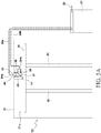
- FIG. 5A is a schematic drawing of an AM system 50 incorporating a bistatic THz inspection device comprising the bistatic THz probe 32 as shown in FIG. 3 .
- an AM system 50 comprises a material deposition chamber housing 51 (hereinafter "housing 51").
- a platform 59 onto which a build is manufactured is disposed within a material chamber 51a defined by housing 51.
- the platform 59 may be elevated within the housing 51 via a plurality of extendable legs 46 such that the part being manufactured is maintained within a predetermined distance from the material deposition head 11 at a "standoff' distance (d").
- the "standoff' distance (d") ranges from about 0.01" to about 0.1".
- Housing 51 is temperature controlled such that AM system 50 is configured to operate at elevated temperatures required for the additive manufacture of parts, including composite parts.
- the remainder of the features presented in the monostatic AM system 40 presented in FIGs. 4A and 4B are present in the bistatic AM system shown in FIGs. 5A and 5B , with the exception that a bistatic THz probe 32 replaces the monostatic THz probe 22 shown in FIGs. 4A and 4B .
- the bistatic THz probe 32 (also shown in FIG. 3 ) is positioned in situ proximate to the AM device 43.
- the THz probe 32 is spaced an "offset" distance (d') from the AM device 43 by spacers 44.
- the "offset" distance (d') ranges from about 0.5" to about 2.0".
- the spacers 44 need not be present in the AM system 50.
- the bistatic THz probe 32 shown in FIGs 5A and 5B comprises the features shown in FIG. 3 , including the thermal shield 36 encasing or otherwise substantially enveloping the THz probe 32.
- THz emitter 34a and THz receiver 34b are shown in communication respectively with fiber optic cables 38a and 38b.
- fiber optic cables 38a and 38b are in communication with controller 57.
- Power cable 58 is shown in communication with controller 57.
- Controller 57 can control and otherwise provide the THz wave source as well as house the data acquisition, signal processing, signal conditioning systems, etc. If desired, and although not shown in FIG. 5A , the controller 57 can further direct signals to or receive signals from a further controller or other device (e.g. a device used to supply signals, receive signals, and/or interpret a readout, etc.).
- a further controller or other device e.g. a device used to supply signals, receive signals, and/or interpret a readout, etc.
- aspects of the present disclosure find use in a variety of potential applications where composite parts are integrated into the overall manufacture of larger objects including, without limitation, vehicles, particularly vehicles in the aerospace, marine, automotive fields and other applications where lightweight and structurally robust parts are desired.
- objects and vehicles include, for example and without limitation, manned and unmanned aircraft, manned and unmanned spacecraft, manned and unmanned rotorcraft, manned and unmanned terrestrial vehicles, manned and unmanned surface water borne vehicles, manned and unmanned sub-surface water borne vehicles, satellites, etc.
- FIG. 6 is a representative illustration of an aircraft 60 comprising components, including structural components that are made according to the additive manufacturing and inspection processes disclosed herein.
- Aircraft 60 comprises fuselage section 62 and wing section 64.
- Vehicles including aircraft, as well as other structures, comprise many types of structural components that can be manufactured using the additive manufacturing and THz inspection apparatuses, systems and processes of the present disclosure, as well as larger objects that can incorporate such additively manufactured and concurrently inspected THz inspected structural components shown (e.g., AM structural components that are inspected via THz radiation substantially in real time during AM).
- Such exemplary components shown, as well as others not shown, can be made from additively manufactured materials, including, without limitation, composite materials.
- FIGs. 7 and 8 are flowcharts outlining methods according to aspects of the present disclosure.
- FIG. 7 illustrates a method 90 for additively manufacturing an additively manufactured part including additively manufacturing 92 a part by depositing a number of material layers from a printing head of an additive manufacturing device to form the part. At least one of the material layers is non-destructively inspected 94 by a method comprising directing 96 terahertz energy from the terahertz inspection device to a location on or within at least one material layer and receiving 97 terahertz energy from the at least one material layer component. Characteristics of the at least one material layer are then detected 98.
- FIG. 8 shows a method 100 for additively manufacturing an additively manufactured part including additively manufacturing 92 a part by depositing a number of material layers from a printing head of an additive manufacturing device to form the part.
- the material layers are deposited 102 at an elevated temperature depending upon the requirements of the material(s) being deposited and, for example, at a temperature ranging from about 300°F to about 450°F.
- Substantially concurrently with depositing the number of material layers at least one material layer is non-destructively inspected in real time relative to the material layer deposition, by substantially concurrently with depositing 104 at least one material layer non-destructively inspecting the at least one material layer in real time using THz radiation.
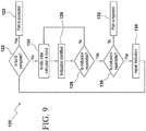
- FIGs. 9 and 10 are flowcharts outlining aspects of the present disclosure.
- a non-destructive inspection protocol 120 using THz radiation to inspect individual or a plurality of deposited AM layers as they are deposited in substantially real time is outlined in FIG. 9 .
- FIG. 9 shows that during an AM process for the AM manufacture of a secondary structure, a decision is made relative to inspecting a AM deposited build 122.
- the term "secondary structure" refers to structures including, for example, aircraft structures made from parts, including, without limitation, parts made from and comprising neat resins used to construct, e.g., airplane interior structures. Such secondary structure parts also include, for example, fittings, brackets, housings, etc., presently made from, or otherwise comprising metals.
- the part is accepted 123.
- in situ THz inspection of the build in substantially real time is conducted 124 and in situ data is collected.
- a potential anomaly e.g., an "indication”
- a decision is made regarding the indication and its impact on the build layer 128 and a decision is made regarding rejection of the build layer 128. If it is not necessary to reject such a build layer, the build is allowed to continue, with further data collected in real time during the AM build 124.
- the indication is determined to be rejectable 128, a decision is made regarding the nature of the indication relative to repair 130. If such a build layer or layers comprising the indication cannot be repaired, the part is rejected 132. If a repair can be made, the layer comprising the indication is repaired 134, and the build continues 122.
- a non-destructive inspection protocol 150 using THz radiation to inspect individual or a plurality of deposited AM layers as they are deposited in substantially real time for the AM manufacture of a primary structure is outlined in FIG. 10 .
- the term "primary structure" refers to structures including, for example, aircraft structures made from parts, including parts made from and comprising neat resins. Such parts are then used to construct large scale components including, for example, ribs, stringers, spars, longerons, etc. If a determination 130 is made that a discovered indication is not reparable, after a build is complete a post-process area of interest is further inspected 136 (e.g. as part of a quality control or other post-processing inspection.
- a post-processing inspection is performed of any rejectable indication of interest.
- An evaluation 140 is performed to determine and confirm whether or not an indication is rejectable. If the indication is confirmed as rejectable, the part is rejected 142. If the indication is not confirmed as rejectable, additional areas of the part may be conducted 144. If no further areas of interest to inspect are identified, the part is accepted 146. If additional areas of interest are identified for inspection, the part is re-evaluated according to boxes 138 through 144, as desired.
- Aircraft applications of the disclosed aspects may include, for example, and without limitation, additively manufacturing structural components such as, for example, spars, ribs, stringers, bulkheads, longerons, etc., and substantially concurrent with the additive manufacturing, non-destructively inspecting the AM structural component layers, individually in real time, or inspecting multiple layers, via applying THz energy to the component layers during the manufacturing process.
- additively manufacturing structural components such as, for example, spars, ribs, stringers, bulkheads, longerons, etc.
- aspects of the disclosure may be used in the context of an aircraft manufacturing and service method 200 and aircraft 300 including at least in the component and subassembly manufacturing 206, system integration 208, maintenance and service 214, in the assembly and maintenance of the aircraft airframe 302, and through aircraft interior 304.
- exemplary method 200 includes specification and design 202 of the aircraft 300 and material procurement 204.
- component and subassembly manufacturing 206 and system integration 208 of the aircraft 300 takes place.
- the aircraft 300 may go through certification and delivery 210 in order to be placed in service 212.
- routine maintenance and service 214 which may also include modification, reconfiguration, refurbishment, and so on.
- a system integrator may include, without limitation, any number of aircraft manufacturers and major-system subcontractors.
- a third party may include, without limitation, any number of vendors, subcontractors, and suppliers; and an operator may be an airline, leasing company, military entity, service organization, and so on.
- the aircraft 300 produced by exemplary method 200 can include an airframe 302 with a plurality of systems 303 and an interior 304.
- high-level systems 303 include, without limitation, one or more of a propulsion system 306, an electrical system 308, a hydraulic system 310, and an environmental system 312. Any number of other systems can be included.
- an aerospace example is shown, aspects of the present disclosure may be applied to other industries, such as the marine, automotive industries and/or other vehicular industries.
- Systems and methods set forth herein may be employed during any one or more of the stages of the production and service method 200.
- components or subassemblies corresponding to component and subassembly manufacture 206 may be fabricated or manufactured in a manner similar to components or subassemblies produced while the aircraft 300 is in service.
- one or more apparatuses, methods, or a combination thereof may be used during the production stages 206 and 208, for example, by substantially expediting assembly of or reducing the cost of an aircraft 300.
- one or more of apparatuses, systems, methods, or a combination thereof may be used while the aircraft 300 is in service such as, for example and without limitation, maintenance and service 214 of the aircraft 300.
- the disclosed apparatuses, systems and methods for additively manufacturing and concurrently inspecting in real time additively manufactured components find particular use in vehicles, including manned and unmanned aircraft, manned and unmanned spacecraft, manned and unmanned rotorcraft, manned and unmanned terrestrial vehicles, manned and unmanned surface water borne vehicles, manned and unmanned sub-surface water borne vehicles, satellites, etc.
- vehicles including manned and unmanned aircraft, manned and unmanned spacecraft, manned and unmanned rotorcraft, manned and unmanned terrestrial vehicles, manned and unmanned surface water borne vehicles, manned and unmanned sub-surface water borne vehicles, satellites, etc.
Landscapes
- Chemical & Material Sciences (AREA)
- Engineering & Computer Science (AREA)
- Materials Engineering (AREA)
- Manufacturing & Machinery (AREA)
- Physics & Mathematics (AREA)
- Health & Medical Sciences (AREA)
- General Health & Medical Sciences (AREA)
- Spectroscopy & Molecular Physics (AREA)
- Optics & Photonics (AREA)
- Analytical Chemistry (AREA)
- Toxicology (AREA)
- Mechanical Engineering (AREA)
- Biochemistry (AREA)
- General Physics & Mathematics (AREA)
- Immunology (AREA)
- Pathology (AREA)
- Life Sciences & Earth Sciences (AREA)
- Automation & Control Theory (AREA)
- Plasma & Fusion (AREA)
Abstract
Description
- The present disclosure relates generally to non-destructive testing methods. More specifically, the present disclosure relates to the use of Terahertz frequencies to non-destructively inspect manufactured parts.
- Additive manufacturing (equivalently referred to herein as "AM") is the broad term encompassing computer assisted 3-D printing techniques. The term "3-D printing" originally referred to a process that deposits a binder material onto a powder bed with inkjet printer heads layer-by-layer. More recently, the term is being used in popular vernacular to encompass a wider variety of additive manufacturing techniques. United States and global technical standards use the term "additive manufacturing" in this broader sense to connote manufacturing systems for producing three-dimensional (equivalently referred to herein as "3D") parts that are typically first fashioned digitally on a computer. For example, standard ISO/ASTM52900-15 defines seven categories of AM processes within its meaning: binder jetting, directed energy deposition, material extrusion, material jetting, powder bed fusion, sheet lamination and vat photopolymerization.
- The field of additive manufacturing has progressed to allow for layer-by-layer deposition of various materials. In many instances, additive manufacturing has proven useful in the manufacture of one-off parts including, for example, parts used as prototypes, or other customized parts that may or may not lead to mass production. However, the use of additive manufacturing techniques to make certain parts (e.g., load-bearing or structural parts) has not been accepted or even approved by certain standards, especially where inspections for quality and safety are required. The lack of accepted inspection techniques for additively manufactured parts, including additively manufactured parts used as load-bearing parts or other structural parts (e.g., additively manufactured parts requiring inspection and certification), has hampered the advancement of additively manufacturing structural parts.
- According to aspects of the present disclosure, apparatuses, systems and methods are presented for the non-destructive inspection of additively manufactured parts in real time during manufacture of the parts using radiation in the Terahertz frequency range.
- According to an aspect, the present disclosure is directed to an apparatus comprising an additive manufacturing device including a material deposition head configured to form an additively-manufactured build, with the build comprising individual layers of deposited material, and with the additive manufacturing device comprising a deposition head, and a terahertz inspection device located proximate to the material deposition head. The terahertz inspection device includes a terahertz probe, and further includes a thermal shield that substantially envelops the terahertz probe.
- According to another aspect, the present disclosure is directed to a system including a housing, an additive manufacturing device including a material deposition head located within the housing, with the material deposition head configured to deposit a plurality of successive material layers to form an additively manufactured part. The system further comprises a terahertz inspection device including a terahertz probe, with the probe located within the housing and with the probe located proximate to the material deposition head. The probe further includes a thermal shield substantially enveloping the probe.
- In another aspect, the terahertz inspection system is configured to non-destructively inspect at least one material layer in substantially real time during the deposit of the at least one material layer.
- According to a further aspect, the present disclosure is directed to a method for additively manufacturing a part, the method comprising individually depositing a plurality of material layers from a material deposition head of an additive manufacturing device to form a part. At least one of the individually deposited material layers are non-destructively inspected using terahertz energy. The method further comprises directing terahertz energy from a terahertz inspection device to a location on or within at least one material layer and receiving terahertz energy from at least one material layer and detecting characteristics of the at least one material layer being non-destructively inspected.
- In a further aspect, is directed to a method further comprising orienting the terahertz inspection device proximate to the material deposition head and depositing at least one material layer at a temperature ranging from about 300F to about 450F. Substantially concurrently with the depositing of the plurality of material layers, at least one material layer is non-destructively inspected in real time and the terahertz inspection device is substantially enveloped in a thermal shield.
- Another aspect of the present disclosure is directed to a structural component for a vehicle, including an aircraft, made and inspected according to methods disclosed herein, and an aircraft comprising structural components made and inspected according to methods disclosed herein.
- The features, functions and advantages that have been discussed can be achieved independently in various aspects or may be combined in yet other aspects, further details of which can be seen with reference to the following description and the drawings.
- Having thus described variations of the disclosure in general terms, reference will now be made to the accompanying drawings, which are not necessarily drawn to scale.
-
FIGs. 1A, 1B and 1C are perspective side views of an apparatus and system according to an aspect of the present disclosure. -
FIG. 2 is a perspective cross-sectional view of a THz probe used in connection with the apparatuses, systems and methods of the present disclosure featuring a monostatic THz probe orientation. -
FIG. 3 is a perspective cross-sectional view of a THz probe used in connection with the apparatuses, systems and methods of the present disclosure featuring a bistatic THz probe orientation. -
FIGs. 4A and4B are perspective cross-sectional side views of a system according to an aspect of the present disclosure featuring a monostatic THz probe orientation. -
FIG. 4B is an enlarged view of portions of the system shown inFIG. 4A . -
FIGs. 5A and5B are perspective cross-sectional side views of a system according to an aspect of the present disclosure featuring a bistatic THz probe orientation. -
FIG. 5B is an enlarged view of portions of the system shown inFIG. 4A . -
FIG. 6 is a representative illustration of an aircraft, said aircraft comprising structural components made according to aspects of the present disclosure. -
FIGs. 7 and8 are flowcharts outlining methods according to aspects of the present disclosure. -
FIGs. 9 and10 are flowcharts outlining further aspects of the present disclosure. -
FIG. 11 is a flow diagram of aircraft production and service methodology. -
FIG. 12 is a block diagram of an aircraft. - The present disclosure is directed to apparatuses, systems and methods for non-destructively inspecting additively manufactured parts in real time using terahertz (referred to equivalently herein as "THz") frequencies delivered from a THz probe positioned proximate to the additive manufacturing material deposition head, with the THz probe housed within a thermal shield encasing, or substantially enveloping, the THz probe.
- The THz frequency range refers to electromagnetic waves with frequencies between about 100 GHz and about 10 THz, or wavelengths between about 3 mm and about 30 µm existing in the radiation spectrum between the microwave and infrared regions. The present disclosure uses the terms "THz radiation", "THz energy", and "THz waves" equivalently. Terahertz waves pass through a variety of amorphous and opaque materials with high chemical selectivity, with the ability to image such material under THz interrogation with high definition. As is disclosed herein, non-destructive THz inspection techniques for interrogating dielectric (e.g., non-conducting) materials includes the inspection of composite materials.
- According to presently disclosed aspects, such AM processes or "3D manufacturing" processes progressively deposit extremely thin layers of material to create a 3D object from a computer assisted drawing (CAD) file or file formats that include Additive Manufacturing file (AMF) format. Additive manufacturing (AM) is presently understood as referring to processes used to create a three-dimensional (3D) object where layers of material are formed, typically under computer control, to create a manufactured object. Manufactured objects can be of almost any shape or geometry and are produced using digital model data from a 3D model or another electronic data source such as an AMF format. Therefore, compared to removing material from a stock piece, as may be done in a conventional machining process to form a part, 3D printing or AM builds a three-dimensional object from a computer-aided design (CAD) model or an AMF or STL file format by successively adding material layer-by-layer to accurately produce a part having a desired and/or predetermined dimension and/or geometry.
- As a result, aspects of the present invention contemplate the use of AM apparatuses, systems and processes to form an AM product (e.g., a part). A non-exhaustive list of such processes includes, without limitation, direct energy deposition; direct metal laser sintering; direct metal printing; electron beam additive manufacturing; electron beam melting; electron beam powder bed manufacturing; fused deposition modeling; fused filament fabrication; indirect powder bed manufacturing; laser cladding; laser deposition manufacturing; laser deposition welding; laser deposition welding/integrated milling; laser engineering net shaping; laser freeform manufacturing; laser metal deposition with powder; laser metal deposition with wire; laser powder bed manufacturing; laser puddle deposition; laser repair manufacturing; powder directed energy deposition; stereolithography; selective laser melting; selective laser sintering; small puddle deposition; or combinations thereof.
- Therefore, a large number of additive processes are available. The main differences between the listed processes are in the way that layers are deposited to create parts, and in the materials that are used. Some methods melt or soften the material to produce the layers. For example, in fused filament fabrication (FFF), also known as fused deposition modeling (FDM), the part is produced by extruding small beads or streams of material which harden immediately to form layers. Typically, a filament of thermoplastic material, or metal in the form of metal wire, or other material is fed into an extrusion nozzle head (e.g., a 3D printer extruder, or printer extruder head hereinafter equivalently referred to as a "printer head"), that heats the material and produces a deposit material flow. Another technique fuses parts of the layer and then moves "upward" in the working area, adding successive layers of material, and repeating the process until the piece has "built up" or formed a "build". This process uses the unfused media to support overhangs and thin walls in the part being produced, reducing the need for temporary auxiliary supports for the piece.
- In FFF processes, the printing head is moved, under computer control to define a desired build of desired 3D dimensions. Typically, the printer head deposits layers while moving in two dimensions to deposit one horizontal layer at a time before the printer head is directed to a position that is slightly "upward" (e.g., upward from the previously deposited layer) before depositing a subsequent layer onto the build. The speed of the deposition through the print head and the movement of the print head can be controlled to interrupt and re-start material deposition to form a defined interrupted region within a deposited layer.
- Laser sintering techniques include, without limitation, selective laser sintering with both metals and polymers, and direct metal laser sintering. Selective laser melting does not use sintering for the fusion of powder granules, but will completely melt the powder using a high-energy laser to create fully dense materials in a layer-wise deposition method that has mechanical properties similar to those of conventional manufactured metals. Electron beam melting is a similar type of additive manufacturing technology for metal parts (e.g. titanium, titanium alloys). EBM manufactures parts by melting metal powder layer by layer with an electron beam in a high vacuum. Another method consists of an inkjet 3D printing system that creates the part one layer at a time by spreading a layer of powder (plaster or resins) and printing a binder in the cross-section of the part using an inkjet-like process. With laminated object manufacturing, thin layers are cut to shape and joined together.
- Other methods cure liquid materials using different sophisticated technologies, such as sterolithography. Photopolymerization is primarily used in stereolithography to produce a solid part from a liquid. Inkjet printer systems like the Objet PolyJet system spray photopolymer materials onto a build tray in ultra-thin layers (e.g., between 16 µm and 30 µm) until the part is completed. Each photopolymer layer is cured with UV light after it is jetted, producing fully cured models that can be handled and used without post-curing. Further, ultrasmall features can be made with the 3D micro-fabrication technique used in multiphoton photopolymerization. Due to the nonlinear nature of photo excitation, a gel is cured to a solid only in the places where the laser was focused while the remaining gel is removed. Feature sizes of less than about 100 nm can be produced, as well as complex structures that can comprise moving and interlocked parts.
- Yet another approach uses a synthetic resin that is solidified using LEDs. In Mask-image-projection-based stereolithography, a 3D digital model is sliced by a set of horizontal planes. Each slice is converted into a two-dimensional mask image. The mask image is then projected onto a photocurable liquid resin surface and light is projected onto the resin to cure it in the shape of the layer. Continuous liquid interface production begins with a reservoir of liquid photopolymer resin. Part of the reservoir is transparent to ultraviolet light, causing the resin to solidify.
- In powder-fed directed-energy deposition, a high-power laser is used to melt metal powder supplied to the focus of the laser beam. The powder fed directed energy process is similar to Selective Laser Sintering, but the metal powder is applied only where material is being added to the part at that moment.
- Aspects of the present disclosure contemplate the use of FFF and FDM processes, although any of the aforementioned deposition techniques and processes are contemplated. Exemplary FFF and FDM apparatuses used in the contemplated AM processes to manufacture the desire builds include systems capable of depositing material at temperatures up to about 428F, depending on the desired mechanical properties of the build. According to further contemplated aspects, deposition rates of the deposited layers is controlled to effect a deposition rate ranging from about 4 to about 6 inches/sec.
- According to present aspects, a wide variety of materials can be extruded from the printer head of the FFF and FDM apparatuses, including, without limitation, thermoplastics, such as acrylonitrile butadiene styrene (ABS), polyacetic acid, high-impact polystyrene, thermoplastic polyurethane, aliphatic polyamides, polyether ether ketones (PEEKs), as well as composite materials, including ceramics.
- According to aspects of the present disclosure, the additive manufacturing and substantially simultaneous THz inspection of deposited layers of composite and other materials including, without limitation, layers deposited via additive manufacturing processes comprising carbon fiber resin materials. Such carbon fiber resin materials supplied to an additive manufacturing device and system include materials supplied as feedstock, for example, in the form of neat resin further comprising fiber particulate material. Further, representative resin materials for use to incorporate carbon fibers and fiber glass-incorporated material systems, according to aspects of the present disclosure include, without limitation and for example, ULTEM 9085, polyetherketoneketone (PEKK), polycarbonate-ABS, polycarbonate, Vero, digital-ABS Plus, FDM Nylon 6;
FDM nylon 12 CF;DFM Nylon 12; ULTEM 1010 (Stratasys, Ltd.); PPSF Model (Stratasys, Ltd.) etc. - According to aspects of the present disclosure, THz radiation is emitted from the customized THz inspection device, referred to equivalently herein as a "THz probe", or a THz inspection head". The THz probe is used in conjunction with an additive manufacturing system to non-destructively evaluate AM parts, by inspecting an individual deposited layer or layers in situ, and substantially in real time. Accordingly, the apparatuses, systems and methods of the present disclosure identify abnormalities in the AM parts as the parts are being fabricated, (e.g., during material deposition of each or selected layers, and therefore before completion of the entire part). That is, the THz inspection device is configured to inspect at least one individual layer of deposited material in substantially real time during material deposition. For purposes of the present disclosure the term "substantially in real time" connote a time duration that approximates the time required to deposit a layer from an AM device print head to a build. The precise quantifiable amount of time required to deposit such a layer is dependent on the dimensions of the part being built, as well as many other deposition and manufacturing parameters. However, the aspects of the present disclosure contemplate an inspection, via THz radiation, of an individual layer (or desired number of layers of an AM build) occurring substantially concurrently with the depositing of the individual layer or layers of a build.
- In a further aspect, the apparatuses and systems disclosed herein comprise a thermal shield configured to house and substantially envelop the THz probe. The THz probe is oriented proximate to the additive manufacturing material deposition device and head within an additive manufacturing chamber or housing. The additive manufacturing chamber operates at an elevated temperature as successive material layers are deposited.
- In a further aspect, in the process of additively manufacturing a part by depositing a number of material layers, the material layers are deposited at a temperature ranging from about 300°F to about 450°F. and more particularly ranging from about 300°F to about 428°F. Substantially concurrently with the step of depositing the number of material layers, non-destructive THz inspection of at least one of the material layers is conducted substantially in situ and substantially in real time.
- Sensitive inspection instrumentation, including the use of THz probes, can be adversely impacted by significantly elevated temperature environments. This has limited the technology available to non-destructively inspect parts, requiring a delay of the inspection until part manufacturing has been completed. According to aspects of the present disclosure, at least one non-destructive inspection device in the form of at least one THz probe is oriented in situ proximate to the deposition head of an additive manufacturing device while the device operates in an elevated temperature environment (e.g., ranging from about 300°F to about 450°F), with the THz probe encased or substantially enveloped in a protective thermal shield.
- According to aspects of the present disclosure, the real time inspection of incremental deposited layers of additively manufactured parts using a THz inspection device positioned proximate to the material deposition head facilitates the inspection of an additively manufactured part during a build. The apparatuses, systems, and methods of the present disclosure enable the substantially real time detection of anomalies in an AM layer or layers during the build. In this way, such anomalies can be addressed much sooner in the manufacturing process.
- Early detection of such anomalies reduces material waste, obviates part replacement and commensurate cost and potentially increases safety. Further, such early detection can impart required part inspection and quality for AM parts that may enable the certification of AM structural parts used in many industries, including the aircraft and aerospace industries.
-
FIGs. 1A, 1B, and 1C are schematic representations of stages of an AM process according to aspects of the present disclosure that are utilized to form apart 16. As shown inFIG. 1A , afirst stage 10a of an additive manufacturing material deposition process includes amaterial deposition head 11 oriented proximate to aTHz probe 12, with thematerial deposition head 11 shown depositing abuild 13. Thebuild 13 comprises successively depositedindividual material layers 13a. As shown inFIG. 10a , a (fourth) partially depositedmaterial layer 14a is being deposited and incorporated into thebuild 13.FIG. 1B shows asecond stage 10b of the process, where the (fourth) partially depositedmaterial layer 14a has now been fully deposited to become a completed depositedmaterial layer 14b included in thebuild 13.FIG. 1C shows athird stage 10c of the process where asubsequent material layer 15 is being deposited ontomaterial layer 14b, and is adding a layer to thebuild 13. In operation, material layers are continually added to thebuild 13 until thepart 16 is completed. As shown inFIGs. 1A, 1B, and 1C , thematerial deposition head 11 is oriented proximate to, and at a predetermined distance from the THz probe. According to an aspect of the present disclosure, the deposition head is oriented at a distance from the THz probe ranging from about 0.5" to about 2.0". -
FIG. 2 is a cross-sectional view of amonostatic THz probe 22 showing theTHz probe 22 substantially enveloped or encased within athermal shield 26.Monostatic THZ probe 22 is shown in communication with afiber optic cable 28, although any suitable connection for a THz probe is presently contemplated.Monostatic THz probe 22 further comprises a THz emitter/receiver 24 in communication withfiber optic cable 28. During operation, the THz radiation proceeds from the THz emitter/receiver 24 in the direction oflens 27, and proceeds from themonostatic THz probe 22 to a targeted region of a substrate toward which themonostatic THz probe 22 is directed. In the emitting mode, the emitter/receiver 24 and thelens 27 are constructed or otherwise selected to set a focus and to refract radiation to a predetermined distance from the emitter/receiver 24. In the receiving mode, data is captured by the emitter/receiver 24 as raw waveforms of the THz reflections from the target (not shown inFIG. 2 ). The inspected target can be a build layer surface or build layer subsurface. According to present aspects, individual build layers can be deposited at average thicknesses ranging from about 0.005" to about 0.020" thick. - As shown in
FIG. 2 , the outer surface ofmonostatic THz probe 22 is encased or otherwise substantially enveloped bythermal shield 26. In the monostatic inspection mode, themonostatic THz probe 22 accomplishes both the transmission and receiving functions in a single unit. Thethermal shield 26 will not interfere with the monostatic THz probe's ability to emit THz radiation from the probe. The terms "encased", "substantially encased" and "substantially enveloped" refer to a state where thethermal shield 26 encases or surrounds a predominant portion of themonostatic THz probe 22 to an extent where the probe is able to operate in an elevated temperature environment ranging from about 300°F to about 450°F, and therefore may not completely envelop themonostatic THz probe 22. -
FIG. 3 is a cross-sectional view of abistatic THz probe 32 showing thebistatic THz probe 32 substantially enveloped or encased within athermal shield 36. In the bistatic arrangement, theTHZ probe 32 include aTHz emitter 34a and aTHz receiver 34b in communication withfiber optic cable - During operation, the THz radiation proceeds from and is emitted by the
THz emitter 34a toward and throughoptical element 35 to the surface or subsurface of the build layer or layers.Optical element 35 as shown can be a one-way mirror such that wavelengths reflected back to probe 22 are directed byoptical element 35 to thereceiver 34b. As shown, the outer surface ofbistatic THz probe 32 is encased or otherwise substantially enveloped bythermal shield 36. In the bistatic inspection mode, theTHz probe emitter 34a emits THz radiation directed through theoptical element 35 to a target to be inspected (not shown). THz radiation then returns from the target (not shown) into THz probe, where the THz radiation is reflected fromoptical element 35 toTHz receiver 34b. It is recognized that thethermal shield 36 will not interfere with the bistatic THz probe's ability to emit THz radiation from theTHz probe emitter 34a and receive THz radiation from a target by theTHz receiver 34b. The terms "encased", "substantially encased" and "substantially enveloped" refer to a state where thethermal shield 36 encases or surrounds a predominant portion of thebistatic THz probe 32 to an extent where the probe is able to operate in an environment having an elevated temperature environment ranging from about 300°F to about 450°F, and therefore may not completely envelop thebistatic THz probe 32. - As shown in the bistatic arrangement shown in
FIG. 3 , theTHz emitter 34a and thelens 37 are constructed or otherwise selected to set a focus and to refract radiation to a predetermined distance from the emitter/receiver 34a. TheTHz receiver 34b captures data as raw waveforms of the THz reflections from the target (not shown inFIG. 3 ). - With respect to both the monostatic and bistatic configurations, the inspected target can be a build layer surface or build layer subsurface. According to present aspects, individual build layers can be deposited at average thicknesses ranging from about 0.005" to about 0.020" thick. The raw waveforms are received from the inspected target and processed through filters and data acquisition and interpretation software to evidence differences (e.g., anomalies) between expected and varying results over a targeted surface area. According to aspects of the present disclosure, the software converts the waveforms into an output in the form of, for example, C-scans, B-scans, etc., of targets corresponding to individual build layers in substantially in real time (e.g., viewed or otherwise interpreted on an output "live") relative to the depositing of such individual layers onto the build.
- The
thermal shield 26, 36 (as shown inFIGs. 2, 3 ,4A ,4B ,5A and5B ) that encases, or substantially envelops theTHz probe - The
thermal shield - Any material deposition method for depositing the thermal shield onto the outer surface of a THz probe is presently contemplated. Further, the casing or housing of the thermal probe itself may be made from a thermally shielding material. In this aspect, the thermal shield material acts both as a structural part of the THz probe while also acting as a thermal shield, so long as the thermal shield material is robust enough to structurally support and house the components contained in the THz probe.
-
FIG. 4A is a schematic drawing of anAM system 40 incorporating a monostatic THz inspection device having themonostatic THz probe 22 as shown inFIG. 2 .FIG. 4B is an enlarged view of a portion of the system shown inFIG. 4A . As shown inFIG. 4A , anAM system 40 comprises a material deposition chamber housing 41 (hereinafter "housing 41"). Aplatform 49 onto which a build is manufactured is disposed within amaterial deposition chamber 41a defined by thehousing 41. As shown inFIG. 4A , theplatform 49 may be elevated within thehousing 41 via a plurality ofextendable legs 46. As shown inFIGs 4A and4B , the part being manufactured is maintained within a predetermined distance from thematerial deposition head 11 at a "standoff' distance (d"). According to aspects of the present disclosure, the "standoff distance (d") ranges from about 0.01" to about 0.1".Housing 41 is temperature controlled such thatAM system 40 is configured to operate at elevated temperatures required for the additive manufacture of parts, including composite parts; such operating temperatures ranging from about 300°F to about 450°F or more.Additive manufacturing device 43 withmaterial deposition head 11 is positioned proximate to buildplatform 49. - The
monostatic THz probe 22 is positioned proximate to theAM device 43. As shown inFIGs. 4A and4B , themonostatic THz probe 22 is spaced an "offset" distance (d') from theAM device 43 byspacers 44. According to aspects of the present disclosure, the "offset" distance (d') ranges from about 0.5" to about 2.0". Alternatively, thespacers 44 need not be present in thesystem 40. InFIGs. 4A and4B , themonostatic THz probe 22 comprises the features described herein and shown inFIG. 2 , includingthermal shield 26 encasing or otherwise substantially enveloping themonostatic THz probe 22, and the THz emitter/receiver 24 in communication withfiber optic cable 28, andlens 27. - As shown in
FIG. 4A ,fiber optic cable 28 is in communication withcontroller 47.Power cable 48 is shown in communication withcontroller 47. Thepower cable 48 engages a power source (not shown).Controller 47 can control and otherwise provide the THz wave source as well as house the data acquisition, signal processing, signal conditioning systems, etc., described herein. If desired, and although not shown inFIG. 4A , thecontroller 47 can further direct signals to or receive or send signals from a further controller or other device (e.g., a device used to supply signals, receive signals and/or interpret a readout, etc.). -
FIG. 5A is a schematic drawing of anAM system 50 incorporating a bistatic THz inspection device comprising thebistatic THz probe 32 as shown inFIG. 3 . As shown inFIG. 5 , anAM system 50 comprises a material deposition chamber housing 51 (hereinafter "housing 51"). Aplatform 59 onto which a build is manufactured is disposed within amaterial chamber 51a defined byhousing 51. As shown inFIG 5A , theplatform 59 may be elevated within thehousing 51 via a plurality ofextendable legs 46 such that the part being manufactured is maintained within a predetermined distance from thematerial deposition head 11 at a "standoff' distance (d"). According to aspects of the present disclosure, the "standoff' distance (d") ranges from about 0.01" to about 0.1".Housing 51 is temperature controlled such thatAM system 50 is configured to operate at elevated temperatures required for the additive manufacture of parts, including composite parts. The remainder of the features presented in themonostatic AM system 40 presented inFIGs. 4A and4B are present in the bistatic AM system shown inFIGs. 5A and5B , with the exception that abistatic THz probe 32 replaces themonostatic THz probe 22 shown inFIGs. 4A and4B . As shown inFIGs. 5A and5B , the bistatic THz probe 32 (also shown inFIG. 3 ) is positioned in situ proximate to theAM device 43. As further shown inFIGs. 5A and5B , theTHz probe 32 is spaced an "offset" distance (d') from theAM device 43 byspacers 44. According to aspects of the present disclosure, the "offset" distance (d') ranges from about 0.5" to about 2.0". Alternatively, thespacers 44 need not be present in theAM system 50. Thebistatic THz probe 32 shown inFIGs 5A and5B comprises the features shown inFIG. 3 , including thethermal shield 36 encasing or otherwise substantially enveloping theTHz probe 32.THz emitter 34a andTHz receiver 34b are shown in communication respectively withfiber optic cables - As shown in
FIG. 5A ,fiber optic cables controller 57.Power cable 58 is shown in communication withcontroller 57.Controller 57 can control and otherwise provide the THz wave source as well as house the data acquisition, signal processing, signal conditioning systems, etc. If desired, and although not shown inFIG. 5A , thecontroller 57 can further direct signals to or receive signals from a further controller or other device (e.g. a device used to supply signals, receive signals, and/or interpret a readout, etc.). - Aspects of the present disclosure find use in a variety of potential applications where composite parts are integrated into the overall manufacture of larger objects including, without limitation, vehicles, particularly vehicles in the aerospace, marine, automotive fields and other applications where lightweight and structurally robust parts are desired. Such objects and vehicles include, for example and without limitation, manned and unmanned aircraft, manned and unmanned spacecraft, manned and unmanned rotorcraft, manned and unmanned terrestrial vehicles, manned and unmanned surface water borne vehicles, manned and unmanned sub-surface water borne vehicles, satellites, etc.
-
FIG. 6 is a representative illustration of anaircraft 60 comprising components, including structural components that are made according to the additive manufacturing and inspection processes disclosed herein.Aircraft 60 comprisesfuselage section 62 andwing section 64. - Vehicles, including aircraft, as well as other structures, comprise many types of structural components that can be manufactured using the additive manufacturing and THz inspection apparatuses, systems and processes of the present disclosure, as well as larger objects that can incorporate such additively manufactured and concurrently inspected THz inspected structural components shown (e.g., AM structural components that are inspected via THz radiation substantially in real time during AM). Such exemplary components shown, as well as others not shown, can be made from additively manufactured materials, including, without limitation, composite materials.
-
FIGs. 7 and8 are flowcharts outlining methods according to aspects of the present disclosure.FIG. 7 illustrates amethod 90 for additively manufacturing an additively manufactured part including additively manufacturing 92 a part by depositing a number of material layers from a printing head of an additive manufacturing device to form the part. At least one of the material layers is non-destructively inspected 94 by a method comprising directing 96 terahertz energy from the terahertz inspection device to a location on or within at least one material layer and receiving 97 terahertz energy from the at least one material layer component. Characteristics of the at least one material layer are then detected 98. -
FIG. 8 shows amethod 100 for additively manufacturing an additively manufactured part including additively manufacturing 92 a part by depositing a number of material layers from a printing head of an additive manufacturing device to form the part. The material layers are deposited 102 at an elevated temperature depending upon the requirements of the material(s) being deposited and, for example, at a temperature ranging from about 300°F to about 450°F. Substantially concurrently with depositing the number of material layers, at least one material layer is non-destructively inspected in real time relative to the material layer deposition, by substantially concurrently with depositing 104 at least one material layer non-destructively inspecting the at least one material layer in real time using THz radiation. -
FIGs. 9 and10 are flowcharts outlining aspects of the present disclosure. Anon-destructive inspection protocol 120 using THz radiation to inspect individual or a plurality of deposited AM layers as they are deposited in substantially real time is outlined inFIG. 9 . As shown inFIG. 9 , during an AM process for the AM manufacture of a secondary structure, a decision is made relative to inspecting a AM depositedbuild 122. The term "secondary structure" refers to structures including, for example, aircraft structures made from parts, including, without limitation, parts made from and comprising neat resins used to construct, e.g., airplane interior structures. Such secondary structure parts also include, for example, fittings, brackets, housings, etc., presently made from, or otherwise comprising metals. If the build is complete and the part passes THz inspection in substantially real time, the part is accepted 123. Before determining acceptance of the part, in situ THz inspection of the build in substantially real time is conducted 124 and in situ data is collected. Upon detecting a potential anomaly (e.g., an "indication") 126 in a THz inspected build layer or in a plurality of THz inspected build layers, a decision is made regarding the indication and its impact on thebuild layer 128 and a decision is made regarding rejection of thebuild layer 128. If it is not necessary to reject such a build layer, the build is allowed to continue, with further data collected in real time during theAM build 124. If the indication is determined to be rejectable 128, a decision is made regarding the nature of the indication relative to repair 130. If such a build layer or layers comprising the indication cannot be repaired, the part is rejected 132. If a repair can be made, the layer comprising the indication is repaired 134, and the build continues 122. - A
non-destructive inspection protocol 150 using THz radiation to inspect individual or a plurality of deposited AM layers as they are deposited in substantially real time for the AM manufacture of a primary structure is outlined inFIG. 10 . The term "primary structure" refers to structures including, for example, aircraft structures made from parts, including parts made from and comprising neat resins. Such parts are then used to construct large scale components including, for example, ribs, stringers, spars, longerons, etc. If adetermination 130 is made that a discovered indication is not reparable, after a build is complete a post-process area of interest is further inspected 136 (e.g. as part of a quality control or other post-processing inspection. In addition, once a build is completed 122, a post-processing inspection is performed of any rejectable indication of interest. Anevaluation 140 is performed to determine and confirm whether or not an indication is rejectable. If the indication is confirmed as rejectable, the part is rejected 142. If the indication is not confirmed as rejectable, additional areas of the part may be conducted 144. If no further areas of interest to inspect are identified, the part is accepted 146. If additional areas of interest are identified for inspection, the part is re-evaluated according toboxes 138 through 144, as desired. - Aircraft applications of the disclosed aspects may include, for example, and without limitation, additively manufacturing structural components such as, for example, spars, ribs, stringers, bulkheads, longerons, etc., and substantially concurrent with the additive manufacturing, non-destructively inspecting the AM structural component layers, individually in real time, or inspecting multiple layers, via applying THz energy to the component layers during the manufacturing process.
- Referring now to
FIGs. 11 and 12 , aspects of the disclosure may be used in the context of an aircraft manufacturing andservice method 200 andaircraft 300 including at least in the component andsubassembly manufacturing 206,system integration 208, maintenance andservice 214, in the assembly and maintenance of theaircraft airframe 302, and throughaircraft interior 304. - During pre-production, as shown in
FIGs. 11 and 12 ,exemplary method 200 includes specification anddesign 202 of theaircraft 300 andmaterial procurement 204. During production, component andsubassembly manufacturing 206 andsystem integration 208 of theaircraft 300 takes place. Thereafter, theaircraft 300 may go through certification anddelivery 210 in order to be placed inservice 212. While in service by a customer, theaircraft 200 is scheduled for routine maintenance andservice 214, which may also include modification, reconfiguration, refurbishment, and so on. - Each of the processes of
method 200 can be performed or carried out by a system integrator, a third party, and/or an operator (e.g., a customer). For the purposes of this description, a system integrator may include, without limitation, any number of aircraft manufacturers and major-system subcontractors. Further, a third party may include, without limitation, any number of vendors, subcontractors, and suppliers; and an operator may be an airline, leasing company, military entity, service organization, and so on. - As shown in
FIG. 12 , theaircraft 300 produced byexemplary method 200 can include anairframe 302 with a plurality ofsystems 303 and an interior 304. Examples of high-level systems 303 include, without limitation, one or more of apropulsion system 306, anelectrical system 308, ahydraulic system 310, and anenvironmental system 312. Any number of other systems can be included. Although an aerospace example is shown, aspects of the present disclosure may be applied to other industries, such as the marine, automotive industries and/or other vehicular industries. - Systems and methods set forth herein may be employed during any one or more of the stages of the production and
service method 200. For example, components or subassemblies corresponding to component andsubassembly manufacture 206 may be fabricated or manufactured in a manner similar to components or subassemblies produced while theaircraft 300 is in service. Also, one or more apparatuses, methods, or a combination thereof may be used during the production stages 206 and 208, for example, by substantially expediting assembly of or reducing the cost of anaircraft 300. Similarly, one or more of apparatuses, systems, methods, or a combination thereof may be used while theaircraft 300 is in service such as, for example and without limitation, maintenance andservice 214 of theaircraft 300. - The disclosed apparatuses, systems and methods for additively manufacturing and concurrently inspecting in real time additively manufactured components, including structural components from various materials (e.g. composite material, etc.) find particular use in vehicles, including manned and unmanned aircraft, manned and unmanned spacecraft, manned and unmanned rotorcraft, manned and unmanned terrestrial vehicles, manned and unmanned surface water borne vehicles, manned and unmanned sub-surface water borne vehicles, satellites, etc.
- Further, the disclosure comprises embodiments according to the following numbered clauses:
- Clause 1 An apparatus comprising:
- an additive manufacturing device comprising a material deposition head; and
- a terahertz inspection device located proximate to the material deposition head; said terahertz inspection device comprising a terahertz probe, said terahertz probe comprising a thermal shield substantially enveloping the terahertz probe.
- Clause 2 The apparatus of Clause 1, wherein the additive manufacturing device is configured to form an additively manufactured build, said build comprising a plurality of individually deposited layers of material.
- Clause 3 The apparatus of Clause 1 or 2, wherein the terahertz inspection device is configured to non-destructively inspect individual deposited layers of material.
- Clause 4 The apparatus of any preceding Clause, wherein the terahertz inspection device is configured to inspect individual deposited layers of material substantially in real time during the depositing of the material layers.
- Clause 5 The apparatus of any preceding Clause, further comprising a material deposition chamber, said chamber defined by a housing, and said material deposition chamber configured to house said material deposition device and said terahertz inspection device.
- Clause 6 The apparatus of any preceding Clause, wherein the material deposition head is oriented within a first distance from the terahertz inspection device, said first distance ranging from about 0.5" to about 2.0".
- Clause 7 The apparatus of any preceding Clause, wherein the terahertz inspection device comprises a monostatic terahertz probe.
- Clause 8 The apparatus of any preceding Clause, wherein the terahertz inspection device comprises a bistatic terahertz probe.
- Clause 9 The apparatus of any preceding Clause, wherein the terahertz inspection device comprises a lens said lens selected to focus terahertz radiation at a predetermined distance from the terahertz inspection device.
- Clause 10 The apparatus of any preceding Clause, wherein the thermal shield is made from a material comprising at least one of; a ceramic; sodium silicate; potassium silicate; calcium silicate; tantalum carbide; hafnium carbide; a high temperature bismaleimide resin-containing material; a high temperature polyimide containing material; or a fiberglass-containing material.
-
Clause 11 The apparatus of any preceding Clause, wherein the thermal shield is made from a material comprising ceramic material. - Clause 12 A system comprising:
- a housing;
- an additive manufacturing device comprising a material deposition head, said material deposition head located within the housing, said
- material deposition head configured to deposit a plurality of material layers to form a part; and
- a terahertz inspection device located within the housing and further located proximate to the additive manufacturing device, said terahertz inspection device comprising a thermal shield substantially enveloping the terahertz inspection device.
-
Clause 13 The system ofClause 12, wherein, the terahertz inspection device is configured to non-destructively inspect in substantially real time at least one deposited material layer during or immediately after the deposit of the at least one deposited material layer. - Clause 14 The system of
Clause -
Clause 15 The system of any ofClauses 12 to 14, wherein the additive manufacturing device is in communication with a supply of feedstock material. -
Clause 16 The system ofClause 15, wherein the feedstock material comprises at least one of ULTEM 9085; FDM Nylon 6, FDM Nylon 12CF,DFM Nylon 12, ULTEM 1010; a polyetherketoneketone or a polyphenylsulfone. - Clause 17 A method for additively manufacturing an additively manufactured part, the method comprising:
- individually depositing a plurality of material layers from a material deposition head of an additive manufacturing device to form the part, and
- non-destructively inspecting at least one material layer using terahertz energy, and further comprising:
- directing terahertz energy from a terahertz inspection device to a location on or within the at least one material layer;
- receiving terahertz energy from the at least one material layer; and
- detecting characteristics of the at least one material layer.
- Clause 18 The method of Clause 17, further comprising:
- orienting the terahertz inspection device proximate to the material deposition head;
- depositing at least one material layer at a temperature ranging from about 300°F to about 450°F;
- substantially concurrently with the depositing of the plurality of material layers, nondestructively inspecting at least one material layer in real time; and
- wherein, said terahertz inspection device is substantially enveloped in a thermal shield.
- Clause 19 The method of Clause 17 or 18, further comprising:
detecting characteristics of the at least one material layer in real time during or immediately after depositing at least one material layer onto a build. - Clause 20 An additively manufactured part manufactured and inspected according to the method of any of Clauses 17 to 19.
- Aspects of the present disclosure can, of course, be carried out in other ways than those specifically set forth herein without departing from essential characteristics of aspects disclosed herein. The presently disclosed aspects are to be considered in all respects as illustrative and not restrictive, and all changes coming within the meaning and equivalency range of the appended claims are intended to be embraced therein.
Claims (15)
- An additive manufacturing system (40, 50) comprising:an additive manufacturing device (43) comprising a material deposition head (11); anda terahertz inspection device (12) located proximate to the material deposition head (11);said terahertz inspection device (12) comprising a terahertz probe (22, 32), saidterahertz probe (22, 32) comprising a thermal shield (26, 36) substantially enveloping the terahertz probe (22, 32).
- The additive manufacturing system (40, 50) of Claim 1, wherein the additive manufacturing device (43) is configured to form an additively manufactured build (13), said build (13) comprising a plurality of individually deposited layers of material (13a, 14, 15).
- The additive manufacturing system (40, 50) of any of Claims 1 to 2, wherein the terahertz inspection device (12) is configured to non-destructively inspect individual deposited layers of material (13a, 14, 15).
- The additive manufacturing system (40, 50) of any of Claims 1 to 3, wherein the terahertz inspection device (12) is configured to inspect individual deposited layers of material substantially in real time during the depositing of the material layers.
- The additive manufacturing system (40, 50) of any of Claims 1 to 4, further comprising a material deposition chamber (41a, 51a), said chamber (41a, 51a) defined by a housing (41, 51), and said material deposition chamber (41a, 51a) configured to house said material deposition head (11) and said terahertz inspection device (12).
- The additive manufacturing system (40, 50) of any of Claims 1 to 5, wherein the material deposition head (11) is oriented within a first distance from the terahertz inspection device (12), said first distance ranging from about 0.5" to about 2.0".
- The additive manufacturing system (40, 50) of any of Claims 1 to 6, wherein the terahertz inspection device (12) comprises a monostatic terahertz probe (22, 32).
- The additive manufacturing system (40, 50) of any of Claims 1 to 7, wherein the terahertz inspection device (12) comprises a bistatic terahertz probe (22, 32).
- The additive manufacturing system (40, 50) of any of Claims 1 to 8, wherein the terahertz inspection device (12) comprises a lens(27, 37), said lens (27, 37) selected to focus terahertz radiation to a predetermined distance from the terahertz inspection device (12).
- The additive manufacturing system (40, 50) of any of Claims 1 to 9, wherein the thermal shield (26, 36) is made from a material comprising at least one of; a ceramic; sodium silicate; potassium silicate; calcium silicate; tantalum carbide; hafnium carbide; a high temperature bismaleimide resin-containing material; a high temperature polyimide containing material; or a fiberglass-containing material.
- The additive manufacturing system (40, 50) of any of Claims 1 to 10, wherein the thermal shield (26, 36) is made from a material comprising a ceramic material.
- A method (90, 100) for additively manufacturing an additively manufactured part, the method comprising:individually depositing (92) a plurality of material layers from a material
deposition head (11) of an additive manufacturing device (43) to form the part, andnon-destructively inspecting (94) at least one material layer using terahertz energy, and further comprising:directing terahertz energy (96) from a terahertz inspection device (12) to a location on or within the at least one material layer;receiving terahertz energy (97) from the at least one material layer; anddetecting characteristics (98) of the at least one material layer. - The method of Claim 12, further comprising:orienting the terahertz inspection device (12) proximate to the material deposition head (11);depositing (102) at least one material layer at a temperature ranging from about 300°F to about 450°F;substantially concurrently with the depositing of the plurality of material layers, nondestructively inspecting at least one material layer in real time; andwherein, said terahertz inspection device (12) is substantially enveloped in a thermal shield.
- The method of any of Claims 12 to 13, further comprising:
detecting characteristics (98) of the at least one material layer in real time during or immediately after depositing at least one material layer onto a build (13). - An additively manufactured part manufactured and inspected according to the method of any of Claims 12 to 14.
Applications Claiming Priority (1)
| Application Number | Priority Date | Filing Date | Title |
|---|---|---|---|
| US15/887,518 US10773458B2 (en) | 2018-02-02 | 2018-02-02 | Terahertz inspection for additively manufactured materials |
Publications (2)
| Publication Number | Publication Date |
|---|---|
| EP3520931A1 true EP3520931A1 (en) | 2019-08-07 |
| EP3520931B1 EP3520931B1 (en) | 2023-05-10 |
Family
ID=65279410
Family Applications (1)
| Application Number | Title | Priority Date | Filing Date |
|---|---|---|---|
| EP19154612.6A Active EP3520931B1 (en) | 2018-02-02 | 2019-01-30 | Terahertz inspection for additively manufactured materials |
Country Status (4)
| Country | Link |
|---|---|
| US (1) | US10773458B2 (en) |
| EP (1) | EP3520931B1 (en) |
| CN (1) | CN110132883B (en) |
| IL (1) | IL264563B2 (en) |
Families Citing this family (3)
| Publication number | Priority date | Publication date | Assignee | Title |
|---|---|---|---|---|
| US10871471B1 (en) * | 2020-01-02 | 2020-12-22 | The Boeing Company | Systems and methods for inspecting additively manufactured components |
| DE102020121471A1 (en) | 2020-08-14 | 2022-02-17 | Fraunhofer-Gesellschaft zur Förderung der angewandten Forschung eingetragener Verein | METHODS AND SYSTEMS FOR ADDITIVE MANUFACTURING AND CHARACTERIZATION OF AN OBJECT |
| US12196543B2 (en) | 2022-04-06 | 2025-01-14 | The Boeing Company | System for in-process inspection of fused-filament fabricated parts and associated methods |
Citations (3)
| Publication number | Priority date | Publication date | Assignee | Title |
|---|---|---|---|---|
| US9108358B1 (en) * | 2014-04-10 | 2015-08-18 | Xerox Corporation | System for real time monitoring for defects in an object during three-dimensional printing using a terahertz sensor |
| WO2016128757A1 (en) * | 2015-02-13 | 2016-08-18 | Zircotec Ip Limited | A heat shield and a heat shield assembly |
| US20170217101A1 (en) * | 2016-01-29 | 2017-08-03 | Samsung Electronics Co., Ltd. | Sensing device capable of detecting hardness, mobile device having the same, and three-dimensional printing apparatus using the same |
Family Cites Families (7)
| Publication number | Priority date | Publication date | Assignee | Title |
|---|---|---|---|---|
| KR102143540B1 (en) * | 2012-10-19 | 2020-08-11 | 피코메트릭스 엘엘씨 | Calculating material properties using reflection terahertz radiation |
| US9244004B2 (en) * | 2013-08-08 | 2016-01-26 | Stichting Sron—Netherlands Institute For Space Research | Method and system for inspection of composite assemblies using terahertz radiation |
| CN103983293B (en) * | 2014-05-15 | 2016-09-07 | 中国电子科技集团公司第四十一研究所 | A kind of THz photodetector absolute spectral response rate calibrating installation and method |
| US10580611B2 (en) * | 2014-08-21 | 2020-03-03 | Raytheon Company | Rapid 3D prototyping and fabricating of slow-wave structures, including electromagnetic meta-material structures, for millimeter-wavelength and terahertz-frequency high-power vacuum electronic devices |
| CN105690761A (en) * | 2016-01-08 | 2016-06-22 | 中国石油大学(北京) | Microfluid chip device suitable for terahertz detection and quick manufacturing method thereof |
| CN106441557A (en) * | 2016-08-17 | 2017-02-22 | 中国电子科技集团公司第四十研究所 | Multi-purpose terahertz optical power probe |
| CN106784029B (en) * | 2017-01-19 | 2018-06-26 | 中国科学院上海技术物理研究所 | A kind of Terahertz alignment detection device |
-
2018
- 2018-02-02 US US15/887,518 patent/US10773458B2/en active Active
-
2019
- 2019-01-25 CN CN201910073702.5A patent/CN110132883B/en active Active
- 2019-01-30 EP EP19154612.6A patent/EP3520931B1/en active Active
- 2019-01-31 IL IL264563A patent/IL264563B2/en unknown
Patent Citations (3)
| Publication number | Priority date | Publication date | Assignee | Title |
|---|---|---|---|---|
| US9108358B1 (en) * | 2014-04-10 | 2015-08-18 | Xerox Corporation | System for real time monitoring for defects in an object during three-dimensional printing using a terahertz sensor |
| WO2016128757A1 (en) * | 2015-02-13 | 2016-08-18 | Zircotec Ip Limited | A heat shield and a heat shield assembly |
| US20170217101A1 (en) * | 2016-01-29 | 2017-08-03 | Samsung Electronics Co., Ltd. | Sensing device capable of detecting hardness, mobile device having the same, and three-dimensional printing apparatus using the same |
Non-Patent Citations (3)
| Title |
|---|
| ANONYMOUS: "Industrial Sticky Shield", 9 September 2015 (2015-09-09), XP055596734, Retrieved from the Internet <URL:https://web.archive.org/web/20150909163148/http://www.heatshieldproducts.com/industrial/industrial-heat-shield-barriers/industrial-sticky-shield> [retrieved on 20190614] * |
| H. W. HOU ET AL: "High Temperature Terahertz Detectors Realized by a GaN High Electron Mobility Transistor", SCIENTIFIC REPORTS, vol. 7, no. 1, 21 April 2017 (2017-04-21), pages 1 - 6, XP055596710, DOI: 10.1038/srep46664 * |
| SIZOV F: "Terahertz radiation detectors: the state-of-the-art", SEMICONDUCTOR SCIENCE AND TECHNOLOGY, IOP PUBLISHING LTD, GB, vol. 33, no. 12, 24 October 2018 (2018-10-24), pages 123001, XP020332223, ISSN: 0268-1242, [retrieved on 20181024], DOI: 10.1088/1361-6641/AAE473 * |
Also Published As
| Publication number | Publication date |
|---|---|
| US10773458B2 (en) | 2020-09-15 |
| EP3520931B1 (en) | 2023-05-10 |
| CN110132883B (en) | 2024-10-22 |
| US20190240908A1 (en) | 2019-08-08 |
| IL264563A (en) | 2019-05-30 |
| CN110132883A (en) | 2019-08-16 |
| IL264563B1 (en) | 2023-12-01 |
| IL264563B2 (en) | 2024-04-01 |
Similar Documents
| Publication | Publication Date | Title |
|---|---|---|
| Sireesha et al. | A review on additive manufacturing and its way into the oil and gas industry | |
| Karkun et al. | 3D printing technology in aerospace industry–a review | |
| CN105307840B (en) | Quality control of additive manufactured parts | |
| Pant et al. | A Review of Additive Manufacturing in Aerospace Application. | |
| Tamir et al. | 3D printing in materials manufacturing industry: A realm of Industry 4.0 | |
| Spears et al. | In-process sensing in selective laser melting (SLM) additive manufacturing | |
| Bikas et al. | Additive manufacturing methods and modelling approaches: a critical review | |
| US11305354B2 (en) | Machine control for additive manufacturing process and apparatus | |
| Hassen et al. | Additive Manufacturing: The rise of a technology and the need for quality control and inspection techniques | |
| EP3520931A1 (en) | Terahertz inspection for additively manufactured materials | |
| EP3203393B1 (en) | Preform fabrication system | |
| US20220258426A1 (en) | Post-processing in additive manufacturing | |
| Fateri et al. | Introduction to additive manufacturing | |
| JP2019074509A (en) | Moisture detection system | |
| Pelleg | Additive and traditionally manufactured components: A comparative analysis of mechanical properties | |
| Tofan-Negru et al. | Analysis and characterization of additive manufacturing processes | |
| Prater et al. | In-Space manufacturing: the gateway to the high frontier and an enabling technology for human space exploration | |
| Lampeas | Additive manufacturing: Design (topology optimization), materials, and processes | |
| Leigh | Improving process stability and ductility in laser sintered polyamide | |
| Novakova-Marcincinova et al. | Rapid prototyping in developing process with CA systems application | |
| Borish | A survey of thermal sensing application in additive manufacturing | |
| Pandey et al. | A study of metallurgical and processing approach of additive layer manufacturing processes for metal tool components production | |
| Beckford | Investigation of Embedded Sensor Integration in Additively Manufactured Composites Subjugated to High Velocities Present in Extreme Environments | |
| Borges | THE INFLUENCE OF 3D-PRINTING IN AIRCRAFT MAINTENANCE AND IN THE SUPPLY CHAIN | |
| Meraz Trejo | Compressive and Rheological Deformation Analysis of Large Area Pellet-fed Material Extrusion 3D Printed Parts in Relation to In Situ Thermal Imaging |
Legal Events
| Date | Code | Title | Description |
|---|---|---|---|
| PUAI | Public reference made under article 153(3) epc to a published international application that has entered the european phase |
Free format text: ORIGINAL CODE: 0009012 |
|
| STAA | Information on the status of an ep patent application or granted ep patent |
Free format text: STATUS: REQUEST FOR EXAMINATION WAS MADE |
|
| 17P | Request for examination filed |
Effective date: 20190130 |
|
| AK | Designated contracting states |
Kind code of ref document: A1 Designated state(s): AL AT BE BG CH CY CZ DE DK EE ES FI FR GB GR HR HU IE IS IT LI LT LU LV MC MK MT NL NO PL PT RO RS SE SI SK SM TR |
|
| AX | Request for extension of the european patent |
Extension state: BA ME |
|
| STAA | Information on the status of an ep patent application or granted ep patent |
Free format text: STATUS: EXAMINATION IS IN PROGRESS |
|
| 17Q | First examination report despatched |
Effective date: 20200330 |
|
| RIC1 | Information provided on ipc code assigned before grant |
Ipc: B33Y 50/02 20150101ALN20220704BHEP Ipc: B29C 64/386 20170101ALN20220704BHEP Ipc: B22F 10/20 20210101ALI20220704BHEP Ipc: B33Y 30/00 20150101ALI20220704BHEP Ipc: B33Y 10/00 20150101ALI20220704BHEP Ipc: B33Y 50/00 20150101ALI20220704BHEP Ipc: G01N 21/3581 20140101ALI20220704BHEP Ipc: B22F 12/90 20210101ALI20220704BHEP Ipc: B22F 10/85 20210101ALI20220704BHEP Ipc: B22F 10/25 20210101ALI20220704BHEP Ipc: B22F 10/22 20210101ALI20220704BHEP Ipc: B22F 10/18 20210101AFI20220704BHEP |
|
| GRAP | Despatch of communication of intention to grant a patent |
Free format text: ORIGINAL CODE: EPIDOSNIGR1 |
|
| STAA | Information on the status of an ep patent application or granted ep patent |
Free format text: STATUS: GRANT OF PATENT IS INTENDED |
|
| RIC1 | Information provided on ipc code assigned before grant |
Ipc: B33Y 50/02 20150101ALN20220908BHEP Ipc: B29C 64/386 20170101ALN20220908BHEP Ipc: B22F 10/20 20210101ALI20220908BHEP Ipc: B33Y 30/00 20150101ALI20220908BHEP Ipc: B33Y 10/00 20150101ALI20220908BHEP Ipc: B33Y 50/00 20150101ALI20220908BHEP Ipc: G01N 21/3581 20140101ALI20220908BHEP Ipc: B22F 12/90 20210101ALI20220908BHEP Ipc: B22F 10/85 20210101ALI20220908BHEP Ipc: B22F 10/25 20210101ALI20220908BHEP Ipc: B22F 10/22 20210101ALI20220908BHEP Ipc: B22F 10/18 20210101AFI20220908BHEP |
|
| INTG | Intention to grant announced |
Effective date: 20220928 |
|
| GRAJ | Information related to disapproval of communication of intention to grant by the applicant or resumption of examination proceedings by the epo deleted |
Free format text: ORIGINAL CODE: EPIDOSDIGR1 |
|
| REG | Reference to a national code |
Ref country code: DE Ref legal event code: R079 Free format text: PREVIOUS MAIN CLASS: B22F0003105000 Ipc: B22F0010180000 Ref country code: DE Ref legal event code: R079 Ref document number: 602019028581 Country of ref document: DE Free format text: PREVIOUS MAIN CLASS: B22F0003105000 Ipc: B22F0010180000 |
|
| STAA | Information on the status of an ep patent application or granted ep patent |
Free format text: STATUS: EXAMINATION IS IN PROGRESS |
|
| INTC | Intention to grant announced (deleted) | ||
| RIC1 | Information provided on ipc code assigned before grant |
Ipc: B33Y 50/02 20150101ALN20230125BHEP Ipc: B29C 64/386 20170101ALN20230125BHEP Ipc: B22F 10/38 20210101ALI20230125BHEP Ipc: B22F 10/20 20210101ALI20230125BHEP Ipc: B33Y 30/00 20150101ALI20230125BHEP Ipc: B33Y 10/00 20150101ALI20230125BHEP Ipc: B33Y 50/00 20150101ALI20230125BHEP Ipc: G01N 21/3581 20140101ALI20230125BHEP Ipc: B22F 12/90 20210101ALI20230125BHEP Ipc: B22F 10/85 20210101ALI20230125BHEP Ipc: B22F 10/25 20210101ALI20230125BHEP Ipc: B22F 10/22 20210101ALI20230125BHEP Ipc: B22F 10/18 20210101AFI20230125BHEP |
|
| GRAP | Despatch of communication of intention to grant a patent |
Free format text: ORIGINAL CODE: EPIDOSNIGR1 |
|
| STAA | Information on the status of an ep patent application or granted ep patent |
Free format text: STATUS: GRANT OF PATENT IS INTENDED |
|
| RAP3 | Party data changed (applicant data changed or rights of an application transferred) |
Owner name: THE BOEING COMPANY |
|
| GRAS | Grant fee paid |
Free format text: ORIGINAL CODE: EPIDOSNIGR3 |
|
| INTG | Intention to grant announced |
Effective date: 20230306 |
|
| GRAA | (expected) grant |
Free format text: ORIGINAL CODE: 0009210 |
|
| STAA | Information on the status of an ep patent application or granted ep patent |
Free format text: STATUS: THE PATENT HAS BEEN GRANTED |
|
| AK | Designated contracting states |
Kind code of ref document: B1 Designated state(s): AL AT BE BG CH CY CZ DE DK EE ES FI FR GB GR HR HU IE IS IT LI LT LU LV MC MK MT NL NO PL PT RO RS SE SI SK SM TR |
|
| REG | Reference to a national code |
Ref country code: GB Ref legal event code: FG4D |
|
| REG | Reference to a national code |
Ref country code: AT Ref legal event code: REF Ref document number: 1566200 Country of ref document: AT Kind code of ref document: T Effective date: 20230515 Ref country code: CH Ref legal event code: EP |
|
| REG | Reference to a national code |
Ref country code: DE Ref legal event code: R096 Ref document number: 602019028581 Country of ref document: DE |
|
| REG | Reference to a national code |
Ref country code: IE Ref legal event code: FG4D |
|
| P01 | Opt-out of the competence of the unified patent court (upc) registered |
Effective date: 20230519 |
|
| REG | Reference to a national code |
Ref country code: LT Ref legal event code: MG9D |
|
| REG | Reference to a national code |
Ref country code: NL Ref legal event code: MP Effective date: 20230510 |
|
| REG | Reference to a national code |
Ref country code: AT Ref legal event code: MK05 Ref document number: 1566200 Country of ref document: AT Kind code of ref document: T Effective date: 20230510 |
|
| PG25 | Lapsed in a contracting state [announced via postgrant information from national office to epo] |
Ref country code: SE Free format text: LAPSE BECAUSE OF FAILURE TO SUBMIT A TRANSLATION OF THE DESCRIPTION OR TO PAY THE FEE WITHIN THE PRESCRIBED TIME-LIMIT Effective date: 20230510 Ref country code: PT Free format text: LAPSE BECAUSE OF FAILURE TO SUBMIT A TRANSLATION OF THE DESCRIPTION OR TO PAY THE FEE WITHIN THE PRESCRIBED TIME-LIMIT Effective date: 20230911 Ref country code: NO Free format text: LAPSE BECAUSE OF FAILURE TO SUBMIT A TRANSLATION OF THE DESCRIPTION OR TO PAY THE FEE WITHIN THE PRESCRIBED TIME-LIMIT Effective date: 20230810 Ref country code: NL Free format text: LAPSE BECAUSE OF FAILURE TO SUBMIT A TRANSLATION OF THE DESCRIPTION OR TO PAY THE FEE WITHIN THE PRESCRIBED TIME-LIMIT Effective date: 20230510 Ref country code: ES Free format text: LAPSE BECAUSE OF FAILURE TO SUBMIT A TRANSLATION OF THE DESCRIPTION OR TO PAY THE FEE WITHIN THE PRESCRIBED TIME-LIMIT Effective date: 20230510 Ref country code: AT Free format text: LAPSE BECAUSE OF FAILURE TO SUBMIT A TRANSLATION OF THE DESCRIPTION OR TO PAY THE FEE WITHIN THE PRESCRIBED TIME-LIMIT Effective date: 20230510 |
|
| PG25 | Lapsed in a contracting state [announced via postgrant information from national office to epo] |
Ref country code: RS Free format text: LAPSE BECAUSE OF FAILURE TO SUBMIT A TRANSLATION OF THE DESCRIPTION OR TO PAY THE FEE WITHIN THE PRESCRIBED TIME-LIMIT Effective date: 20230510 Ref country code: PL Free format text: LAPSE BECAUSE OF FAILURE TO SUBMIT A TRANSLATION OF THE DESCRIPTION OR TO PAY THE FEE WITHIN THE PRESCRIBED TIME-LIMIT Effective date: 20230510 Ref country code: LV Free format text: LAPSE BECAUSE OF FAILURE TO SUBMIT A TRANSLATION OF THE DESCRIPTION OR TO PAY THE FEE WITHIN THE PRESCRIBED TIME-LIMIT Effective date: 20230510 Ref country code: LT Free format text: LAPSE BECAUSE OF FAILURE TO SUBMIT A TRANSLATION OF THE DESCRIPTION OR TO PAY THE FEE WITHIN THE PRESCRIBED TIME-LIMIT Effective date: 20230510 Ref country code: IS Free format text: LAPSE BECAUSE OF FAILURE TO SUBMIT A TRANSLATION OF THE DESCRIPTION OR TO PAY THE FEE WITHIN THE PRESCRIBED TIME-LIMIT Effective date: 20230910 Ref country code: HR Free format text: LAPSE BECAUSE OF FAILURE TO SUBMIT A TRANSLATION OF THE DESCRIPTION OR TO PAY THE FEE WITHIN THE PRESCRIBED TIME-LIMIT Effective date: 20230510 Ref country code: GR Free format text: LAPSE BECAUSE OF FAILURE TO SUBMIT A TRANSLATION OF THE DESCRIPTION OR TO PAY THE FEE WITHIN THE PRESCRIBED TIME-LIMIT Effective date: 20230811 |
|
| PG25 | Lapsed in a contracting state [announced via postgrant information from national office to epo] |
Ref country code: FI Free format text: LAPSE BECAUSE OF FAILURE TO SUBMIT A TRANSLATION OF THE DESCRIPTION OR TO PAY THE FEE WITHIN THE PRESCRIBED TIME-LIMIT Effective date: 20230510 |
|
| PG25 | Lapsed in a contracting state [announced via postgrant information from national office to epo] |
Ref country code: SK Free format text: LAPSE BECAUSE OF FAILURE TO SUBMIT A TRANSLATION OF THE DESCRIPTION OR TO PAY THE FEE WITHIN THE PRESCRIBED TIME-LIMIT Effective date: 20230510 |
|
| PG25 | Lapsed in a contracting state [announced via postgrant information from national office to epo] |
Ref country code: SM Free format text: LAPSE BECAUSE OF FAILURE TO SUBMIT A TRANSLATION OF THE DESCRIPTION OR TO PAY THE FEE WITHIN THE PRESCRIBED TIME-LIMIT Effective date: 20230510 Ref country code: SK Free format text: LAPSE BECAUSE OF FAILURE TO SUBMIT A TRANSLATION OF THE DESCRIPTION OR TO PAY THE FEE WITHIN THE PRESCRIBED TIME-LIMIT Effective date: 20230510 Ref country code: RO Free format text: LAPSE BECAUSE OF FAILURE TO SUBMIT A TRANSLATION OF THE DESCRIPTION OR TO PAY THE FEE WITHIN THE PRESCRIBED TIME-LIMIT Effective date: 20230510 Ref country code: EE Free format text: LAPSE BECAUSE OF FAILURE TO SUBMIT A TRANSLATION OF THE DESCRIPTION OR TO PAY THE FEE WITHIN THE PRESCRIBED TIME-LIMIT Effective date: 20230510 Ref country code: DK Free format text: LAPSE BECAUSE OF FAILURE TO SUBMIT A TRANSLATION OF THE DESCRIPTION OR TO PAY THE FEE WITHIN THE PRESCRIBED TIME-LIMIT Effective date: 20230510 Ref country code: CZ Free format text: LAPSE BECAUSE OF FAILURE TO SUBMIT A TRANSLATION OF THE DESCRIPTION OR TO PAY THE FEE WITHIN THE PRESCRIBED TIME-LIMIT Effective date: 20230510 |
|
| REG | Reference to a national code |
Ref country code: DE Ref legal event code: R097 Ref document number: 602019028581 Country of ref document: DE |
|
| PLBE | No opposition filed within time limit |
Free format text: ORIGINAL CODE: 0009261 |
|
| STAA | Information on the status of an ep patent application or granted ep patent |
Free format text: STATUS: NO OPPOSITION FILED WITHIN TIME LIMIT |
|
| 26N | No opposition filed |
Effective date: 20240213 |
|
| PG25 | Lapsed in a contracting state [announced via postgrant information from national office to epo] |
Ref country code: SI Free format text: LAPSE BECAUSE OF FAILURE TO SUBMIT A TRANSLATION OF THE DESCRIPTION OR TO PAY THE FEE WITHIN THE PRESCRIBED TIME-LIMIT Effective date: 20230510 |
|
| PG25 | Lapsed in a contracting state [announced via postgrant information from national office to epo] |
Ref country code: SI Free format text: LAPSE BECAUSE OF FAILURE TO SUBMIT A TRANSLATION OF THE DESCRIPTION OR TO PAY THE FEE WITHIN THE PRESCRIBED TIME-LIMIT Effective date: 20230510 Ref country code: IT Free format text: LAPSE BECAUSE OF FAILURE TO SUBMIT A TRANSLATION OF THE DESCRIPTION OR TO PAY THE FEE WITHIN THE PRESCRIBED TIME-LIMIT Effective date: 20230510 |
|
| PG25 | Lapsed in a contracting state [announced via postgrant information from national office to epo] |
Ref country code: MC Free format text: LAPSE BECAUSE OF FAILURE TO SUBMIT A TRANSLATION OF THE DESCRIPTION OR TO PAY THE FEE WITHIN THE PRESCRIBED TIME-LIMIT Effective date: 20230510 |
|
| PG25 | Lapsed in a contracting state [announced via postgrant information from national office to epo] |
Ref country code: MC Free format text: LAPSE BECAUSE OF FAILURE TO SUBMIT A TRANSLATION OF THE DESCRIPTION OR TO PAY THE FEE WITHIN THE PRESCRIBED TIME-LIMIT Effective date: 20230510 |
|
| REG | Reference to a national code |
Ref country code: CH Ref legal event code: PL |
|
| PG25 | Lapsed in a contracting state [announced via postgrant information from national office to epo] |
Ref country code: LU Free format text: LAPSE BECAUSE OF NON-PAYMENT OF DUE FEES Effective date: 20240130 |
|
| PG25 | Lapsed in a contracting state [announced via postgrant information from national office to epo] |
Ref country code: LU Free format text: LAPSE BECAUSE OF NON-PAYMENT OF DUE FEES Effective date: 20240130 |
|
| PG25 | Lapsed in a contracting state [announced via postgrant information from national office to epo] |
Ref country code: BE Free format text: LAPSE BECAUSE OF NON-PAYMENT OF DUE FEES Effective date: 20240131 |
|
| PG25 | Lapsed in a contracting state [announced via postgrant information from national office to epo] |
Ref country code: CH Free format text: LAPSE BECAUSE OF NON-PAYMENT OF DUE FEES Effective date: 20240131 |
|
| PG25 | Lapsed in a contracting state [announced via postgrant information from national office to epo] |
Ref country code: CH Free format text: LAPSE BECAUSE OF NON-PAYMENT OF DUE FEES Effective date: 20240131 Ref country code: BE Free format text: LAPSE BECAUSE OF NON-PAYMENT OF DUE FEES Effective date: 20240131 |
|
| REG | Reference to a national code |
Ref country code: BE Ref legal event code: MM Effective date: 20240131 |
|
| PG25 | Lapsed in a contracting state [announced via postgrant information from national office to epo] |
Ref country code: BG Free format text: LAPSE BECAUSE OF FAILURE TO SUBMIT A TRANSLATION OF THE DESCRIPTION OR TO PAY THE FEE WITHIN THE PRESCRIBED TIME-LIMIT Effective date: 20230510 |
|
| PG25 | Lapsed in a contracting state [announced via postgrant information from national office to epo] |
Ref country code: BG Free format text: LAPSE BECAUSE OF FAILURE TO SUBMIT A TRANSLATION OF THE DESCRIPTION OR TO PAY THE FEE WITHIN THE PRESCRIBED TIME-LIMIT Effective date: 20230510 |
|
| PG25 | Lapsed in a contracting state [announced via postgrant information from national office to epo] |
Ref country code: IE Free format text: LAPSE BECAUSE OF NON-PAYMENT OF DUE FEES Effective date: 20240130 |
|
| PG25 | Lapsed in a contracting state [announced via postgrant information from national office to epo] |
Ref country code: IE Free format text: LAPSE BECAUSE OF NON-PAYMENT OF DUE FEES Effective date: 20240130 |
|
| PG25 | Lapsed in a contracting state [announced via postgrant information from national office to epo] |
Ref country code: CY Free format text: LAPSE BECAUSE OF FAILURE TO SUBMIT A TRANSLATION OF THE DESCRIPTION OR TO PAY THE FEE WITHIN THE PRESCRIBED TIME-LIMIT; INVALID AB INITIO Effective date: 20190130 |
|
| PG25 | Lapsed in a contracting state [announced via postgrant information from national office to epo] |
Ref country code: HU Free format text: LAPSE BECAUSE OF FAILURE TO SUBMIT A TRANSLATION OF THE DESCRIPTION OR TO PAY THE FEE WITHIN THE PRESCRIBED TIME-LIMIT; INVALID AB INITIO Effective date: 20190130 |
|
| PG25 | Lapsed in a contracting state [announced via postgrant information from national office to epo] |
Ref country code: TR Free format text: LAPSE BECAUSE OF FAILURE TO SUBMIT A TRANSLATION OF THE DESCRIPTION OR TO PAY THE FEE WITHIN THE PRESCRIBED TIME-LIMIT Effective date: 20230510 |
|
| PGFP | Annual fee paid to national office [announced via postgrant information from national office to epo] |
Ref country code: GB Payment date: 20260127 Year of fee payment: 8 |
|
| PGFP | Annual fee paid to national office [announced via postgrant information from national office to epo] |
Ref country code: DE Payment date: 20260128 Year of fee payment: 8 |
|
| PGFP | Annual fee paid to national office [announced via postgrant information from national office to epo] |
Ref country code: FR Payment date: 20260126 Year of fee payment: 8 |