EP3518623B1 - Dimmable light emitting diode drive circuit - Google Patents
Dimmable light emitting diode drive circuit Download PDFInfo
- Publication number
- EP3518623B1 EP3518623B1 EP18209403.7A EP18209403A EP3518623B1 EP 3518623 B1 EP3518623 B1 EP 3518623B1 EP 18209403 A EP18209403 A EP 18209403A EP 3518623 B1 EP3518623 B1 EP 3518623B1
- Authority
- EP
- European Patent Office
- Prior art keywords
- voltage
- direct current
- circuit
- current bus
- bus voltage
- Prior art date
- Legal status (The legal status is an assumption and is not a legal conclusion. Google has not performed a legal analysis and makes no representation as to the accuracy of the status listed.)
- Active
Links
Images





Classifications
-
- H—ELECTRICITY
- H05—ELECTRIC TECHNIQUES NOT OTHERWISE PROVIDED FOR
- H05B—ELECTRIC HEATING; ELECTRIC LIGHT SOURCES NOT OTHERWISE PROVIDED FOR; CIRCUIT ARRANGEMENTS FOR ELECTRIC LIGHT SOURCES, IN GENERAL
- H05B45/00—Circuit arrangements for operating light-emitting diodes [LED]
- H05B45/10—Controlling the intensity of the light
-
- H—ELECTRICITY
- H05—ELECTRIC TECHNIQUES NOT OTHERWISE PROVIDED FOR
- H05B—ELECTRIC HEATING; ELECTRIC LIGHT SOURCES NOT OTHERWISE PROVIDED FOR; CIRCUIT ARRANGEMENTS FOR ELECTRIC LIGHT SOURCES, IN GENERAL
- H05B45/00—Circuit arrangements for operating light-emitting diodes [LED]
- H05B45/30—Driver circuits
- H05B45/357—Driver circuits specially adapted for retrofit LED light sources
- H05B45/3574—Emulating the electrical or functional characteristics of incandescent lamps
- H05B45/3575—Emulating the electrical or functional characteristics of incandescent lamps by means of dummy loads or bleeder circuits, e.g. for dimmers
-
- H—ELECTRICITY
- H05—ELECTRIC TECHNIQUES NOT OTHERWISE PROVIDED FOR
- H05B—ELECTRIC HEATING; ELECTRIC LIGHT SOURCES NOT OTHERWISE PROVIDED FOR; CIRCUIT ARRANGEMENTS FOR ELECTRIC LIGHT SOURCES, IN GENERAL
- H05B45/00—Circuit arrangements for operating light-emitting diodes [LED]
- H05B45/30—Driver circuits
- H05B45/395—Linear regulators
-
- Y—GENERAL TAGGING OF NEW TECHNOLOGICAL DEVELOPMENTS; GENERAL TAGGING OF CROSS-SECTIONAL TECHNOLOGIES SPANNING OVER SEVERAL SECTIONS OF THE IPC; TECHNICAL SUBJECTS COVERED BY FORMER USPC CROSS-REFERENCE ART COLLECTIONS [XRACs] AND DIGESTS
- Y02—TECHNOLOGIES OR APPLICATIONS FOR MITIGATION OR ADAPTATION AGAINST CLIMATE CHANGE
- Y02B—CLIMATE CHANGE MITIGATION TECHNOLOGIES RELATED TO BUILDINGS, e.g. HOUSING, HOUSE APPLIANCES OR RELATED END-USER APPLICATIONS
- Y02B20/00—Energy efficient lighting technologies, e.g. halogen lamps or gas discharge lamps
- Y02B20/30—Semiconductor lamps, e.g. solid state lamps [SSL] light emitting diodes [LED] or organic LED [OLED]
Definitions
- the present disclosure relates to power electronic technology, in particular to light emitting diode (LED) drive circuit technology, and particularly to a circuit module, a dimmable LED drive circuit and a control method.
- LED light emitting diode
- the silicon-controlled rectifier dimming is a commonly used dimming method.
- a phase control method is adopted by a silicon-controlled rectifier dimmer TRIAC to perform dimming, that is, the silicon-controlled rectifier dimmer is controlled to be turned on in each half cycle of the sinusoidal wave to acquire the same conduction phase angle.
- the conduction phase angle can be changed to perform dimming.
- the silicon-controlled rectifier dimmer is generally combined with the linear constant current control.
- the linear constant current control is implemented by controlling a linear device (for example, a transistor in a linear state) substantially connected in series with at least a part of an LED load to adjust the current flowing through the LED load so as to maintain the current constant.
- a time period during which the silicon-controlled rectifier dimmer is turned on in an operation period (which usually is a half-wave period of the alternating current) may be indicated by a conduction angle. Further, it is required to sink a bleeder current from the direct current bus, so as to ensure the operation of the silicon-controlled rectifier dimmer.
- CN 106888524 A discloses an LED drive circuit having a silicon controlled rectifier regulator, a circuit module, and a control method.
- a direct-current bus voltage is controlled by a bleeder circuit to change in a predetermined manner, so that a phenomenon that conduction points of the silicon controlled rectifier regulators are affected because of inconformity of leakage currents due to different types of the silicon controlled rectifier regulators and different circuit setting and thus a problem of LED scintillation can be solved.
- the direct-current bus voltage the voltage of the silicon controlled rectifier regulator after conduction can be affected, so that the voltage of the conduction point can be set flexibly based on needs.
- US 2013/343090 A1 discloses an active bleeder according to an exemplary embodiment of the present invention includes a bleed switch coupled to the input voltage and an active bleeding controller generating a bleed reference voltage according to a result of counting a period during which the input voltage is generated and switching the bleed switch according to a result of comparison between the bleed reference voltage and a bleed sense voltage corresponding to a current flowing to the bleed switch.
- CN 106888524 A and US 2013/343090 A1 cannot greatly improve system efficiency effectively, and the temperature of the circuit is still increased due to the heat generated by the bleeder circuit, which further affects the system performance.
- a circuit module a dimmable LED drive circuit, and a control method according to embodiments of the present disclosure, to effectively reduce system loss and improve system efficiency.
- the disclosure is defined by the independent claim.
- the dependent claims define embodiments.
- the direct current bus voltage during the bleeding is controlled to be constant, and the desired value of the direct current bus voltage is adjustable, so that the turn-on time instant can be delayed in the case that the conduction angle is large, and the direct current bus voltage when the silicon-controlled rectifier dimmer is turned on can be near a lighting voltage.
- the direct current bus voltage when the silicon-controlled rectifier dimmer is turned on can be near a lighting voltage.
- a “circuit” indicates a conductive loop formed by at least one component or sub-circuit by electrical connection or electromagnetic connection.
- a component or circuit may be coupled or connected to another component directly or via an intermediate component.
- the connection between the two components may be physical connection, logical connection, or a combination thereof.
- the component is described as being “directly coupled to” or “directly connected to” another component, it indicates that no intermediate component exists between the two components.
- a bleeder circuit sinks a bleeder current from a direct current bus to provide a turn-on current before the silicon-controlled rectifier dimmer TRIAC is turned on. Due to the large conduction angle, a direct current bus voltage VBUS when the silicon-controlled rectifier dimmer TRIAC is turned on is lower than a lighting voltage VLED, and the bleeder circuit is required to continue to sink the bleeder current to provide a holding current, so as to ensure that the silicon-controlled rectifier dimmer TRIAC can be effectively turned on.
- the direct current bus voltage VBUS can be controlled at a desired value to be constant before the silicon-controlled rectifier dimmer TRIAC is turned on, in order to reduce a time period of the bleeder current.
- the desired value of the direct current bus voltage VBUS cannot be changed for different conduction angles, the bleeder current need be provided until the direct current bus voltage VBUS rises to be greater than the lighting voltage VLED, which results in a large circuit loss, and greatly reduces system efficiency. Further, the temperature of the circuit is increased due to the heat generated by the bleeder circuit, which further affects the system performance.
- FIG. 1 is a circuit diagram showing an LED drive circuit according to an embodiment of the present disclosure.
- the LED drive circuit according to the present embodiment includes a silicon-controlled rectifier dimmer TRIAC, a linear drive circuit 2, a rectification circuit 4, and a bus voltage adjustment circuit X.
- the bus voltage adjustment circuit X is configured to adjust a direct current bus voltage to delay a turn-on time instant of the silicon-controlled rectifier dimmer in a case that a conduction angle signal is greater than an angle threshold.
- the bus voltage adjustment circuit X is configured to increase the direct current bus voltage in the case that the conduction angle signal is greater than the angle threshold, so that an absolute value of a difference between the direct current bus voltage when the silicon-controlled rectifier dimmer is turned on and a preset lighting voltage of an LED load is in a preset range.
- the bus voltage adjustment circuit X is configured to control the direct current bus voltage to be maintained at a first voltage in the case that the conduction angle signal is greater than the angle threshold, where the first voltage is set so that the absolute value of the difference between the direct current bus voltage when the silicon-controlled rectifier dimmer is turned on and the preset lighting voltage of the LED load is in the preset range.
- the first voltage is set based on the conduction angle signal.
- a large conduction angle signal corresponds to a large first voltage, to ensure that the direct current bus voltage when the silicon-controlled rectifier dimmer is turned on is near the lighting voltage, so that the absolute value of the difference between the direct current bus voltage and the lighting voltage is in the preset range.
- the preset range is determined by the demands of application environments.
- the bus voltage adjustment circuit X is configured to increase the direct current bus voltage to delay the turn-on time instant of the silicon-controlled rectifier dimmer in the case that the conduction angle signal is greater than the angle threshold, so that the direct current bus voltage when the silicon-controlled rectifier dimmer is turned on is not less than the preset lighting voltage of the LED load.
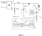
- FIG. 2 is a circuit diagram showing a detailed structure of the LED drive circuit according to the embodiment of the present disclosure.
- the LED drive circuit according to the present embodiment includes the silicon-controlled rectifier dimmer TRIAC, a bleeder circuit 1, the linear drive circuit 2, a control circuit 3, and the rectification circuit 4.
- the silicon-controlled rectifier dimmer TRIAC is connected between the rectification circuit 4 and an alternating current input terminal to chop an alternating current input voltage.
- the rectification circuit 4 is configured to convert the alternating current input voltage into a direct current bus voltage VBUS at a terminal of the direct current bus.
- the bleeder circuit 1 is connected between a direct current voltage bus and a ground terminal to form a current path substantially in parallel with an LED load.
- the bleeder circuit 1 is used to sink a bleeder current from the direct current bus and continuously maintain the operation of the silicon-controlled rectifier dimmer TRIAC.
- the control circuit 3 and the bleeder circuit 1 form the bus voltage adjustment circuit X.
- the control circuit 3 is configured to acquire a conduction angle signal of the silicon-controlled rectifier dimmer and control a bleeder current of the bleeder circuit 1, to adjust the direct current bus voltage and delay the turn-on time instant of the silicon-controlled rectifier dimmer. Specifically, the control circuit 3 is configured to adjust the direct current bus voltage in the case that the conduction angle signal is greater than the angle threshold, so that the direct current bus voltage VBUS when the silicon-controlled rectifier dimmer is turned on is near a preset lighting voltage VLED, for example, is slightly less than or slightly greater than the lighting voltage VLED.
- the direct current bus voltage VBUS when the silicon-controlled rectifier dimmer is turned on is controlled so that the absolute value of the difference between the direct current bus voltage VBUS and the lighting voltage VLED is small, to reduce the power loss of the LED drive circuit.
- the absolute value of the difference between the direct current bus voltage VBUS and the lighting voltage VLED may range from 0V to 30V.
- the bleeder current can be dynamically controlled based on the conduction angle signal to adjust the turn-on time instant of the silicon-controlled rectifier dimmer TRIAC, so that the time period during which it is still required to sink the bleeder current after the silicon-controlled rectifier dimmer TRIAC is turned on and the energy required for the bleeding can be decreased as much as possible, thereby reducing loss as much as possible.
- the direct current bus voltage VBUS may be adjusted to be not less than the preset lighting voltage VLED.
- the conduction angle is defined as an angle indicating a conduction period of the silicon-controlled rectifier dimmer in an operation period.
- the conduction angle signal is used to indicate the conduction period or the conduction angle.
- control circuit 3 is configured to adjust a desired value of the direct current bus voltage VBUS during bleeding process so that the direct current bus voltage VBUS when the silicon-controlled rectifier dimmer TRIAC is turned on is slightly greater than the preset lighting voltage VLED.
- the bleeder current can be dynamically controlled based on the conduction angle signal to adjust the turn-on time instant, so that it is not required to sink the bleeder current after the silicon-controlled rectifier dimmer TRIAC is turned on, thereby reducing the power loss as much as possible.
- control circuit 3 is configured to control the desired value of the direct current bus voltage to change with the conduction angle signal in the case that the conduction angle signal is greater than the angle threshold, and control the desired value of the direct current bus voltage to be a preset value in a case that the conduction angle signal is less than the angle threshold.
- the preset value corresponds to a direct current bus voltage corresponding to the maximum conduction angle, and may be zero or greater than zero.
- the desired value is adjusted by adjusting a reference voltage CV REF used by the control circuit 3 to control the bleeding process.
- the reference voltage CV REF is used to indicate the desired value.
- CV REF denotes the reference voltage
- Vcd denotes the conduction angle signal
- Vcd_ref denotes the angle threshold
- CV REF_MIN denotes a reference voltage corresponding the preset value
- the angle threshold corresponds to the conduction angle signal when the direct current bus voltage is equal to the preset lighting voltage at the turn-on time instant of the silicon-controlled rectifier dimmer
- K denotes a preset adjustment coefficient.
- the angle threshold is set to meet the following rule: for alternating current input power with commonly used parameters (e.g., the alternating current power of 220V and 50Hz), in a case that the silicon-controlled rectifier dimmer performs chopping at a conduction angle equal to the angle threshold, the voltage obtained by the chopping is equal to or slightly greater than the lighting voltage VLED.
- the direct current bus voltage at the turn-on time instant is greater than the lighting voltage VLED if the conduction angle signal is less than the angle threshold, and the direct current bus voltage at the turn-on time instant is less than the lighting voltage VLED if the conduction angle signal is greater than the angle threshold, but still have a higher value.
- the bleeder circuit sinks the bleeder current from a high direct current bus voltage, which should be avoided by control.
- the reference voltage CV REF for indicating the desired value of the direct current bus voltage is set to change with the conduction angle signal Vcd, as shown in above formula. Therefore, the direct current bus voltage can be raised as the conduction angle signal increases, to delay the turn-on time instant of the silicon-controlled rectifier dimmer TRIAC, so that the direct current bus voltage at the turn-on time instant is raised to be a voltage greater than or slightly greater than the lighting voltage VLED.
- the conduction angle signal may be acquired in various ways.
- the conduction angle signal may be acquired by detecting the direct current bus voltage VBUS.
- the conduction angle signal may be acquired by detecting a time period from a time instant when the direct current bus voltage VBUS rises to a voltage greater than a first threshold to a time instant when the direct current bus voltage VBUS decreases to a voltage less than a second threshold in an operation period.
- the conduction angle signal may be acquired by detecting a drive current of the LED load.
- the conduction angle signal may be acquired by detecting a time period during which the drive current is continuously greater than a third threshold.
- the control circuit 3 forms a voltage feedback loop based on a direct current bus voltage sampling signal VBUS1, to control the direct current bus voltage VBUS to change in a desired way before the silicon-controlled rectifier dimmer TRIAC is turned on.
- the direct current bus voltage sampling signal VBUS1 may be obtained by performing sampling with a resistor voltage divider network arranged between the direct current bus and the ground terminal.
- the control circuit 3 may turn off the bleeder circuit when it is detected that the silicon-controlled rectifier dimmer TRIAC is turned on or the direct current bus voltage VBUS rises to a voltage greater than the lighting voltage VLED.
- FIG. 2 shows the detailed structure of the LED drive circuit according to the embodiment of the present disclosure.
- the bleeder circuit 1 includes a transistor Q1.
- the linear drive circuit 2 includes a transistor Q2, and is used to control a drive current flowing through the LED load to maintain the drive current substantially constant.
- the LED drive circuit according to this embodiment may further include a diode D1 connected between the bleeder circuit and the LED load and a filter capacitor Co connected in parallel with the LED load. It should be understood that the diode D1 may be omitted or replaced with other unidirectional circuits.
- the bleeder circuit 1 and the linear drive circuit 2 may further be provided with resistors to sample the flowed bleeder current or drive current. The resistors may be arranged in a manner different from that shown Figure 2 .
- the control circuit 3 may include a detection circuit 31, a reference voltage setting circuit 32, and a bleeding controller 33.
- the detection circuit 31 is used to acquire the conduction angle signal Vcd.
- the reference voltage setting circuit 32 is configured to set the reference voltage CV REF based on the conduction angle signal in the described-above manner to adjust the desired value of the direct current bus voltage.
- the bleeding controller 33 is used to control the bleeder current of the bleeder circuit 1 based on the reference voltage CV REF and the direct current bus voltage sampling signal VBUS1, so that the direct current bus voltage VBUS changes with the desired value indicated by the reference voltage CV REF . Specifically, the bleeding controller 33 generates a control signal to control the transistor Q1, so as to adjust a current IQ1 flowing through the transistor Q1.
- FIG. 3 is a circuit diagram showing an implementation of a detection circuit according to the embodiment of the present disclosure.
- the detection circuit 31 acquires the conduction angle signal by detecting the direct current bus voltage VBUS.
- the detection circuit 31 is configured to acquire a signal for indicating a time period from a time instant when the direct current bus voltage VBUS rises to a voltage greater than a first threshold to a time instant when the direct current bus voltage VBUS decreases to a voltage less than a second threshold, in order to acquire the conduction angle signal.
- the first threshold may be set to an integer multiple of the second threshold, so as to better reuse a voltage source.
- the detection circuit 31 includes comparators CMP1 and CMP2, one-shot circuits OS1 and OS2, a RS trigger RS1, a voltage source VDD, switches S1 and S2, a resistor Rd, and a capacitor Cd. Other components in the circuit than the capacitor Cd may be implemented by an integrated circuit.
- One input terminal of the comparator CMP1 is applied with the direct current bus voltage sampling signal VBUS1 for indicating the direct current bus voltage VBUS
- the other input terminal of the comparator CMP1 is applied with a threshold V1
- an output terminal of the comparator CMP1 is connected to an input terminal of the one-shot circuit OS1.
- An output terminal of the one-shot circuit OS1 is connected to a set terminal of the RS trigger RS1.
- the one-shot circuit OS1 may generate a pulse having a preset time length in response to a rising or falling edge of an input signal to set the output signal of the RS trigger RS1.
- One input terminal of the comparator CMP2 is applied with the direct current bus voltage sampling signal VBUS1, the other input terminal of the comparator CMP2 is applied with a threshold V2, and an output terminal of the comparator CMP2 is connected to an input terminal of the one-shot circuit OS2.
- An output terminal of the one-shot circuit OS2 is connected to a reset terminal of the RS trigger RS1.
- the one-shot circuit OS2 may generate a pulse having a preset time length in response to a rising or falling edge of an input signal to reset the output signal of the RS trigger RS1.
- a state controller 31a controls a charge and discharge circuit 31b to switch to a first state when it is detected that the direct current bus voltage VBUS rises to a voltage greater than the first threshold, and controls the charge and discharge circuit 31b to switch to a second state when it is detected that the direct current bus voltage VBUS decreases to a voltage less than the second threshold.
- the first threshold corresponds to the threshold V1
- the second threshold corresponds to the threshold V2.
- the switches S1 and S2 are connected in series between a positive terminal of the voltage source VDD and a ground terminal.
- the switch S1 is controlled by an output signal Q of the RS trigger, and the switch S2 is controlled by an inverting signal of the signal Q.
- the switch S1 and the switch S2 are in opposite states.
- the resistor Rd and the capacitor Cd are connected in series between a common connection terminal of the switch S1 and the switch S2 and the ground terminal.
- the switch S1 is turned on
- the switch S2 is turned off, and the capacitor Cd is charged.
- the switch S1 is turned off
- the switch S2 is turned on, and the capacitor Cd is discharged through the resistor Rd and the switch S2.
- a charge and discharge circuit 31b is formed.
- the charge and discharge circuit 31b charges the capacitor Cd in the first state and discharges the capacitor Cd in the second state under control of the state controller.
- the resistor Rd and the capacitor Cd form an RC circuit, which leads to hysteresis on the change of a voltage Vcd across the capacitor Cd due to the existence of the resistor Rd.
- the voltage Vcd slowly changes with the conduction angle. Since the voltage Vcd changes little in an operation period, the voltage Vcd at any one time instant in the operation period may serve as the conduction angle signal. Since the capacitor is conductive with respect to an instantaneous voltage (the capacitor has almost no resistance), an instantaneous current is quite large when the capacitor is directly connected to the voltage source VDD, which results in a charging-end component easily being burned. Therefore, the resistor is connected in series with the capacitor so as to limit a maximum current.
- Figure 4 is an operation waveform diagram of the detection circuit shown in Figure 3 .
- the voltage VBUS1 rises with the direct current bus voltage to a voltage greater than the threshold V1.
- the voltage VBUS1 decreases with the direct current bus voltage to a voltage less than the threshold V2.
- the voltage Vcd changes slowly in one operation period, and may indicate the time period ton from a time instant when the silicon-controlled rectifier dimmer is turned on to a time instant when the operation period substantially ends.
- connection manner of the input terminal of the comparator, the trigger manner of the one-shot circuit, and the connection relation of the RS trigger may be adjusted based on the set of a valid level and the relation manner of the input signal.
- FIG. 5 is a circuit diagram showing another implementation of the detection circuit according to the embodiment of the present disclosure.
- the detection circuit 31 is configured to acquire a signal for indicating a time period during which the drive current is continuously greater than a third threshold to acquire the conduction angle signal.
- the detection circuit 31 includes a comparator CMP3, a voltage source VDD, switches S3 and S4, a resistor Rd, and a capacitor Cd.
- One input terminal of the comparator CMP3 receives a current sampling signal Vs, and the other input terminal of the comparator CMP3 is applied with a threshold VSET.
- the threshold VSET corresponds to a fourth threshold.
- the switches S3 and S4 are connected in series between a positive terminal of the voltage source VDD and a ground terminal.
- the switch S3 is controlled by an output signal of the comparator CMP3, and the switch S4 is controlled by an inverting signal of the output signal of the comparator CMP3.
- the switch S3 and the switch S4 are in opposite states.
- the resistor Rd and the capacitor Cd are connected in series between a common connection terminal of the switch S3 and the switch S4 and the ground terminal.
- the current sampling signal Vs is greater than the threshold VSET
- the comparator CMP3 outputs a high level
- the switch S3 is turned on
- the switch S4 is turned off
- the voltage source VDD charges the capacitor Cd through the switch S3 and the resistor Rd.
- the current sampling signal Vs is less than the threshold VSET
- the comparator CMP3 outputs a low level
- the switch S3 is turned off
- the switch S4 is turned on
- the capacitor Cd is discharged through the resistor Rd and the switch S4. Due to the resistor Rd, a voltage Vcd across the capacitor Cd changes slowly in an operation period, and may be used to indicate the time period ton during which the LED load operates, which corresponds directly to the conduction angle, as shown in Figure 6 . Therefore, the voltage Vcd in this implementation may serve as the conduction angle signal.
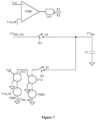
- FIG. 7 is a circuit diagram showing a reference voltage setting circuit according to the embodiment of the present disclosure.
- the reference voltage setting circuit 32 includes a comparator CMP4, a logic circuit LG1, switches S5 and S6, voltage sources VDD1 and VDD2, controlled voltage sources CV1 and CV2, and a capacitor Cr.
- One input terminal of the comparator CMP4 receives the conduction angle signal Vcd, and the other input terminal of the comparator CMP4 receives the angle threshold Vcd_ref.
- the logic circuit LG1 outputs a non-inverting signal K1 and an inverting signal K2 of an output signal of the comparator CMP4.
- the switch S5 is controlled by the signal K1.
- the switch S6 is controlled by the signal K2.
- the switch S6 is used to control a path from a preset value (of a voltage signal) CV REF_MIN to the capacitor Cr.
- the switch S5 is used to control a path from a voltage expressed as (Vcd-Vcd_ref) *K+CV REF_MIN to the capacitor Cr. Since the control signals for the switches S5 and S6 are inverted, only one of the two voltage signals is introduced to the capacitor Cr. Further, a circuit formed by the voltage sources VDD1 and VDD2 and the controlled voltage sources CV1 and CV2 is controlled by the conduction angle signal Vcd, and generates the output voltage (Vcd-Vcd_ref) *K+CV REF_MIN . The voltage across the capacitor Cr is outputted as a reference voltage CV REF .
- the capacitor Cr is used to cause the reference voltage CV REF to change smoothly when being switched. Therefore, in a case that the conduction angle signal Vcd is less than the angle threshold Vcd_ref, the comparator CMP4 outputs a low level, the switch S6 is turned on, the switch S5 is turned off, and the reference voltage setting circuit 32 outputs the reference voltage CV REF_MIN corresponding to the preset value (of the voltage signal) as the reference voltage CV REF .
- the comparator CMP4 outputs a high level, the switch S6 is turned off, the switch S5 is turned on, and the reference voltage setting circuit 32 outputs the voltage (Vcd-Vcd_ref) *K+CV REF_MIN as the reference voltage CV REF .
- FIG 8 is a circuit diagram showing a bleeder circuit and a bleeding controller according to the embodiment of the present disclosure.
- the bleeder circuit 1 includes a transistor Q1, and a maximum current clamp circuit 11.
- the maximum current clamp circuit 11 and the transistor Q1 are connected in series between the direct current bus and the ground terminal.
- the maximum current clamp circuit 11 serves as a protection circuit for limiting a maximum value of a current. Since the maximum current clamp circuit 11 is arranged on the bleeding path, it is used to limit a maximum value of the bleeder current. That is, in a case that the bleeder current IQ1 is less than a clamp current IMAX, the maximum current clamp circuit 11 is in a shoot-through state. When the bleeder current IQ1 rises to the clamp current IMAX, the maximum current clamp circuit 11 clamps the bleeder current to maintain the bleeder current IQ1 at the clamp current IMAX.
- the bleeding controller 33 includes an error amplifier EA3.
- One input terminal of the error amplifier EA3 receives the direct current bus voltage sampling signal VBUS1, the other input terminal of the error amplifier EA3 receives the reference voltage CV REF , and an output terminal of the error amplifier EA3 outputs a control signal to control the operation state of the transistor Q1.
- a voltage feedback loop is formed, and the direct current bus voltage is maintained to correspond to the reference voltage CV REF by adjusting the bleeder current.
- the bleeding controller 33 can regulate the bleeder current in accordance with an error between the reference voltage CV REF and the direct current bus voltage sampling signal VBUS1 to maintain the direct current bus voltage equal to the desired value.
- the reference voltage CV REF increases with the conduction angle signal, so that the bus voltage sampling signal VBUS1 is adjusted to be increased, and then the direct current bus voltage VBUS is increased.
- the maximum current clamp circuit 11 includes a transistor Q3, a voltage source V3, a resistor RL, and a switch S7.
- the voltage source V3 is connected between a control terminal of the transistor Q3 and the ground terminal.
- the switch S7 is connected between a gate of transistor Q3 and the ground terminal. The switch S7 is controlled by an enable signal CV_EN.
- the enable signal CV_EN is used to indicate the operation state of the control circuit 3, i.e., detecting an operation time period before the silicon-controlled rectifier dimmer TRIAC is turned on, so as to effectively protect the bleeder circuit 1.
- the enable signal CV_EN is a low level, it is indicated that the silicon-controlled rectifier dimmer TRIAC is already turned on, the control circuit 3 no longer adjusts the direct current bus voltage VBUS, the switch S7 is turned on, a gate voltage of the transistor Q3 is pulled down to zero, the transistor Q3 is turned off, the maximum current clamp circuit 11 exits the protection state, and the bleeder circuit 1 does not sink the bleeder current any longer.
- the enable signal CV_EN is a high level
- the control circuit 3 adjusts the direct current bus voltage VBUS
- the switch S7 is turned off
- the transistor Q3 enters the protection state under control of the voltage source V3.
- the maximum current clamp circuit may also be implemented by other structures, and the state of the bleeder circuit may be controlled in other manners.
- a switch controlled by the enable signal CV_EN is connected to the gate of the transistor Q1 to control the bleeder circuit.
- FIG 9 is a circuit diagram showing an enable signal generating circuit for controlling the maximum current clamp circuit according to the embodiment of the present disclosure.
- An enable signal generating circuit 33a may serves as a part of the bleeding controller 33 or may be a separate circuit module.
- the enable signal generating circuit 33a includes comparators CMP5 to COM7, one-shot circuits OS3 to OS5, an AND gate AND, and an RS trigger RS2.
- the comparator CMP5 is used to compare the direct current bus voltage sampling signal VBUS1 with a threshold Vth1.
- the one-shot circuit OS3 is used to output a pulse signal having a preset length in response to a rising edge or a falling edge of an output signal of the comparator CMP5.
- the comparator CMP6 is used to compare the direct current bus voltage sampling signal VBUS1 with a threshold Vth2.
- the one-shot circuit OS4 is used to output a pulse signal having a preset length in response to a rising edge or a falling edge of an output signal of the comparator CMP6.
- Two input terminals of the AND gate AND are connected to output terminals of the one-shot circuits OS3 and OS4, respectively, and an output terminal of the AND gate AND is connected to a reset terminal of the RS trigger RS2.
- the comparator CMP7 is used to compare the direct current bus voltage sampling signal VBUS1 with a threshold Vth3.
- the one-shot circuit OSS is used to output a pulse signal having a preset length in response to a rising edge or a falling edge of an output signal of the comparator CMP7.
- An output terminal of the one-shot circuit OSS is connected to a set terminal of the RS trigger RS2.
- FIG 10 is an operation waveform diagram of the LED drive circuit according to the embodiment of the present disclosure.
- the waveforms of the VBUS and IQ1 with solid lines are operation waveforms in a case that the direct current bus voltage VBUS before the silicon-controlled rectifier dimmer TRIAC is turned on is set to a constant voltage, and the waveforms of the VBUS and IQ1 with dotted lines are waveforms obtained by performing controlling according to the embodiment of the present disclosure.
- the direct current bus voltage sampling signal VBUS 1 is less than the threshold Vth3, and thus a pulse signal is triggered to set the RS trigger RS2.
- the enable signal CV_EN switches to a high level, which indicates that the silicon-controlled rectifier dimmer TRIAC is turned off.
- the enable signal CV_EN controls the maximum current clamp circuit to enter the protection state, and the bleeding controller 33 performs constant voltage control based on the conduction angle signal Vcd, so that the direct current bus voltage corresponds to the reference voltage CV REF . If the silicon-controlled rectifier dimmer TRIAC is turned on, the direct current bus voltage VBUS rises rapidly.
- the direct current bus voltage sampling signal VBUS1 successively rises to a value greater than the threshold Vth1 and a value greater than the threshold Vth2 in a short time period, to trigger two pulse signals, respectively.
- the AND gate AND may output a pulse signal to reset the RS trigger RS2.
- the enable signal CV_EN switches to a low level, which indicates that the silicon-controlled rectifier dimmer TRIAC is turned on.
- the enable signal CV_EN controls the maximum current clamp circuit to exit the protection state, and the direct current bus voltage increases with the input voltage, rather than under the constant voltage control. In this way, the operation state of the silicon-controlled rectifier dimmer TRIAC can be effectively detected.
- the enable signal generating circuit 33a may also be implemented by other logic circuits.
- the direct current bus voltage VBUS is in a constant voltage state by controlling the bleeder circuit according to the embodiment of the present disclosure.
- the desired value of the direct current bus voltage is adjustable. In the case that the conduction angle is large, the desired value is controlled to be increased so as to delay the turn-on time instant. In this way, the direct current bus voltage VBUS when the silicon-controlled rectifier dimmer TRIAC is turned on can be near the lighting voltage VLED by performing controlling, no matter how the conduction angle of the silicon-controlled rectifier dimmer changes, and how properties of the silicon-controlled rectifier dimmer change.
- the bleeder current of the circuit has a small pulse only in a short time period after the silicon-controlled rectifier dimmer is turned on, and remains low in other time periods than the short time period, which avoids the circuit loss caused by the fact that the bleeder circuit is required to sink the bleeder current before and after the silicon-controlled rectifier dimmer is turned on. Therefore, with the embodiment of the present disclosure, the loss of the bleeder circuit can be reduced, and the system efficiency can be improved.
- the bleeder circuit 1 and the control circuit 3 according to the present embodiment may form a circuit module.
- the circuit module may be used in combination with various silicon-controlled rectifier dimmers, rectification circuits and linear drive circuits to form dimmable LED drive circuits.
- the circuit module according to the embodiment of the present disclosure is used in combination with various silicon-controlled rectifier dimmers having different maximum conduction angles, high efficiency and low loss can be achieved.
- FIG 11 is a flowchart showing a control method for controlling an LED drive circuit according to an embodiment of the present disclosure, which is not covered by the appended claims.
- a direct current bus voltage is adjusted to delay a turn-on time instant of the silicon-controlled rectifier dimmer.
- the direct current bus voltage is increased so that an absolute value of a difference between the direct current bus voltage when the silicon-controlled rectifier dimmer is turned on and a preset lighting voltage of an LED load is in a preset range.
- the direct current bus voltage is controlled to be maintained at a first voltage, where the first voltage is set so that an absolute value of a difference between the direct current bus voltage when the silicon-controlled rectifier dimmer is turned on and a preset lighting voltage of an LED load is in a preset range.
- the direct current bus voltage is increased so that the direct current bus voltage when the silicon-controlled rectifier dimmer is turned on is not less than a preset lighting voltage of an LED load.
- control method includes the following steps S100 and S200.
- step S100 a conduction angle signal for indicating a conduction angle of the silicon-controlled rectifier dimmer is acquired.
- step S200 a desired value of the direct current bus voltage is adjusted based on the conduction angle signal.
- step S200 may be performed by:
- the desired value is controlled to change with the conduction angle signal.
- the desired value is controlled to be a preset value equal to or greater than zero.
- CV REF Vcd ⁇ Vcd_ref ⁇ K + CV REF_MIN
- CV REF denotes the reference voltage
- Vcd denotes the conduction angle signal
- Vcd_ref denotes the angle threshold
- CV REF_MIN denotes a reference voltage corresponding the preset value
- the angle threshold is set to correspond to the conduction angle signal when the direct current bus voltage is equal to the preset lighting voltage during the conduction of the silicon-controlled rectifier dimmer
- K denotes a preset adjustment coefficient.
- step S100 may be performed by: detecting the direct current bus voltage to acquire the conduction angle signal of the silicon-controlled rectifier dimmer; or detecting a drive current of an LED load to acquire the conduction angle signal.
- the detecting the direct current bus voltage to acquire the conduction angle signal of the silicon-controlled rectifier dimmer includes: acquiring a signal for indicating a time period from a time instant when the direct conduction angle signal.
- the detecting a drive current of an LED load to acquire the conduction angle signal includes: acquiring a signal for indicating a time period during which the drive current is continuously greater than a third threshold to acquire the conduction angle signal.
- the direct current bus voltage during the bleeding is controlled to be constant, and the desired value of the direct current bus voltage is adjustable, so that the turn-on time instant can be delayed in the case that the conduction angle is large, and the direct current bus voltage can rapidly rise to a voltage greater than the lighting voltage when the silicon-controlled rectifier dimmer is turned on. In this way, it is not required to sink the bleeder current for a long time period after the silicon-controlled rectifier dimmer is turned on, effectively reducing the system loss, and improving the system efficiency.
Landscapes
- Circuit Arrangement For Electric Light Sources In General (AREA)
Description
- The present disclosure relates to power electronic technology, in particular to light emitting diode (LED) drive circuit technology, and particularly to a circuit module, a dimmable LED drive circuit and a control method.
- At present, the silicon-controlled rectifier dimming is a commonly used dimming method. A phase control method is adopted by a silicon-controlled rectifier dimmer TRIAC to perform dimming, that is, the silicon-controlled rectifier dimmer is controlled to be turned on in each half cycle of the sinusoidal wave to acquire the same conduction phase angle. By adjusting the chopper phase of the silicon-controlled rectifier dimmer, the conduction phase angle can be changed to perform dimming.
- In the conventional technology, the silicon-controlled rectifier dimmer is generally combined with the linear constant current control. The linear constant current control is implemented by controlling a linear device (for example, a transistor in a linear state) substantially connected in series with at least a part of an LED load to adjust the current flowing through the LED load so as to maintain the current constant. A time period during which the silicon-controlled rectifier dimmer is turned on in an operation period (which usually is a half-wave period of the alternating current) may be indicated by a conduction angle. Further, it is required to sink a bleeder current from the direct current bus, so as to ensure the operation of the silicon-controlled rectifier dimmer. In a case that the conduction angle of the silicon-controlled rectifier dimmer is large, the direct current bus voltage when the silicon-controlled rectifier dimmer is turned on is less than the lighting voltage of the LED load, and the LED load still does not operate. In this case, the bleeder circuit is required to sink a large current until the direct current bus voltage rises to the lighting voltage, which results in a large circuit loss, and greatly reduces system efficiency. Further, the temperature of the circuit is increased due to the heat generated by the bleeder circuit, which further affects the system performance.
CN 106888524 A discloses an LED drive circuit having a silicon controlled rectifier regulator, a circuit module, and a control method. Before conduction of a silicon controlled rectifier regulator, a direct-current bus voltage is controlled by a bleeder circuit to change in a predetermined manner, so that a phenomenon that conduction points of the silicon controlled rectifier regulators are affected because of inconformity of leakage currents due to different types of the silicon controlled rectifier regulators and different circuit setting and thus a problem of LED scintillation can be solved. Meanwhile, with control of the direct-current bus voltage, the voltage of the silicon controlled rectifier regulator after conduction can be affected, so that the voltage of the conduction point can be set flexibly based on needs.
US 2013/343090 A1 discloses an active bleeder according to an exemplary embodiment of the present invention includes a bleed switch coupled to the input voltage and an active bleeding controller generating a bleed reference voltage according to a result of counting a period during which the input voltage is generated and switching the bleed switch according to a result of comparison between the bleed reference voltage and a bleed sense voltage corresponding to a current flowing to the bleed switch.
However,CN 106888524 A andUS 2013/343090 A1 cannot greatly improve system efficiency effectively, and the temperature of the circuit is still increased due to the heat generated by the bleeder circuit, which further affects the system performance. - In view of this, there are provided a circuit module, a dimmable LED drive circuit, and a control method according to embodiments of the present disclosure, to effectively reduce system loss and improve system efficiency. The disclosure is defined by the independent claim. The dependent claims define embodiments.
- With the technical solutions according to the embodiments of the present disclosure, the direct current bus voltage during the bleeding is controlled to be constant, and the desired value of the direct current bus voltage is adjustable, so that the turn-on time instant can be delayed in the case that the conduction angle is large, and the direct current bus voltage when the silicon-controlled rectifier dimmer is turned on can be near a lighting voltage. In this way, it is not required to sink the bleeder current from the direct current bus for a long time period after the silicon-controlled rectifier dimmer is turned on, effectively reducing the system loss, and improving the system efficiency.
- The above and other objects, features, and advantages of the present disclosure are clearer from the following description of embodiments of the present disclosure with reference to the drawings. In the drawings:
-
Figure 1 is a circuit diagram showing an LED drive circuit according to an embodiment of the present disclosure; -
Figure 2 is a circuit diagram showing a detailed structure of the LED drive circuit according to the embodiment of the present disclosure; -
Figure 3 is a circuit diagram showing an implementation of a detection circuit according to the embodiment of the present disclosure; -
Figure 4 is an operation waveform diagram of the detection circuit shown inFigure 3 ; -
Figure 5 is a circuit diagram showing another implementation of the detection circuit according to the embodiment of the present disclosure; -
Figure 6 is an operation waveform diagram of the detection circuit shown inFigure 5 ; -
Figure 7 is a circuit diagram showing a reference voltage setting circuit according to the embodiment of the present disclosure; -
Figure 8 is a circuit diagram showing a bleeder circuit and a bleeding controller according to the embodiment of the present disclosure; -
Figure 9 is a circuit diagram showing an enable signal generating circuit for controlling a clamp circuit according to the embodiment of the present disclosure; -
Figure 10 is an operation waveform diagram of the LED drive circuit according to the embodiment of the present disclosure; and -
Figure 11 is a flowchart showing a control method for controlling an LED drive circuit according to an embodiment of the present disclosure, which is not covered by the appended claims. - The present disclosure is described below based on embodiments, and the present disclosure is not limited to the embodiments. In the following description of the present disclosure, specific details are described in detail. The present disclosure can be fully understood by those skilled in the art without the description of these details. Well-known methods, processes, flows, components and circuits are not described in detail to avoid obscuring the essence of the present disclosure.
- Further, it should be understood by those skilled in the art that, the drawings herein are only for illustration, and the drawings are not necessarily drawn to scale.
- It should further be understood that in the following description, a "circuit" indicates a conductive loop formed by at least one component or sub-circuit by electrical connection or electromagnetic connection. In a case that a component or circuit is described as being "connected to" another component or being "connected" between two nodes, the component or circuit may be coupled or connected to another component directly or via an intermediate component. The connection between the two components may be physical connection, logical connection, or a combination thereof. In addition, in a case that the component is described as being "directly coupled to" or "directly connected to" another component, it indicates that no intermediate component exists between the two components.
- Unless otherwise indicated in the context, the words "including", "comprising", and the like, in the specification and the claims, should be interpreted as being inclusive rather than being exclusive or exhaustive, i.e., "including but not limited to".
- In the description of the present disclosure, it should be understood that, the terms "first", "second", and the like are used only for descriptive purposes and are not to be construed as indicating or implying relative importance. In addition, in the present disclosure, the word "multiple" indicates two or more unless otherwise specified.
- It is found that, in a case that a conduction angle of a silicon-controlled rectifier dimmer TRIAC is large, a bleeder circuit sinks a bleeder current from a direct current bus to provide a turn-on current before the silicon-controlled rectifier dimmer TRIAC is turned on. Due to the large conduction angle, a direct current bus voltage VBUS when the silicon-controlled rectifier dimmer TRIAC is turned on is lower than a lighting voltage VLED, and the bleeder circuit is required to continue to sink the bleeder current to provide a holding current, so as to ensure that the silicon-controlled rectifier dimmer TRIAC can be effectively turned on. In the case that the conduction angle of the silicon-controlled rectifier dimmer TRIAC is large, the direct current bus voltage VBUS can be controlled at a desired value to be constant before the silicon-controlled rectifier dimmer TRIAC is turned on, in order to reduce a time period of the bleeder current. However, one disadvantage of this approach is that, the desired value of the direct current bus voltage VBUS cannot be changed for different conduction angles, the bleeder current need be provided until the direct current bus voltage VBUS rises to be greater than the lighting voltage VLED, which results in a large circuit loss, and greatly reduces system efficiency. Further, the temperature of the circuit is increased due to the heat generated by the bleeder circuit, which further affects the system performance.
-
Figure 1 is a circuit diagram showing an LED drive circuit according to an embodiment of the present disclosure. As shown inFigure 1 , the LED drive circuit according to the present embodiment includes a silicon-controlled rectifier dimmer TRIAC, alinear drive circuit 2, arectification circuit 4, and a bus voltage adjustment circuit X. The bus voltage adjustment circuit X is configured to adjust a direct current bus voltage to delay a turn-on time instant of the silicon-controlled rectifier dimmer in a case that a conduction angle signal is greater than an angle threshold. - Specifically, the bus voltage adjustment circuit X is configured to increase the direct current bus voltage in the case that the conduction angle signal is greater than the angle threshold, so that an absolute value of a difference between the direct current bus voltage when the silicon-controlled rectifier dimmer is turned on and a preset lighting voltage of an LED load is in a preset range.
- Specifically, the bus voltage adjustment circuit X is configured to control the direct current bus voltage to be maintained at a first voltage in the case that the conduction angle signal is greater than the angle threshold, where the first voltage is set so that the absolute value of the difference between the direct current bus voltage when the silicon-controlled rectifier dimmer is turned on and the preset lighting voltage of the LED load is in the preset range. The first voltage is set based on the conduction angle signal. A large conduction angle signal corresponds to a large first voltage, to ensure that the direct current bus voltage when the silicon-controlled rectifier dimmer is turned on is near the lighting voltage, so that the absolute value of the difference between the direct current bus voltage and the lighting voltage is in the preset range. The preset range is determined by the demands of application environments.
- Specifically, the bus voltage adjustment circuit X is configured to increase the direct current bus voltage to delay the turn-on time instant of the silicon-controlled rectifier dimmer in the case that the conduction angle signal is greater than the angle threshold, so that the direct current bus voltage when the silicon-controlled rectifier dimmer is turned on is not less than the preset lighting voltage of the LED load.
-
Figure 2 is a circuit diagram showing a detailed structure of the LED drive circuit according to the embodiment of the present disclosure. As shown inFigure 2 , the LED drive circuit according to the present embodiment includes the silicon-controlled rectifier dimmer TRIAC, ableeder circuit 1, thelinear drive circuit 2, acontrol circuit 3, and therectification circuit 4. The silicon-controlled rectifier dimmer TRIAC is connected between therectification circuit 4 and an alternating current input terminal to chop an alternating current input voltage. Therectification circuit 4 is configured to convert the alternating current input voltage into a direct current bus voltage VBUS at a terminal of the direct current bus. Thebleeder circuit 1 is connected between a direct current voltage bus and a ground terminal to form a current path substantially in parallel with an LED load. Thebleeder circuit 1 is used to sink a bleeder current from the direct current bus and continuously maintain the operation of the silicon-controlled rectifier dimmer TRIAC. - The
control circuit 3 and thebleeder circuit 1 form the bus voltage adjustment circuit X. - The
control circuit 3 is configured to acquire a conduction angle signal of the silicon-controlled rectifier dimmer and control a bleeder current of thebleeder circuit 1, to adjust the direct current bus voltage and delay the turn-on time instant of the silicon-controlled rectifier dimmer. Specifically, thecontrol circuit 3 is configured to adjust the direct current bus voltage in the case that the conduction angle signal is greater than the angle threshold, so that the direct current bus voltage VBUS when the silicon-controlled rectifier dimmer is turned on is near a preset lighting voltage VLED, for example, is slightly less than or slightly greater than the lighting voltage VLED. The direct current bus voltage VBUS when the silicon-controlled rectifier dimmer is turned on is controlled so that the absolute value of the difference between the direct current bus voltage VBUS and the lighting voltage VLED is small, to reduce the power loss of the LED drive circuit. For example, the absolute value of the difference between the direct current bus voltage VBUS and the lighting voltage VLED may range from 0V to 30V. Thus, the bleeder current can be dynamically controlled based on the conduction angle signal to adjust the turn-on time instant of the silicon-controlled rectifier dimmer TRIAC, so that the time period during which it is still required to sink the bleeder current after the silicon-controlled rectifier dimmer TRIAC is turned on and the energy required for the bleeding can be decreased as much as possible, thereby reducing loss as much as possible. - In one embodiment, the direct current bus voltage VBUS may be adjusted to be not less than the preset lighting voltage VLED. The conduction angle is defined as an angle indicating a conduction period of the silicon-controlled rectifier dimmer in an operation period. The conduction angle signal is used to indicate the conduction period or the conduction angle.
- Further, the
control circuit 3 is configured to adjust a desired value of the direct current bus voltage VBUS during bleeding process so that the direct current bus voltage VBUS when the silicon-controlled rectifier dimmer TRIAC is turned on is slightly greater than the preset lighting voltage VLED. Thus, the bleeder current can be dynamically controlled based on the conduction angle signal to adjust the turn-on time instant, so that it is not required to sink the bleeder current after the silicon-controlled rectifier dimmer TRIAC is turned on, thereby reducing the power loss as much as possible. - In another embodiment, the
control circuit 3 is configured to control the desired value of the direct current bus voltage to change with the conduction angle signal in the case that the conduction angle signal is greater than the angle threshold, and control the desired value of the direct current bus voltage to be a preset value in a case that the conduction angle signal is less than the angle threshold. The preset value corresponds to a direct current bus voltage corresponding to the maximum conduction angle, and may be zero or greater than zero. Specifically, the desired value is adjusted by adjusting a reference voltage CVREF used by thecontrol circuit 3 to control the bleeding process. The reference voltage CVREF is used to indicate the desired value. In the case that the conduction angle signal is greater than the angle threshold, the reference voltage may be set according to the following formula:

where CVREF denotes the reference voltage, Vcd denotes the conduction angle signal, Vcd_ref denotes the angle threshold, CVREF_MIN denotes a reference voltage corresponding the preset value, the angle threshold corresponds to the conduction angle signal when the direct current bus voltage is equal to the preset lighting voltage at the turn-on time instant of the silicon-controlled rectifier dimmer, and K denotes a preset adjustment coefficient. - That is, in the above embodiment, the angle threshold is set to meet the following rule: for alternating current input power with commonly used parameters (e.g., the alternating current power of 220V and 50Hz), in a case that the silicon-controlled rectifier dimmer performs chopping at a conduction angle equal to the angle threshold, the voltage obtained by the chopping is equal to or slightly greater than the lighting voltage VLED. Thus, the direct current bus voltage at the turn-on time instant is greater than the lighting voltage VLED if the conduction angle signal is less than the angle threshold, and the direct current bus voltage at the turn-on time instant is less than the lighting voltage VLED if the conduction angle signal is greater than the angle threshold, but still have a higher value. In this case, the bleeder circuit sinks the bleeder current from a high direct current bus voltage, which should be avoided by control. In this embodiment, when it is detected that the conduction angle signal is greater than the angle threshold, the reference voltage CVREF for indicating the desired value of the direct current bus voltage is set to change with the conduction angle signal Vcd, as shown in above formula. Therefore, the direct current bus voltage can be raised as the conduction angle signal increases, to delay the turn-on time instant of the silicon-controlled rectifier dimmer TRIAC, so that the direct current bus voltage at the turn-on time instant is raised to be a voltage greater than or slightly greater than the lighting voltage VLED.
- The conduction angle signal may be acquired in various ways. For example, the conduction angle signal may be acquired by detecting the direct current bus voltage VBUS. Specifically, the conduction angle signal may be acquired by detecting a time period from a time instant when the direct current bus voltage VBUS rises to a voltage greater than a first threshold to a time instant when the direct current bus voltage VBUS decreases to a voltage less than a second threshold in an operation period. As another example, the conduction angle signal may be acquired by detecting a drive current of the LED load. Specifically, the conduction angle signal may be acquired by detecting a time period during which the drive current is continuously greater than a third threshold.
- In this embodiment, the
control circuit 3 forms a voltage feedback loop based on a direct current bus voltage sampling signal VBUS1, to control the direct current bus voltage VBUS to change in a desired way before the silicon-controlled rectifier dimmer TRIAC is turned on. The direct current bus voltage sampling signal VBUS1 may be obtained by performing sampling with a resistor voltage divider network arranged between the direct current bus and the ground terminal. Thecontrol circuit 3 may turn off the bleeder circuit when it is detected that the silicon-controlled rectifier dimmer TRIAC is turned on or the direct current bus voltage VBUS rises to a voltage greater than the lighting voltage VLED. -
Figure 2 shows the detailed structure of the LED drive circuit according to the embodiment of the present disclosure. As shown inFigure 2 , thebleeder circuit 1 includes a transistor Q1. Thelinear drive circuit 2 includes a transistor Q2, and is used to control a drive current flowing through the LED load to maintain the drive current substantially constant. The LED drive circuit according to this embodiment may further include a diode D1 connected between the bleeder circuit and the LED load and a filter capacitor Co connected in parallel with the LED load. It should be understood that the diode D1 may be omitted or replaced with other unidirectional circuits. Thebleeder circuit 1 and thelinear drive circuit 2 may further be provided with resistors to sample the flowed bleeder current or drive current. The resistors may be arranged in a manner different from that shownFigure 2 . - The
control circuit 3 may include adetection circuit 31, a referencevoltage setting circuit 32, and a bleedingcontroller 33. Thedetection circuit 31 is used to acquire the conduction angle signal Vcd. - The reference
voltage setting circuit 32 is configured to set the reference voltage CVREF based on the conduction angle signal in the described-above manner to adjust the desired value of the direct current bus voltage. - The bleeding
controller 33 is used to control the bleeder current of thebleeder circuit 1 based on the reference voltage CVREF and the direct current bus voltage sampling signal VBUS1, so that the direct current bus voltage VBUS changes with the desired value indicated by the reference voltage CVREF. Specifically, the bleedingcontroller 33 generates a control signal to control the transistor Q1, so as to adjust a current IQ1 flowing through the transistor Q1. -
Figure 3 is a circuit diagram showing an implementation of a detection circuit according to the embodiment of the present disclosure. Thedetection circuit 31 acquires the conduction angle signal by detecting the direct current bus voltage VBUS. Specifically, thedetection circuit 31 is configured to acquire a signal for indicating a time period from a time instant when the direct current bus voltage VBUS rises to a voltage greater than a first threshold to a time instant when the direct current bus voltage VBUS decreases to a voltage less than a second threshold, in order to acquire the conduction angle signal. The first threshold may be set to an integer multiple of the second threshold, so as to better reuse a voltage source. - As shown in
Figure 3 , thedetection circuit 31 includes comparators CMP1 and CMP2, one-shot circuits OS1 and OS2, a RS trigger RS1, a voltage source VDD, switches S1 and S2, a resistor Rd, and a capacitor Cd. Other components in the circuit than the capacitor Cd may be implemented by an integrated circuit. One input terminal of the comparator CMP1 is applied with the direct current bus voltage sampling signal VBUS1 for indicating the direct current bus voltage VBUS, the other input terminal of the comparator CMP1 is applied with a threshold V1, and an output terminal of the comparator CMP1 is connected to an input terminal of the one-shot circuit OS1. An output terminal of the one-shot circuit OS1 is connected to a set terminal of the RS trigger RS1. Thus, the one-shot circuit OS1 may generate a pulse having a preset time length in response to a rising or falling edge of an input signal to set the output signal of the RS trigger RS1. One input terminal of the comparator CMP2 is applied with the direct current bus voltage sampling signal VBUS1, the other input terminal of the comparator CMP2 is applied with a threshold V2, and an output terminal of the comparator CMP2 is connected to an input terminal of the one-shot circuit OS2. An output terminal of the one-shot circuit OS2 is connected to a reset terminal of the RS trigger RS1. Thus, the one-shot circuit OS2 may generate a pulse having a preset time length in response to a rising or falling edge of an input signal to reset the output signal of the RS trigger RS1. In this way, a state controller 31a is formed. The state controller 31a controls a charge anddischarge circuit 31b to switch to a first state when it is detected that the direct current bus voltage VBUS rises to a voltage greater than the first threshold, and controls the charge anddischarge circuit 31b to switch to a second state when it is detected that the direct current bus voltage VBUS decreases to a voltage less than the second threshold. The first threshold corresponds to the threshold V1, and the second threshold corresponds to the threshold V2. The switches S1 and S2 are connected in series between a positive terminal of the voltage source VDD and a ground terminal. The switch S1 is controlled by an output signal Q of the RS trigger, and the switch S2 is controlled by an inverting signal of the signal Q. Therefore, the switch S1 and the switch S2 are in opposite states. The resistor Rd and the capacitor Cd are connected in series between a common connection terminal of the switch S1 and the switch S2 and the ground terminal. In a case that the switch S1 is turned on, the switch S2 is turned off, and the capacitor Cd is charged. In a case that the switch S1 is turned off, the switch S2 is turned on, and the capacitor Cd is discharged through the resistor Rd and the switch S2. In this way, a charge anddischarge circuit 31b is formed. The charge anddischarge circuit 31b charges the capacitor Cd in the first state and discharges the capacitor Cd in the second state under control of the state controller. The resistor Rd and the capacitor Cd form an RC circuit, which leads to hysteresis on the change of a voltage Vcd across the capacitor Cd due to the existence of the resistor Rd. In this case, the voltage Vcd slowly changes with the conduction angle. Since the voltage Vcd changes little in an operation period, the voltage Vcd at any one time instant in the operation period may serve as the conduction angle signal. Since the capacitor is conductive with respect to an instantaneous voltage (the capacitor has almost no resistance), an instantaneous current is quite large when the capacitor is directly connected to the voltage source VDD, which results in a charging-end component easily being burned. Therefore, the resistor is connected in series with the capacitor so as to limit a maximum current. -
Figure 4 is an operation waveform diagram of the detection circuit shown inFigure 3 . As shown inFigure 4 , when the silicon-controlled rectifier dimmer is turned on, the voltage VBUS1 rises with the direct current bus voltage to a voltage greater than the threshold V1. When the operation period substantially ends, the voltage VBUS1 decreases with the direct current bus voltage to a voltage less than the threshold V2. Thus, the voltage Vcd changes slowly in one operation period, and may indicate the time period ton from a time instant when the silicon-controlled rectifier dimmer is turned on to a time instant when the operation period substantially ends. - It should be understood that in the
detection circuit 31, the connection manner of the input terminal of the comparator, the trigger manner of the one-shot circuit, and the connection relation of the RS trigger may be adjusted based on the set of a valid level and the relation manner of the input signal. -
Figure 5 is a circuit diagram showing another implementation of the detection circuit according to the embodiment of the present disclosure. Thedetection circuit 31 is configured to acquire a signal for indicating a time period during which the drive current is continuously greater than a third threshold to acquire the conduction angle signal. - As shown in
Figure 5 , thedetection circuit 31 includes a comparator CMP3, a voltage source VDD, switches S3 and S4, a resistor Rd, and a capacitor Cd. One input terminal of the comparator CMP3 receives a current sampling signal Vs, and the other input terminal of the comparator CMP3 is applied with a threshold VSET. The threshold VSET corresponds to a fourth threshold. The switches S3 and S4 are connected in series between a positive terminal of the voltage source VDD and a ground terminal. The switch S3 is controlled by an output signal of the comparator CMP3, and the switch S4 is controlled by an inverting signal of the output signal of the comparator CMP3. Thus, the switch S3 and the switch S4 are in opposite states. The resistor Rd and the capacitor Cd are connected in series between a common connection terminal of the switch S3 and the switch S4 and the ground terminal. In a case that the drive current is greater than the third threshold, the current sampling signal Vs is greater than the threshold VSET, the comparator CMP3 outputs a high level, the switch S3 is turned on, the switch S4 is turned off, and the voltage source VDD charges the capacitor Cd through the switch S3 and the resistor Rd. In a case that the drive current is less than the third threshold (in this case, the drive current is actually close to zero), the current sampling signal Vs is less than the threshold VSET, the comparator CMP3 outputs a low level, the switch S3 is turned off, the switch S4 is turned on, and the capacitor Cd is discharged through the resistor Rd and the switch S4. Due to the resistor Rd, a voltage Vcd across the capacitor Cd changes slowly in an operation period, and may be used to indicate the time period ton during which the LED load operates, which corresponds directly to the conduction angle, as shown inFigure 6 . Therefore, the voltage Vcd in this implementation may serve as the conduction angle signal. -
Figure 7 is a circuit diagram showing a reference voltage setting circuit according to the embodiment of the present disclosure. As shown inFigure 7 , the referencevoltage setting circuit 32 includes a comparator CMP4, a logic circuit LG1, switches S5 and S6, voltage sources VDD1 and VDD2, controlled voltage sources CV1 and CV2, and a capacitor Cr. One input terminal of the comparator CMP4 receives the conduction angle signal Vcd, and the other input terminal of the comparator CMP4 receives the angle threshold Vcd_ref. The logic circuit LG1 outputs a non-inverting signal K1 and an inverting signal K2 of an output signal of the comparator CMP4. The switch S5 is controlled by the signal K1. The switch S6 is controlled by the signal K2. The switch S6 is used to control a path from a preset value (of a voltage signal) CVREF_MIN to the capacitor Cr. The switch S5 is used to control a path from a voltage expressed as (Vcd-Vcd_ref) *K+CVREF_MIN to the capacitor Cr. Since the control signals for the switches S5 and S6 are inverted, only one of the two voltage signals is introduced to the capacitor Cr. Further, a circuit formed by the voltage sources VDD1 and VDD2 and the controlled voltage sources CV1 and CV2 is controlled by the conduction angle signal Vcd, and generates the output voltage (Vcd-Vcd_ref) *K+CVREF_MIN . The voltage across the capacitor Cr is outputted as a reference voltage CVREF. The capacitor Cr is used to cause the reference voltage CVREF to change smoothly when being switched. Therefore, in a case that the conduction angle signal Vcd is less than the angle threshold Vcd_ref, the comparator CMP4 outputs a low level, the switch S6 is turned on, the switch S5 is turned off, and the referencevoltage setting circuit 32 outputs the reference voltage CVREF_MIN corresponding to the preset value (of the voltage signal) as the reference voltage CVREF. In addition, in a case that the conduction angle signal Vcd is greater than the angle threshold Vcd_ref, the comparator CMP4 outputs a high level, the switch S6 is turned off, the switch S5 is turned on, and the referencevoltage setting circuit 32 outputs the voltage (Vcd-Vcd_ref) *K+CVREF_MIN as the reference voltage CVREF. -
Figure 8 is a circuit diagram showing a bleeder circuit and a bleeding controller according to the embodiment of the present disclosure. As shown inFigure 8 , thebleeder circuit 1 includes a transistor Q1, and a maximumcurrent clamp circuit 11. The maximumcurrent clamp circuit 11 and the transistor Q1 are connected in series between the direct current bus and the ground terminal. The maximumcurrent clamp circuit 11 serves as a protection circuit for limiting a maximum value of a current. Since the maximumcurrent clamp circuit 11 is arranged on the bleeding path, it is used to limit a maximum value of the bleeder current. That is, in a case that the bleeder current IQ1 is less than a clamp current IMAX, the maximumcurrent clamp circuit 11 is in a shoot-through state. When the bleeder current IQ1 rises to the clamp current IMAX, the maximumcurrent clamp circuit 11 clamps the bleeder current to maintain the bleeder current IQ1 at the clamp current IMAX. - In addition, the bleeding
controller 33 includes an error amplifier EA3. One input terminal of the error amplifier EA3 receives the direct current bus voltage sampling signal VBUS1, the other input terminal of the error amplifier EA3 receives the reference voltage CVREF, and an output terminal of the error amplifier EA3 outputs a control signal to control the operation state of the transistor Q1. Thus, a voltage feedback loop is formed, and the direct current bus voltage is maintained to correspond to the reference voltage CVREF by adjusting the bleeder current. In this embodiment, the bleedingcontroller 33 can regulate the bleeder current in accordance with an error between the reference voltage CVREF and the direct current bus voltage sampling signal VBUS1 to maintain the direct current bus voltage equal to the desired value. - In the case that the conduction angle is large, the reference voltage CVREF increases with the conduction angle signal, so that the bus voltage sampling signal VBUS1 is adjusted to be increased, and then the direct current bus voltage VBUS is increased.
- In the present embodiment, the maximum
current clamp circuit 11 includes a transistor Q3, a voltage source V3, a resistor RL, and a switch S7. The voltage source V3 is connected between a control terminal of the transistor Q3 and the ground terminal. When a current flowing through the transistor Q3 is equal to
control circuit 3, i.e., detecting an operation time period before the silicon-controlled rectifier dimmer TRIAC is turned on, so as to effectively protect thebleeder circuit 1. In a case that the enable signal CV_EN is a low level, it is indicated that the silicon-controlled rectifier dimmer TRIAC is already turned on, thecontrol circuit 3 no longer adjusts the direct current bus voltage VBUS, the switch S7 is turned on, a gate voltage of the transistor Q3 is pulled down to zero, the transistor Q3 is turned off, the maximumcurrent clamp circuit 11 exits the protection state, and thebleeder circuit 1 does not sink the bleeder current any longer. In a case that the enable signal CV_EN is a high level, it is indicated that thecontrol circuit 3 adjusts the direct current bus voltage VBUS, the switch S7 is turned off, and the transistor Q3 enters the protection state under control of the voltage source V3. It should be understood that the maximum current clamp circuit may also be implemented by other structures, and the state of the bleeder circuit may be controlled in other manners. For example, a switch controlled by the enable signal CV_EN is connected to the gate of the transistor Q1 to control the bleeder circuit. -
Figure 9 is a circuit diagram showing an enable signal generating circuit for controlling the maximum current clamp circuit according to the embodiment of the present disclosure. An enable signal generating circuit 33a may serves as a part of the bleedingcontroller 33 or may be a separate circuit module. As shown inFigure 9 , the enable signal generating circuit 33a includes comparators CMP5 to COM7, one-shot circuits OS3 to OS5, an AND gate AND, and an RS trigger RS2. The comparator CMP5 is used to compare the direct current bus voltage sampling signal VBUS1 with a threshold Vth1. The one-shot circuit OS3 is used to output a pulse signal having a preset length in response to a rising edge or a falling edge of an output signal of the comparator CMP5. The comparator CMP6 is used to compare the direct current bus voltage sampling signal VBUS1 with a threshold Vth2. The one-shot circuit OS4 is used to output a pulse signal having a preset length in response to a rising edge or a falling edge of an output signal of the comparator CMP6. Two input terminals of the AND gate AND are connected to output terminals of the one-shot circuits OS3 and OS4, respectively, and an output terminal of the AND gate AND is connected to a reset terminal of the RS trigger RS2. The comparator CMP7 is used to compare the direct current bus voltage sampling signal VBUS1 with a threshold Vth3. The one-shot circuit OSS is used to output a pulse signal having a preset length in response to a rising edge or a falling edge of an output signal of the comparator CMP7. An output terminal of the one-shot circuit OSS is connected to a set terminal of the RS trigger RS2. -
Figure 10 is an operation waveform diagram of the LED drive circuit according to the embodiment of the present disclosure. The waveforms of the VBUS and IQ1 with solid lines are operation waveforms in a case that the direct current bus voltage VBUS before the silicon-controlled rectifier dimmer TRIAC is turned on is set to a constant voltage, and the waveforms of the VBUS and IQ1 with dotted lines are waveforms obtained by performing controlling according to the embodiment of the present disclosure. As shown inFigure 10 , at the beginning of each operation period, the direct current bus voltagesampling signal VBUS 1 is less than the threshold Vth3, and thus a pulse signal is triggered to set the RS trigger RS2. The enable signal CV_EN switches to a high level, which indicates that the silicon-controlled rectifier dimmer TRIAC is turned off. The enable signal CV_EN controls the maximum current clamp circuit to enter the protection state, and the bleedingcontroller 33 performs constant voltage control based on the conduction angle signal Vcd, so that the direct current bus voltage corresponds to the reference voltage CVREF. If the silicon-controlled rectifier dimmer TRIAC is turned on, the direct current bus voltage VBUS rises rapidly. The direct current bus voltage sampling signal VBUS1 successively rises to a value greater than the threshold Vth1 and a value greater than the threshold Vth2 in a short time period, to trigger two pulse signals, respectively. If the direct current bus voltage sampling signal VBUS1 rises too fast, the two pulse signals may overlap. In this case, the AND gate AND may output a pulse signal to reset the RS trigger RS2. The enable signal CV_EN switches to a low level, which indicates that the silicon-controlled rectifier dimmer TRIAC is turned on. The enable signal CV_EN controls the maximum current clamp circuit to exit the protection state, and the direct current bus voltage increases with the input voltage, rather than under the constant voltage control. In this way, the operation state of the silicon-controlled rectifier dimmer TRIAC can be effectively detected. It should be understood that the enable signal generating circuit 33a may also be implemented by other logic circuits. - As shown in
Figure 10 , before the silicon-controlled rectifier dimmer TRIAC is turned on, the direct current bus voltage VBUS is in a constant voltage state by controlling the bleeder circuit according to the embodiment of the present disclosure. In this embodiment, the desired value of the direct current bus voltage is adjustable. In the case that the conduction angle is large, the desired value is controlled to be increased so as to delay the turn-on time instant. In this way, the direct current bus voltage VBUS when the silicon-controlled rectifier dimmer TRIAC is turned on can be near the lighting voltage VLED by performing controlling, no matter how the conduction angle of the silicon-controlled rectifier dimmer changes, and how properties of the silicon-controlled rectifier dimmer change. Further, as compared with the waveforms of VBUS and IQ1 with solid lines, in this embodiment, the bleeder current of the circuit has a small pulse only in a short time period after the silicon-controlled rectifier dimmer is turned on, and remains low in other time periods than the short time period, which avoids the circuit loss caused by the fact that the bleeder circuit is required to sink the bleeder current before and after the silicon-controlled rectifier dimmer is turned on. Therefore, with the embodiment of the present disclosure, the loss of the bleeder circuit can be reduced, and the system efficiency can be improved. - The
bleeder circuit 1 and thecontrol circuit 3 according to the present embodiment may form a circuit module. The circuit module may be used in combination with various silicon-controlled rectifier dimmers, rectification circuits and linear drive circuits to form dimmable LED drive circuits. In a case that the circuit module according to the embodiment of the present disclosure is used in combination with various silicon-controlled rectifier dimmers having different maximum conduction angles, high efficiency and low loss can be achieved. -
Figure 11 is a flowchart showing a control method for controlling an LED drive circuit according to an embodiment of the present disclosure, which is not covered by the appended claims. According to the control method, in a case that a conduction angle signal is greater than an angle threshold, a direct current bus voltage is adjusted to delay a turn-on time instant of the silicon-controlled rectifier dimmer. - Specifically, in the case that the conduction angle signal is greater than the angle threshold, the direct current bus voltage is increased so that an absolute value of a difference between the direct current bus voltage when the silicon-controlled rectifier dimmer is turned on and a preset lighting voltage of an LED load is in a preset range.
- Specifically, in the case that the conduction angle signal is greater than the angle threshold, the direct current bus voltage is controlled to be maintained at a first voltage, where the first voltage is set so that an absolute value of a difference between the direct current bus voltage when the silicon-controlled rectifier dimmer is turned on and a preset lighting voltage of an LED load is in a preset range.
- Specifically, in the case that the conduction angle signal is greater than the angle threshold, the direct current bus voltage is increased so that the direct current bus voltage when the silicon-controlled rectifier dimmer is turned on is not less than a preset lighting voltage of an LED load.
- As shown in
Figure 11 , the control method includes the following steps S100 and S200. - In step S100, a conduction angle signal for indicating a conduction angle of the silicon-controlled rectifier dimmer is acquired.
- In step S200, a desired value of the direct current bus voltage is adjusted based on the conduction angle signal.
- Further, step S200 may be performed by:
- adjusting the desired value so that the direct current bus voltage when the silicon-controlled rectifier dimmer is turned on is slightly greater than a preset lighting voltage. Specifically, in the case that the conduction angle signal is greater than the angle threshold, the desired value is controlled to change with the conduction angle signal. In addition, in a case that the conduction angle signal is less than the angle threshold, the desired value is controlled to be a preset value equal to or greater than zero.
- A reference voltage CVREF for indicating the desired value is adjusted based on the following formula:

where CVREF denotes the reference voltage, Vcd denotes the conduction angle signal, Vcd_ref denotes the angle threshold, CVREF_MIN denotes a reference voltage corresponding the preset value, the angle threshold is set to correspond to the conduction angle signal when the direct current bus voltage is equal to the preset lighting voltage during the conduction of the silicon-controlled rectifier dimmer, and K denotes a preset adjustment coefficient. - Further, step S100 may be performed by: detecting the direct current bus voltage to acquire the conduction angle signal of the silicon-controlled rectifier dimmer; or detecting a drive current of an LED load to acquire the conduction angle signal.
- The detecting the direct current bus voltage to acquire the conduction angle signal of the silicon-controlled rectifier dimmer includes:
acquiring a signal for indicating a time period from a time instant when the direct conduction angle signal. - The detecting a drive current of an LED load to acquire the conduction angle signal includes:
acquiring a signal for indicating a time period during which the drive current is continuously greater than a third threshold to acquire the conduction angle signal. - With the technical solutions according to the embodiments of the present disclosure, the direct current bus voltage during the bleeding is controlled to be constant, and the desired value of the direct current bus voltage is adjustable, so that the turn-on time instant can be delayed in the case that the conduction angle is large, and the direct current bus voltage can rapidly rise to a voltage greater than the lighting voltage when the silicon-controlled rectifier dimmer is turned on. In this way, it is not required to sink the bleeder current for a long time period after the silicon-controlled rectifier dimmer is turned on, effectively reducing the system loss, and improving the system efficiency.
Claims (11)
- A dimmable light emitting diode, LED, drive circuit, comprising:a silicon-controlled rectifier dimmer (TRIAC);a direct current bus;a rectification circuit (4) coupled to the silicon-controlled rectifier dimmer (TRIAC), an output terminal of the rectification circuit being connected to the direct current bus, wherein the rectification circuit (4) is configured to generate a direct current bus voltage to an LED load through the direct current bus;a linear drive circuit (2) configured to control a drive current flowing through the LED load; anda bus voltage adjustment circuit (X) comprising:a bleeder circuit (1) connected between the direct current bus and ground;characterized in that the bus voltage adjustment circuit (X) further comprisesa control circuit (3) configured to acquire a conduction angle signal of the silicon-controlled rectifier dimmer and control the direct current bus voltage to be near a lighting voltage of the LED load by adjusting a bleeder current of the bleeder circuit (1) when the conduction angle signal is greater than an angle threshold, wherein the conduction angle signal indicates a conduction angle of the silicon-controlled rectifier dimmer, the angle threshold is set to correspond to a conduction angle signal when the direct current bus voltage is equal to the lighting voltage of the LED load during the conduction of the silicon-controlled rectifier dimmer.
- The dimmable LED drive circuit according to claim 1, wherein the bus voltage adjustment circuit (X) is configured to increase the direct current bus voltage in the case that the conduction angle signal is greater than the angle threshold, so that the absolute value of the difference between the direct current bus voltage when the silicon-controlled rectifier dimmer is turned on and the lighting voltage of the LED load is in the preset range.
- The dimmable LED drive circuit according to claim 1, wherein the bus voltage adjustment circuit (X) is configured to control the direct current bus voltage to be maintained at a first voltage in the case that the conduction angle signal is greater than the angle threshold, wherein the first voltage is set so that the absolute value of the difference between the direct current bus voltage when the silicon-controlled rectifier dimmer is turned on and the lighting voltage of the LED load is in a preset range, and the first voltage is generated based on the conduction angle signal.
- The dimmable LED drive circuit according to claim 1, wherein the bus voltage adjustment circuit (X) is configured to increase the direct current bus voltage in the case that the conduction angle signal is greater than the angle threshold, so that the direct current bus voltage when the silicon-controlled rectifier dimmer is turned on is not less than the lighting voltage of the LED load.
- The dimmable LED drive circuit according to claim 1, wherein
the bleeder circuit (1) is configured to receive an output signal of the rectification circuit (4). - The dimmable LED drive circuit according to claim 5, wherein the control circuit (3) is configured to adjust a reference voltage for indicating a desired value of the direct current bus voltage to adjust the bleeder current so that the direct current bus voltage when the silicon-controlled rectifier dimmer is turned on is not less than the lighting voltage of the LED load.
- The dimmable LED drive circuit according to claim 5, wherein the control circuit (3) is configured to control the reference voltage for indicating the desired value of the direct current bus voltage in accordance with the conduction angle signal in the case that the conduction angle signal is greater than the angle threshold, and control the reference voltage for indicating the desired value of the direct current bus voltage to be a preset value in a case that the conduction angle signal is less than the angle threshold.
- The dimmable LED drive circuit according to claim 7, wherein the control circuit (3) is configured to control, in the case that the conduction angle signal is greater than the angle threshold, the reference voltage for indicating the desired value to meet the following formula:

wherein CVREF denotes the reference voltage, Vcd denotes the conduction angle signal, Vcd_ref denotes the angle threshold, CVREF_MIN denotes a reference voltage corresponding the preset value, and K denotes a preset adjustment coefficient. - The dimmable LED drive circuit according to claim 5, wherein the control circuit (3) is configured to detect the direct current bus voltage or the drive current of the LED load to acquire the conduction angle signal.
- The dimmable LED drive circuit according to claim 9, wherein the control circuit (3) comprises:
a detection circuit configured to:in a case that the control circuit (3) detects the direct current bus voltage, acquire a signal for indicating a time period from a time instant when the direct current bus voltage rises to a voltage greater than a first threshold to a time instant when the direct current bus voltage decreases to a voltage less than a second threshold to acquire the conduction angle signal; orin a case that the control circuit (3) detects drive current of the LED load, acquire a signal for indicating a time period during which the drive current is continuously greater than a third threshold to acquire the conduction angle signal. - The dimmable LED drive circuit according to claim 5, wherein the bleeder circuit (1) further comprises a maximum current clamp circuit (11) to clamp a maximum value of the bleeder current.
Applications Claiming Priority (1)
| Application Number | Priority Date | Filing Date | Title |
|---|---|---|---|
| CN201810005548.3A CN107995750B (en) | 2018-01-03 | 2018-01-03 | Circuit module, dimmable LED drive circuit and control method |
Publications (2)
| Publication Number | Publication Date |
|---|---|
| EP3518623A1 EP3518623A1 (en) | 2019-07-31 |
| EP3518623B1 true EP3518623B1 (en) | 2025-03-05 |
Family
ID=62040776
Family Applications (1)
| Application Number | Title | Priority Date | Filing Date |
|---|---|---|---|
| EP18209403.7A Active EP3518623B1 (en) | 2018-01-03 | 2018-11-30 | Dimmable light emitting diode drive circuit |
Country Status (3)
| Country | Link |
|---|---|
| US (2) | US10652965B2 (en) |
| EP (1) | EP3518623B1 (en) |
| CN (1) | CN107995750B (en) |
Families Citing this family (19)
| Publication number | Priority date | Publication date | Assignee | Title |
|---|---|---|---|---|
| CN107645804A (en) | 2017-07-10 | 2018-01-30 | 昂宝电子(上海)有限公司 | System for LED switch control |
| CN108200685B (en) | 2017-12-28 | 2020-01-07 | 昂宝电子(上海)有限公司 | LED lighting system for thyristor switch control |
| CN107995750B (en) * | 2018-01-03 | 2020-05-12 | 矽力杰半导体技术(杭州)有限公司 | Circuit module, dimmable LED drive circuit and control method |
| CN108601166B (en) * | 2018-05-01 | 2024-02-02 | 上海晶丰明源半导体股份有限公司 | Control circuit and method, chip and driving system and method of bleeder circuit |
| CN109195255A (en) * | 2018-09-28 | 2019-01-11 | 杰华特微电子(杭州)有限公司 | A kind of thyristor regulating light control method, control circuit and lighting circuit |
| US12058788B2 (en) | 2019-01-07 | 2024-08-06 | Good Earth Lighting, Inc. | AC LED circuit with standard dimmer compatibility |
| CN109922564B (en) | 2019-02-19 | 2023-08-29 | 昂宝电子(上海)有限公司 | Voltage conversion system and method for TRIAC drive |
| CN109729621B (en) * | 2019-03-04 | 2024-06-04 | 上海晶丰明源半导体股份有限公司 | Control circuit, method, chip, driving system and method of bleeder circuit |
| CN110493913B (en) | 2019-08-06 | 2022-02-01 | 昂宝电子(上海)有限公司 | Control system and method for silicon controlled dimming LED lighting system |
| CN110831295B (en) | 2019-11-20 | 2022-02-25 | 昂宝电子(上海)有限公司 | Dimming control method and system for dimmable LED lighting system |
| CN110831289B (en) | 2019-12-19 | 2022-02-15 | 昂宝电子(上海)有限公司 | LED drive circuit, operation method thereof and power supply control module |
| CN111031635B (en) | 2019-12-27 | 2021-11-30 | 昂宝电子(上海)有限公司 | Dimming system and method for LED lighting system |
| CN111505410B (en) * | 2020-04-02 | 2022-07-29 | 矽力杰半导体技术(杭州)有限公司 | Dimming mode detection circuit and method, no-dimming detection circuit and lighting system |
| CN111355227B (en) * | 2020-04-09 | 2022-04-05 | 西北机电工程研究所 | Bus voltage protection bleeder circuit for exoskeleton robot motor controller |
| CN111432526B (en) | 2020-04-13 | 2023-02-21 | 昂宝电子(上海)有限公司 | Control system and method for power factor optimization of LED lighting systems |
| CN113853039B (en) * | 2021-08-19 | 2024-08-30 | 杰华特微电子(成都)有限公司 | Silicon controlled rectifier detection circuit and method, integrated chip and illumination driving circuit |
| CN113783442B (en) * | 2021-09-24 | 2023-09-12 | 深圳市必易微电子股份有限公司 | Discharge current control circuit, control method and distortion signal processing method |
| CN114980417B (en) * | 2022-06-24 | 2025-12-23 | 杭州涂鸦信息技术有限公司 | Drive circuits, methods, luminaires and systems compatible with SCRs and wireless dimming |
| CN117729660A (en) * | 2023-10-17 | 2024-03-19 | 杰华特微电子股份有限公司 | A lighting circuit and its control method |
Family Cites Families (17)
| Publication number | Priority date | Publication date | Assignee | Title |
|---|---|---|---|---|
| GB0800755D0 (en) | 2008-01-16 | 2008-02-27 | Melexis Nv | Improvements in and relating to low power lighting |
| US8169147B2 (en) | 2009-09-17 | 2012-05-01 | O2Micro, Inc. | Circuit for vehicle lighting |
| US8957662B2 (en) | 2009-11-25 | 2015-02-17 | Lutron Electronics Co., Inc. | Load control device for high-efficiency loads |
| CN102186283B (en) | 2011-03-23 | 2013-06-12 | 矽力杰半导体技术(杭州)有限公司 | Silicon-controlled light dimming circuit, light dimming method and LED (light-emitting diode) driving circuit applying the light dimming circuit |
| CN102612229B (en) | 2012-03-13 | 2014-10-22 | 辉芒微电子(深圳)有限公司 | LED (light emitting diode) light adjusting device and LED light adjusting driving circuit |
| US20130343090A1 (en) * | 2012-06-21 | 2013-12-26 | Fairchild Korea Semiconductor Ltd. | Active bleeder, active bleeding method, and power supply device where the active bleeder is applied |
| CN102843836B (en) | 2012-08-28 | 2014-06-25 | 矽力杰半导体技术(杭州)有限公司 | Controlled-silicon adapting LED (light-emitting diode) driving circuit, method and switch power supply |
| US8829819B1 (en) * | 2013-05-07 | 2014-09-09 | Power Integrations, Inc. | Enhanced active preload for high performance LED driver with extended dimming |
| KR102025974B1 (en) * | 2013-05-10 | 2019-09-26 | 상하이 에스아이엠-비씨디 세미컨덕터 매뉴팩처링 컴퍼니 리미티드 | Power supply for led lamp with triac dimmer |
| KR101702387B1 (en) * | 2013-08-02 | 2017-02-03 | 주식회사 르코어테크놀러지 | Driving Circuit For Light Emitting Diode and Method for Driving the LED |
| CN104938030B (en) * | 2013-10-28 | 2018-02-06 | 巨铠实业股份有限公司 | Method for controlling operation of load by changing AC voltage conduction angle as control command and regulating and controlling device thereof |
| US9578706B1 (en) | 2016-06-29 | 2017-02-21 | Lianzhang Lai | Self-adjusting power supply circuit of silicon controlled dimming in LED lighting |
| CN206042434U (en) * | 2016-08-18 | 2017-03-22 | 杰华特微电子(杭州)有限公司 | Lighting drive circuit and lighting system |
| CN206181441U (en) * | 2016-10-26 | 2017-05-17 | 杰华特微电子(杭州)有限公司 | Bleeder circuit and LED control circuit |
| CN106912144B (en) * | 2017-04-06 | 2018-01-23 | 矽力杰半导体技术(杭州)有限公司 | LED drive circuit, circuit module and control method with controllable silicon dimmer |
| CN106888524B (en) * | 2017-04-21 | 2018-01-16 | 矽力杰半导体技术(杭州)有限公司 | LED drive circuit, circuit module and control method with controllable silicon dimmer |
| CN107995750B (en) * | 2018-01-03 | 2020-05-12 | 矽力杰半导体技术(杭州)有限公司 | Circuit module, dimmable LED drive circuit and control method |
-
2018
- 2018-01-03 CN CN201810005548.3A patent/CN107995750B/en active Active
- 2018-11-30 EP EP18209403.7A patent/EP3518623B1/en active Active
- 2018-12-07 US US16/212,890 patent/US10652965B2/en active Active
-
2020
- 2020-04-07 US US16/841,939 patent/US11317483B2/en active Active
Also Published As
| Publication number | Publication date |
|---|---|
| CN107995750A (en) | 2018-05-04 |
| US20190208597A1 (en) | 2019-07-04 |
| US10652965B2 (en) | 2020-05-12 |
| US20200236756A1 (en) | 2020-07-23 |
| US11317483B2 (en) | 2022-04-26 |
| EP3518623A1 (en) | 2019-07-31 |
| CN107995750B (en) | 2020-05-12 |
Similar Documents
| Publication | Publication Date | Title |
|---|---|---|
| EP3518623A1 (en) | Circuit module, dimmable light emitting diode drive circuit and control method | |
| US11316421B2 (en) | Apparatus, dimmable light emitting diode driver and control method | |
| US10887957B2 (en) | Light emitting diode drive circuit with silicon-controlled rectifier dimmer, circuit module and control method | |
| CN106793352B (en) | LED drive circuit, circuit module with controllable silicon dimmer and control method | |
| CN105591553B (en) | Power converter controller with analog controlled variable current circuit | |
| US9572224B2 (en) | Bleeder protection using thermal foldback | |
| JP5860596B2 (en) | Controller, power converter, and method for controlling power converter | |
| CN108306492B (en) | Self-adaptive output current ripple removing circuit and ripple removing method thereof | |
| CN110493913A (en) | The control system and method for LED illumination System for controllable silicon light modulation | |
| US20200154541A1 (en) | Dimmable led drive circuit and control method thereof | |
| CN108990199B (en) | Detection circuit and method of thyristor dimmer | |
| TW201347371A (en) | Discharge circuit and discharge method for EMI filtering capacitor | |
| US11419195B2 (en) | Eliminating flicker and open load protection for driver compatible with NAFTA dim ECG | |
| CN110267385A (en) | Current driving circuit, method and LED lighting device using the same | |
| EP3644691A1 (en) | Bleeder circuit and led driving circuit applying the same | |
| US10375775B1 (en) | Circuit and method for linear constant current control and LED device | |
| CN108430132B (en) | Light state adjusting controller, control system and control method | |
| EP3095182A1 (en) | Two-wire load control device for low-power loads | |
| US10362659B2 (en) | Illumination control system, lighting system, illumination system, non-transitory recording medium, and illumination control method | |
| US9246378B2 (en) | Method and apparatus for extending the power output range of a power converter used for a lighting system | |
| CN112839406A (en) | Linear LED driving system and driving method | |
| EP2950620B1 (en) | Universal digital dimmer | |
| CN102907178B (en) | Ballast circuit,angle detection circuit and method for light source tuning | |
| CN114035103A (en) | Power supply system detection device and power supply system | |
| US20080122377A1 (en) | Method of operating a lamp having a power supply with RMS voltage regulated output |
Legal Events
| Date | Code | Title | Description |
|---|---|---|---|
| PUAI | Public reference made under article 153(3) epc to a published international application that has entered the european phase |
Free format text: ORIGINAL CODE: 0009012 |
|
| STAA | Information on the status of an ep patent application or granted ep patent |
Free format text: STATUS: THE APPLICATION HAS BEEN PUBLISHED |
|
| AK | Designated contracting states |
Kind code of ref document: A1 Designated state(s): AL AT BE BG CH CY CZ DE DK EE ES FI FR GB GR HR HU IE IS IT LI LT LU LV MC MK MT NL NO PL PT RO RS SE SI SK SM TR |
|
| AX | Request for extension of the european patent |
Extension state: BA ME |
|
| STAA | Information on the status of an ep patent application or granted ep patent |
Free format text: STATUS: REQUEST FOR EXAMINATION WAS MADE |
|
| 17P | Request for examination filed |
Effective date: 20200131 |
|
| RBV | Designated contracting states (corrected) |
Designated state(s): AL AT BE BG CH CY CZ DE DK EE ES FI FR GB GR HR HU IE IS IT LI LT LU LV MC MK MT NL NO PL PT RO RS SE SI SK SM TR |
|
| STAA | Information on the status of an ep patent application or granted ep patent |
Free format text: STATUS: EXAMINATION IS IN PROGRESS |
|
| 17Q | First examination report despatched |
Effective date: 20220113 |
|
| REG | Reference to a national code |
Ref country code: DE Ref legal event code: R079 Ref document number: 602018079771 Country of ref document: DE Free format text: PREVIOUS MAIN CLASS: H05B0033080000 Ipc: H05B0045100000 |
|
| RIC1 | Information provided on ipc code assigned before grant |
Ipc: H05B 45/395 20200101ALI20240630BHEP Ipc: H05B 45/3575 20200101ALI20240630BHEP Ipc: H05B 45/10 20200101AFI20240630BHEP |
|
| GRAP | Despatch of communication of intention to grant a patent |
Free format text: ORIGINAL CODE: EPIDOSNIGR1 |
|
| STAA | Information on the status of an ep patent application or granted ep patent |
Free format text: STATUS: GRANT OF PATENT IS INTENDED |
|
| INTG | Intention to grant announced |
Effective date: 20240926 |
|
| GRAS | Grant fee paid |
Free format text: ORIGINAL CODE: EPIDOSNIGR3 |
|
| GRAA | (expected) grant |
Free format text: ORIGINAL CODE: 0009210 |
|
| STAA | Information on the status of an ep patent application or granted ep patent |
Free format text: STATUS: THE PATENT HAS BEEN GRANTED |
|
| AK | Designated contracting states |
Kind code of ref document: B1 Designated state(s): AL AT BE BG CH CY CZ DE DK EE ES FI FR GB GR HR HU IE IS IT LI LT LU LV MC MK MT NL NO PL PT RO RS SE SI SK SM TR |
|
| REG | Reference to a national code |
Ref country code: GB Ref legal event code: FG4D |
|
| REG | Reference to a national code |
Ref country code: CH Ref legal event code: EP |
|
| REG | Reference to a national code |
Ref country code: DE Ref legal event code: R096 Ref document number: 602018079771 Country of ref document: DE |
|
| REG | Reference to a national code |
Ref country code: IE Ref legal event code: FG4D |
|
| REG | Reference to a national code |
Ref country code: CH Ref legal event code: PK Free format text: BERICHTIGUNGEN |
|
| PG25 | Lapsed in a contracting state [announced via postgrant information from national office to epo] |
Ref country code: RS Free format text: LAPSE BECAUSE OF FAILURE TO SUBMIT A TRANSLATION OF THE DESCRIPTION OR TO PAY THE FEE WITHIN THE PRESCRIBED TIME-LIMIT Effective date: 20250605 |
|
| PG25 | Lapsed in a contracting state [announced via postgrant information from national office to epo] |
Ref country code: FI Free format text: LAPSE BECAUSE OF FAILURE TO SUBMIT A TRANSLATION OF THE DESCRIPTION OR TO PAY THE FEE WITHIN THE PRESCRIBED TIME-LIMIT Effective date: 20250305 |
|
| REG | Reference to a national code |
Ref country code: NL Ref legal event code: MP Effective date: 20250305 |
|
| PG25 | Lapsed in a contracting state [announced via postgrant information from national office to epo] |
Ref country code: ES Free format text: LAPSE BECAUSE OF FAILURE TO SUBMIT A TRANSLATION OF THE DESCRIPTION OR TO PAY THE FEE WITHIN THE PRESCRIBED TIME-LIMIT Effective date: 20250305 |
|
| REG | Reference to a national code |
Ref country code: LT Ref legal event code: MG9D |
|
| PG25 | Lapsed in a contracting state [announced via postgrant information from national office to epo] |
Ref country code: NO Free format text: LAPSE BECAUSE OF FAILURE TO SUBMIT A TRANSLATION OF THE DESCRIPTION OR TO PAY THE FEE WITHIN THE PRESCRIBED TIME-LIMIT Effective date: 20250605 |
|
| REG | Reference to a national code |
Ref country code: DE Ref legal event code: R083 Ref document number: 602018079771 Country of ref document: DE |
|
| REG | Reference to a national code |
Ref country code: CH Ref legal event code: PK Free format text: BERICHTIGUNGEN |
|
| PG25 | Lapsed in a contracting state [announced via postgrant information from national office to epo] |
Ref country code: HR Free format text: LAPSE BECAUSE OF FAILURE TO SUBMIT A TRANSLATION OF THE DESCRIPTION OR TO PAY THE FEE WITHIN THE PRESCRIBED TIME-LIMIT Effective date: 20250305 |
|
| RIN2 | Information on inventor provided after grant (corrected) |
Inventor name: WANG, JIANXIN Inventor name: CHEN, HUIQIANG |
|
| PG25 | Lapsed in a contracting state [announced via postgrant information from national office to epo] |
Ref country code: LV Free format text: LAPSE BECAUSE OF FAILURE TO SUBMIT A TRANSLATION OF THE DESCRIPTION OR TO PAY THE FEE WITHIN THE PRESCRIBED TIME-LIMIT Effective date: 20250305 |
|
| PG25 | Lapsed in a contracting state [announced via postgrant information from national office to epo] |
Ref country code: GR Free format text: LAPSE BECAUSE OF FAILURE TO SUBMIT A TRANSLATION OF THE DESCRIPTION OR TO PAY THE FEE WITHIN THE PRESCRIBED TIME-LIMIT Effective date: 20250606 Ref country code: BG Free format text: LAPSE BECAUSE OF FAILURE TO SUBMIT A TRANSLATION OF THE DESCRIPTION OR TO PAY THE FEE WITHIN THE PRESCRIBED TIME-LIMIT Effective date: 20250305 |
|
| REG | Reference to a national code |
Ref country code: AT Ref legal event code: MK05 Ref document number: 1774164 Country of ref document: AT Kind code of ref document: T Effective date: 20250305 |
|
| PG25 | Lapsed in a contracting state [announced via postgrant information from national office to epo] |
Ref country code: NL Free format text: LAPSE BECAUSE OF FAILURE TO SUBMIT A TRANSLATION OF THE DESCRIPTION OR TO PAY THE FEE WITHIN THE PRESCRIBED TIME-LIMIT Effective date: 20250305 |
|
| PG25 | Lapsed in a contracting state [announced via postgrant information from national office to epo] |
Ref country code: SE Free format text: LAPSE BECAUSE OF FAILURE TO SUBMIT A TRANSLATION OF THE DESCRIPTION OR TO PAY THE FEE WITHIN THE PRESCRIBED TIME-LIMIT Effective date: 20250305 |
|
| PG25 | Lapsed in a contracting state [announced via postgrant information from national office to epo] |
Ref country code: SM Free format text: LAPSE BECAUSE OF FAILURE TO SUBMIT A TRANSLATION OF THE DESCRIPTION OR TO PAY THE FEE WITHIN THE PRESCRIBED TIME-LIMIT Effective date: 20250305 |
|
| PG25 | Lapsed in a contracting state [announced via postgrant information from national office to epo] |
Ref country code: PT Free format text: LAPSE BECAUSE OF FAILURE TO SUBMIT A TRANSLATION OF THE DESCRIPTION OR TO PAY THE FEE WITHIN THE PRESCRIBED TIME-LIMIT Effective date: 20250707 |
|
| PG25 | Lapsed in a contracting state [announced via postgrant information from national office to epo] |
Ref country code: IT Free format text: LAPSE BECAUSE OF FAILURE TO SUBMIT A TRANSLATION OF THE DESCRIPTION OR TO PAY THE FEE WITHIN THE PRESCRIBED TIME-LIMIT Effective date: 20250305 Ref country code: PL Free format text: LAPSE BECAUSE OF FAILURE TO SUBMIT A TRANSLATION OF THE DESCRIPTION OR TO PAY THE FEE WITHIN THE PRESCRIBED TIME-LIMIT Effective date: 20250305 |
|
| PG25 | Lapsed in a contracting state [announced via postgrant information from national office to epo] |
Ref country code: AT Free format text: LAPSE BECAUSE OF FAILURE TO SUBMIT A TRANSLATION OF THE DESCRIPTION OR TO PAY THE FEE WITHIN THE PRESCRIBED TIME-LIMIT Effective date: 20250305 |
|
| PG25 | Lapsed in a contracting state [announced via postgrant information from national office to epo] |
Ref country code: EE Free format text: LAPSE BECAUSE OF FAILURE TO SUBMIT A TRANSLATION OF THE DESCRIPTION OR TO PAY THE FEE WITHIN THE PRESCRIBED TIME-LIMIT Effective date: 20250305 Ref country code: CZ Free format text: LAPSE BECAUSE OF FAILURE TO SUBMIT A TRANSLATION OF THE DESCRIPTION OR TO PAY THE FEE WITHIN THE PRESCRIBED TIME-LIMIT Effective date: 20250305 |
|
| PG25 | Lapsed in a contracting state [announced via postgrant information from national office to epo] |
Ref country code: RO Free format text: LAPSE BECAUSE OF FAILURE TO SUBMIT A TRANSLATION OF THE DESCRIPTION OR TO PAY THE FEE WITHIN THE PRESCRIBED TIME-LIMIT Effective date: 20250305 |
|
| PG25 | Lapsed in a contracting state [announced via postgrant information from national office to epo] |
Ref country code: SK Free format text: LAPSE BECAUSE OF FAILURE TO SUBMIT A TRANSLATION OF THE DESCRIPTION OR TO PAY THE FEE WITHIN THE PRESCRIBED TIME-LIMIT Effective date: 20250305 |
|
| PG25 | Lapsed in a contracting state [announced via postgrant information from national office to epo] |
Ref country code: IS Free format text: LAPSE BECAUSE OF FAILURE TO SUBMIT A TRANSLATION OF THE DESCRIPTION OR TO PAY THE FEE WITHIN THE PRESCRIBED TIME-LIMIT Effective date: 20250705 |
|
| REG | Reference to a national code |
Ref country code: DE Ref legal event code: R097 Ref document number: 602018079771 Country of ref document: DE |
|
| PGFP | Annual fee paid to national office [announced via postgrant information from national office to epo] |
Ref country code: DE Payment date: 20251117 Year of fee payment: 8 |
|
| PGFP | Annual fee paid to national office [announced via postgrant information from national office to epo] |
Ref country code: GB Payment date: 20251126 Year of fee payment: 8 |
|
| PLBE | No opposition filed within time limit |
Free format text: ORIGINAL CODE: 0009261 |
|
| STAA | Information on the status of an ep patent application or granted ep patent |
Free format text: STATUS: NO OPPOSITION FILED WITHIN TIME LIMIT |
|
| PG25 | Lapsed in a contracting state [announced via postgrant information from national office to epo] |
Ref country code: DK Free format text: LAPSE BECAUSE OF FAILURE TO SUBMIT A TRANSLATION OF THE DESCRIPTION OR TO PAY THE FEE WITHIN THE PRESCRIBED TIME-LIMIT Effective date: 20250305 |
|
| REG | Reference to a national code |
Ref country code: CH Ref legal event code: L10 Free format text: ST27 STATUS EVENT CODE: U-0-0-L10-L00 (AS PROVIDED BY THE NATIONAL OFFICE) Effective date: 20260114 |
|
| PGFP | Annual fee paid to national office [announced via postgrant information from national office to epo] |
Ref country code: FR Payment date: 20251127 Year of fee payment: 8 |
|
| 26N | No opposition filed |
Effective date: 20251208 |