EP3518510B1 - Frame assembly, housing and electronic device having the same - Google Patents
Frame assembly, housing and electronic device having the same Download PDFInfo
- Publication number
- EP3518510B1 EP3518510B1 EP18209179.3A EP18209179A EP3518510B1 EP 3518510 B1 EP3518510 B1 EP 3518510B1 EP 18209179 A EP18209179 A EP 18209179A EP 3518510 B1 EP3518510 B1 EP 3518510B1
- Authority
- EP
- European Patent Office
- Prior art keywords
- frame
- frame assembly
- assembly
- electronic device
- mounting portion
- Prior art date
- Legal status (The legal status is an assumption and is not a legal conclusion. Google has not performed a legal analysis and makes no representation as to the accuracy of the status listed.)
- Not-in-force
Links
Images


Classifications
-
- H—ELECTRICITY
- H04—ELECTRIC COMMUNICATION TECHNIQUE
- H04M—TELEPHONIC COMMUNICATION
- H04M1/00—Substation equipment, e.g. for use by subscribers
- H04M1/02—Constructional features of telephone sets
- H04M1/0202—Portable telephone sets, e.g. cordless phones, mobile phones or bar type handsets
- H04M1/0249—Details of the mechanical connection between the housing parts or relating to the method of assembly
-
- H—ELECTRICITY
- H04—ELECTRIC COMMUNICATION TECHNIQUE
- H04M—TELEPHONIC COMMUNICATION
- H04M1/00—Substation equipment, e.g. for use by subscribers
- H04M1/02—Constructional features of telephone sets
- H04M1/0202—Portable telephone sets, e.g. cordless phones, mobile phones or bar type handsets
-
- H—ELECTRICITY
- H04—ELECTRIC COMMUNICATION TECHNIQUE
- H04M—TELEPHONIC COMMUNICATION
- H04M1/00—Substation equipment, e.g. for use by subscribers
- H04M1/02—Constructional features of telephone sets
- H04M1/0202—Portable telephone sets, e.g. cordless phones, mobile phones or bar type handsets
- H04M1/0279—Improving the user comfort or ergonomics
- H04M1/0283—Improving the user comfort or ergonomics for providing a decorative aspect, e.g. customization of casings, exchangeable faceplate
-
- H—ELECTRICITY
- H04—ELECTRIC COMMUNICATION TECHNIQUE
- H04M—TELEPHONIC COMMUNICATION
- H04M1/00—Substation equipment, e.g. for use by subscribers
- H04M1/02—Constructional features of telephone sets
- H04M1/18—Telephone sets specially adapted for use in ships, mines, or other places exposed to adverse environment
- H04M1/185—Improving the shock resistance of the housing, e.g. by increasing the rigidity
Definitions
- the present disclosure relates to the field of consumer devices in general. More particularly, and without limitation, the disclosed embodiments relate to a frame assembly, a housing and an electronic device having the same.
- an electronic device such as a mobile phone may have a rear cover, a frame assembly, and a front cover.
- the frame assembly may be disposed between and coupled to the rear cover and the front cover. Such that the frame assembly forms a frame of the electronic device.
- the frame may act as bumper casing for the electronic device, and a structure of the frame needs to be designed in a desire manner to protect the electronic device.
- the electronic device includes: a metal frame including an opening in the central portion thereof; a metal plate included in the opening and having at least a part spaced apart from the metal frame; a coupling member securing the metal plate to the metal frame while filling the space between the metal frame and the metal plate; a printed circuit board brought into contact with or disposed adjacent to one surface of the metal plate; a communication module mounted on the printed circuit board and electrically connected to at least a part of the metal frame; a display brought into contact with or disposed adjacent to the surface of the metal plate or another surface thereof; a first plate covering at least a part of the display device while forming a part of an external housing together with the metal frame; and a second plate covering the opposite side of the display device while forming a part of the external housing together with the metal frame.
- a mobile electronic device chassis is provided by WO2014024031A1 .
- the mobile electronic device includes an inner frame with defined antenna keep outs and structural reinforcements.
- the inner frame surrounds a metal insert that provides structural integrity to the chassis.
- Antennas can be attached to the outer surface of the inner frame.
- the inner frame and antennas are covered by an outer frame that surrounds the inner frame and covers the antennas to improve the aesthetics of the chassis.
- a casing for an electronic device is provided by US20160192517A1 .
- the casing includes a cover and a frame coupled to the cover.
- the frame includes a base body and a plurality of non-conductive portions.
- the base body defines a plurality of gaps spaced from each other.
- the non-conductive portions are correspondingly inserted into the gaps to insulate opposite sides of each gap.
- a manufacturing method and an electronic device of the casing are also provided.
- the second frame can serve as a bumper of the frame assembly , and the first frame is protected by the second frame.
- the non-glass-made second frame can act as a decorative role.
- a “communication terminal”, “electronic device” or simply a “terminal”) includes, but is not limited to, a device that is configured to receive/transmit communication signals via a wire line connection, such as via a public-switched telephone network (PSTN), digital subscriber line (DSL), digital cable, a direct cable connection, and/or another data connection/network, and/or via a wireless interface with, for example, a cellular network, a wireless local area network (WLAN)1 a digital television network such as a DVB-H network, a satellite network, an AM/FM broadcast transmitter, and/or another communication terminal.
- PSTN public-switched telephone network
- DSL digital subscriber line
- WLAN wireless local area network
- a digital television network such as a DVB-H network
- satellite network such as a satellite network
- AM/FM broadcast transmitter AM/FM broadcast transmitter
- a communication terminal or an electronic device that is configured to communicate over a wireless interface may be referred to as a "wireless communication terminal,” a “wireless terminal” and/or a “mobile terminal.”
- mobile terminals and electronic devices include, but are not limited to, a satellite or cellular radiotelephone; a Personal Communications System (PCS) terminal that may combine a cellular radiotelephone with data processing, facsimile and data communications capabilities; a PDA that can include a radiotelephone, pager, Internet/intranet access, Web browser, organizer, calendar and/or a global positioning system (GPS) receiver; and a conventional laptop and/or palmtop receiver or other appliance that includes a radiotelephone transceiver.
- PCS Personal Communications System
- GPS global positioning system
- a frame assembly for an electronic device includes a first frame and a second frame.
- the first frame defines a receiving space for accommodating electronic elements of the electronic device.
- the first frame includes an exterior surface departing from the receiving space.
- the second frame is coupled to the exterior surface of the first frame.
- the first frame is made of a glass material, and the second frame is made of a material different from the glass material of the first frame.
- a housing in another embodiment of the present disclosure, includes a rear cover and a frame assembly coupled to the rear cover.
- the frame assembly includes a first frame and a second frame.
- the first frame defines a receiving space for accommodating electronic elements of the electronic device.
- the first frame includes an exterior surface departing from the receiving space.
- the second frame is coupled to the exterior surface of the first frame.
- the first frame is made of a glass material, and the second frame and the first frame are made of different materials.
- an electronic device in further another embodiment of the present disclosure, includes a rear cover, a display module, and frame assembly.
- the rear cover and the display module are coupled to opposite sides of the frame assembly.
- the frame assembly includes a first frame and a second frame.
- the first frame defines a receiving space for accommodating electronic elements of the electronic device.
- the first frame includes an exterior surface departing from the receiving space.
- the second frame is coupled to the exterior surface of the first frame 32.
- the first frame is a glass-made frame, and the second frame is a non-glass-made frame.
- an electronic device 100 is provided, in accordance with an embodiment of the present disclosure.
- the electronic device 100 can be any device with communication function and storage function, such as: a tablet, a mobile phone, an e-reader, a remote control, a personal computer (PC), a notebook computer, car device, a network television, a wearable device smart, or other smart device with network capabilities.
- the electronic device 100 of the illustrated embodiment will be described by taking a mobile phone as an example.
- the electronic device 100 includes a housing 12 and an electronic component 10.
- the electronic component 10 includes a display module 14 and a plurality of electronic elements (not illustrated).
- the display module 14 is coupled to the housing 12.
- the electronic elements are received in the housing 12.
- the housing 12 is configured to support the display module 14 and receive electronic elements of the electronic device 100.
- the housing 12 includes a front cover 121, a rear cover 123, and a frame assembly 30.
- the frame assembly 30 is disposed between and coupled to the front cover 121 and the rear cover 123.
- the display module 14 coupled to one side of the frame assembly 30, and the rear cover 123 is coupled to an opposite side of the frame assembly 30.
- the frame assembly 30 may be a middle bezel assembly of the electronic device 100.
- the frame assembly 30 is substantially a rectangular frame and forms a frame of the electronic device 100.
- the frame of the electronic device 100 may combine with the front surface by molding.
- the frame may combine with the rear cover by molding.
- the frame may be an independent member and assembled to the rear cover 123 and the front cover 123.
- the frame assembly 30 is assembled with the rear cover 123 and the front cover 121.
- the frame assembly 30 includes a first frame 32 and a second frame 34.
- the first frame 32 defines a receiving space 320 for accommodating the electronic elements of the electronic device 100.
- the second frame 34 is coupled to the first frame 32. Furthermore, the second frame 34 is coupled to an exterior surface of the first frame 32 departing away from the receiving space 320. And the second frame 34 is extending around the first frame 32.
- the first frame 32 is made of a glass material
- the second frame 34 is made of a material different from the glass material of the first frame 32.
- the second frame 34 is a non-glass frame, and the first frame 32 and the second frame are made of different material.
- the non-glass-made second frame 34 is disposed on an exterior surface of the glass-made first frame 32 to protect the first frame 32.
- the second frame 34 can serve as a decoration and a bumper for the frame assembly 30 and the electronic device 100.
- the second frame 34 may be a non-metal frame.
- the material of the second frame 34 is selected from a group of metal, plastic, resin, or rubber, and any combination thereof. In some alternative embodiments, the material of second frame 34 may be made of an elastic material, such as plastic, resin, and rubber, and any combination thereof. In one embodiment, a toughness of the second frame 34 is greater than a toughness of the first frame 32.
- the first frame 32 includes an interior surface 322 and an exterior surface 324.
- the interior surface 322 and the exterior surface 324 are disposed at two opposite sides of the first frame 32, and the interior surface 322 faces the receiving space 320.
- the first frame 32 defines a mounting groove 326 in the exterior surface 324.
- the mounting groove 326 is configured to receive the second frame 34.
- the mounting groove 326 extends along a periphery direction of the first frame 32, and the second frame 34 is engaged into the mounting groove 326 and surrounds the first frame 32.
- the mounting groove 326 is located substantially at an intermediate position on the exterior surface 324 along a height direction of the first frame 32. So that the second frame 34 can be disposed at a peak of the exterior surface 324 when the second frame 34 is received in the mounting groove 326.
- an out surface of the frame assembly 30 is a curved surface, and the second frame 34 is located at a peak of the curved surface. That is, an out surface of the second frame 34 and the exterior surface 326 of the first frame 324 cooperatively form the out surface of the frame assembly 30. So that when the frame assembly 30 is dropped, an impact portion may firstly apply to the second frame 34. Therefore, a cushioning performance of the second frame 34 is effectively configured to protect the frame assembly 30 from damaged.
- the height direction of the first frame 32 described above should be considered as a direction that coincides with a thickness of the electronic device 100.
- the second frame 34 includes an exposed surface 341 departing from the receiving space 320.
- the exposed surface 341 is smoothly connected with the exterior surface 324 of the first frame 32.
- the exterior surface 324 is a curved surface
- the exposed surface 341 is also a curved surface that continuous with the exterior surface 324.
- a cross-sectional outer contour of the exterior surface 324 is presented as a first arc 3241
- a cross-sectional outer contour of the exposed surface 341 is presented as a second arc 3411 that continuous with the first arc 3241.
- the second arc 3411 is substantially smoothly coupled with the first arc 3241.
- the exposed surface 341 and the exterior surface 324 may be other structures except curved surfaces.
- the exposed surface 341 and the exterior surface 324 may be planar surfaces or other curved surfaces (such as a concave curved surfaces, wave surfaces, etc.)
- the frame assembly 30 further includes a third frame 36 coupled to the interior surface 322 of the first frame 32.
- the third frame 36 is made of a metal to support the first frame 32. So that the frame assembly 30 can have a relatively high strength and toughness.
- the material of the third frame 36 may be selected from the group of the iron, steel, stainless steel, copper, phosphor bronze, beryllium copper, nickel copper alloy, and magnesium aluminum alloy, etc., and any combination thereof.
- the first frame 32 may be a transparent glass frame.
- the third frame 36 further includes a decorative pattern 360 formed on a surface thereof facing the first frame 32. So that a user can observe the decorative pattern 360 through the first frame 32.
- the decorative pattern 360 of the third frame 36 can be directly formed on the third frame 36, and may be an etching pattern, a silk screen pattern, or a laser engraving pattern, or any combination of the above.
- the first frame 32 further defines a first mounting portion 3221 in the interior surface 322 thereof, and the third frame 36 further includes a second mounting portion 361 engaged with the first mounting portion 3221.
- the second mounting portion 361 is embedded with the first mounting portion 3221.
- the first mounting portion 3221 is a depression defined in the interior surface
- the second mounting portion 361 is a protrusion. The protrusion is cooperated with and received in the depression.
- the first mounting portion 3221 may be a groove extending in a circumferential direction of the first frame 32.
- the first mounting portion 3221 may be a plurality of grooves discretely distributed on the interior surface 322 of the first frame 32.
- the first mounting portion 3221 can be one or more protrusions
- the second mounting portion 361 can be one or more depressions.
- the third frame 36 may be a closed loop or a non-closed loop structure.
- the third frame 36 may be an integrally formed closed annular frame, or may be a closed frame assembled together by a plurality of side frames.
- the third frame 36 may include a plurality of side frames, and the plurality of side frames are sequentially end to end to form a closed loop frame.
- the connection between the plurality of side frames may be an integrally molding connection or an assembled connection.
- the third frame 36 is a non-closed frame, it may define at least one opening.
- the third frame 36 may include a plurality of side frames coupled to the interior surface 322, and at least two of the plurality of side frames are spaced apart from each other to form the opening such that the third frame 36 is a non-closed frame.
- the opening may be an un-shielded slot that is filled with un-shielded material.
- the frame assembly 30 further includes an interlayer 38.
- the interlayer 38 is sandwiched between the first frame 32 and the third frame 36.
- the interlayer 38 is an adhesive layer for bonding the third frame 36 and the first frame 32.
- the interlayer 38 may be made of a bonding material such as glue or double-sided tape.
- the interlayer 38 may be a decorative layer.
- the interlayer 38 may be a decorative sheet disposed between the first frame 32 and the third frame 36, such as a film sheet or other decorative material.
- the interlayer 38 can be a buffer layer for achieving and buffering between the first frame 32 and the third frame 36.
- the interlayer 38 can be configured to absorb impact energy of the frame assembly 30 when dropped.
- the interlayer 38 may be made of elastic material.
- the material of the interlayer 38 can be selected from a group of plastic, resin, and rubber, and any combination thereof.
- the frame assembly 30 may define one or more through holes (not illustrated) therein.
- the through holes may be configured to accommodate one or more physical buttons of the electronic device 100.
- the through hole can also be configured as a power entry, a data entry, a headphone hole, a speaker sound hole, a microphone sound entry, and the like of the electronic device 100.
- the through hole may penetrate one or more of the first frame 32, the second frame 34, the third frame 36, and the interlayer 38.
- the second frame 34 can serve as a bumper of the frame assembly 30, and the first frame 32 is protected by the second frame 34.
- the non-glass-made second frame 34 can act as a decorative role.
- the electronic device 100 can be used as a smart electronic device, such as a smart phone terminal, in which case the electronic component 10 is usually further includes one or more (only one is illustrated) processors 102, a memory 104, a Radio Frequency (RF) module 106, an audio circuit 110, a sensor, an input module 118, and a power module 122.
- RF Radio Frequency
- FIG. 10 is merely illustrative and does not limit the structure of the electronic component 10.
- the electronic component 10 may include more or less components those illustrated in FIG. 10 , or have a different configuration that illustrated in FIG.
- peripheral interface 124 can be implemented based on the following standards: Universal Asynchronous Receiver/Transmitter (UART), General Purpose Input Output (GPIO), Serial Peripheral Interface (SPI), Inter-Integrated Circuit (I2C), but not limited to the above standards.
- peripheral interface 124 may only include a bus; in other examples, peripheral interface 124 may also include other components, such as one or more controllers, such as a display controller for connecting display panel 143 or a memory controller configured to connect to the memory. In addition, these controllers can also be detached from the peripheral interface 124 and integrated into the processor 102 or within a corresponding peripheral.
- the memory 104 can be configured to store software programs and modules.
- the processor 102 executes various functional disclosures and data processing by executing software programs and modules stored in the memory 104.
- the memory 104 may include high speed random access memory and may also include non-volatile memory such as one or more magnetic storage devices, flash memory, or other non-volatile solid state memory.
- the memory 104 may further include a memory remotely located relative to processor 102, which may be coupled to the electronic component 10 or display module 14 via a network. Examples of such networks may include, but are not limited to, the Internet, intranets, local area networks, mobile communication networks, and combinations thereof.
- the RF module 106 is configured to receive and transmit electromagnetic waves, and convert electromagnetic waves and electrical signals to communicate with a communication network or other device.
- the RF module 106 can include various existing circuit components for performing the communication functions, such as an antenna, a radio frequency transceiver, a digital signal processor, an encryption/decryption chip, a Subscriber Identity Module (SIM) card, a memory, and the like.
- the RF module 106 can communicate with various networks such as the Internet, an intranet, a wireless network, or communicate with other devices via a wireless network.
- the wireless network described above may include a cellular telephone network, a wireless local area network, or a metropolitan area network.
- the above wireless network can use various communication standards, protocols and technologies, including but not limited to Global System for Mobile Communication (GSM), Enhanced Data GSM Environment (EDGE), and wideband code.
- GSM Global System for Mobile Communication
- EDGE Enhanced Data GSM Environment
- W-CDMA Wideband code division multiple access
- CDMA Code division access
- TDMA time division multiple access
- Wi-Fi wireless fidelity
- IEEE 802.10A Institute of Electrical and Electronics Engineers Standards IEEE 802.10A, IEEE 802.11b, IEEE 802.11g and / or IEEE 802.11n
- VoIP Voice over internet protocol
- Wi-Max Worldwide Interoperability (Worldwide Interoperability) For Microwave Access
- Wi-Max other protocols for mail, instant messaging and short messages, and any other suitable communication protocols, even those that are not currently being developed.
- the audio circuit 110, the speaker 101, the sound jack 103, and the microphone 105 cooperatively provide an audio interface between a user and the electronic component 10 or the display module 14.
- the audio circuit 110 can receive a sound data from the processor 102, and the audio circuit 110 can convert the sound data into an electrical signal, and transmit the electrical signal to the speaker 101.
- the speaker 101 can convert the electrical signal into a sound wave that can be heard by a human ear.
- the audio circuit 110 can also receive electrical signals from the microphone 105, and convert the electrical signals into sound data, and further transmit the sound data to the processor 102 for further processing.
- the audio data may be obtained from memory 104 or the RF module 106. Additionally, audio data may also be stored in memory 104 or transmitted by the RF module 106.
- Sensors are disposed in the electronic component 10 or in the display module 14.
- the sensors can include, but are not limited to, light sensors, operational sensors, pressure sensors, gravity acceleration sensors, and other sensors.
- the input module 118 can include a touch screen 109 disposed on the display module 14.
- the touch screen 109 can collect touch operations on or near the touch screen 109 (such as a user using a finger, a stylus, etc., or any suitable object or accessory operates on or adjacent to the touch screen 109), and drive a corresponding connection device according to a predetermined program.
- touch screen 109 may include a touch detector and a touch controller. Wherein, the touch detector can detect the touch orientation of the user, and detect a signal brought by the touch operation, and transmits a touch signal to the touch controller.
- the touch controller can receive the touch signal from the touch detector, and convert the touch signal into touch coordinates, and then transmit the touch coordinates to the processor 102, and can receive a command generated by the processor 102 and execute it.
- the touch detection function of the touch screen 109 can be implemented by various types such as resistive, capacitive, infrared, and surface acoustic waves.
- input module 118 may also include other input devices, such as button 107.
- the button 107 may include, for example, a character button for inputting a character, and a control button for triggering a control function. Examples of control buttons include a "return to home screen" button, a power on/off button, and the like.
- the display module 14 is configured to display information input by the user, information provided to the user, and various graphical user interfaces of the electronic component 10, which can be composed of graphics, text, icons, numbers, videos, and any combination thereof.
- the touch screen 109 can be disposed on the display panel 143 to be integrated with the display panel 143.
- the power module 122 is configured to provide power to the processor 102 and other components.
- the power module 122 may include a power management system, one or more power sources (such as a battery or an alternating current), a charging circuit, a power failure detecting circuit, an inverter, a power status indicator, and any other with the electronic component 10 or a components related to the generation, management, and distribution of power within the display module14.
- the electronic device 100 can also include a locator for determining the actual location at which the electronic device 100 is located.
- the locator applies a location service to implement the positioning of the electronic device 100.
- the positioning service should be understood as a technology or service of the location of the object being located, which acquire the location information (such as latitude and longitude coordinates) of the electronic device 100 by using a specific positioning technology, and marking the electronic map.
Landscapes
- Engineering & Computer Science (AREA)
- Signal Processing (AREA)
- Casings For Electric Apparatus (AREA)
- Telephone Set Structure (AREA)
Description
- This application claims priority to a Chinese Publication No.
CN110086897A filed on January, 25, 2018 , titled "MOBILE TERMINAL, HOUSING AND FRAME ASSEMBLY THEREOF", and a Chinese Publication NoCN207802039U filed on January, 25, 2018 , titled "MOBILE TERMINAL, HOUSING AND FRAME ASSEMBLY THEREOF". - The present disclosure relates to the field of consumer devices in general. More particularly, and without limitation, the disclosed embodiments relate to a frame assembly, a housing and an electronic device having the same.
- Currently, an electronic device such as a mobile phone may have a rear cover, a frame assembly, and a front cover. The frame assembly may be disposed between and coupled to the rear cover and the front cover. Such that the frame assembly forms a frame of the electronic device. The frame may act as bumper casing for the electronic device, and a structure of the frame needs to be designed in a desire manner to protect the electronic device.
- An electronic device and a housing thereof are provided by
WO2017135667A1 . the electronic device includes: a metal frame including an opening in the central portion thereof; a metal plate included in the opening and having at least a part spaced apart from the metal frame; a coupling member securing the metal plate to the metal frame while filling the space between the metal frame and the metal plate; a printed circuit board brought into contact with or disposed adjacent to one surface of the metal plate; a communication module mounted on the printed circuit board and electrically connected to at least a part of the metal frame; a display brought into contact with or disposed adjacent to the surface of the metal plate or another surface thereof; a first plate covering at least a part of the display device while forming a part of an external housing together with the metal frame; and a second plate covering the opposite side of the display device while forming a part of the external housing together with the metal frame. - A mobile electronic device chassis is provided by
WO2014024031A1 . The mobile electronic device includes an inner frame with defined antenna keep outs and structural reinforcements. The inner frame surrounds a metal insert that provides structural integrity to the chassis. Antennas can be attached to the outer surface of the inner frame. The inner frame and antennas are covered by an outer frame that surrounds the inner frame and covers the antennas to improve the aesthetics of the chassis. - A casing for an electronic device is provided by
US20160192517A1 . The casing includes a cover and a frame coupled to the cover. The frame includes a base body and a plurality of non-conductive portions. The base body defines a plurality of gaps spaced from each other. The non-conductive portions are correspondingly inserted into the gaps to insulate opposite sides of each gap. A manufacturing method and an electronic device of the casing are also provided. - The invention is as set out in
claim 1, preferred forms being set out in the dependent claims 2 to 13. - In the electronic device provided in the present disclosure, by providing the non-glass-made second frame coupled to the glass-made first frame , the second frame can serve as a bumper of the frame assembly , and the first frame is protected by the second frame. In addition, because the second frame and the first frame are made from different material, the non-glass-made second frame can act as a decorative role.
- The accompanying drawings, which are incorporated in and constitute a part of this specification, illustrate exemplary embodiments of the present disclosure, and together with the description, serve to explain the principles of the disclosure.
-
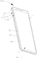
FIG. 1 illustrates a schematic perspective view of an electronic device, in accordance with an embodiment of the present disclosure; -
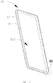
FIG. 2 illustrates a schematic perspective view of a frame assembly of the electronic device ofFIG. 1 ; -
FIG. 3 illustrates an enlarged schematic view of an area III of the frame assembly ofFIG. 2 , in accordance with another embodiment of the present disclosure; -
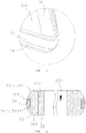
FIG. 4 illustrates a schematic cross-sectional view of the frame assembly ofFIG. 3 ; -
FIG. 5 illustrates an enlarged schematic view of an area III of the frame assembly ofFIG. 2 , in accordance with further another embodiment of the present disclosure; -
FIG. 6 illustrates a schematic cross-sectional view of the frame assembly ofFIG. 5 ; -
FIG. 7 illustrates a schematic cross-sectional view of the frame assembly ofFIG. 5 , in accordance with till another embodiment of the present disclosure; -
FIG. 8 illustrates a schematic cross-sectional view of the frame assembly ofFIG. 5 , in accordance with till another embodiment of the present disclosure; -
FIG. 9 illustrates a schematic cross-sectional view of the frame assembly ofFIG. 5 , in accordance with till another embodiment of the present disclosure; -
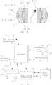
FIG. 10 illustrates a schematic view of a hardware environment of an electronic device, in accordance with an embodiment of the present disclosure. - As used herein, a "communication terminal", "electronic device" or simply a "terminal") includes, but is not limited to, a device that is configured to receive/transmit communication signals via a wire line connection, such as via a public-switched telephone network (PSTN), digital subscriber line (DSL), digital cable, a direct cable connection, and/or another data connection/network, and/or via a wireless interface with, for example, a cellular network, a wireless local area network (WLAN)1 a digital television network such as a DVB-H network, a satellite network, an AM/FM broadcast transmitter, and/or another communication terminal. A communication terminal or an electronic device that is configured to communicate over a wireless interface may be referred to as a "wireless communication terminal," a "wireless terminal" and/or a "mobile terminal." Examples of mobile terminals and electronic devices include, but are not limited to, a satellite or cellular radiotelephone; a Personal Communications System (PCS) terminal that may combine a cellular radiotelephone with data processing, facsimile and data communications capabilities; a PDA that can include a radiotelephone, pager, Internet/intranet access, Web browser, organizer, calendar and/or a global positioning system (GPS) receiver; and a conventional laptop and/or palmtop receiver or other appliance that includes a radiotelephone transceiver.
- In accordance with an aspect, in one embodiment of the present disclosure, a frame assembly for an electronic device is provided. The frame assembly includes a first frame and a second frame. The first frame defines a receiving space for accommodating electronic elements of the electronic device. The first frame includes an exterior surface departing from the receiving space. The second frame is coupled to the exterior surface of the first frame. The first frame is made of a glass material, and the second frame is made of a material different from the glass material of the first frame.
- In accordance with an aspect, in another embodiment of the present disclosure, a housing is provided. The housing includes a rear cover and a frame assembly coupled to the rear cover. The frame assembly includes a first frame and a second frame. The first frame defines a receiving space for accommodating electronic elements of the electronic device. The first frame includes an exterior surface departing from the receiving space. The second frame is coupled to the exterior surface of the first frame. The first frame is made of a glass material, and the second frame and the first frame are made of different materials.
- In accordance with an aspect, in further another embodiment of the present disclosure, an electronic device is provided. The electronic device includes a rear cover, a display module, and frame assembly. The rear cover and the display module are coupled to opposite sides of the frame assembly. The frame assembly includes a first frame and a second frame. The first frame defines a receiving space for accommodating electronic elements of the electronic device. The first frame includes an exterior surface departing from the receiving space. The second frame is coupled to the exterior surface of the
first frame 32. The first frame is a glass-made frame, and the second frame is a non-glass-made frame. - As illustrated in
FIG. 1 , anelectronic device 100 is provided, in accordance with an embodiment of the present disclosure. Theelectronic device 100 can be any device with communication function and storage function, such as: a tablet, a mobile phone, an e-reader, a remote control, a personal computer (PC), a notebook computer, car device, a network television, a wearable device smart, or other smart device with network capabilities. Theelectronic device 100 of the illustrated embodiment will be described by taking a mobile phone as an example. - The
electronic device 100 includes ahousing 12 and anelectronic component 10. Theelectronic component 10 includes adisplay module 14 and a plurality of electronic elements (not illustrated). Thedisplay module 14 is coupled to thehousing 12. The electronic elements are received in thehousing 12. - The
housing 12 is configured to support thedisplay module 14 and receive electronic elements of theelectronic device 100. In the embodiment illustrated inFIG. 1 , thehousing 12 includes afront cover 121, arear cover 123, and aframe assembly 30. Theframe assembly 30 is disposed between and coupled to thefront cover 121 and therear cover 123. Thedisplay module 14 coupled to one side of theframe assembly 30, and therear cover 123 is coupled to an opposite side of theframe assembly 30. - As illustrated in
FIG. 1 andFIG. 2 , in one embodiment, theframe assembly 30 may be a middle bezel assembly of theelectronic device 100. Theframe assembly 30 is substantially a rectangular frame and forms a frame of theelectronic device 100. In some embodiment, the frame of theelectronic device 100 may combine with the front surface by molding. In another embodiment, the frame may combine with the rear cover by molding. In still another embodiment, the frame may be an independent member and assembled to therear cover 123 and thefront cover 123. In the embodiment illustrated inFIG. 1 , theframe assembly 30 is assembled with therear cover 123 and thefront cover 121. - As illustrated in
FIG. 3 , theframe assembly 30 includes afirst frame 32 and asecond frame 34. Thefirst frame 32 defines a receivingspace 320 for accommodating the electronic elements of theelectronic device 100. Thesecond frame 34 is coupled to thefirst frame 32. Furthermore, thesecond frame 34 is coupled to an exterior surface of thefirst frame 32 departing away from the receivingspace 320. And thesecond frame 34 is extending around thefirst frame 32. Thefirst frame 32 is made of a glass material, and thesecond frame 34 is made of a material different from the glass material of thefirst frame 32. In other words, thesecond frame 34 is a non-glass frame, and thefirst frame 32 and the second frame are made of different material. By this way, the non-glass-madesecond frame 34 is disposed on an exterior surface of the glass-madefirst frame 32 to protect thefirst frame 32. And thesecond frame 34 can serve as a decoration and a bumper for theframe assembly 30 and theelectronic device 100. In some alternative embodiment, thesecond frame 34 may be a non-metal frame. - In some embodiments, the material of the
second frame 34 is selected from a group of metal, plastic, resin, or rubber, and any combination thereof. In some alternative embodiments, the material ofsecond frame 34 may be made of an elastic material, such as plastic, resin, and rubber, and any combination thereof. In one embodiment, a toughness of thesecond frame 34 is greater than a toughness of thefirst frame 32. - As illustrated in
FIG. 4 , in one embodiment, thefirst frame 32 includes aninterior surface 322 and an exterior surface 324. Theinterior surface 322 and the exterior surface 324 are disposed at two opposite sides of thefirst frame 32, and theinterior surface 322 faces the receivingspace 320. Thefirst frame 32 defines a mountinggroove 326 in the exterior surface 324. The mountinggroove 326 is configured to receive thesecond frame 34. The mountinggroove 326 extends along a periphery direction of thefirst frame 32, and thesecond frame 34 is engaged into the mountinggroove 326 and surrounds thefirst frame 32. - Furthermore, the mounting
groove 326 is located substantially at an intermediate position on the exterior surface 324 along a height direction of thefirst frame 32. So that thesecond frame 34 can be disposed at a peak of the exterior surface 324 when thesecond frame 34 is received in the mountinggroove 326. In one embodiment, an out surface of theframe assembly 30 is a curved surface, and thesecond frame 34 is located at a peak of the curved surface. That is, an out surface of thesecond frame 34 and theexterior surface 326 of the first frame 324 cooperatively form the out surface of theframe assembly 30. So that when theframe assembly 30 is dropped, an impact portion may firstly apply to thesecond frame 34. Therefore, a cushioning performance of thesecond frame 34 is effectively configured to protect theframe assembly 30 from damaged. It should be noted that the height direction of thefirst frame 32 described above should be considered as a direction that coincides with a thickness of theelectronic device 100. - Furthermore, the
second frame 34 includes an exposed surface 341 departing from the receivingspace 320. The exposed surface 341 is smoothly connected with the exterior surface 324 of thefirst frame 32. In some embodiments, the exterior surface 324 is a curved surface, and the exposed surface 341 is also a curved surface that continuous with the exterior surface 324. In the embodiment illustrated inFIG. 4 , in a cross-sectional view of theframe assembly 30 taken along the height direction thereof, a cross-sectional outer contour of the exterior surface 324 is presented as a first arc 3241, and a cross-sectional outer contour of the exposed surface 341 is presented as a second arc 3411 that continuous with the first arc 3241. The second arc 3411 is substantially smoothly coupled with the first arc 3241. So that theframe assembly 30 can have a smooth outer surface. In some alternative embodiments, the exposed surface 341 and the exterior surface 324 may be other structures except curved surfaces. For example, the exposed surface 341 and the exterior surface 324 may be planar surfaces or other curved surfaces (such as a concave curved surfaces, wave surfaces, etc.) - As illustrated in
FIG. 5 and FIG. 6 , in one embodiment, theframe assembly 30 further includes athird frame 36 coupled to theinterior surface 322 of thefirst frame 32. Thethird frame 36 is made of a metal to support thefirst frame 32. So that theframe assembly 30 can have a relatively high strength and toughness. In some alternative embodiments, the material of thethird frame 36 may be selected from the group of the iron, steel, stainless steel, copper, phosphor bronze, beryllium copper, nickel copper alloy, and magnesium aluminum alloy, etc., and any combination thereof. - Furthermore, in some embodiments, the
first frame 32 may be a transparent glass frame. Thethird frame 36 further includes adecorative pattern 360 formed on a surface thereof facing thefirst frame 32. So that a user can observe thedecorative pattern 360 through thefirst frame 32. Thedecorative pattern 360 of thethird frame 36 can be directly formed on thethird frame 36, and may be an etching pattern, a silk screen pattern, or a laser engraving pattern, or any combination of the above. - As illustrated in
FIG. 7 , in one embodiment, thefirst frame 32 further defines afirst mounting portion 3221 in theinterior surface 322 thereof, and thethird frame 36 further includes a second mountingportion 361 engaged with thefirst mounting portion 3221. Thesecond mounting portion 361 is embedded with thefirst mounting portion 3221. In the embodiment illustrated inFIG. 7 , thefirst mounting portion 3221 is a depression defined in the interior surface, and the second mountingportion 361 is a protrusion. The protrusion is cooperated with and received in the depression. Furthermore, thefirst mounting portion 3221 may be a groove extending in a circumferential direction of thefirst frame 32. In other embodiments, thefirst mounting portion 3221 may be a plurality of grooves discretely distributed on theinterior surface 322 of thefirst frame 32. In still other embodiments, thefirst mounting portion 3221 can be one or more protrusions, and the second mountingportion 361 can be one or more depressions. - In some embodiment, the
third frame 36 may be a closed loop or a non-closed loop structure. When thethird frame 36 is a closed loop, it may be an integrally formed closed annular frame, or may be a closed frame assembled together by a plurality of side frames. For example, thethird frame 36 may include a plurality of side frames, and the plurality of side frames are sequentially end to end to form a closed loop frame. The connection between the plurality of side frames may be an integrally molding connection or an assembled connection. When thethird frame 36 is a non-closed frame, it may define at least one opening. For example, thethird frame 36 may include a plurality of side frames coupled to theinterior surface 322, and at least two of the plurality of side frames are spaced apart from each other to form the opening such that thethird frame 36 is a non-closed frame. The opening may be an un-shielded slot that is filled with un-shielded material. - As illustrated in
FIG. 8 andFIG. 9 , in some embodiments, theframe assembly 30 further includes aninterlayer 38. Theinterlayer 38 is sandwiched between thefirst frame 32 and thethird frame 36. In the illustrated embodiments, theinterlayer 38 is an adhesive layer for bonding thethird frame 36 and thefirst frame 32. For example, theinterlayer 38 may be made of a bonding material such as glue or double-sided tape. In other embodiments, theinterlayer 38 may be a decorative layer. For example, theinterlayer 38 may be a decorative sheet disposed between thefirst frame 32 and thethird frame 36, such as a film sheet or other decorative material. In still other alternative embodiments, theinterlayer 38 can be a buffer layer for achieving and buffering between thefirst frame 32 and thethird frame 36. And theinterlayer 38 can be configured to absorb impact energy of theframe assembly 30 when dropped. Furthermore, theinterlayer 38 may be made of elastic material. For example, the material of theinterlayer 38 can be selected from a group of plastic, resin, and rubber, and any combination thereof. - Furthermore, in some embodiments, the
frame assembly 30 may define one or more through holes (not illustrated) therein. The through holes may be configured to accommodate one or more physical buttons of theelectronic device 100. The through hole can also be configured as a power entry, a data entry, a headphone hole, a speaker sound hole, a microphone sound entry, and the like of theelectronic device 100. The through hole may penetrate one or more of thefirst frame 32, thesecond frame 34, thethird frame 36, and theinterlayer 38. - In the
electronic device 100 provided in the present disclosure, by providing the non-glass-madesecond frame 34 coupled to the glass-madefirst frame 32, thesecond frame 34 can serve as a bumper of theframe assembly 30, and thefirst frame 32 is protected by thesecond frame 34. In addition, because thesecond frame 34 and thefirst frame 32 are made from different material, the non-glass-madesecond frame 34 can act as a decorative role. - As illustrated in
FIG. 10 , in the actual disclosure scenario, theelectronic device 100 can be used as a smart electronic device, such as a smart phone terminal, in which case theelectronic component 10 is usually further includes one or more (only one is illustrated)processors 102, amemory 104, a Radio Frequency (RF)module 106, anaudio circuit 110, a sensor, aninput module 118, and apower module 122. It will be understood by those skilled in the art that the structure illustrated inFIG. 10 is merely illustrative and does not limit the structure of theelectronic component 10. For example, theelectronic component 10 may include more or less components those illustrated inFIG. 10 , or have a different configuration that illustrated in FIG. - One of ordinary skill in the art will appreciate that all other components are peripherals relative to the
processor 102. Theprocessor 102 is coupled to the peripherals via a plurality ofperipheral interfaces 124. Theperipheral interface 124 can be implemented based on the following standards: Universal Asynchronous Receiver/Transmitter (UART), General Purpose Input Output (GPIO), Serial Peripheral Interface (SPI), Inter-Integrated Circuit (I2C), but not limited to the above standards. In some examples,peripheral interface 124 may only include a bus; in other examples,peripheral interface 124 may also include other components, such as one or more controllers, such as a display controller for connectingdisplay panel 143 or a memory controller configured to connect to the memory. In addition, these controllers can also be detached from theperipheral interface 124 and integrated into theprocessor 102 or within a corresponding peripheral. - The
memory 104 can be configured to store software programs and modules. Theprocessor 102 executes various functional disclosures and data processing by executing software programs and modules stored in thememory 104. Thememory 104 may include high speed random access memory and may also include non-volatile memory such as one or more magnetic storage devices, flash memory, or other non-volatile solid state memory. In some embodiments, thememory 104 may further include a memory remotely located relative toprocessor 102, which may be coupled to theelectronic component 10 ordisplay module 14 via a network. Examples of such networks may include, but are not limited to, the Internet, intranets, local area networks, mobile communication networks, and combinations thereof. - The
RF module 106 is configured to receive and transmit electromagnetic waves, and convert electromagnetic waves and electrical signals to communicate with a communication network or other device. TheRF module 106 can include various existing circuit components for performing the communication functions, such as an antenna, a radio frequency transceiver, a digital signal processor, an encryption/decryption chip, a Subscriber Identity Module (SIM) card, a memory, and the like. TheRF module 106 can communicate with various networks such as the Internet, an intranet, a wireless network, or communicate with other devices via a wireless network. The wireless network described above may include a cellular telephone network, a wireless local area network, or a metropolitan area network. The above wireless network can use various communication standards, protocols and technologies, including but not limited to Global System for Mobile Communication (GSM), Enhanced Data GSM Environment (EDGE), and wideband code. Wideband code division multiple access (W-CDMA), Code division access (CDMA), time division multiple access (TDMA), wireless fidelity (Wireless, Fidelity), Wi-Fi) (such as the Institute of Electrical and Electronics Engineers Standards IEEE 802.10A, IEEE 802.11b, IEEE 802.11g and / or IEEE 802.11n), Voice over internet protocol (VoIP), Worldwide Interoperability (Worldwide Interoperability) For Microwave Access, Wi-Max, other protocols for mail, instant messaging and short messages, and any other suitable communication protocols, even those that are not currently being developed. - The
audio circuit 110, thespeaker 101, thesound jack 103, and themicrophone 105 cooperatively provide an audio interface between a user and theelectronic component 10 or thedisplay module 14. In the illustrated embodiment, theaudio circuit 110 can receive a sound data from theprocessor 102, and theaudio circuit 110 can convert the sound data into an electrical signal, and transmit the electrical signal to thespeaker 101. Thespeaker 101 can convert the electrical signal into a sound wave that can be heard by a human ear. Theaudio circuit 110 can also receive electrical signals from themicrophone 105, and convert the electrical signals into sound data, and further transmit the sound data to theprocessor 102 for further processing. The audio data may be obtained frommemory 104 or theRF module 106. Additionally, audio data may also be stored inmemory 104 or transmitted by theRF module 106. - Sensors are disposed in the
electronic component 10 or in thedisplay module 14. Examples of the sensors can include, but are not limited to, light sensors, operational sensors, pressure sensors, gravity acceleration sensors, and other sensors. - In this embodiment, the
input module 118 can include atouch screen 109 disposed on thedisplay module 14. Thetouch screen 109 can collect touch operations on or near the touch screen 109 (such as a user using a finger, a stylus, etc., or any suitable object or accessory operates on or adjacent to the touch screen 109), and drive a corresponding connection device according to a predetermined program. Alternatively,touch screen 109 may include a touch detector and a touch controller. Wherein, the touch detector can detect the touch orientation of the user, and detect a signal brought by the touch operation, and transmits a touch signal to the touch controller. The touch controller can receive the touch signal from the touch detector, and convert the touch signal into touch coordinates, and then transmit the touch coordinates to theprocessor 102, and can receive a command generated by theprocessor 102 and execute it. In addition, the touch detection function of thetouch screen 109 can be implemented by various types such as resistive, capacitive, infrared, and surface acoustic waves. In addition to touchingdisplay 109, in other variant embodiments,input module 118 may also include other input devices, such asbutton 107. Thebutton 107 may include, for example, a character button for inputting a character, and a control button for triggering a control function. Examples of control buttons include a "return to home screen" button, a power on/off button, and the like. - The
display module 14 is configured to display information input by the user, information provided to the user, and various graphical user interfaces of theelectronic component 10, which can be composed of graphics, text, icons, numbers, videos, and any combination thereof. In one example, thetouch screen 109 can be disposed on thedisplay panel 143 to be integrated with thedisplay panel 143. - The
power module 122 is configured to provide power to theprocessor 102 and other components. In the illustrated embodiment, thepower module 122 may include a power management system, one or more power sources (such as a battery or an alternating current), a charging circuit, a power failure detecting circuit, an inverter, a power status indicator, and any other with theelectronic component 10 or a components related to the generation, management, and distribution of power within the display module14. - The
electronic device 100 can also include a locator for determining the actual location at which theelectronic device 100 is located. In this embodiment, the locator applies a location service to implement the positioning of theelectronic device 100. The positioning service should be understood as a technology or service of the location of the object being located, which acquire the location information (such as latitude and longitude coordinates) of theelectronic device 100 by using a specific positioning technology, and marking the electronic map.
Claims (13)
- A frame assembly (30) for an electronic device, comprising:a first frame (32) defining a receiving space (320) for accommodating electronic elements of the electronic device (100), the first frame (32) comprising an exterior surface (324) departing from the receiving space (320); anda second frame (34) coupled to the exterior surface (324) of the first frame (32); whereinthe first frame (32) defines a mounting groove (326) in the exterior surface(324); the mounting groove (326) extends along a periphery direction of the first frame (32); the second frame (34) is engaged into the mounting groove (326) and surrounds the first frame (32); the first frame (32) is made of a glass material, and the second frame (34) is made of a material different from the glass material of the first frame (32); the second frame (34) comprises an exposed surface (341) departing from the receiving space (320); the exposed surface (341) is smoothly connected with the exterior surface (324) of the first frame (32); an outer surface of the frame assembly (30) is formed by the exposed surface (341) and the exterior surface (324), and the outer surface is departing from the receiving space (320).
- The frame assembly (30) as claimed in claim 1, wherein the material of the second frame (34) is selected from a group of metal, plastic, resin, rubber, and any combination thereof.
- The frame assembly (30) as claimed in any one of claims 1 to 2, wherein the exterior surface (324) is a curved surface, and the exposed surface (341) is a curved surface; the exposed surface (341) is continuous with the exterior surface (324).
- The frame assembly (30) as claimed in any one of claims 1 to 3, wherein the first frame (32) further comprises an interior surface (322) facing the receiving space (320), the frame assembly (30) further comprises a third frame (36), and the third frame (36) is coupled to the interior surface (322) of the first frame (32).
- The frame assembly (30) as claimed in claim 4, wherein the third frame (36) is made of a material selected from a group of iron, steel, stainless steel, copper, phosphor bronze, copper, beryllium copper, nickel copper alloy, magnesium alloy, and any combination thereof.
- The frame assembly (30) as claimed in any one of claims 4 to 5 , wherein the first frame (32) is transparent, and the third frame (36) has a surface facing the first frame (32), and a decorative pattern (360) is formed on the surface facing the first frame (32).
- The frame assembly (30) as claimed in any one of claims 4 to 6, wherein the first frame (32) further defines a first mounting portion (3221) in the interior surface (322), and the third frame (36) further comprises a second mounting portion (361); the second mounting portion (361) is engaged with the first mounting portion (3221).
- The frame assembly (30) as claimed in claim 7, wherein the first mounting portion (3221) is a depression defined in the interior surface (322), the second mounting portion (361) is a protrusion cooperated with and received in the depression.
- The frame assembly (30) as claimed in any one of claims 4 to 8 , wherein the third frame (36) is a closed loop frame or a non-closed loop frame.
- The frame assembly (30) as claimed in any one of claims 4 to 8, wherein the frame assembly (30) further comprises an interlayer (38); the interlayer (38) is sandwiched between the third frame (36) and the first frame (32).
- A housing (12) for an electronic device (100), comprising:a rear cover (123), andthe frame assembly (30) of any one of claims 1 to 10.
- The housing (12) as claimed in claim 11, wherein the first frame (32) further comprises an interior surface (322) facing the receiving space (320), and the frame assembly (30) further comprises a third frame (36); the third frame (36) is coupled to the interior surface (322).
- An electronic device (100), comprising:a rear cover (123);a display module (14); andthe frame assembly (30) of any one of claims 1 to 10.
Applications Claiming Priority (2)
| Application Number | Priority Date | Filing Date | Title |
|---|---|---|---|
| CN201810075034.5A CN110086897B (en) | 2018-01-25 | 2018-01-25 | Mobile terminal and shell and middle frame structure thereof |
| CN201820128315.8U CN207802039U (en) | 2018-01-25 | 2018-01-25 | Mobile terminal and its shell and middle frame structure |
Publications (2)
| Publication Number | Publication Date |
|---|---|
| EP3518510A1 EP3518510A1 (en) | 2019-07-31 |
| EP3518510B1 true EP3518510B1 (en) | 2021-01-06 |
Family
ID=64564575
Family Applications (1)
| Application Number | Title | Priority Date | Filing Date |
|---|---|---|---|
| EP18209179.3A Not-in-force EP3518510B1 (en) | 2018-01-25 | 2018-11-29 | Frame assembly, housing and electronic device having the same |
Country Status (6)
| Country | Link |
|---|---|
| US (1) | US20190230203A1 (en) |
| EP (1) | EP3518510B1 (en) |
| DK (1) | DK3518510T3 (en) |
| ES (1) | ES2861304T3 (en) |
| PT (1) | PT3518510T (en) |
| WO (1) | WO2019144718A1 (en) |
Families Citing this family (2)
| Publication number | Priority date | Publication date | Assignee | Title |
|---|---|---|---|---|
| US12136940B2 (en) * | 2019-01-08 | 2024-11-05 | Imtechnology.Co., Ltd | Mobile device case and coating method thereof |
| EP4271148B1 (en) | 2021-01-29 | 2025-11-26 | Samsung Electronics Co., Ltd. | Electronic device comprising housing assembly structure |
Family Cites Families (23)
| Publication number | Priority date | Publication date | Assignee | Title |
|---|---|---|---|---|
| US6639577B2 (en) * | 1998-03-04 | 2003-10-28 | Gemstar-Tv Guide International, Inc. | Portable information display device with ergonomic bezel |
| US8306574B2 (en) * | 2003-10-29 | 2012-11-06 | Robert Warner | Method and system for an adaptive wireless communication system optimized for economic benefit |
| US7382607B2 (en) * | 2006-02-16 | 2008-06-03 | Palm, Inc. | Housing for a portable computing device |
| JP4866154B2 (en) * | 2006-06-05 | 2012-02-01 | 株式会社 日立ディスプレイズ | Liquid crystal display |
| JP5106275B2 (en) * | 2008-06-30 | 2012-12-26 | 株式会社東芝 | Wireless communication apparatus and wireless communication method |
| US20100059649A1 (en) * | 2008-09-06 | 2010-03-11 | Pierce Alfred Buxton | Integrated Frame/Stand for Portable Electronic Devices |
| US8331303B2 (en) * | 2010-02-26 | 2012-12-11 | Hewlett-Packard Development Company, L.P. | Adaptive wireless network |
| US8411608B2 (en) * | 2010-02-26 | 2013-04-02 | Microsoft Corporation | Efficient and reliable multicast over a Wi-Fi network |
| CN102404423A (en) * | 2010-09-14 | 2012-04-04 | 陈柄华 | Fixing structure for mobile phone touch screen |
| US8464417B2 (en) * | 2011-02-09 | 2013-06-18 | Apple Inc. | Method for cover glass removal |
| CN104317360B (en) * | 2011-06-13 | 2018-09-28 | 树蛙开发公司 | Shell for protecting tablet computer |
| US8861198B1 (en) * | 2012-03-27 | 2014-10-14 | Amazon Technologies, Inc. | Device frame having mechanically bonded metal and plastic |
| GB201214120D0 (en) * | 2012-08-07 | 2012-09-19 | Yota Devices Ipr Ltd | Yota 070812 |
| US20140028162A1 (en) * | 2012-07-26 | 2014-01-30 | Michelle Lynn Carlson | Case for portable electronic device |
| CN203608244U (en) * | 2013-12-24 | 2014-05-21 | 罗海城 | Digital equipment protection frame |
| WO2015097938A1 (en) * | 2013-12-25 | 2015-07-02 | パナソニックIpマネジメント株式会社 | Electronic device |
| US20150281415A1 (en) * | 2014-03-28 | 2015-10-01 | Shu-Wei Lin | Metal protector frame assembly for mobile phone |
| US9750022B2 (en) * | 2014-08-07 | 2017-08-29 | Cisco Technology, Inc. | High-density wireless band steering based on wireless device address |
| CN105792560B (en) * | 2014-12-24 | 2020-01-31 | 深圳富泰宏精密工业有限公司 | Shell, electronic device applying shell and manufacturing method of electronic device |
| CN105007346A (en) * | 2015-07-27 | 2015-10-28 | 东莞市瑞必达科技股份有限公司 | Stereoscopic glass cover-plate structure and manufacturing method thereof |
| US20170048728A1 (en) * | 2015-08-10 | 2017-02-16 | Network Performance Research Group Llc | Method and apparatus for directed adaptive control of access point-to-client interaction in wireless networks |
| KR102448304B1 (en) * | 2016-02-04 | 2022-09-28 | 삼성전자 주식회사 | Electronic device comprising a metal housing |
| CN207802039U (en) * | 2018-01-25 | 2018-08-31 | 广东欧珀移动通信有限公司 | Mobile terminal and its shell and middle frame structure |
-
2018
- 2018-11-27 US US16/202,017 patent/US20190230203A1/en not_active Abandoned
- 2018-11-29 PT PT182091793T patent/PT3518510T/en unknown
- 2018-11-29 ES ES18209179T patent/ES2861304T3/en active Active
- 2018-11-29 EP EP18209179.3A patent/EP3518510B1/en not_active Not-in-force
- 2018-11-29 DK DK18209179.3T patent/DK3518510T3/en active
- 2018-12-12 WO PCT/CN2018/120718 patent/WO2019144718A1/en not_active Ceased
Non-Patent Citations (1)
| Title |
|---|
| None * |
Also Published As
| Publication number | Publication date |
|---|---|
| WO2019144718A1 (en) | 2019-08-01 |
| ES2861304T3 (en) | 2021-10-06 |
| US20190230203A1 (en) | 2019-07-25 |
| PT3518510T (en) | 2021-02-16 |
| DK3518510T3 (en) | 2021-03-01 |
| EP3518510A1 (en) | 2019-07-31 |
Similar Documents
| Publication | Publication Date | Title |
|---|---|---|
| US10819889B2 (en) | Camera device and mobile terminal using same | |
| EP3484131B1 (en) | Camera device of a mobile terminal | |
| CN107896261A (en) | Mobile terminal and display module thereof | |
| US20210136189A1 (en) | Electronic device and front shell thereof | |
| CN207802039U (en) | Mobile terminal and its shell and middle frame structure | |
| CN208445606U (en) | Housing unit and electronic equipment | |
| CN207802040U (en) | Mobile terminal and its shell and middle frame structure | |
| EP3518510A1 (en) | Frame assembly, housing and electronic device having the same | |
| CN111314531B (en) | Electronic equipment and shell assembly thereof | |
| CN108811285B (en) | Electronic equipment | |
| CN111447352B (en) | Brackets, camera components and terminal equipment | |
| EP3547443B1 (en) | Electronic device and control method thereof | |
| CN110086896A (en) | Mobile terminal and its shell and middle frame structure | |
| WO2019072121A1 (en) | Electronic device and intermediate frame structure thereof | |
| CN110086897B (en) | Mobile terminal and shell and middle frame structure thereof | |
| CN207518650U (en) | Mobile terminal | |
| CN109005257B (en) | Electronic device | |
| CN109005258B (en) | Electronic equipment | |
| CN207625612U (en) | Mobile terminal and its earphone seat installation structure | |
| CN108882093B (en) | Electronic device | |
| HK40009396A (en) | Mobile terminal and shell and middle frame structure thereof | |
| CN108228507B (en) | Mobile terminal and housing assembly thereof | |
| HK40003341B (en) | Camera device of a mobile terminal | |
| HK40003341A (en) | Camera device of a mobile terminal | |
| HK40006151A (en) | Camera device, bracket and mobile terminal using same |
Legal Events
| Date | Code | Title | Description |
|---|---|---|---|
| PUAI | Public reference made under article 153(3) epc to a published international application that has entered the european phase |
Free format text: ORIGINAL CODE: 0009012 |
|
| STAA | Information on the status of an ep patent application or granted ep patent |
Free format text: STATUS: THE APPLICATION HAS BEEN PUBLISHED |
|
| AK | Designated contracting states |
Kind code of ref document: A1 Designated state(s): AL AT BE BG CH CY CZ DE DK EE ES FI FR GB GR HR HU IE IS IT LI LT LU LV MC MK MT NL NO PL PT RO RS SE SI SK SM TR |
|
| AX | Request for extension of the european patent |
Extension state: BA ME |
|
| RAP1 | Party data changed (applicant data changed or rights of an application transferred) |
Owner name: GUANGDONG OPPO MOBILE TELECOMMUNICATIONS CORP., LT |
|
| STAA | Information on the status of an ep patent application or granted ep patent |
Free format text: STATUS: REQUEST FOR EXAMINATION WAS MADE |
|
| 17P | Request for examination filed |
Effective date: 20200109 |
|
| RBV | Designated contracting states (corrected) |
Designated state(s): AL AT BE BG CH CY CZ DE DK EE ES FI FR GB GR HR HU IE IS IT LI LT LU LV MC MK MT NL NO PL PT RO RS SE SI SK SM TR |
|
| GRAP | Despatch of communication of intention to grant a patent |
Free format text: ORIGINAL CODE: EPIDOSNIGR1 |
|
| STAA | Information on the status of an ep patent application or granted ep patent |
Free format text: STATUS: GRANT OF PATENT IS INTENDED |
|
| INTG | Intention to grant announced |
Effective date: 20200827 |
|
| GRAS | Grant fee paid |
Free format text: ORIGINAL CODE: EPIDOSNIGR3 |
|
| GRAA | (expected) grant |
Free format text: ORIGINAL CODE: 0009210 |
|
| STAA | Information on the status of an ep patent application or granted ep patent |
Free format text: STATUS: THE PATENT HAS BEEN GRANTED |
|
| AK | Designated contracting states |
Kind code of ref document: B1 Designated state(s): AL AT BE BG CH CY CZ DE DK EE ES FI FR GB GR HR HU IE IS IT LI LT LU LV MC MK MT NL NO PL PT RO RS SE SI SK SM TR |
|
| REG | Reference to a national code |
Ref country code: GB Ref legal event code: FG4D |
|
| REG | Reference to a national code |
Ref country code: AT Ref legal event code: REF Ref document number: 1353600 Country of ref document: AT Kind code of ref document: T Effective date: 20210115 Ref country code: CH Ref legal event code: EP |
|
| REG | Reference to a national code |
Ref country code: DE Ref legal event code: R096 Ref document number: 602018011590 Country of ref document: DE |
|
| REG | Reference to a national code |
Ref country code: IE Ref legal event code: FG4D |
|
| REG | Reference to a national code |
Ref country code: PT Ref legal event code: SC4A Ref document number: 3518510 Country of ref document: PT Date of ref document: 20210216 Kind code of ref document: T Free format text: AVAILABILITY OF NATIONAL TRANSLATION Effective date: 20210210 |
|
| REG | Reference to a national code |
Ref country code: DK Ref legal event code: T3 Effective date: 20210225 Ref country code: FI Ref legal event code: FGE |
|
| REG | Reference to a national code |
Ref country code: NL Ref legal event code: FP |
|
| REG | Reference to a national code |
Ref country code: SE Ref legal event code: TRGR |
|
| REG | Reference to a national code |
Ref country code: NO Ref legal event code: T2 Effective date: 20210106 |
|
| REG | Reference to a national code |
Ref country code: LT Ref legal event code: MG9D |
|
| PG25 | Lapsed in a contracting state [announced via postgrant information from national office to epo] |
Ref country code: LT Free format text: LAPSE BECAUSE OF FAILURE TO SUBMIT A TRANSLATION OF THE DESCRIPTION OR TO PAY THE FEE WITHIN THE PRESCRIBED TIME-LIMIT Effective date: 20210106 Ref country code: BG Free format text: LAPSE BECAUSE OF FAILURE TO SUBMIT A TRANSLATION OF THE DESCRIPTION OR TO PAY THE FEE WITHIN THE PRESCRIBED TIME-LIMIT Effective date: 20210406 Ref country code: GR Free format text: LAPSE BECAUSE OF FAILURE TO SUBMIT A TRANSLATION OF THE DESCRIPTION OR TO PAY THE FEE WITHIN THE PRESCRIBED TIME-LIMIT Effective date: 20210407 Ref country code: HR Free format text: LAPSE BECAUSE OF FAILURE TO SUBMIT A TRANSLATION OF THE DESCRIPTION OR TO PAY THE FEE WITHIN THE PRESCRIBED TIME-LIMIT Effective date: 20210106 |
|
| PG25 | Lapsed in a contracting state [announced via postgrant information from national office to epo] |
Ref country code: RS Free format text: LAPSE BECAUSE OF FAILURE TO SUBMIT A TRANSLATION OF THE DESCRIPTION OR TO PAY THE FEE WITHIN THE PRESCRIBED TIME-LIMIT Effective date: 20210106 Ref country code: LV Free format text: LAPSE BECAUSE OF FAILURE TO SUBMIT A TRANSLATION OF THE DESCRIPTION OR TO PAY THE FEE WITHIN THE PRESCRIBED TIME-LIMIT Effective date: 20210106 Ref country code: PL Free format text: LAPSE BECAUSE OF FAILURE TO SUBMIT A TRANSLATION OF THE DESCRIPTION OR TO PAY THE FEE WITHIN THE PRESCRIBED TIME-LIMIT Effective date: 20210106 |
|
| PG25 | Lapsed in a contracting state [announced via postgrant information from national office to epo] |
Ref country code: IS Free format text: LAPSE BECAUSE OF FAILURE TO SUBMIT A TRANSLATION OF THE DESCRIPTION OR TO PAY THE FEE WITHIN THE PRESCRIBED TIME-LIMIT Effective date: 20210506 |
|
| REG | Reference to a national code |
Ref country code: ES Ref legal event code: FG2A Ref document number: 2861304 Country of ref document: ES Kind code of ref document: T3 Effective date: 20211006 |
|
| REG | Reference to a national code |
Ref country code: DE Ref legal event code: R097 Ref document number: 602018011590 Country of ref document: DE |
|
| PG25 | Lapsed in a contracting state [announced via postgrant information from national office to epo] |
Ref country code: CZ Free format text: LAPSE BECAUSE OF FAILURE TO SUBMIT A TRANSLATION OF THE DESCRIPTION OR TO PAY THE FEE WITHIN THE PRESCRIBED TIME-LIMIT Effective date: 20210106 Ref country code: EE Free format text: LAPSE BECAUSE OF FAILURE TO SUBMIT A TRANSLATION OF THE DESCRIPTION OR TO PAY THE FEE WITHIN THE PRESCRIBED TIME-LIMIT Effective date: 20210106 Ref country code: SM Free format text: LAPSE BECAUSE OF FAILURE TO SUBMIT A TRANSLATION OF THE DESCRIPTION OR TO PAY THE FEE WITHIN THE PRESCRIBED TIME-LIMIT Effective date: 20210106 |
|
| PLBE | No opposition filed within time limit |
Free format text: ORIGINAL CODE: 0009261 |
|
| STAA | Information on the status of an ep patent application or granted ep patent |
Free format text: STATUS: NO OPPOSITION FILED WITHIN TIME LIMIT |
|
| PG25 | Lapsed in a contracting state [announced via postgrant information from national office to epo] |
Ref country code: SK Free format text: LAPSE BECAUSE OF FAILURE TO SUBMIT A TRANSLATION OF THE DESCRIPTION OR TO PAY THE FEE WITHIN THE PRESCRIBED TIME-LIMIT Effective date: 20210106 Ref country code: RO Free format text: LAPSE BECAUSE OF FAILURE TO SUBMIT A TRANSLATION OF THE DESCRIPTION OR TO PAY THE FEE WITHIN THE PRESCRIBED TIME-LIMIT Effective date: 20210106 |
|
| 26N | No opposition filed |
Effective date: 20211007 |
|
| PG25 | Lapsed in a contracting state [announced via postgrant information from national office to epo] |
Ref country code: AL Free format text: LAPSE BECAUSE OF FAILURE TO SUBMIT A TRANSLATION OF THE DESCRIPTION OR TO PAY THE FEE WITHIN THE PRESCRIBED TIME-LIMIT Effective date: 20210106 |
|
| PG25 | Lapsed in a contracting state [announced via postgrant information from national office to epo] |
Ref country code: SI Free format text: LAPSE BECAUSE OF FAILURE TO SUBMIT A TRANSLATION OF THE DESCRIPTION OR TO PAY THE FEE WITHIN THE PRESCRIBED TIME-LIMIT Effective date: 20210106 |
|
| PG25 | Lapsed in a contracting state [announced via postgrant information from national office to epo] |
Ref country code: IS Free format text: LAPSE BECAUSE OF FAILURE TO SUBMIT A TRANSLATION OF THE DESCRIPTION OR TO PAY THE FEE WITHIN THE PRESCRIBED TIME-LIMIT Effective date: 20210506 |
|
| PG25 | Lapsed in a contracting state [announced via postgrant information from national office to epo] |
Ref country code: MC Free format text: LAPSE BECAUSE OF FAILURE TO SUBMIT A TRANSLATION OF THE DESCRIPTION OR TO PAY THE FEE WITHIN THE PRESCRIBED TIME-LIMIT Effective date: 20210106 |
|
| REG | Reference to a national code |
Ref country code: CH Ref legal event code: PL |
|
| PG25 | Lapsed in a contracting state [announced via postgrant information from national office to epo] |
Ref country code: LU Free format text: LAPSE BECAUSE OF NON-PAYMENT OF DUE FEES Effective date: 20211129 Ref country code: BE Free format text: LAPSE BECAUSE OF NON-PAYMENT OF DUE FEES Effective date: 20211130 |
|
| REG | Reference to a national code |
Ref country code: BE Ref legal event code: MM Effective date: 20211130 |
|
| PG25 | Lapsed in a contracting state [announced via postgrant information from national office to epo] |
Ref country code: IE Free format text: LAPSE BECAUSE OF NON-PAYMENT OF DUE FEES Effective date: 20211129 |
|
| PGFP | Annual fee paid to national office [announced via postgrant information from national office to epo] |
Ref country code: SE Payment date: 20221122 Year of fee payment: 5 Ref country code: PT Payment date: 20221121 Year of fee payment: 5 Ref country code: NO Payment date: 20221121 Year of fee payment: 5 Ref country code: NL Payment date: 20221118 Year of fee payment: 5 Ref country code: IT Payment date: 20221130 Year of fee payment: 5 Ref country code: GB Payment date: 20221123 Year of fee payment: 5 Ref country code: FR Payment date: 20221118 Year of fee payment: 5 Ref country code: FI Payment date: 20221117 Year of fee payment: 5 Ref country code: ES Payment date: 20221216 Year of fee payment: 5 Ref country code: DK Payment date: 20221122 Year of fee payment: 5 Ref country code: DE Payment date: 20220621 Year of fee payment: 5 |
|
| P01 | Opt-out of the competence of the unified patent court (upc) registered |
Effective date: 20230412 |
|
| PG25 | Lapsed in a contracting state [announced via postgrant information from national office to epo] |
Ref country code: CY Free format text: LAPSE BECAUSE OF FAILURE TO SUBMIT A TRANSLATION OF THE DESCRIPTION OR TO PAY THE FEE WITHIN THE PRESCRIBED TIME-LIMIT Effective date: 20210106 |
|
| PG25 | Lapsed in a contracting state [announced via postgrant information from national office to epo] |
Ref country code: LI Free format text: LAPSE BECAUSE OF NON-PAYMENT OF DUE FEES Effective date: 20220701 Ref country code: HU Free format text: LAPSE BECAUSE OF FAILURE TO SUBMIT A TRANSLATION OF THE DESCRIPTION OR TO PAY THE FEE WITHIN THE PRESCRIBED TIME-LIMIT; INVALID AB INITIO Effective date: 20181129 Ref country code: CH Free format text: LAPSE BECAUSE OF NON-PAYMENT OF DUE FEES Effective date: 20220701 |
|
| PG25 | Lapsed in a contracting state [announced via postgrant information from national office to epo] |
Ref country code: MK Free format text: LAPSE BECAUSE OF FAILURE TO SUBMIT A TRANSLATION OF THE DESCRIPTION OR TO PAY THE FEE WITHIN THE PRESCRIBED TIME-LIMIT Effective date: 20210106 |
|
| REG | Reference to a national code |
Ref country code: DE Ref legal event code: R119 Ref document number: 602018011590 Country of ref document: DE |
|
| REG | Reference to a national code |
Ref country code: DK Ref legal event code: EBP Effective date: 20231130 |
|
| PG25 | Lapsed in a contracting state [announced via postgrant information from national office to epo] |
Ref country code: TR Free format text: LAPSE BECAUSE OF FAILURE TO SUBMIT A TRANSLATION OF THE DESCRIPTION OR TO PAY THE FEE WITHIN THE PRESCRIBED TIME-LIMIT Effective date: 20210106 |
|
| REG | Reference to a national code |
Ref country code: SE Ref legal event code: EUG |
|
| REG | Reference to a national code |
Ref country code: NL Ref legal event code: MM Effective date: 20231201 |
|
| GBPC | Gb: european patent ceased through non-payment of renewal fee |
Effective date: 20231129 |
|
| PG25 | Lapsed in a contracting state [announced via postgrant information from national office to epo] |
Ref country code: NO Free format text: LAPSE BECAUSE OF NON-PAYMENT OF DUE FEES Effective date: 20231130 Ref country code: FI Free format text: LAPSE BECAUSE OF NON-PAYMENT OF DUE FEES Effective date: 20231129 |
|
| PG25 | Lapsed in a contracting state [announced via postgrant information from national office to epo] |
Ref country code: PT Free format text: LAPSE BECAUSE OF NON-PAYMENT OF DUE FEES Effective date: 20240529 |
|
| PG25 | Lapsed in a contracting state [announced via postgrant information from national office to epo] |
Ref country code: SE Free format text: LAPSE BECAUSE OF NON-PAYMENT OF DUE FEES Effective date: 20231130 Ref country code: PT Free format text: LAPSE BECAUSE OF NON-PAYMENT OF DUE FEES Effective date: 20240529 |
|
| PG25 | Lapsed in a contracting state [announced via postgrant information from national office to epo] |
Ref country code: NL Free format text: LAPSE BECAUSE OF NON-PAYMENT OF DUE FEES Effective date: 20231201 |
|
| PG25 | Lapsed in a contracting state [announced via postgrant information from national office to epo] |
Ref country code: NL Free format text: LAPSE BECAUSE OF NON-PAYMENT OF DUE FEES Effective date: 20231201 Ref country code: MT Free format text: LAPSE BECAUSE OF FAILURE TO SUBMIT A TRANSLATION OF THE DESCRIPTION OR TO PAY THE FEE WITHIN THE PRESCRIBED TIME-LIMIT Effective date: 20210106 |
|
| PG25 | Lapsed in a contracting state [announced via postgrant information from national office to epo] |
Ref country code: DE Free format text: LAPSE BECAUSE OF NON-PAYMENT OF DUE FEES Effective date: 20240601 |
|
| PG25 | Lapsed in a contracting state [announced via postgrant information from national office to epo] |
Ref country code: DK Free format text: LAPSE BECAUSE OF NON-PAYMENT OF DUE FEES Effective date: 20231130 |
|
| PG25 | Lapsed in a contracting state [announced via postgrant information from national office to epo] |
Ref country code: GB Free format text: LAPSE BECAUSE OF NON-PAYMENT OF DUE FEES Effective date: 20231129 |
|
| PG25 | Lapsed in a contracting state [announced via postgrant information from national office to epo] |
Ref country code: FR Free format text: LAPSE BECAUSE OF NON-PAYMENT OF DUE FEES Effective date: 20231130 |
|
| PG25 | Lapsed in a contracting state [announced via postgrant information from national office to epo] |
Ref country code: GB Free format text: LAPSE BECAUSE OF NON-PAYMENT OF DUE FEES Effective date: 20231129 Ref country code: FR Free format text: LAPSE BECAUSE OF NON-PAYMENT OF DUE FEES Effective date: 20231130 Ref country code: DK Free format text: LAPSE BECAUSE OF NON-PAYMENT OF DUE FEES Effective date: 20231130 Ref country code: DE Free format text: LAPSE BECAUSE OF NON-PAYMENT OF DUE FEES Effective date: 20240601 |
|
| PG25 | Lapsed in a contracting state [announced via postgrant information from national office to epo] |
Ref country code: IT Free format text: LAPSE BECAUSE OF NON-PAYMENT OF DUE FEES Effective date: 20231129 |
|
| PG25 | Lapsed in a contracting state [announced via postgrant information from national office to epo] |
Ref country code: IT Free format text: LAPSE BECAUSE OF NON-PAYMENT OF DUE FEES Effective date: 20231129 |
|
| REG | Reference to a national code |
Ref country code: ES Ref legal event code: FD2A Effective date: 20250102 |
|
| REG | Reference to a national code |
Ref country code: AT Ref legal event code: MM01 Ref document number: 1353600 Country of ref document: AT Kind code of ref document: T Effective date: 20231129 |
|
| PG25 | Lapsed in a contracting state [announced via postgrant information from national office to epo] |
Ref country code: AT Free format text: LAPSE BECAUSE OF NON-PAYMENT OF DUE FEES Effective date: 20231129 |
|
| PG25 | Lapsed in a contracting state [announced via postgrant information from national office to epo] |
Ref country code: ES Free format text: LAPSE BECAUSE OF NON-PAYMENT OF DUE FEES Effective date: 20231130 |
|
| PG25 | Lapsed in a contracting state [announced via postgrant information from national office to epo] |
Ref country code: ES Free format text: LAPSE BECAUSE OF NON-PAYMENT OF DUE FEES Effective date: 20231130 Ref country code: AT Free format text: LAPSE BECAUSE OF NON-PAYMENT OF DUE FEES Effective date: 20231129 |
|
| PGFP | Annual fee paid to national office [announced via postgrant information from national office to epo] |
Ref country code: AT Payment date: 20260410 Year of fee payment: 5 |