EP3518424A1 - Analog-to-digital converter capable of generate digital output signal having different bits - Google Patents
Analog-to-digital converter capable of generate digital output signal having different bits Download PDFInfo
- Publication number
- EP3518424A1 EP3518424A1 EP18211372.0A EP18211372A EP3518424A1 EP 3518424 A1 EP3518424 A1 EP 3518424A1 EP 18211372 A EP18211372 A EP 18211372A EP 3518424 A1 EP3518424 A1 EP 3518424A1
- Authority
- EP
- European Patent Office
- Prior art keywords
- adc
- signal
- generate
- digital output
- low power
- Prior art date
- Legal status (The legal status is an assumption and is not a legal conclusion. Google has not performed a legal analysis and makes no representation as to the accuracy of the status listed.)
- Ceased
Links
Images





Classifications
-
- H—ELECTRICITY
- H03—ELECTRONIC CIRCUITRY
- H03M—CODING; DECODING; CODE CONVERSION IN GENERAL
- H03M3/00—Conversion of analogue values to or from differential modulation
- H03M3/30—Delta-sigma modulation
- H03M3/32—Delta-sigma modulation with special provisions or arrangements for power saving, e.g. by allowing a sleep mode, using lower supply voltage for downstream stages, using multiple clock domains, by selectively turning on stages when needed
-
- H—ELECTRICITY
- H03—ELECTRONIC CIRCUITRY
- H03M—CODING; DECODING; CODE CONVERSION IN GENERAL
- H03M1/00—Analogue/digital conversion; Digital/analogue conversion
- H03M1/004—Reconfigurable analogue/digital or digital/analogue converters
- H03M1/007—Reconfigurable analogue/digital or digital/analogue converters among different resolutions
-
- H—ELECTRICITY
- H03—ELECTRONIC CIRCUITRY
- H03M—CODING; DECODING; CODE CONVERSION IN GENERAL
- H03M1/00—Analogue/digital conversion; Digital/analogue conversion
- H03M1/12—Analogue/digital converters
- H03M1/34—Analogue value compared with reference values
-
- H—ELECTRICITY
- H03—ELECTRONIC CIRCUITRY
- H03M—CODING; DECODING; CODE CONVERSION IN GENERAL
- H03M3/00—Conversion of analogue values to or from differential modulation
- H03M3/30—Delta-sigma modulation
- H03M3/39—Structural details of delta-sigma modulators, e.g. incremental delta-sigma modulators
- H03M3/412—Structural details of delta-sigma modulators, e.g. incremental delta-sigma modulators characterised by the number of quantisers and their type and resolution
- H03M3/422—Structural details of delta-sigma modulators, e.g. incremental delta-sigma modulators characterised by the number of quantisers and their type and resolution having one quantiser only
- H03M3/424—Structural details of delta-sigma modulators, e.g. incremental delta-sigma modulators characterised by the number of quantisers and their type and resolution having one quantiser only the quantiser being a multiple bit one
- H03M3/426—Structural details of delta-sigma modulators, e.g. incremental delta-sigma modulators characterised by the number of quantisers and their type and resolution having one quantiser only the quantiser being a multiple bit one the quantiser being a successive approximation type analogue/digital converter
-
- H—ELECTRICITY
- H03—ELECTRONIC CIRCUITRY
- H03M—CODING; DECODING; CODE CONVERSION IN GENERAL
- H03M3/00—Conversion of analogue values to or from differential modulation
- H03M3/30—Delta-sigma modulation
- H03M3/39—Structural details of delta-sigma modulators, e.g. incremental delta-sigma modulators
- H03M3/436—Structural details of delta-sigma modulators, e.g. incremental delta-sigma modulators characterised by the order of the loop filter, e.g. error feedback type
-
- H—ELECTRICITY
- H03—ELECTRONIC CIRCUITRY
- H03M—CODING; DECODING; CODE CONVERSION IN GENERAL
- H03M3/00—Conversion of analogue values to or from differential modulation
- H03M3/30—Delta-sigma modulation
- H03M3/458—Analogue/digital converters using delta-sigma modulation as an intermediate step
- H03M3/464—Details of the digital/analogue conversion in the feedback path
-
- H—ELECTRICITY
- H03—ELECTRONIC CIRCUITRY
- H03M—CODING; DECODING; CODE CONVERSION IN GENERAL
- H03M1/00—Analogue/digital conversion; Digital/analogue conversion
- H03M1/12—Analogue/digital converters
- H03M1/34—Analogue value compared with reference values
- H03M1/38—Analogue value compared with reference values sequentially only, e.g. successive approximation type
-
- H—ELECTRICITY
- H03—ELECTRONIC CIRCUITRY
- H03M—CODING; DECODING; CODE CONVERSION IN GENERAL
- H03M3/00—Conversion of analogue values to or from differential modulation
- H03M3/30—Delta-sigma modulation
Definitions
- ADC analog-to-digital converter
- the conventional ADC is controlled to lower an order of a loop filter or lower a clock frequency of the ADC to achieve the low power application.
- the method of lowering the order of the loop filter needs to re-synthesize the coefficients to fit the desired noise transfer function, and the method of lowering the clock frequency needs large area for loop filter capacitors, or a mixed system is required to take care of the two clock frequencies. Therefore, the conventional control method of the ADC is not straightforward, time consuming and complicated.
- an ADC for receiving at least an input signal to generate a digital output signal, wherein the ADC includes an input terminal and a plurality of output terminals, the input terminal is arranged to receive the input signal, and each of the output terminals is configured to output one bit of the digital output signal.
- the ADC is controlled to operate in a normal mode or a low power mode, and when the ADC operates in the normal mode, all of the output terminals are enabled to output the bits to form the digital output signal; and when the ADC operates in the low power mode, only a portion of the output terminals are enabled to output the bits to form the digital output signal.
- a control method of an ADC comprises the steps of: when the ADC operates in a normal mode, controlling the ADC to receiving at least an input signal to generate a digital output signal having N bits; and when the ADC operates in a low power mode, controlling the ADC to receiving the input signal to generate the digital output signal having M bits, wherein M is less than N.
- FIG. 1 is a diagram illustrating an ADC 100 operating in the normal mode and the low power mode according to a first embodiment of the present invention.
- the ADC 100 comprises an input terminal 110 and a plurality of output terminals 120_1-120_N, where the input terminal 110 is arranged to receive an input signal (analog signal) Vin, and the output terminals 120_1-120_N are arranged to generate bits B1-BN, respectively.
- the ADC 100 When the ADC 100 operates in the normal mode, all of the output terminals 120_1-120_N are enabled to generate the bits B1-BN, respectively, that is the ADC 110 generates a digital output signal Dout having N bits (i.e. B1-BN).
- the ADC 100 when the ADC 100 operates in the low power mode, because an amplitude of the input signal Vin becomes smaller, only a portion of the bits are utilized to represent the input signal Vin, so a portion of elements within the ADC 100 can be disabled to not generate the corresponding bits. In the embodiment shown in FIG. 1 , the ADC 100 generates the digital output signal Dout having only one bit B1, and the other output terminals 120_2-120_N are disabled.
- a bit number of the digital output signal Dout in the low power mode is for illustratively only. As long as the bit number of the digital output signal Dout in the low power mode is less than the bit number (i.e. N) of the digital output signal Dout in the normal mode, the digital output signal Dout may have one bit, two bits or three bits in the low power mode.
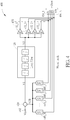
- FIG. 2 is a diagram illustrating an ADC 200 operating in the normal mode according to a second embodiment of the present invention
- FIG. 3 is a diagram illustrating the ADC 200 operating in the low power mode according to the second embodiment of the present invention.
- the ADC 200 is a sigma-delta modulator ADC
- the ADC 200 comprises an input terminal 202, a receiving circuit 210, a loop filter 220, a quantizer 230, a plurality of output terminals 204_1-204_N, and a plurality of digital-to-analog converters (DACs) 240_1-240_N.
- DACs digital-to-analog converters
- the input terminal 202 is arranged to receive an input signal Vin.
- the receiving circuit 210 is arranged to subtract a feedback signal VFB from the input signal Vin to generate a first signal V1.
- the loop filter 220 comprises a plurality of integrators connected in series, and the loop filter 220 is configured to filter the first signal V1 to generate a filtered signal V1'.
- the quantizer 230 is configured to generate the digital output signal Dout according to the filtered signal V1'.
- the DACs 240_1-240_N are coupled to the output terminals 204_1-204_N, respectively, and each of the DACs 240_1-240_N receives one bit of the corresponding output terminal, if any, to generate an analog signal, and a summation of the analog signals of the DACs 240_1-240_N serves as the feedback signal VFB.
- the quantizer 230 when the ADC 200 operates in the normal mode, the quantizer 230 generates the digital output signal Dout having N bits (i.e. the digital output signal Dout comprises the bits B1-BN), and all of the DACs 240_1-240_N are enabled to receive the bits B1-BN to generate the analog signals, respectively.
- the quantizer 230 when the ADC 200 operates in the low power mode, the quantizer 230 generates the digital output signal Dout having only one bit B1, and only the DAC 240_1 is enabled to receive the bit B1 to generate the corresponding analog signal serving as the feedback signal VFB.
- the embodiment shown in FIG. 3 because the low power mode can be simply achieved by disabling a portions of elements within the quantizer 230 and disabling a portion of the DACs 240_1-240_N, and the bit B1 is utilized to represent the input signal Vin because the amplitude of the input signal Vin becomes smaller in the low power mode, the embodiment can lower the design efforts of the multi-mode applications of the ADC.
- the order of the loop filter 220 i.e. the number of the enabled integrators within the loop filter 220
- a clock frequency used by the quantizer 230 are not changed in the normal mode and the low power mode. That is the ADC 200 uses the same order of the loop filter 220 and the clock frequency of the quantizer 230 in the normal mode and low power mode. Therefore, the ADC 200 does not need to re-synthesize the coefficients to fit the desired noise transfer function, and the design efforts and manufacturing cost can be lowered.
- a bit number of the digital output signal Dout in the low power mode is for illustratively only. As long as the bit number of the digital output signal Dout in the low power mode is less than the bit number (i.e. N) of the digital output signal Dout in the normal mode, the digital output signal Dout may have one bit, two bits or three bits in the low power mode.
- FIG. 4 is a diagram illustrating an ADC 400 operating in the normal mode according to a third embodiment of the present invention
- FIG. 5 is a diagram illustrating the ADC 400 operating in the low power mode according to the third embodiment of the present invention.
- the ADC 400 is a sigma-delta modulator ADC
- the ADC 400 comprises an input terminal 402, a receiving circuit 410, a loop filter 420, a quantizer 430, a plurality of output terminals 404_1-404_N, and a plurality of DACs 440_1-40_N
- the quantizer 430 is a flash quantizer comprising a plurality of comparators 432_1-432_N.
- the input terminal 402 is arranged to receive an input signal Vin.
- the receiving circuit 410 is arranged to subtract a feedback signal VFB from the input signal Vin to generate a first signal V1.
- the loop filter 420 comprises a plurality of integrators connected in series, and the loop filter 420 is configured to filter the first signal V1 to generate a filtered signal V1'.
- the quantizer 430 is configured to generate the digital output signal Dout according to the filtered signal V1', wherein the comparators 432_1-432_N is configured to compare the filtered signal V1' with a corresponding reference signal to generate the bits B1-BN of the digital output signal Dout, respectively.
- the DACs 440_1-440_N are coupled to the output terminals 404_1-404_N, respectively, and each of the DACs 440_1-440_N receives one bit of the corresponding output terminal, if any, to generate an analog signal, and a summation of the analog signals of the DACs 440_1-440_N serves as the feedback signal VFB.
- the order of the loop filter 420 i.e. the number of the enabled integrators within the loop filter 420
- a clock frequency used by the quantizer 430 are not changed in the normal mode and the low power mode. That is the ADC 400 uses the same the order of the loop filter 420 and the clock frequency of the quantizer 430 in the normal mode and low power mode. Therefore, the ADC 400 does not need to re-synthesize the coefficients to fit the desired noise transfer function, and the design efforts and manufacturing cost can be lowered.
- a bit number of the digital output signal Dout in the low power mode is for illustratively only. As long as the bit number of the digital output signal Dout in the low power mode is less than the bit number (i.e. N) of the digital output signal Dout in the normal mode, the digital output signal Dout may have one bit, two bits or three bits in the low power mode.
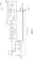
- FIG. 6 is a diagram illustrating an ADC 600 operating in the normal mode according to a fourth embodiment of the present invention
- FIG. 7 is a diagram illustrating the ADC 600 operating in the low power mode according to the fourth embodiment of the present invention.
- the ADC 600 comprises an input terminal 602, a receiving circuit 610, a loop filter 620, a quantizer 630, a plurality of output terminals 604_1-604_N, and a plurality of DACs 640_1-640_N.
- the ADC 600 is a sigma-delta modulator ADC
- the quantizer 630 is a successive approximation register (SAR) quantizer.
- the quantizer 630 comprises a plurality of capacitors C1-CK, a comparator 632 and a control logic 634.
- the input terminal 602 is arranged to receive an input signal Vin.
- the receiving circuit 610 is arranged to subtract a feedback signal VFB from the input signal Vin to generate a first signal V1.
- the loop filter 620 comprises a plurality of integrators connected in series, and the loop filter 620 is configured to filter the first signal V1 to generate a filtered signal V1'.
- the quantizer 630 is configured to generate the digital output signal Dout according to the filtered signal V1'.
- a first node of each of the capacitors is controlled to connect to the filtered signal V1', a reference signal Vref or a ground voltage according to a control signal to sample the filtered signal V1' to generate a sampled signal; the comparator 632 compares the sampled signal with another reference signal to generate a comparison result, and the control logic 634 generates the digital output signal Dout, and further generates the control signals to control the capacitors C1-CK according to the comparison result.
- the DACs 640_1-640_N are coupled to the output terminals 604_1-604_N, respectively, and each of the DACs 640_1-640_N receives one bit of the corresponding output terminal, if any, to generate an analog signal, and a summation of the analog signals of the DACs 640_1-640_N serves as the feedback signal VFB.
- the order of the loop filter 620 i.e. the number of the enabled integrators within the loop filter 620
- a clock frequency used by the quantizer 630 are not changed in the normal mode and the low power mode. That is the ADC 600 uses the same the order of the loop filter 620 and the clock frequency of the quantizer 630 in the normal mode and low power mode. Therefore, the ADC 600 does not need to re-synthesize the coefficients to fit the desired noise transfer function, and the design efforts and manufacturing cost can be lowered.
- a bit number of the digital output signal Dout in the low power mode is for illustratively only. As long as the bit number of the digital output signal Dout in the low power mode is less than the bit number (i.e. N) of the digital output signal Dout in the normal mode, the digital output signal Dout may have one bit, two bits or three bits in the low power mode.
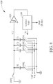
- FIG. 8 is a diagram illustrating an ADC 800 operating in the normal mode according to a fifth embodiment of the present invention
- FIG. 9 is a diagram illustrating the ADC 800 operating in the low power mode according to the fifth embodiment of the present invention. As shown in FIG. 8
- the ADC 800 is a SAR ADC, and the ADC 800 comprises a plurality of capacitors C1-CK, a plurality of switches SW1-SWK, a comparator 820 and a control logic 830, where a first node of each of the capacitors C1-CK is controlled to connect to the input signal Vin, a reference signal Vref or a ground voltage via the corresponding switch SW1-SWK, second nodes of the capacitors C1-CK are connected together, and the second nodes of the capacitors C1-CK are selectively connected to the ground voltage via a switch SW0.
- the capacitors C1-CK are controlled connect to the input signal Vin, the reference signal Vref or the ground voltage, to sample the input signal Vin to generate the sampled signal V1.
- the comparator 820 compares the sampled signal V1 with another reference voltage to generate the comparison result.
- the control logic 830 generates the digital output signal Dout having N bits, and further generates the control signals Vc to control the switches SW1-SWK for sampling the input signal Vin in a next cycle according to the comparison result.
- the ADCs 100, 200, 400, 600 and 800 are not limited to receive only one input signal Vin shown in FIGs. 1-9 . In other embodiments, the ADC 100, 200, 400, 600 or 800 may receive one or more input signals to generate the digital output signal.
- the ADC can simply reduce the bit number of the digital output signal to achieve the low power application.
- the digital output signal having less bits is sufficient to represent the input signal because the amplitude of the input signal Vin becomes smaller in the low power mode, the embodiments of the present invention indeed lower the design efforts of the multi-mode applications of the ADC without losing performance.
Landscapes
- Engineering & Computer Science (AREA)
- Theoretical Computer Science (AREA)
- Analogue/Digital Conversion (AREA)
- Compression, Expansion, Code Conversion, And Decoders (AREA)
Abstract
Description
- This application claims the priority of
US Provisional Application No. 62/622,221, filed on January 26th, 2018 - Many electronic devices, such as cellular phones, have an analog-to-digital converter (ADC) supporting a normal mode and a low power mode. In the multi-mode ADC applications, the conventional ADC is controlled to lower an order of a loop filter or lower a clock frequency of the ADC to achieve the low power application. However, the method of lowering the order of the loop filter needs to re-synthesize the coefficients to fit the desired noise transfer function, and the method of lowering the clock frequency needs large area for loop filter capacitors, or a mixed system is required to take care of the two clock frequencies. Therefore, the conventional control method of the ADC is not straightforward, time consuming and complicated.
- It is therefore an objective of the present invention to provide an ADC, which can operate in the low power mode by simply reducing quantizer/ADC bits, to solve the above-mentioned problems.
- According to one embodiment of the present invention, an ADC is provided for receiving at least an input signal to generate a digital output signal, wherein the ADC includes an input terminal and a plurality of output terminals, the input terminal is arranged to receive the input signal, and each of the output terminals is configured to output one bit of the digital output signal. The ADC is controlled to operate in a normal mode or a low power mode, and when the ADC operates in the normal mode, all of the output terminals are enabled to output the bits to form the digital output signal; and when the ADC operates in the low power mode, only a portion of the output terminals are enabled to output the bits to form the digital output signal.
- According to another embodiment of the present invention, a control method of an ADC comprises the steps of: when the ADC operates in a normal mode, controlling the ADC to receiving at least an input signal to generate a digital output signal having N bits; and when the ADC operates in a low power mode, controlling the ADC to receiving the input signal to generate the digital output signal having M bits, wherein M is less than N.
- These and other objectives of the present invention will no doubt become obvious to those of ordinary skill in the art after reading the following detailed description of the preferred embodiment that is illustrated in the various figures and drawings.
-
-
FIG. 1 is a diagram illustrating an ADC operating in the normal mode and the low power mode according to a first embodiment of the present invention. -
FIG. 2 is a diagram illustrating an ADC operating in the normal mode according to a second embodiment of the present invention. -
FIG. 3 is a diagram illustrating the ADC operating in the low power mode according to the second embodiment of the present invention. -
FIG. 4 is a diagram illustrating an ADC operating in the normal mode according to a third embodiment of the present invention. -
FIG. 5 is a diagram illustrating the ADC operating in the low power mode according to the third embodiment of the present invention. -
FIG. 6 is a diagram illustrating an ADC operating in the normal mode according to a fourth embodiment of the present invention. -
FIG. 7 is a diagram illustrating the ADC operating in the low power mode according to the fourth embodiment of the present invention. -
FIG. 8 is a diagram illustrating an ADC operating in the normal mode according to a fifth embodiment of the present invention. -
FIG. 9 is a diagram illustrating the ADC operating in the low power mode according to the fifth embodiment of the present invention. - Certain terms are used throughout the following description and claims to refer to particular system components. As one skilled in the art will appreciate, manufacturers may refer to a component by different names. This document does not intend to distinguish between components that differ in name but not function. In the following discussion and in the claims, the terms "including" and "comprising" are used in an open-ended fashion, and thus should be interpreted to mean "including, but not limited to ...". The terms "couple" and "couples" are intended to mean either an indirect or a direct electrical connection. Thus, if a first device couples to a second device, that connection may be through a direct electrical connection, or through an indirect electrical connection via other devices and connections.
-
FIG. 1 is a diagram illustrating anADC 100 operating in the normal mode and the low power mode according to a first embodiment of the present invention. As shown inFIG. 1 , theADC 100 comprises aninput terminal 110 and a plurality of output terminals 120_1-120_N, where theinput terminal 110 is arranged to receive an input signal (analog signal) Vin, and the output terminals 120_1-120_N are arranged to generate bits B1-BN, respectively. - When the ADC 100 operates in the normal mode, all of the output terminals 120_1-120_N are enabled to generate the bits B1-BN, respectively, that is the
ADC 110 generates a digital output signal Dout having N bits (i.e. B1-BN). In addition, when the ADC 100 operates in the low power mode, because an amplitude of the input signal Vin becomes smaller, only a portion of the bits are utilized to represent the input signal Vin, so a portion of elements within theADC 100 can be disabled to not generate the corresponding bits. In the embodiment shown inFIG. 1 , theADC 100 generates the digital output signal Dout having only one bit B1, and the other output terminals 120_2-120_N are disabled. - It is noted that a bit number of the digital output signal Dout in the low power mode is for illustratively only. As long as the bit number of the digital output signal Dout in the low power mode is less than the bit number (i.e. N) of the digital output signal Dout in the normal mode, the digital output signal Dout may have one bit, two bits or three bits in the low power mode.
-
FIG. 2 is a diagram illustrating anADC 200 operating in the normal mode according to a second embodiment of the present invention, andFIG. 3 is a diagram illustrating the ADC 200 operating in the low power mode according to the second embodiment of the present invention. As shown inFIG. 2 , the ADC 200 is a sigma-delta modulator ADC, and the ADC 200 comprises aninput terminal 202, areceiving circuit 210, aloop filter 220, aquantizer 230, a plurality of output terminals 204_1-204_N, and a plurality of digital-to-analog converters (DACs) 240_1-240_N. - In the operations of the
ADC 200, theinput terminal 202 is arranged to receive an input signal Vin. Thereceiving circuit 210 is arranged to subtract a feedback signal VFB from the input signal Vin to generate a first signal V1. Theloop filter 220 comprises a plurality of integrators connected in series, and theloop filter 220 is configured to filter the first signal V1 to generate a filtered signal V1'. Thequantizer 230 is configured to generate the digital output signal Dout according to the filtered signal V1'. The DACs 240_1-240_N are coupled to the output terminals 204_1-204_N, respectively, and each of the DACs 240_1-240_N receives one bit of the corresponding output terminal, if any, to generate an analog signal, and a summation of the analog signals of the DACs 240_1-240_N serves as the feedback signal VFB. - In the embodiment shown in
FIG. 2 , when the ADC 200 operates in the normal mode, thequantizer 230 generates the digital output signal Dout having N bits (i.e. the digital output signal Dout comprises the bits B1-BN), and all of the DACs 240_1-240_N are enabled to receive the bits B1-BN to generate the analog signals, respectively. In the embodiment shown inFIG. 3 , when the ADC 200 operates in the low power mode, thequantizer 230 generates the digital output signal Dout having only one bit B1, and only the DAC 240_1 is enabled to receive the bit B1 to generate the corresponding analog signal serving as the feedback signal VFB. - In the embodiment shown in
FIG. 3 , because the low power mode can be simply achieved by disabling a portions of elements within thequantizer 230 and disabling a portion of the DACs 240_1-240_N, and the bit B1 is utilized to represent the input signal Vin because the amplitude of the input signal Vin becomes smaller in the low power mode, the embodiment can lower the design efforts of the multi-mode applications of the ADC. - In one embodiment, the order of the loop filter 220 (i.e. the number of the enabled integrators within the loop filter 220) and a clock frequency used by the
quantizer 230 are not changed in the normal mode and the low power mode. That is the ADC 200 uses the same order of theloop filter 220 and the clock frequency of thequantizer 230 in the normal mode and low power mode. Therefore, the ADC 200 does not need to re-synthesize the coefficients to fit the desired noise transfer function, and the design efforts and manufacturing cost can be lowered. - It is noted that a bit number of the digital output signal Dout in the low power mode is for illustratively only. As long as the bit number of the digital output signal Dout in the low power mode is less than the bit number (i.e. N) of the digital output signal Dout in the normal mode, the digital output signal Dout may have one bit, two bits or three bits in the low power mode.
-
FIG. 4 is a diagram illustrating an ADC 400 operating in the normal mode according to a third embodiment of the present invention, andFIG. 5 is a diagram illustrating the ADC 400 operating in the low power mode according to the third embodiment of the present invention. As shown inFIG. 4 , the ADC 400 is a sigma-delta modulator ADC, and the ADC 400 comprises aninput terminal 402, areceiving circuit 410, aloop filter 420, aquantizer 430, a plurality of output terminals 404_1-404_N, and a plurality of DACs 440_1-40_N, wherein thequantizer 430 is a flash quantizer comprising a plurality of comparators 432_1-432_N. - In the operations of the
ADC 400, theinput terminal 402 is arranged to receive an input signal Vin. Thereceiving circuit 410 is arranged to subtract a feedback signal VFB from the input signal Vin to generate a first signal V1. Theloop filter 420 comprises a plurality of integrators connected in series, and theloop filter 420 is configured to filter the first signal V1 to generate a filtered signal V1'. Thequantizer 430 is configured to generate the digital output signal Dout according to the filtered signal V1', wherein the comparators 432_1-432_N is configured to compare the filtered signal V1' with a corresponding reference signal to generate the bits B1-BN of the digital output signal Dout, respectively. The DACs 440_1-440_N are coupled to the output terminals 404_1-404_N, respectively, and each of the DACs 440_1-440_N receives one bit of the corresponding output terminal, if any, to generate an analog signal, and a summation of the analog signals of the DACs 440_1-440_N serves as the feedback signal VFB. - In the embodiment shown in
FIG. 4 , when the ADC 400 operates in the normal mode, all of the comparators 432_1-432_N within thequantizer 430 are enabled to generate the digital output signal Dout having N bits (i.e. the bits B1-BN), and all of the DACs 440_1-440_N are enabled to receive the bits B1-BN to generate the analog signals, respectively. In the embodiment shown inFIG. 5 , when the ADC 400 operates in the low power mode, only the comparator 432_1 is enabled to generate the bit B1, that is thequantizer 430 generates the digital output signal Dout having only one bit B1, and only the DAC 440_1 is enabled to receive the bit B1 to generate the corresponding analog signal serving as the feedback signal VFB. - In one embodiment, the order of the loop filter 420 (i.e. the number of the enabled integrators within the loop filter 420) and a clock frequency used by the
quantizer 430 are not changed in the normal mode and the low power mode. That is the ADC 400 uses the same the order of theloop filter 420 and the clock frequency of thequantizer 430 in the normal mode and low power mode. Therefore, theADC 400 does not need to re-synthesize the coefficients to fit the desired noise transfer function, and the design efforts and manufacturing cost can be lowered. - It is noted that a bit number of the digital output signal Dout in the low power mode is for illustratively only. As long as the bit number of the digital output signal Dout in the low power mode is less than the bit number (i.e. N) of the digital output signal Dout in the normal mode, the digital output signal Dout may have one bit, two bits or three bits in the low power mode.
-
FIG. 6 is a diagram illustrating anADC 600 operating in the normal mode according to a fourth embodiment of the present invention, andFIG. 7 is a diagram illustrating theADC 600 operating in the low power mode according to the fourth embodiment of the present invention. As shown inFIG. 6 , theADC 600 comprises aninput terminal 602, a receivingcircuit 610, aloop filter 620, aquantizer 630, a plurality of output terminals 604_1-604_N, and a plurality of DACs 640_1-640_N. In this embodiment, theADC 600 is a sigma-delta modulator ADC, and thequantizer 630 is a successive approximation register (SAR) quantizer. Thequantizer 630 comprises a plurality of capacitors C1-CK, acomparator 632 and acontrol logic 634. - In the operations of the
ADC 600, theinput terminal 602 is arranged to receive an input signal Vin. The receivingcircuit 610 is arranged to subtract a feedback signal VFB from the input signal Vin to generate a first signal V1. Theloop filter 620 comprises a plurality of integrators connected in series, and theloop filter 620 is configured to filter the first signal V1 to generate a filtered signal V1'. Thequantizer 630 is configured to generate the digital output signal Dout according to the filtered signal V1'. In detail, in the operations of thequantizer 630, a first node of each of the capacitors is controlled to connect to the filtered signal V1', a reference signal Vref or a ground voltage according to a control signal to sample the filtered signal V1' to generate a sampled signal; thecomparator 632 compares the sampled signal with another reference signal to generate a comparison result, and thecontrol logic 634 generates the digital output signal Dout, and further generates the control signals to control the capacitors C1-CK according to the comparison result. The DACs 640_1-640_N are coupled to the output terminals 604_1-604_N, respectively, and each of the DACs 640_1-640_N receives one bit of the corresponding output terminal, if any, to generate an analog signal, and a summation of the analog signals of the DACs 640_1-640_N serves as the feedback signal VFB. - In the embodiment shown in
FIG. 6 , when theADC 600 operates in the normal mode, all of the capacitors C1-CK within thequantizer 630 are used to generate the sampled signal for thecomparator 632 and thecontrol logic 634 to generate the digital output signal Dout having N bits (i.e. the bits B1-BN), and all of the DACs 640_1-640_N are enabled to receive the bits B1-BN to generate the analog signals, respectively. In the embodiment shown inFIG. 7 , when theADC 600 operates in the low power mode, only the capacitors C1 and C2 are used to generate the sampled signal, and thecontrol logic 634 generates the digital output signal Dout having only one bit B1, and only the DAC 640_1 is enabled to receive the bit B1 to generate the corresponding analog signal serving as the feedback signal VFB. - In one embodiment, the order of the loop filter 620 (i.e. the number of the enabled integrators within the loop filter 620) and a clock frequency used by the
quantizer 630 are not changed in the normal mode and the low power mode. That is theADC 600 uses the same the order of theloop filter 620 and the clock frequency of thequantizer 630 in the normal mode and low power mode. Therefore, theADC 600 does not need to re-synthesize the coefficients to fit the desired noise transfer function, and the design efforts and manufacturing cost can be lowered. - It is noted that a bit number of the digital output signal Dout in the low power mode is for illustratively only. As long as the bit number of the digital output signal Dout in the low power mode is less than the bit number (i.e. N) of the digital output signal Dout in the normal mode, the digital output signal Dout may have one bit, two bits or three bits in the low power mode.
-
FIG. 8 is a diagram illustrating anADC 800 operating in the normal mode according to a fifth embodiment of the present invention, andFIG. 9 is a diagram illustrating theADC 800 operating in the low power mode according to the fifth embodiment of the present invention. As shown inFIG. 8 , theADC 800 is a SAR ADC, and theADC 800 comprises a plurality of capacitors C1-CK, a plurality of switches SW1-SWK, acomparator 820 and acontrol logic 830, where a first node of each of the capacitors C1-CK is controlled to connect to the input signal Vin, a reference signal Vref or a ground voltage via the corresponding switch SW1-SWK, second nodes of the capacitors C1-CK are connected together, and the second nodes of the capacitors C1-CK are selectively connected to the ground voltage via a switch SW0. - In the operations of the
ADC 800, the capacitors C1-CK are controlled connect to the input signal Vin, the reference signal Vref or the ground voltage, to sample the input signal Vin to generate the sampled signal V1. Thecomparator 820 compares the sampled signal V1 with another reference voltage to generate the comparison result. Thecontrol logic 830 generates the digital output signal Dout having N bits, and further generates the control signals Vc to control the switches SW1-SWK for sampling the input signal Vin in a next cycle according to the comparison result. - In the embodiment shown in
FIG. 8 , when theADC 800 operates in the normal mode, all of the capacitors C1-CK are used to generate the sampled signal for thecomparator 820 and thecontrol logic 830 to generate the digital output signal Dout having N bits. In the embodiment shown inFIG. 9 , when theADC 800 operates in the low power mode, only the capacitors C1 and C2 are used to generate the sampled signal, and thecontrol logic 830 generates the digital output signal Dout having M bit(s), where M is less than N. - It is noted that the
ADCs FIGs. 1-9 . In other embodiments, theADC - Briefly summarized, in the ADC of the present invention, the ADC can simply reduce the bit number of the digital output signal to achieve the low power application. In addition, because the digital output signal having less bits is sufficient to represent the input signal because the amplitude of the input signal Vin becomes smaller in the low power mode, the embodiments of the present invention indeed lower the design efforts of the multi-mode applications of the ADC without losing performance.
- Those skilled in the art will readily observe that numerous modifications and alterations of the device and method may be made while retaining the teachings of the invention. Accordingly, the above disclosure should be construed as limited only by the metes and bounds of the appended claims.
Claims (13)
- An analog-to-digital converter, ADC, (100, 200, 400, 600, 800) for receiving at least an input signal to generate a digital output signal, comprising:an input terminal (110, 202, 402, 602), for receiving the input signal; anda plurality of output terminals (120_1-120_N, 204_1-204_N, 404_1-404_N, 604_1-604_N), wherein each of the output terminals is configured to output one bit of the digital output signal;wherein the ADC (100, 200, 400, 600, 800) is controlled to operate in a normal mode or a low power mode, and when the ADC (100, 200, 400, 600, 800) operates in the normal mode, all of the output terminals (120_1-120_N, 204_1-204_N, 404_1-404_N, 604_1-604_N) are enabled to output the bits to form the digital output signal; and when the ADC (100, 200, 400, 600, 800) operates in the low power mode, only a portion of the output terminals (120_1-120_N, 204_1-204_N, 404_1-404_N, 604_1-604_N) are enabled to output the bits to form the digital output signal.
- The ADC (100, 200, 400, 600, 800) of claim 1, wherein a bit number of the digital output signal in the normal mode is greater than a bit number of the digital output signal in the low power mode.
- The ADC (100, 200, 400, 600, 800) of claim 1, wherein when the ADC (100, 200, 400, 600, 800) operates in the low power mode, the ADC (100, 200, 400, 600, 800) generates the digital output signal having only one bit or only two bits.
- The ADC (100, 200, 400, 600, 800) of claim 1, wherein the ADC (100, 200, 400, 600, 800) further comprises:a receiving circuit (210, 410, 610), for receiving the input signal and a feedback signal to generate a first signal;a loop filter (220, 420, 620), coupled to the receiving circuit (210, 410, 610), for filtering the first signal to generate a filtered signal;a quantizer (230, 430, 630), coupled to the loop filter (220, 420, 620) and the plurality of output terminals (120_1-120_N, 204_1-204_N, 404_1-404_N, 604_1-604_N), for generating the digital output signal according to the filtered signal; anda plurality of digital-to-analog converters, DACs, (240_1-240_N, 440_1-440_N, 640_1-640_N) coupled to the plurality of output terminals (120_1-120_N, 204_1-204_N, 404_1-404_N, 604_1-604_N), respectively, wherein each of the DACs (240_1-240_N, 440_1-440_N, 640_1-640_N) receives one bit of the corresponding output terminal to generate an analog signal, and a summation of the analog signals of the DACs (240_1-240_N, 440_1-440_N, 640_1-640_N) serves as the feedback signal;wherein the quantizer (230, 430, 630) is configured to generate the digital output signal having different bits according to the normal mode or the low power mode of the ADC (100, 200, 400, 600, 800).
- The ADC (100, 200, 400, 600, 800) of claim 4, wherein at least a portion of the DACs (240_1-240_N, 440_1-440_N, 640_1-640_N) are controlled to be enabled or disabled according to the normal mode or the low power mode of the ADC (100, 200, 400, 600, 800).
- The ADC (100, 200, 400, 600, 800) of claim 5, wherein when the ADC (100, 200, 400, 600, 800) operates in the normal mode, the quantizer (230, 430, 630) is configured to generate the digital output signal having N bits, and all of the DACs (240_1-240_N, 440_1-440_N, 640_1-640_N) are enabled to generate the analog signals, respectively; and when the ADC (100, 200, 400, 600, 800) operates in the low power mode, the quantizer (230, 430, 630) is configured to generate the digital output signal having M bits, and only a portion of the DACs (240_1-240_N, 440_1-440_N, 640_1-640_N) are enabled to generate the analog signal (s), wherein M is less than N.
- The ADC (100, 200, 400, 600, 800) of claim 4, wherein the quantizer (230, 430, 630) comprises a plurality of comparators (432_1-432_N), each comparator is configured to generate one bit of the digital output signal, and at least a portion of the comparators (432_1-432_N) are controlled to be enabled or disabled according to the normal mode or the low power mode of the ADC (100, 200, 400, 600, 800).
- The ADC (100, 200, 400, 600, 800) of claim 4, wherein the quantizer (230, 430, 630) is a successive approximation register (SAR) quantizer (230, 430, 630), and the quantizer (230, 430, 630) comprises:a plurality of capacitors (C1-CK), wherein a first node of each of the capacitors (C1-CK) is controlled to connect to the filtered signal or a reference signal according to a control signal, to sample the filtered signal to generate a sampled signal;a comparator (632, 820), for comparing the sampled signal with another reference signal to generate a comparison result; anda control logic (634, 830), for generating the digital output signal, and further generating the control signals to control the plurality of capacitors according to the comparison result;wherein at least a portion of the capacitors are controlled to be enabled or disabled according to the normal mode or the low power mode of the ADC (100, 200, 400, 600, 800).
- The ADC (100, 200, 400, 600, 800) of claim 4, wherein an order of the loop filter (220, 420, 620) or a frequency of a clock signal used by the quantizer (230, 430, 630) is not changed according to the normal mode or the low power mode of the ADC (100, 200, 400, 600, 800).
- The ADC (100, 200, 400, 600, 800) of claim 1, wherein the ADC (100, 200, 400, 600, 800) is a SAR ADC, and the ADC (100, 200, 400, 600, 800) further comprises:a plurality of capacitors (C1-CK), wherein a first node of each of the capacitors is controlled to connect to the input signal or a reference signal according to a control signal, to sample the input signal to generate a sampled signal;a comparator (632, 820), for comparing the sampled signal with another reference signal to generate a comparison result; anda control logic (634, 830), for generating the digital output signal, and further generating the control signals to control the plurality of capacitors (C1-CK) according to the comparison result;wherein the control logic (634, 830) is configured to generate the digital output signal having different bits according to the normal mode or the low power mode of the ADC.
- The ADC (100, 200, 400, 600, 800) of claim 10, wherein at least a portion of the capacitors are controlled to be enabled or disabled according to the normal mode or the low power mode of the ADC (100, 200, 400, 600, 800).
- A control method of an analog-to-digital converter, ADC, (100, 200, 400, 600, 800) comprising:when the ADC (100, 200, 400, 600, 800) operates in a normal mode, controlling the ADC (100, 200, 400, 600, 800) to receiving at least an input signal to generate a digital output signal having N bits; andwhen the ADC (100, 200, 400, 600, 800) operates in a low power mode, controlling the ADC (100, 200, 400, 600, 800) to receiving the input signal to generate the digital output signal having M bits, wherein M is less than N.
- The control method of claim 12, wherein M is equal to one or two.
Applications Claiming Priority (2)
| Application Number | Priority Date | Filing Date | Title |
|---|---|---|---|
| US201862622221P | 2018-01-26 | 2018-01-26 | |
| US16/188,217 US10944418B2 (en) | 2018-01-26 | 2018-11-12 | Analog-to-digital converter capable of generate digital output signal having different bits |
Publications (1)
| Publication Number | Publication Date |
|---|---|
| EP3518424A1 true EP3518424A1 (en) | 2019-07-31 |
Family
ID=64664177
Family Applications (1)
| Application Number | Title | Priority Date | Filing Date |
|---|---|---|---|
| EP18211372.0A Ceased EP3518424A1 (en) | 2018-01-26 | 2018-12-10 | Analog-to-digital converter capable of generate digital output signal having different bits |
Country Status (4)
| Country | Link |
|---|---|
| US (1) | US10944418B2 (en) |
| EP (1) | EP3518424A1 (en) |
| CN (1) | CN110086470A (en) |
| TW (1) | TW201933787A (en) |
Families Citing this family (7)
| Publication number | Priority date | Publication date | Assignee | Title |
|---|---|---|---|---|
| US11121720B2 (en) * | 2019-08-07 | 2021-09-14 | Mediatek Inc. | Analog-to-digital converter having quantization error duplicate mechanism |
| CN112491417B (en) * | 2019-09-12 | 2024-12-27 | 瑞昱半导体股份有限公司 | Analog-to-digital converter |
| US20210376844A1 (en) * | 2020-06-02 | 2021-12-02 | Short Circuit Technologies Llc | Event Driven Quasi-Level Crossing Delta Modulator Analog To Digital Converter With Adaptive Resolution |
| US11863196B2 (en) | 2021-12-03 | 2024-01-02 | Infineon Technologies Ag | Microphones with an on-demand digital-to-analog converter |
| EP4498606A4 (en) * | 2022-05-20 | 2025-05-07 | Mitsubishi Electric Corporation | DELTA-SIGMA MODULATION CIRCUIT, DIGITAL TRANSMISSION CIRCUIT AND DIGITAL TRANSMITTER |
| US11990917B2 (en) * | 2022-06-07 | 2024-05-21 | Invensense, Inc. | Incremental analog to digital converter incorporating noise shaping and residual error quantization |
| US12074577B2 (en) * | 2022-06-27 | 2024-08-27 | Renesas Design Technology Inc. | Active filter |
Citations (1)
| Publication number | Priority date | Publication date | Assignee | Title |
|---|---|---|---|---|
| US6894632B1 (en) * | 2004-01-14 | 2005-05-17 | Northrop Grumman Corporation | Programmable analog-to-digital converter |
Family Cites Families (22)
| Publication number | Priority date | Publication date | Assignee | Title |
|---|---|---|---|---|
| US5369403A (en) | 1992-09-01 | 1994-11-29 | The State Of Oregon Acting By And Through The State Board Of Higher Education On Behalf Of Oregon State University | Dual quantization oversampling digital-to-analog converter |
| US7171542B1 (en) | 2000-06-19 | 2007-01-30 | Silicon Labs Cp, Inc. | Reconfigurable interface for coupling functional input/output blocks to limited number of i/o pins |
| US6362762B1 (en) | 2000-08-23 | 2002-03-26 | Hrl Laboratories, Llc | Multiple mode analog-to-digital converter employing a single quantizer |
| US6642873B1 (en) * | 2002-06-03 | 2003-11-04 | Wensheng Vincent Kuang | Multi-level D/A converter incorporated with multi-level quantizer in multi-bit sigma-delta A/D converter |
| US6674381B1 (en) * | 2003-02-28 | 2004-01-06 | Texas Instruments Incorporated | Methods and apparatus for tone reduction in sigma delta modulators |
| RU2316059C2 (en) | 2003-05-01 | 2008-01-27 | Нокиа Корпорейшн | Method and device for quantizing amplification in broadband speech encoding with alternating bitrate |
| US6980144B1 (en) | 2004-06-03 | 2005-12-27 | Texas Instruments Incorporated | Method for reducing DAC resolution in multi-bit sigma delta analog-to digital converter (ADC) |
| US7423567B2 (en) | 2006-09-12 | 2008-09-09 | Cirrus Logic, Inc. | Analog-to-digital converter (ADC) having a reduced number of quantizer output levels |
| GB2452751A (en) * | 2007-09-13 | 2009-03-18 | Iti Scotland Ltd | Analog-to-Digital Converter comprising selective comparators |
| JP4492713B2 (en) * | 2008-02-21 | 2010-06-30 | セイコーエプソン株式会社 | Integrated circuit device and electronic apparatus |
| CN102017423A (en) * | 2008-05-08 | 2011-04-13 | 松下电器产业株式会社 | Flash A/D converter, flash A/D conversion module, and delta-sigma A/D converter |
| US7656340B2 (en) * | 2008-06-06 | 2010-02-02 | Lsi Corporation | Systems and methods for pipelined analog to digital conversion |
| US8344921B2 (en) * | 2010-11-04 | 2013-01-01 | Mediatek Inc. | Sigma-delta modulator with SAR ADC and truncater having order lower than order of integrator and related sigma-delta modulation method |
| JP5965290B2 (en) * | 2012-10-31 | 2016-08-03 | ルネサスエレクトロニクス株式会社 | Analog / digital converter and self-diagnosis method of analog / digital converter |
| US9766678B2 (en) | 2013-02-04 | 2017-09-19 | Intel Corporation | Multiple voltage identification (VID) power architecture, a digital synthesizable low dropout regulator, and apparatus for improving reliability of power gates |
| US9306588B2 (en) * | 2014-04-14 | 2016-04-05 | Cirrus Logic, Inc. | Switchable secondary playback path |
| US9525428B2 (en) * | 2014-12-17 | 2016-12-20 | Analog Devices, Inc. | Randomly sampling reference ADC for calibration |
| EP3119001B1 (en) * | 2015-07-14 | 2018-05-16 | Nxp B.V. | A sigma-delta modulator |
| US9673835B1 (en) | 2015-12-04 | 2017-06-06 | Taiwan Semiconductor Manufacturing Co., Ltd. | Pipelined SAR with TDC converter |
| US10056914B2 (en) | 2015-12-18 | 2018-08-21 | Analog Devices Global | Frequency-domain ADC flash calibration |
| US20170288693A1 (en) * | 2016-04-01 | 2017-10-05 | Stmicroelectronics International N.V. | Continuous time delta-sigma modulator with a time interleaved quantization function |
| KR102653887B1 (en) * | 2017-01-31 | 2024-04-02 | 삼성전자주식회사 | Delta modulator with variable feedback gain, Analog-digital converter and Communicating device including the delta modulator |
-
2018
- 2018-11-12 US US16/188,217 patent/US10944418B2/en active Active
- 2018-12-05 CN CN201811481847.0A patent/CN110086470A/en active Pending
- 2018-12-10 EP EP18211372.0A patent/EP3518424A1/en not_active Ceased
- 2018-12-24 TW TW107146799A patent/TW201933787A/en unknown
Patent Citations (1)
| Publication number | Priority date | Publication date | Assignee | Title |
|---|---|---|---|---|
| US6894632B1 (en) * | 2004-01-14 | 2005-05-17 | Northrop Grumman Corporation | Programmable analog-to-digital converter |
Non-Patent Citations (14)
| Title |
|---|
| BETTINI LUCA ET AL: "A Reconfigurable DT $\Delta \Sigma $ Modulator for Multi-Standard 2G/3G/4G Wireless Receivers", IEEE JOURNAL ON EMERGING AND SELECTED TOPICS IN CIRCUITS AND SYSTEMS, IEEE, PISCATAWAY, NJ, USA, vol. 5, no. 4, 1 December 2015 (2015-12-01), pages 525 - 536, XP011595141, ISSN: 2156-3357, [retrieved on 20151221], DOI: 10.1109/JETCAS.2015.2502162 * |
| CHAO I-JEN ET AL: "A Single Opamp Third-Order Low-Distortion Delta-Sigma Modulator with SAR Quantizer Embedded Passive Adder", IEICE TRANSACTIONS ON ELECTRONICS, vol. E97.C, no. 6, 1 June 2014 (2014-06-01), Tokyo, JP., pages 526 - 537, XP093121289, ISSN: 0916-8524, Retrieved from the Internet <URL:https://search.ieice.org/bin/pdf_link.php?category=C&lang=E&year=2014&fname=e97-c_6_526&abst=> DOI: 10.1587/transele.E97.C.526 * |
| HSU TIEN-FENG ET AL: "A first-order low distortion sigma-delta modulator using split DWA technique and SAR quantizer", VLSI DESIGN, AUTOMATION AND TEST(VLSI-DAT), IEEE, 27 April 2015 (2015-04-27), pages 1 - 4, XP032781544, DOI: 10.1109/VLSI-DAT.2015.7114518 * |
| ISHIZUKA MOTOMI ET AL: "Design of resource sharing reconfigurable [Delta][Sigma] SAR-ADC", 2018 23RD ASIA AND SOUTH PACIFIC DESIGN AUTOMATION CONFERENCE (ASP-DAC), IEEE, 22 January 2018 (2018-01-22), pages 317 - 318, XP033323820, DOI: 10.1109/ASPDAC.2018.8297338 * |
| LEE SANG HYEON: "High efficiency wideband low-power delta-sigma modulators", 29 May 2012 (2012-05-29), Oregon State University, USA, pages 1 - 108, XP093120061, Retrieved from the Internet <URL:https://ir.library.oregonstate.edu/downloads/0z7091967?locale=en> [retrieved on 20240116] * |
| LEOW YOON HWEE ET AL: "A 1 V 103 dB 3rd-Order Audio Continuous-Time $\Delta \Sigma $ ADC With Enhanced Noise Shaping in 65 nm CMOS", IEEE JOURNAL OF SOLID-STATE CIRCUITS, IEEE, USA, vol. 51, no. 11, 1 November 2016 (2016-11-01), pages 2625 - 2638, XP011626616, ISSN: 0018-9200, [retrieved on 20161024], DOI: 10.1109/JSSC.2016.2593777 * |
| MARCUS YIP ET AL: "A Resolution-Reconfigurable 5-to-10-Bit 0.4-to-1 V Power Scalable SAR ADC for Sensor Applications", IEEE JOURNAL OF SOLID-STATE CIRCUITS, IEEE SERVICE CENTER, PISCATAWAY, NJ, USA, vol. 48, no. 6, 1 June 2013 (2013-06-01), pages 1453 - 1464, XP011510724, ISSN: 0018-9200, DOI: 10.1109/JSSC.2013.2254551 * |
| MOHAMMAD RANJBAR ET AL: "A 3.1 mW Continuous-Time [Delta][Sigma] Modulator With 5-Bit Successive Approximation Quantizer for WCDMA", IEEE JOURNAL OF SOLID-STATE CIRCUITS, IEEE, USA, vol. 45, no. 8, 1 August 2010 (2010-08-01), pages 1479 - 1491, XP011314250, ISSN: 0018-9200, DOI: 10.1109/JSSC.2010.2047423 * |
| PAN CHUNIHUI ET AL: "A 2nd-order Delta Sigma AD modulator using dynamic amplifier and dynamic SAR quantizer", 2016 INTERNATIONAL SYMPOSIUM ON INTELLIGENT SIGNAL PROCESSING AND COMMUNICATION SYSTEMS (ISPACS), IEEE, 24 October 2016 (2016-10-24), pages 1 - 5, XP033047677, DOI: 10.1109/ISPACS.2016.7824725 * |
| PIETER HARPE ET AL: "A 0.7V 7-to-10bit 0-to-2MS/s flexible SAR ADC for ultra low-power wireless sensor nodes", ESSCIRC (ESSCIRC), 2012 PROCEEDINGS OF THE, IEEE, 17 September 2012 (2012-09-17), pages 373 - 376, XP032466549, ISBN: 978-1-4673-2212-6, DOI: 10.1109/ESSCIRC.2012.6341363 * |
| PIETER HARPE ET AL: "A 7-to-10b 0-to-4MS/s flexible SAR ADC with 6.5-to-16fJ/conversion-step", SOLID-STATE CIRCUITS CONFERENCE DIGEST OF TECHNICAL PAPERS (ISSCC), 2012 IEEE INTERNATIONAL, IEEE, 19 February 2012 (2012-02-19), pages 472 - 474, XP032154548, ISBN: 978-1-4673-0376-7, DOI: 10.1109/ISSCC.2012.6177096 * |
| RADJEN DEJAN ET AL: "A low-power 2nd-order CT [Delta][Sigma] modulator with an asynchronous SAR q", 2014 NORCHIP, IEEE, 27 October 2014 (2014-10-27), pages 1 - 4, XP032715656, DOI: 10.1109/NORCHIP.2014.7004726 * |
| SREEHARI VEERAMACHANEN ET AL: "Design of a Low Power, Variable-Resolution Flash ADC", VLSI DESIGN, 2009 22ND INTERNATIONAL CONFERENCE ON, IEEE, PISCATAWAY, NJ, USA, 5 January 2009 (2009-01-05), pages 117 - 122, XP031406905, ISBN: 978-0-7695-3506-7 * |
| ZHU ZHANGMING ET AL: "A 6-to-10-Bit 0.5 V-to-0.9 V Reconfigurable 2 MS/s Power Scalable SAR ADC in 0.18 $\mu{\rm m}$ CMOS", IEEE TRANSACTIONS ON CIRCUITS AND SYSTEMS I: REGULAR PAPERS, IEEE, US, vol. 62, no. 3, 1 March 2015 (2015-03-01), pages 689 - 696, XP011573900, ISSN: 1549-8328, [retrieved on 20150223], DOI: 10.1109/TCSI.2014.2377431 * |
Also Published As
| Publication number | Publication date |
|---|---|
| US20190238151A1 (en) | 2019-08-01 |
| CN110086470A (en) | 2019-08-02 |
| US10944418B2 (en) | 2021-03-09 |
| TW201933787A (en) | 2019-08-16 |
Similar Documents
| Publication | Publication Date | Title |
|---|---|---|
| US10944418B2 (en) | Analog-to-digital converter capable of generate digital output signal having different bits | |
| EP2430760B1 (en) | Sigma-delta converters and methods for analog-to-digital conversion | |
| US5892472A (en) | Processor controlled analog-to-digital converter circuit | |
| US7551114B2 (en) | Reducing power consumption in the early stages of a pipeline sub-ADC used in a time-interleaved ADC | |
| EP1066684B1 (en) | Circuit and method for reducing sampling noise | |
| CN109818620B (en) | Reconfigurable Sigma-Delta modulator | |
| US20080180299A1 (en) | Class D Analog-to-Digital Converter | |
| KR20010075390A (en) | Variable order sigma-delta modulator | |
| EP3772825B1 (en) | Analog-to-digital converter having quantization error duplicate mechanism | |
| US7796071B2 (en) | Processing signals of a capacitive feedforward filter | |
| CN114584149B (en) | Analog-to-digital converter | |
| US10763875B2 (en) | Switched capacitor circuit and analog-to-digital converter device | |
| US8462030B2 (en) | Programmable loop filter for use with a sigma delta analog-to-digital converter and method of programming the same | |
| van Veldhoven | A tri-mode continuous-time/spl Sigma//spl Delta/modulator with switched-capacitor feedback DAC for a GSM-EDGE/CDMA2000/UMTS receiver | |
| EP3490152A1 (en) | Interleaving quantizer in continuous-time delta-sigma modulator for quantization level increment | |
| US8441384B2 (en) | Switched-capacitor circuit with low signal degradation | |
| KR20190021634A (en) | Discrete-time integrator circuit with operational amplifier gain compensation function | |
| CN101313473A (en) | Provides a reference voltage with the desired accuracy for dynamically changing loads for short durations | |
| US12592717B2 (en) | Integrator circuit | |
| US20260118903A1 (en) | Low-noise and fast-settling reference voltage generator for capacitive digital-to-analog converter | |
| US9628103B2 (en) | Multi-mode discrete-time delta-sigma modulator power optimization using split-integrator scheme | |
| SE518012C2 (en) | Sigma-Delta Modulator in front receiver and A / D converter including such and a method for signal processing | |
| US5760728A (en) | Input stage for an analog-to-digital converter and method of operation thereof | |
| TWI768931B (en) | Analog circuit and comparator sharing method of analog circuit | |
| Maheshwari et al. | Companding baseband switched capacitor filters and ADCs for WLAN applications |
Legal Events
| Date | Code | Title | Description |
|---|---|---|---|
| PUAI | Public reference made under article 153(3) epc to a published international application that has entered the european phase |
Free format text: ORIGINAL CODE: 0009012 |
|
| STAA | Information on the status of an ep patent application or granted ep patent |
Free format text: STATUS: THE APPLICATION HAS BEEN PUBLISHED |
|
| AK | Designated contracting states |
Kind code of ref document: A1 Designated state(s): AL AT BE BG CH CY CZ DE DK EE ES FI FR GB GR HR HU IE IS IT LI LT LU LV MC MK MT NL NO PL PT RO RS SE SI SK SM TR |
|
| AX | Request for extension of the european patent |
Extension state: BA ME |
|
| STAA | Information on the status of an ep patent application or granted ep patent |
Free format text: STATUS: REQUEST FOR EXAMINATION WAS MADE |
|
| 17P | Request for examination filed |
Effective date: 20191216 |
|
| RBV | Designated contracting states (corrected) |
Designated state(s): AL AT BE BG CH CY CZ DE DK EE ES FI FR GB GR HR HU IE IS IT LI LT LU LV MC MK MT NL NO PL PT RO RS SE SI SK SM TR |
|
| STAA | Information on the status of an ep patent application or granted ep patent |
Free format text: STATUS: EXAMINATION IS IN PROGRESS |
|
| 17Q | First examination report despatched |
Effective date: 20211012 |
|
| P01 | Opt-out of the competence of the unified patent court (upc) registered |
Effective date: 20230607 |
|
| STAA | Information on the status of an ep patent application or granted ep patent |
Free format text: STATUS: THE APPLICATION HAS BEEN REFUSED |
|
| 18R | Application refused |
Effective date: 20240728 |