EP3518239A1 - Adjustable storage device carrier - Google Patents
Adjustable storage device carrier Download PDFInfo
- Publication number
- EP3518239A1 EP3518239A1 EP19150238.4A EP19150238A EP3518239A1 EP 3518239 A1 EP3518239 A1 EP 3518239A1 EP 19150238 A EP19150238 A EP 19150238A EP 3518239 A1 EP3518239 A1 EP 3518239A1
- Authority
- EP
- European Patent Office
- Prior art keywords
- storage device
- carrier
- holding element
- device carrier
- thickness
- Prior art date
- Legal status (The legal status is an assumption and is not a legal conclusion. Google has not performed a legal analysis and makes no representation as to the accuracy of the status listed.)
- Granted
Links
Images


Classifications
-
- G—PHYSICS
- G11—INFORMATION STORAGE
- G11B—INFORMATION STORAGE BASED ON RELATIVE MOVEMENT BETWEEN RECORD CARRIER AND TRANSDUCER
- G11B33/00—Constructional parts, details or accessories not provided for in the other groups of this subclass
- G11B33/12—Disposition of constructional parts in the apparatus, e.g. of power supply, of modules
- G11B33/121—Disposition of constructional parts in the apparatus, e.g. of power supply, of modules the apparatus comprising a single recording/reproducing device
- G11B33/123—Mounting arrangements of constructional parts onto a chassis
- G11B33/124—Mounting arrangements of constructional parts onto a chassis of the single recording/reproducing device, e.g. disk drive, onto a chassis
-
- B—PERFORMING OPERATIONS; TRANSPORTING
- B65—CONVEYING; PACKING; STORING; HANDLING THIN OR FILAMENTARY MATERIAL
- B65D—CONTAINERS FOR STORAGE OR TRANSPORT OF ARTICLES OR MATERIALS, e.g. BAGS, BARRELS, BOTTLES, BOXES, CANS, CARTONS, CRATES, DRUMS, JARS, TANKS, HOPPERS, FORWARDING CONTAINERS; ACCESSORIES, CLOSURES, OR FITTINGS THEREFOR; PACKAGING ELEMENTS; PACKAGES
- B65D61/00—External frames or supports adapted to be assembled around, or applied to, articles
-
- G—PHYSICS
- G06—COMPUTING OR CALCULATING; COUNTING
- G06F—ELECTRIC DIGITAL DATA PROCESSING
- G06F1/00—Details not covered by groups G06F3/00 - G06F13/00 and G06F21/00
- G06F1/16—Constructional details or arrangements
- G06F1/18—Packaging or power distribution
- G06F1/183—Internal mounting support structures, e.g. for supporting printed circuit boards
- G06F1/187—Mounting of fixed or removable disk drives
-
- H—ELECTRICITY
- H05—ELECTRIC TECHNIQUES NOT OTHERWISE PROVIDED FOR
- H05K—PRINTED CIRCUITS; CASINGS OR CONSTRUCTIONAL DETAILS OF ELECTRIC APPARATUS; MANUFACTURE OF ASSEMBLAGES OF ELECTRICAL COMPONENTS
- H05K7/00—Constructional details common to different types of electric apparatus
- H05K7/14—Mounting supporting structure in casing or on frame or rack
- H05K7/1401—Mounting supporting structure in casing or on frame or rack comprising clamping or extracting means
-
- G—PHYSICS
- G06—COMPUTING OR CALCULATING; COUNTING
- G06F—ELECTRIC DIGITAL DATA PROCESSING
- G06F1/00—Details not covered by groups G06F3/00 - G06F13/00 and G06F21/00
- G06F1/16—Constructional details or arrangements
Definitions
- the present disclosure is directed to a 2.5-inch storage device carrier suitable for accommodating different thicknesses of 2.5-inch storage devices.
- One manner of making the storage device carrier accommodate different thicknesses of storage devices is the use of a revolving holding element that has several different length arms to bear upon, and securely locate, the storage device within the storage device carrier.
- Common 2.5-inch storage device thicknesses are 7mm, 9.5mm, and 15mm, but current storage device carriers are suitable only for carrying storage devices having a 7mm thickness. In order to accommodate different storage device thicknesses in one carrier, and hold the storage device in a predetermined position, the structure of storage device carriers must be adjusted.
- a storage carrier and method for carrying and holding a 2.5-inch storage device in a predetermined location, irrespective of the thickness of the storage device.
- a 2.5-inch storage device carrier is provided with two walls positioned orthogonal to each other, and on each wall is provided a storage device holding element, where the storage device holding element has three different height bearing surfaces.
- the storage device holding element comprises a short and a long arm, as well as a flattened surface, such that when the storage device holding element is rotated it can securely hold storage devices of different thicknesses.
- the storage device holding element further incorporates two location holding points to prevent rotation of the storage device holding element.
- the rotatable storage device holding element can include a screw and spring to precisely position the storage device holding element in relation to the storage device.
- FIG. 1 illustrates a schematic, perspective view of a conventional 2.5-inch storage carrier 10 in which a 7mm thick storage device 12 is inserted.
- Non-adjustable holders 14, 16, hold the 7mm thick storage device 12 in position.
- FIG. 2 illustrates a schematic representation of two walls 19, 20, positioned orthogonal to each other.
- Each wall 19, 20, is fitted with a storage device holding element 23, 26, and utilizes a spring 28 and screw 29 to position the storage device holding element 23 in place.
- a similar spring 38 and screw 39 can be used to position storage device holding elements 26 in place.
- Tab 3 and two columns 4 locate the storage device to be inserted.
- FIG. 3 we will describe storage device holding element 23 in detail. However, as storage device holding elements 23 and 26 are identical in structure, the description of storage device 23 in detail will apply equally to storage device holding element 26.
- storage device holding element 23 is enlarged to show two location points 24, 25, which are illustrated in the drawings as protrusions. Location points 24, 25 cooperate with depressions 34, 35, in a wall 19 (or 20) (in FIG. 2 ) to maintain storage device holding element 23 in a fixed position, while the tension of the spring 28 (in FIG. 2 ) biases the location points 24 and 25 into the depressions 34 and 35 to lock storage device holding element 23 in a fixed position of rotation.
- FIG. 3 we will describe storage device holding element 23 in detail. However, as storage device holding elements 23 and 26 are identical in structure, the description of storage device 23 in detail will apply equally to storage device holding element 26.
- FIG. 3 storage device holding element 23 is enlarged to show two location points 24, 25, which are illustrated in the drawings as protrusions. Location points 24, 25 cooperate with depressions 34, 35
- storage device holding element 23 is provided with 3 differing height bearing surfaces. These three different bearing surfaces can be described as a long arm 21, a short arm 22, and a flat bearing surface 27. These three differing height bearing surfaces act to retain the storage devices of different thicknesses securely within the storage device carrier 30 (described below in FIGS. 4 - 6 ). In other words, the storage device holding element 23 is a rotational element with multiple bearing surfaces.
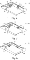
- Long arm 21 is utilized when storage device 12 (in FIG. 1 ) of 7mm thickness is placed in storage device carrier 30, which consists of a main body 31 comprised of the two orthogonal walls 19, 20, as shown in FIG. 4 .
- Short arm 22 is utilized when a storage device 32 of 9.5mm thickness is placed in storage device carrier 30, as shown in FIG. 5 .
- Flat bearing surface 27 is utilized when a storage device 42 of 15mm thickness is placed in storage device carrier 30, as shown in FIG. 6 .
- storage device holding element 26 is identical to storage device holding element 23, and is provided with the same 3 differing height bearing surfaces for use in the same manner with storage devices 12, 32, and 42 of differing thicknesses. It is also possible to provide the storage device holding element 23 (or 26) with infinitely adjustable holding power by converting the differing heights of arms and flat bearing surface into a continuously curved cam-shape, so that any thickness within the 7mm to 15mm thickness range can be securely located with the storage device carrier. Of course, different thicknesses can be accommodated in addition to, or in lieu of, the three specific thicknesses exemplified.
- one storage device carrier 30 can accommodate three different thicknesses of storage devices 12, 32, and 42, without requiring extensive modification to the storage device carrier itself.
- all that would be required is the provision of new storage device holding elements with bearing surfaces to accommodate the differing thicknesses.
Landscapes
- Engineering & Computer Science (AREA)
- Theoretical Computer Science (AREA)
- General Physics & Mathematics (AREA)
- Computer Hardware Design (AREA)
- Power Engineering (AREA)
- Human Computer Interaction (AREA)
- Physics & Mathematics (AREA)
- General Engineering & Computer Science (AREA)
- Microelectronics & Electronic Packaging (AREA)
- Mechanical Engineering (AREA)
- Details Of Rigid Or Semi-Rigid Containers (AREA)
- Container, Conveyance, Adherence, Positioning, Of Wafer (AREA)
- Packaging Frangible Articles (AREA)
- Buffer Packaging (AREA)
- Warehouses Or Storage Devices (AREA)
- Packaging Of Annular Or Rod-Shaped Articles, Wearing Apparel, Cassettes, Or The Like (AREA)
Abstract
Description
- The present disclosure is directed to a 2.5-inch storage device carrier suitable for accommodating different thicknesses of 2.5-inch storage devices. One manner of making the storage device carrier accommodate different thicknesses of storage devices is the use of a revolving holding element that has several different length arms to bear upon, and securely locate, the storage device within the storage device carrier.
- Common 2.5-inch storage device thicknesses are 7mm, 9.5mm, and 15mm, but current storage device carriers are suitable only for carrying storage devices having a 7mm thickness. In order to accommodate different storage device thicknesses in one carrier, and hold the storage device in a predetermined position, the structure of storage device carriers must be adjusted.
- In one embodiment according to the present disclosure, a storage carrier and method is provided for carrying and holding a 2.5-inch storage device in a predetermined location, irrespective of the thickness of the storage device.
- In another embodiment according to the present disclosure, a 2.5-inch storage device carrier is provided with two walls positioned orthogonal to each other, and on each wall is provided a storage device holding element, where the storage device holding element has three different height bearing surfaces.
- In a still further embodiment according to the present disclosure, the storage device holding element comprises a short and a long arm, as well as a flattened surface, such that when the storage device holding element is rotated it can securely hold storage devices of different thicknesses. In order to prevent release of the storage device from the carrier by inadvertent rotation of the storage device holding element, the storage device holding element further incorporates two location holding points to prevent rotation of the storage device holding element. The rotatable storage device holding element can include a screw and spring to precisely position the storage device holding element in relation to the storage device.
- Further particular and preferred aspects of the present invention are set out in the accompanying independent and dependent claims. Features of the dependent claims may be combined with features of the independent claims as appropriate, and in combinations other than those explicitly set out in the claims.
- The present invention will be described further, by way of example only, with reference to embodiments thereof as illustrated in the accompanying drawings, in which:
-
FIG. 1 (Prior Art) is a schematic, perspective view of an existing 2.5-inch storage carrier. -
FIG. 2 is a schematic representation of two walls positioned orthogonal to each other, with each wall fitted with a storage device holding element that utilizes a spring and screw. -
FIG. 3 is an enlarged view of the storage device holding element to show in detail, the short and long arms, as well as a flat surface, which securely hold storage devices of different thicknesses depending on the rotational position of the storage device holding element, and the two location points to prevent inadvertent rotation of the storage device holding element. -
FIG. 4 is a schematic representation of the 2.5-inch storage device carrier according to the disclosure, with a 7mm thick storage device held in place by the long arm of the storage device holding element. -
FIG. 5 is a schematic representation of the 2.5-inch storage device carrier according to the disclosure, with a 9.5mm thick storage device held in place by the short arm of the storage device holding element. -
FIG. 6 is a schematic representation of the 2.5-inch storage device carrier according to the disclosure, with a 15mm thick storage device held in place by the flat surface of the storage device holding element. - The present invention is described with reference to the attached figures, where like reference numerals are used throughout the figures to designate similar or equivalent elements. The figures are not drawn to scale and are provided merely to illustrate the instant invention. Several aspects of the invention are described below with reference to example applications for illustration. It should be understood that numerous specific details, relationships, and methods are set forth to provide a full understanding of the invention. One having ordinary skill in the relevant art, however, will readily recognize that the invention can be practiced without one or more of the specific details, or with other methods. In other instances, well-known structures or operations are not shown in detail to avoid obscuring the invention. The present invention is not limited by the illustrated ordering of acts or events, as some acts may occur in different orders and/or concurrently with other acts or events. Furthermore, not all illustrated acts or events are required to implement a methodology in accordance with the present invention.
-
FIG. 1 illustrates a schematic, perspective view of a conventional 2.5-inch storage carrier 10 in which a 7mmthick storage device 12 is inserted.Non-adjustable holders thick storage device 12 in position. There is no mechanism in thestorage device 10 ofFIG. 1 to position and hold storage devices which are 9.5 mm or 15mm in thickness. -
FIG. 2 illustrates a schematic representation of twowalls wall device holding element spring 28 and screw 29 to position the storagedevice holding element 23 in place. Asimilar spring 38 andscrew 39 can be used to position storagedevice holding elements 26 in place.Tab 3 and two columns 4 locate the storage device to be inserted. - In
FIG. 3 , we will describe storagedevice holding element 23 in detail. However, as storagedevice holding elements storage device 23 in detail will apply equally to storagedevice holding element 26. InFIG. 3 , storagedevice holding element 23 is enlarged to show twolocation points Location points depressions FIG. 2 ) to maintain storagedevice holding element 23 in a fixed position, while the tension of the spring 28 (inFIG. 2 ) biases thelocation points depressions device holding element 23 in a fixed position of rotation. As can also be appreciated inFIG. 3 , storagedevice holding element 23 is provided with 3 differing height bearing surfaces. These three different bearing surfaces can be described as along arm 21, ashort arm 22, and a flat bearingsurface 27. These three differing height bearing surfaces act to retain the storage devices of different thicknesses securely within the storage device carrier 30 (described below inFIGS. 4 - 6 ). In other words, the storagedevice holding element 23 is a rotational element with multiple bearing surfaces. -
Long arm 21 is utilized when storage device 12 (inFIG. 1 ) of 7mm thickness is placed instorage device carrier 30, which consists of amain body 31 comprised of the twoorthogonal walls FIG. 4 . -
Short arm 22 is utilized when astorage device 32 of 9.5mm thickness is placed instorage device carrier 30, as shown inFIG. 5 . - Flat bearing
surface 27 is utilized when astorage device 42 of 15mm thickness is placed instorage device carrier 30, as shown inFIG. 6 . - As shown in
FIGS. 4 - 6 , storagedevice holding element 26 is identical to storagedevice holding element 23, and is provided with the same 3 differing height bearing surfaces for use in the same manner withstorage devices - Thus, it should be apparent that one
storage device carrier 30 can accommodate three different thicknesses ofstorage devices - The terminology used herein is for the purpose of describing particular embodiments only and is not intended to be limiting of the invention. As used herein, the singular forms "a," "an," and "the" are intended to include the plural forms as well, unless the context clearly indicates otherwise. Furthermore, to the extent that the terms "including," "includes," "having," "has," "with," or variants thereof, are used in either the detailed description and/or the claims, such terms are intended to be inclusive in a manner similar to the term "comprising."
- Unless otherwise defined, all terms (including technical and scientific terms) used herein have the same meaning as commonly understood by one of ordinary skill in the art. Furthermore, terms, such as those defined in commonly used dictionaries, should be interpreted as having a meaning that is consistent with their meaning in the context of the relevant art, and will not be interpreted in an idealized or overly formal sense unless expressly so defined herein.
- Although particular embodiments have been described herein, it will be appreciated that the invention is not limited thereto and that many modifications and additions thereto may be made within the scope of the invention. For example, various combinations of the features of the following dependent claims can be made with the features of the independent claims without departing from the scope of the present invention.
Claims (15)
- A storage device carrier (30) adapted to locate storage devices of differing thickness, the storage device carrier characterized by comprising:a main body (31) comprising two walls (19, 20);at least one storage device holding element (23, 26) to hold storage devices of differing thicknesses in the storage device carrier;wherein the at least one storage device holding element (23, 26) comprises a rotatable element with multiple different bearing surfaces (21, 22, 27).
- The storage device carrier of claim 1, characterized in that the at least one storage device holding element (23, 26) is located on each of the two walls (19, 20).
- The storage device carrier of claim 1 or claim 2, characterized in that the at least one storage device holding element (23, 26) comprises three different bearing surfaces (21, 22, 27).
- The storage device carrier of any of claims 1-3, characterized in that the bearing surfaces comprise a long arm (21), a short arm (22), and a flat bearing surface (27).
- The storage device carrier of claim 4, characterized by further comprising a 7mm thick storage device (12) and wherein the long arm (21) is utilized to hold the 7mm thick storage device (12) in position in the storage device carrier (30).
- The storage device carrier of claim 4, characterized by further comprising a 9.5mm thick storage device (32) and wherein the short arm (22) is utilized to hold the 9.5mm thick storage device (32) in position in the storage device carrier (30).
- The storage device carrier of claim 4, characterized by further comprising a 15mm thick storage device (42), and wherein the flat bearing surface (27) is utilized to hold the 15mm thick storage device (42) in position in the storage device carrier (30).
- The storage device carrier of any of claims 1-7, characterized in that the walls (19, 20) are arranged orthogonal to one another.
- The storage device carrier of any of claim 1-8, characterized by further comprising at least one protruding location points (24, 25) on the at least one storage device holding element (23, 26).
- The storage device carrier of claim 9, characterized in that each of the walls (19, 20) are provided with at least one depression (34, 35) for interacting with the at least one protruding location point (24, 25) to limit rotation of the at least one storage device holding element (23, 26).
- The storage device carrier of claim 10, characterized by further comprising a spring (28, 38) to bias the at least one protruding location point (24, 25) into the at least one depression (34, 35).
- The storage carrier of any of claims 1-11, characterized by further comprising a screw (29, 39) to position the at least one storage device holding element (23, 26) on a respective wall (19, 20).
- A method of accommodating and locating storage devices of differing heights in a single storage device carrier, the method characterized by comprising:providing a storage device carrier (30) according to claim 1;placing a first storage device (12) of a first thickness in the storage device carrier (30); androtating the at least one storage device holding element (23, 26) until one of the multiple bearing surfaces (21, 22, 27) comes into contact with the first storage device (12).
- The method according to claim 13, characterized by further comprising removing the first storage device (12) of the first thickness from the storage device carrier (30), inserting a second storage device (32) of a second thickness different from the first thickness, and rotating the at least one storage device holding element (23, 26) until one of the multiple bearing surfaces (21, 22, 27) comes into contact with the second storage device (32).
- The method according to claim 14, characterized by further comprising removing the second storage device (32) of the second thickness from the storage device carrier (30), inserting a third storage device (42) of a third thickness different from each of the second thickness and from the first thickness, and rotating the at least one storage device holding element (23, 26) until one of the multiple bearing surfaces (21, 22, 27) comes into contact with the third storage device (42).
Applications Claiming Priority (2)
| Application Number | Priority Date | Filing Date | Title |
|---|---|---|---|
| US201862623703P | 2018-01-30 | 2018-01-30 | |
| US16/042,796 US10546616B2 (en) | 2018-01-30 | 2018-07-23 | Adjustable storage device carrier |
Publications (2)
| Publication Number | Publication Date |
|---|---|
| EP3518239A1 true EP3518239A1 (en) | 2019-07-31 |
| EP3518239B1 EP3518239B1 (en) | 2021-04-21 |
Family
ID=64959242
Family Applications (1)
| Application Number | Title | Priority Date | Filing Date |
|---|---|---|---|
| EP19150238.4A Active EP3518239B1 (en) | 2018-01-30 | 2019-01-03 | Adjustable storage device carrier |
Country Status (5)
| Country | Link |
|---|---|
| US (1) | US10546616B2 (en) |
| EP (1) | EP3518239B1 (en) |
| JP (1) | JP6596603B2 (en) |
| CN (1) | CN110092084B (en) |
| TW (1) | TWI688948B (en) |
Families Citing this family (4)
| Publication number | Priority date | Publication date | Assignee | Title |
|---|---|---|---|---|
| CN110220080B (en) * | 2019-06-06 | 2020-12-29 | 英业达科技有限公司 | Active mount |
| US11714464B2 (en) * | 2019-07-25 | 2023-08-01 | Seagate Technology Llc | Adjustable tray assembly for data storage devices |
| US11442498B2 (en) * | 2019-08-02 | 2022-09-13 | Smart Embedded Computing, Inc. | Universal bracket for multiple form factors of PCIe cards in OCP sled environments |
| CN115840495B (en) * | 2023-02-27 | 2023-05-16 | 苏州浪潮智能科技有限公司 | Server case and server |
Citations (4)
| Publication number | Priority date | Publication date | Assignee | Title |
|---|---|---|---|---|
| US8456832B1 (en) * | 2009-12-22 | 2013-06-04 | Emc Corporation | Data storage drive carrier |
| US20140078665A1 (en) * | 2012-09-14 | 2014-03-20 | Hon Hai Precision Industry Co., Ltd. | Data storage device assembly |
| EP3232296A1 (en) * | 2016-04-13 | 2017-10-18 | Quanta Computer, Inc | Component tray |
| EP3244415A1 (en) * | 2016-05-09 | 2017-11-15 | Quanta Computer Inc. | Two rack unit chassis and low profile tool-less hard drive carrier |
Family Cites Families (23)
| Publication number | Priority date | Publication date | Assignee | Title |
|---|---|---|---|---|
| JPS5761605U (en) | 1980-09-27 | 1982-04-12 | ||
| FR2509566A1 (en) * | 1981-07-09 | 1983-01-14 | Ruin Jean Pierre | DEVICE FOR TRANSPORTING PRINTED CIRCUITS |
| JPS61147093U (en) * | 1985-03-05 | 1986-09-10 | ||
| JPH04305856A (en) * | 1991-04-01 | 1992-10-28 | Hitachi Ltd | Cassette discriminator and cassette and audio video equipment using the same |
| US5682291A (en) * | 1996-07-10 | 1997-10-28 | Dell U.S.A., L.P. | Carrier for a computer device |
| JP3090068B2 (en) * | 1996-11-13 | 2000-09-18 | 富士通株式会社 | Terminal device and storage device fixing mechanism |
| TW456562U (en) | 1999-09-07 | 2001-09-21 | Inventec Corp | Structure capable of assembling hard disks with different thickness |
| JP2001157646A (en) * | 1999-12-01 | 2001-06-12 | Etsuko Kikuchi | Glove-shaped washcloth |
| US6419499B1 (en) * | 2000-08-01 | 2002-07-16 | Alcatel Canada Inc. | Apparatus for electronically interconnecting electronic circuit substrates |
| JP3812946B2 (en) * | 2003-09-03 | 2006-08-23 | 日本航空電子工業株式会社 | Card mounting mechanism |
| WO2005045824A1 (en) * | 2003-11-11 | 2005-05-19 | Hitachi Maxell, Ltd. | Tape drive |
| JP2005273117A (en) * | 2004-03-22 | 2005-10-06 | Shin Yoshizawa | Pan grip or mitten shaped glove and tying device |
| JP3115787U (en) * | 2005-08-12 | 2005-11-17 | 政義 金臺 | Body wash |
| JP2010196199A (en) * | 2009-02-25 | 2010-09-09 | Kurashiki Seni Kako Kk | Knitted fabric and cleaning tool |
| CN101943937B (en) * | 2009-07-08 | 2013-04-24 | 鸿富锦精密工业(深圳)有限公司 | Hard disk fixing device |
| JP2012224953A (en) * | 2011-04-19 | 2012-11-15 | Taketora Human Care Kk | Glove for medical nursing care |
| US8644017B2 (en) * | 2011-05-26 | 2014-02-04 | Lsi Corporation | Storage device carriers for adapting a storage device of a first size to a slot for a storage device of a second size |
| TWI413982B (en) | 2011-08-11 | 2013-11-01 | Avermedia Tech Inc | Hard disk fixing structure |
| US9763353B1 (en) * | 2015-03-23 | 2017-09-12 | Amazon Technologies, Inc. | Mass storage device retainer assembly |
| US9629275B1 (en) * | 2015-03-25 | 2017-04-18 | Amazon Technologies, Inc. | Mass storage device retainer assembly |
| US9648775B2 (en) * | 2015-07-17 | 2017-05-09 | Super Micro Computer, Inc | Tool-less storage device adaptor tray with spring mechanism |
| US10074403B2 (en) * | 2015-07-17 | 2018-09-11 | Super Micro Computer, Inc. | Tool-less storage device adaptor tray with slider mechanism |
| US9652001B2 (en) * | 2015-08-18 | 2017-05-16 | Hon Hai Precision Industry Co., Ltd. | Carrier for hard disk drive |
-
2018
- 2018-07-23 US US16/042,796 patent/US10546616B2/en active Active
- 2018-10-05 TW TW107135305A patent/TWI688948B/en active
- 2018-10-19 CN CN201811220370.0A patent/CN110092084B/en active Active
-
2019
- 2019-01-03 EP EP19150238.4A patent/EP3518239B1/en active Active
- 2019-01-09 JP JP2019002113A patent/JP6596603B2/en active Active
Patent Citations (4)
| Publication number | Priority date | Publication date | Assignee | Title |
|---|---|---|---|---|
| US8456832B1 (en) * | 2009-12-22 | 2013-06-04 | Emc Corporation | Data storage drive carrier |
| US20140078665A1 (en) * | 2012-09-14 | 2014-03-20 | Hon Hai Precision Industry Co., Ltd. | Data storage device assembly |
| EP3232296A1 (en) * | 2016-04-13 | 2017-10-18 | Quanta Computer, Inc | Component tray |
| EP3244415A1 (en) * | 2016-05-09 | 2017-11-15 | Quanta Computer Inc. | Two rack unit chassis and low profile tool-less hard drive carrier |
Also Published As
| Publication number | Publication date |
|---|---|
| US20190237110A1 (en) | 2019-08-01 |
| JP2019133733A (en) | 2019-08-08 |
| EP3518239B1 (en) | 2021-04-21 |
| TWI688948B (en) | 2020-03-21 |
| TW201933342A (en) | 2019-08-16 |
| JP6596603B2 (en) | 2019-10-23 |
| US10546616B2 (en) | 2020-01-28 |
| CN110092084B (en) | 2021-02-09 |
| CN110092084A (en) | 2019-08-06 |
Similar Documents
| Publication | Publication Date | Title |
|---|---|---|
| US10546616B2 (en) | Adjustable storage device carrier | |
| US5501342A (en) | Magnetic socket track | |
| US6446923B1 (en) | Apparatus for mounting a mobile device on a support surface | |
| US5511673A (en) | Storage rack for mechanical drive sockets | |
| US4928917A (en) | Holding fixture, in particular for medical use | |
| US4712760A (en) | Book rest with page retainer | |
| US9716257B2 (en) | Adjustable battery lock device and method | |
| EP3558839B1 (en) | Apparatus for holding an artwork | |
| EP0052013A2 (en) | A removable fixing device | |
| US6007041A (en) | Wall plate holder | |
| US6467618B2 (en) | Tray for holding surgical tip attachments | |
| JPS6256608A (en) | Rapid release clamp | |
| US3154912A (en) | Means for mounting and regulating the outer end of a spiral spring | |
| US10231558B1 (en) | Fishing reel storage and display system | |
| US20050155211A1 (en) | Magnetic bolt holder | |
| EP0422899A2 (en) | Optical fibre termination | |
| CN212207683U (en) | Handheld GPS with prevent falling structure | |
| US11208280B2 (en) | Tape holder | |
| WO2019174448A1 (en) | Fixing apparatus of wireless charger | |
| JP3699758B2 (en) | Turret and alignment mechanism and microscope | |
| EP0059105A1 (en) | A message holder and clip therefor | |
| JP2542740B2 (en) | Gripping device | |
| JPS642372Y2 (en) | ||
| JPH0616654Y2 (en) | Stop ring insertion tool | |
| KR20100053379A (en) | Book holder |
Legal Events
| Date | Code | Title | Description |
|---|---|---|---|
| PUAI | Public reference made under article 153(3) epc to a published international application that has entered the european phase |
Free format text: ORIGINAL CODE: 0009012 |
|
| STAA | Information on the status of an ep patent application or granted ep patent |
Free format text: STATUS: THE APPLICATION HAS BEEN PUBLISHED |
|
| AK | Designated contracting states |
Kind code of ref document: A1 Designated state(s): AL AT BE BG CH CY CZ DE DK EE ES FI FR GB GR HR HU IE IS IT LI LT LU LV MC MK MT NL NO PL PT RO RS SE SI SK SM TR |
|
| AX | Request for extension of the european patent |
Extension state: BA ME |
|
| STAA | Information on the status of an ep patent application or granted ep patent |
Free format text: STATUS: REQUEST FOR EXAMINATION WAS MADE |
|
| 17P | Request for examination filed |
Effective date: 20200117 |
|
| RBV | Designated contracting states (corrected) |
Designated state(s): AL AT BE BG CH CY CZ DE DK EE ES FI FR GB GR HR HU IE IS IT LI LT LU LV MC MK MT NL NO PL PT RO RS SE SI SK SM TR |
|
| GRAP | Despatch of communication of intention to grant a patent |
Free format text: ORIGINAL CODE: EPIDOSNIGR1 |
|
| STAA | Information on the status of an ep patent application or granted ep patent |
Free format text: STATUS: GRANT OF PATENT IS INTENDED |
|
| INTG | Intention to grant announced |
Effective date: 20201126 |
|
| GRAS | Grant fee paid |
Free format text: ORIGINAL CODE: EPIDOSNIGR3 |
|
| GRAA | (expected) grant |
Free format text: ORIGINAL CODE: 0009210 |
|
| STAA | Information on the status of an ep patent application or granted ep patent |
Free format text: STATUS: THE PATENT HAS BEEN GRANTED |
|
| AK | Designated contracting states |
Kind code of ref document: B1 Designated state(s): AL AT BE BG CH CY CZ DE DK EE ES FI FR GB GR HR HU IE IS IT LI LT LU LV MC MK MT NL NO PL PT RO RS SE SI SK SM TR |
|
| REG | Reference to a national code |
Ref country code: GB Ref legal event code: FG4D |
|
| REG | Reference to a national code |
Ref country code: CH Ref legal event code: EP |
|
| REG | Reference to a national code |
Ref country code: DE Ref legal event code: R096 Ref document number: 602019003935 Country of ref document: DE |
|
| REG | Reference to a national code |
Ref country code: IE Ref legal event code: FG4D |
|
| REG | Reference to a national code |
Ref country code: AT Ref legal event code: REF Ref document number: 1385487 Country of ref document: AT Kind code of ref document: T Effective date: 20210515 |
|
| REG | Reference to a national code |
Ref country code: LT Ref legal event code: MG9D |
|
| REG | Reference to a national code |
Ref country code: AT Ref legal event code: MK05 Ref document number: 1385487 Country of ref document: AT Kind code of ref document: T Effective date: 20210421 |
|
| REG | Reference to a national code |
Ref country code: NL Ref legal event code: MP Effective date: 20210421 |
|
| PG25 | Lapsed in a contracting state [announced via postgrant information from national office to epo] |
Ref country code: NL Free format text: LAPSE BECAUSE OF FAILURE TO SUBMIT A TRANSLATION OF THE DESCRIPTION OR TO PAY THE FEE WITHIN THE PRESCRIBED TIME-LIMIT Effective date: 20210421 Ref country code: AT Free format text: LAPSE BECAUSE OF FAILURE TO SUBMIT A TRANSLATION OF THE DESCRIPTION OR TO PAY THE FEE WITHIN THE PRESCRIBED TIME-LIMIT Effective date: 20210421 Ref country code: BG Free format text: LAPSE BECAUSE OF FAILURE TO SUBMIT A TRANSLATION OF THE DESCRIPTION OR TO PAY THE FEE WITHIN THE PRESCRIBED TIME-LIMIT Effective date: 20210721 Ref country code: FI Free format text: LAPSE BECAUSE OF FAILURE TO SUBMIT A TRANSLATION OF THE DESCRIPTION OR TO PAY THE FEE WITHIN THE PRESCRIBED TIME-LIMIT Effective date: 20210421 Ref country code: HR Free format text: LAPSE BECAUSE OF FAILURE TO SUBMIT A TRANSLATION OF THE DESCRIPTION OR TO PAY THE FEE WITHIN THE PRESCRIBED TIME-LIMIT Effective date: 20210421 Ref country code: LT Free format text: LAPSE BECAUSE OF FAILURE TO SUBMIT A TRANSLATION OF THE DESCRIPTION OR TO PAY THE FEE WITHIN THE PRESCRIBED TIME-LIMIT Effective date: 20210421 |
|
| PG25 | Lapsed in a contracting state [announced via postgrant information from national office to epo] |
Ref country code: GR Free format text: LAPSE BECAUSE OF FAILURE TO SUBMIT A TRANSLATION OF THE DESCRIPTION OR TO PAY THE FEE WITHIN THE PRESCRIBED TIME-LIMIT Effective date: 20210722 Ref country code: IS Free format text: LAPSE BECAUSE OF FAILURE TO SUBMIT A TRANSLATION OF THE DESCRIPTION OR TO PAY THE FEE WITHIN THE PRESCRIBED TIME-LIMIT Effective date: 20210821 Ref country code: LV Free format text: LAPSE BECAUSE OF FAILURE TO SUBMIT A TRANSLATION OF THE DESCRIPTION OR TO PAY THE FEE WITHIN THE PRESCRIBED TIME-LIMIT Effective date: 20210421 Ref country code: NO Free format text: LAPSE BECAUSE OF FAILURE TO SUBMIT A TRANSLATION OF THE DESCRIPTION OR TO PAY THE FEE WITHIN THE PRESCRIBED TIME-LIMIT Effective date: 20210721 Ref country code: PL Free format text: LAPSE BECAUSE OF FAILURE TO SUBMIT A TRANSLATION OF THE DESCRIPTION OR TO PAY THE FEE WITHIN THE PRESCRIBED TIME-LIMIT Effective date: 20210421 Ref country code: RS Free format text: LAPSE BECAUSE OF FAILURE TO SUBMIT A TRANSLATION OF THE DESCRIPTION OR TO PAY THE FEE WITHIN THE PRESCRIBED TIME-LIMIT Effective date: 20210421 Ref country code: PT Free format text: LAPSE BECAUSE OF FAILURE TO SUBMIT A TRANSLATION OF THE DESCRIPTION OR TO PAY THE FEE WITHIN THE PRESCRIBED TIME-LIMIT Effective date: 20210823 Ref country code: SE Free format text: LAPSE BECAUSE OF FAILURE TO SUBMIT A TRANSLATION OF THE DESCRIPTION OR TO PAY THE FEE WITHIN THE PRESCRIBED TIME-LIMIT Effective date: 20210421 |
|
| REG | Reference to a national code |
Ref country code: DE Ref legal event code: R097 Ref document number: 602019003935 Country of ref document: DE |
|
| PG25 | Lapsed in a contracting state [announced via postgrant information from national office to epo] |
Ref country code: SK Free format text: LAPSE BECAUSE OF FAILURE TO SUBMIT A TRANSLATION OF THE DESCRIPTION OR TO PAY THE FEE WITHIN THE PRESCRIBED TIME-LIMIT Effective date: 20210421 Ref country code: EE Free format text: LAPSE BECAUSE OF FAILURE TO SUBMIT A TRANSLATION OF THE DESCRIPTION OR TO PAY THE FEE WITHIN THE PRESCRIBED TIME-LIMIT Effective date: 20210421 Ref country code: ES Free format text: LAPSE BECAUSE OF FAILURE TO SUBMIT A TRANSLATION OF THE DESCRIPTION OR TO PAY THE FEE WITHIN THE PRESCRIBED TIME-LIMIT Effective date: 20210421 Ref country code: SM Free format text: LAPSE BECAUSE OF FAILURE TO SUBMIT A TRANSLATION OF THE DESCRIPTION OR TO PAY THE FEE WITHIN THE PRESCRIBED TIME-LIMIT Effective date: 20210421 Ref country code: RO Free format text: LAPSE BECAUSE OF FAILURE TO SUBMIT A TRANSLATION OF THE DESCRIPTION OR TO PAY THE FEE WITHIN THE PRESCRIBED TIME-LIMIT Effective date: 20210421 Ref country code: CZ Free format text: LAPSE BECAUSE OF FAILURE TO SUBMIT A TRANSLATION OF THE DESCRIPTION OR TO PAY THE FEE WITHIN THE PRESCRIBED TIME-LIMIT Effective date: 20210421 Ref country code: DK Free format text: LAPSE BECAUSE OF FAILURE TO SUBMIT A TRANSLATION OF THE DESCRIPTION OR TO PAY THE FEE WITHIN THE PRESCRIBED TIME-LIMIT Effective date: 20210421 |
|
| PLBE | No opposition filed within time limit |
Free format text: ORIGINAL CODE: 0009261 |
|
| STAA | Information on the status of an ep patent application or granted ep patent |
Free format text: STATUS: NO OPPOSITION FILED WITHIN TIME LIMIT |
|
| 26N | No opposition filed |
Effective date: 20220124 |
|
| PG25 | Lapsed in a contracting state [announced via postgrant information from national office to epo] |
Ref country code: IS Free format text: LAPSE BECAUSE OF FAILURE TO SUBMIT A TRANSLATION OF THE DESCRIPTION OR TO PAY THE FEE WITHIN THE PRESCRIBED TIME-LIMIT Effective date: 20210821 Ref country code: AL Free format text: LAPSE BECAUSE OF FAILURE TO SUBMIT A TRANSLATION OF THE DESCRIPTION OR TO PAY THE FEE WITHIN THE PRESCRIBED TIME-LIMIT Effective date: 20210421 |
|
| PG25 | Lapsed in a contracting state [announced via postgrant information from national office to epo] |
Ref country code: IT Free format text: LAPSE BECAUSE OF FAILURE TO SUBMIT A TRANSLATION OF THE DESCRIPTION OR TO PAY THE FEE WITHIN THE PRESCRIBED TIME-LIMIT Effective date: 20210421 |
|
| PG25 | Lapsed in a contracting state [announced via postgrant information from national office to epo] |
Ref country code: MC Free format text: LAPSE BECAUSE OF FAILURE TO SUBMIT A TRANSLATION OF THE DESCRIPTION OR TO PAY THE FEE WITHIN THE PRESCRIBED TIME-LIMIT Effective date: 20210421 |
|
| REG | Reference to a national code |
Ref country code: CH Ref legal event code: PL |
|
| REG | Reference to a national code |
Ref country code: BE Ref legal event code: MM Effective date: 20220131 |
|
| PG25 | Lapsed in a contracting state [announced via postgrant information from national office to epo] |
Ref country code: LU Free format text: LAPSE BECAUSE OF NON-PAYMENT OF DUE FEES Effective date: 20220103 |
|
| PG25 | Lapsed in a contracting state [announced via postgrant information from national office to epo] |
Ref country code: BE Free format text: LAPSE BECAUSE OF NON-PAYMENT OF DUE FEES Effective date: 20220131 |
|
| PG25 | Lapsed in a contracting state [announced via postgrant information from national office to epo] |
Ref country code: LI Free format text: LAPSE BECAUSE OF NON-PAYMENT OF DUE FEES Effective date: 20220131 Ref country code: CH Free format text: LAPSE BECAUSE OF NON-PAYMENT OF DUE FEES Effective date: 20220131 |
|
| PG25 | Lapsed in a contracting state [announced via postgrant information from national office to epo] |
Ref country code: IE Free format text: LAPSE BECAUSE OF NON-PAYMENT OF DUE FEES Effective date: 20220103 |
|
| PG25 | Lapsed in a contracting state [announced via postgrant information from national office to epo] |
Ref country code: MK Free format text: LAPSE BECAUSE OF FAILURE TO SUBMIT A TRANSLATION OF THE DESCRIPTION OR TO PAY THE FEE WITHIN THE PRESCRIBED TIME-LIMIT Effective date: 20210421 Ref country code: CY Free format text: LAPSE BECAUSE OF FAILURE TO SUBMIT A TRANSLATION OF THE DESCRIPTION OR TO PAY THE FEE WITHIN THE PRESCRIBED TIME-LIMIT Effective date: 20210421 |
|
| PG25 | Lapsed in a contracting state [announced via postgrant information from national office to epo] |
Ref country code: HU Free format text: LAPSE BECAUSE OF FAILURE TO SUBMIT A TRANSLATION OF THE DESCRIPTION OR TO PAY THE FEE WITHIN THE PRESCRIBED TIME-LIMIT; INVALID AB INITIO Effective date: 20190103 |
|
| PG25 | Lapsed in a contracting state [announced via postgrant information from national office to epo] |
Ref country code: TR Free format text: LAPSE BECAUSE OF FAILURE TO SUBMIT A TRANSLATION OF THE DESCRIPTION OR TO PAY THE FEE WITHIN THE PRESCRIBED TIME-LIMIT Effective date: 20210421 |
|
| PG25 | Lapsed in a contracting state [announced via postgrant information from national office to epo] |
Ref country code: MT Free format text: LAPSE BECAUSE OF FAILURE TO SUBMIT A TRANSLATION OF THE DESCRIPTION OR TO PAY THE FEE WITHIN THE PRESCRIBED TIME-LIMIT Effective date: 20210421 |
|
| PGFP | Annual fee paid to national office [announced via postgrant information from national office to epo] |
Ref country code: GB Payment date: 20251120 Year of fee payment: 8 |
|
| PGFP | Annual fee paid to national office [announced via postgrant information from national office to epo] |
Ref country code: FR Payment date: 20251124 Year of fee payment: 8 |
|
| PGFP | Annual fee paid to national office [announced via postgrant information from national office to epo] |
Ref country code: DE Payment date: 20251119 Year of fee payment: 8 |