EP3518020A1 - Light pipe assembly - Google Patents
Light pipe assembly Download PDFInfo
- Publication number
- EP3518020A1 EP3518020A1 EP19305106.7A EP19305106A EP3518020A1 EP 3518020 A1 EP3518020 A1 EP 3518020A1 EP 19305106 A EP19305106 A EP 19305106A EP 3518020 A1 EP3518020 A1 EP 3518020A1
- Authority
- EP
- European Patent Office
- Prior art keywords
- light
- electronic device
- housing
- circuit board
- light pipe
- Prior art date
- Legal status (The legal status is an assumption and is not a legal conclusion. Google has not performed a legal analysis and makes no representation as to the accuracy of the status listed.)
- Granted
Links
- 238000005286 illumination Methods 0.000 claims abstract description 7
- 239000000463 material Substances 0.000 claims description 7
- 230000014759 maintenance of location Effects 0.000 claims description 6
- 238000002955 isolation Methods 0.000 description 1
- 239000007787 solid Substances 0.000 description 1
Images




Classifications
-
- G—PHYSICS
- G02—OPTICS
- G02B—OPTICAL ELEMENTS, SYSTEMS OR APPARATUS
- G02B27/00—Optical systems or apparatus not provided for by any of the groups G02B1/00 - G02B26/00, G02B30/00
- G02B27/09—Beam shaping, e.g. changing the cross-sectional area, not otherwise provided for
- G02B27/0938—Using specific optical elements
- G02B27/0994—Fibers, light pipes
-
- G—PHYSICS
- G02—OPTICS
- G02B—OPTICAL ELEMENTS, SYSTEMS OR APPARATUS
- G02B6/00—Light guides; Structural details of arrangements comprising light guides and other optical elements, e.g. couplings
- G02B6/0001—Light guides; Structural details of arrangements comprising light guides and other optical elements, e.g. couplings specially adapted for lighting devices or systems
- G02B6/0096—Light guides; Structural details of arrangements comprising light guides and other optical elements, e.g. couplings specially adapted for lighting devices or systems the lights guides being of the hollow type
-
- G—PHYSICS
- G09—EDUCATION; CRYPTOGRAPHY; DISPLAY; ADVERTISING; SEALS
- G09F—DISPLAYING; ADVERTISING; SIGNS; LABELS OR NAME-PLATES; SEALS
- G09F13/00—Illuminated signs; Luminous advertising
- G09F13/04—Signs, boards or panels, illuminated from behind the insignia
-
- G—PHYSICS
- G09—EDUCATION; CRYPTOGRAPHY; DISPLAY; ADVERTISING; SEALS
- G09F—DISPLAYING; ADVERTISING; SIGNS; LABELS OR NAME-PLATES; SEALS
- G09F13/00—Illuminated signs; Luminous advertising
- G09F13/04—Signs, boards or panels, illuminated from behind the insignia
- G09F13/0418—Constructional details
- G09F13/0427—Constructional details in the form of buttons
-
- G—PHYSICS
- G09—EDUCATION; CRYPTOGRAPHY; DISPLAY; ADVERTISING; SEALS
- G09F—DISPLAYING; ADVERTISING; SIGNS; LABELS OR NAME-PLATES; SEALS
- G09F23/00—Advertising on or in specific articles, e.g. ashtrays, letter-boxes
- G09F23/0058—Advertising on or in specific articles, e.g. ashtrays, letter-boxes on electrical household appliances, e.g. on a dishwasher, a washing machine or a refrigerator
-
- H—ELECTRICITY
- H05—ELECTRIC TECHNIQUES NOT OTHERWISE PROVIDED FOR
- H05K—PRINTED CIRCUITS; CASINGS OR CONSTRUCTIONAL DETAILS OF ELECTRIC APPARATUS; MANUFACTURE OF ASSEMBLAGES OF ELECTRICAL COMPONENTS
- H05K1/00—Printed circuits
- H05K1/02—Details
- H05K1/0274—Optical details, e.g. printed circuits comprising integral optical means
-
- H—ELECTRICITY
- H05—ELECTRIC TECHNIQUES NOT OTHERWISE PROVIDED FOR
- H05K—PRINTED CIRCUITS; CASINGS OR CONSTRUCTIONAL DETAILS OF ELECTRIC APPARATUS; MANUFACTURE OF ASSEMBLAGES OF ELECTRICAL COMPONENTS
- H05K1/00—Printed circuits
- H05K1/18—Printed circuits structurally associated with non-printed electric components
- H05K1/181—Printed circuits structurally associated with non-printed electric components associated with surface mounted components
-
- G—PHYSICS
- G02—OPTICS
- G02B—OPTICAL ELEMENTS, SYSTEMS OR APPARATUS
- G02B6/00—Light guides; Structural details of arrangements comprising light guides and other optical elements, e.g. couplings
- G02B6/0001—Light guides; Structural details of arrangements comprising light guides and other optical elements, e.g. couplings specially adapted for lighting devices or systems
- G02B6/0005—Light guides; Structural details of arrangements comprising light guides and other optical elements, e.g. couplings specially adapted for lighting devices or systems the light guides being of the fibre type
- G02B6/0008—Light guides; Structural details of arrangements comprising light guides and other optical elements, e.g. couplings specially adapted for lighting devices or systems the light guides being of the fibre type the light being emitted at the end of the fibre
-
- G—PHYSICS
- G09—EDUCATION; CRYPTOGRAPHY; DISPLAY; ADVERTISING; SEALS
- G09F—DISPLAYING; ADVERTISING; SIGNS; LABELS OR NAME-PLATES; SEALS
- G09F13/00—Illuminated signs; Luminous advertising
- G09F13/04—Signs, boards or panels, illuminated from behind the insignia
- G09F13/0418—Constructional details
- G09F13/049—Edge illuminated signs, boards or panels
-
- G—PHYSICS
- G09—EDUCATION; CRYPTOGRAPHY; DISPLAY; ADVERTISING; SEALS
- G09F—DISPLAYING; ADVERTISING; SIGNS; LABELS OR NAME-PLATES; SEALS
- G09F13/00—Illuminated signs; Luminous advertising
- G09F13/20—Illuminated signs; Luminous advertising with luminescent surfaces or parts
- G09F13/22—Illuminated signs; Luminous advertising with luminescent surfaces or parts electroluminescent
- G09F2013/222—Illuminated signs; Luminous advertising with luminescent surfaces or parts electroluminescent with LEDs
-
- H—ELECTRICITY
- H05—ELECTRIC TECHNIQUES NOT OTHERWISE PROVIDED FOR
- H05K—PRINTED CIRCUITS; CASINGS OR CONSTRUCTIONAL DETAILS OF ELECTRIC APPARATUS; MANUFACTURE OF ASSEMBLAGES OF ELECTRICAL COMPONENTS
- H05K2201/00—Indexing scheme relating to printed circuits covered by H05K1/00
- H05K2201/09—Shape and layout
- H05K2201/09009—Substrate related
- H05K2201/09036—Recesses or grooves in insulating substrate
-
- H—ELECTRICITY
- H05—ELECTRIC TECHNIQUES NOT OTHERWISE PROVIDED FOR
- H05K—PRINTED CIRCUITS; CASINGS OR CONSTRUCTIONAL DETAILS OF ELECTRIC APPARATUS; MANUFACTURE OF ASSEMBLAGES OF ELECTRICAL COMPONENTS
- H05K2201/00—Indexing scheme relating to printed circuits covered by H05K1/00
- H05K2201/10—Details of components or other objects attached to or integrated in a printed circuit board
- H05K2201/10007—Types of components
- H05K2201/10106—Light emitting diode [LED]
-
- H—ELECTRICITY
- H05—ELECTRIC TECHNIQUES NOT OTHERWISE PROVIDED FOR
- H05K—PRINTED CIRCUITS; CASINGS OR CONSTRUCTIONAL DETAILS OF ELECTRIC APPARATUS; MANUFACTURE OF ASSEMBLAGES OF ELECTRICAL COMPONENTS
- H05K2201/00—Indexing scheme relating to printed circuits covered by H05K1/00
- H05K2201/10—Details of components or other objects attached to or integrated in a printed circuit board
- H05K2201/10007—Types of components
- H05K2201/10121—Optical component, e.g. opto-electronic component
-
- H—ELECTRICITY
- H05—ELECTRIC TECHNIQUES NOT OTHERWISE PROVIDED FOR
- H05K—PRINTED CIRCUITS; CASINGS OR CONSTRUCTIONAL DETAILS OF ELECTRIC APPARATUS; MANUFACTURE OF ASSEMBLAGES OF ELECTRICAL COMPONENTS
- H05K2201/00—Indexing scheme relating to printed circuits covered by H05K1/00
- H05K2201/10—Details of components or other objects attached to or integrated in a printed circuit board
- H05K2201/10431—Details of mounted components
- H05K2201/10507—Involving several components
- H05K2201/10522—Adjacent components
Definitions
- the disclosure generally relates to electronic devices and, more specifically, to an electronic device having a light pipe structure for illuminating logos, buttons, and/or indicator signals.
- Consumer and market preference for electronic devices such as set top boxes, computers, game consoles, DVD players, CD players, etc., is to have such devices include logos, buttons and/or indicator signals which are illuminated.
- these electronic devices utilize a unitary light pipe structure to illuminate lenses visible through a faceplate of the device.
- the unitary light pipe structure is a single molded part that includes a plurality of individual light pipes. Each of the plurality of light pipes is dedicated for use with a different light emitting element to illuminate one of the lenses.
- light from one light pipe can propagate, bleed or leak to an unintended adjacent light pipe in the unitary structure. This unintended illumination will be referred to as leakage.
- This light leakage may be annoying to the user because adjacent lenses which are illuminated by unintended light can provide false information and/or cause the lens at the end of the light pipe that receives the leakage to be non-uniformly illuminated.
- the present disclosure is directed toward overcoming one or more of these drawbacks.
- an illumination structure for an electronic device includes a housing mounted on a printed circuit board.
- the housing has a plurality of light pipes and at least one separator disposed therein.
- the at least one separator is positioned between adjacent light pipes of the plurality of light pipes.
- the housing is formed of an opaque material.
- the at least one separator includes a tab on a first end extending through the housing and into a slot in the printed circuit board.
- the length of the tab may be varied based on a width of an input end of a respective light pipe.
- the at least one separator is formed of an opaque material.
- the housing includes at least one of a clip and a retention barb.
- the plurality of light pipes provide illumination to an element visible from the exterior of the housing.
- the plurality of light pipes are arranged to guide illumination from a light source to light lenses mounted on the housing.
- the light source includes two or more light emitting devices mounted on the printed circuit board.
- At least one of the plurality of light pipes has a curved structure.
- a set top box includes the electronic device.
- FIG 1 is an illustration of a partial view of an electronic device 100 of the present disclosure.
- the electronic device 100 may include for example a set top box, a computer, a game console, a DVD player, and a CD player.
- the electronic device 100 includes at least one printed circuit board 112 and a faceplate 110.
- the faceplate includes apertures 114 therethrough that are aligned with light pipe lenses 115 from a light pipe structure 116 (partially shown in Fig. 1 ).
- FIG. 2 there is shown a view of the printed circuit board 112 without the faceplate 110 (not shown).
- One or more light pipe structures 116 are mounted on the printed circuit board 112.
- One or more light pipe lenses 115 are shown on one face of each of the light pipe structures 116. The light pipe lenses 115 are aligned with apertures 114 in the faceplate ( Fig. 1 ) when the electronic device is assembled.
- Figure 3 is a view of the interior of one of the light pipe structures 116 mounted on the printed circuit board 112 shown in Fig. 2 .
- the light pipe structure 116 includes one or more light pipes 118. Each light pipe 118 is coupled at its output to a light pipe lens 115.
- a light emitting device 120 that is mounted on the printed circuit board 112 is coupled to the input of each light pipe 118.
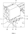
- Figure 4 is a top view of the printed circuit board 112 on which the light pipe structure 116 is mounted.
- Light emitting devices 120 are mounted on the printed circuit board 112.
- the light emitting device may be for example a light emitting diode (LED).
- the light from each of the light emitting devices is 120 coupled to a light pipe 118 (not shown) of the light pipe structure 116 mounted thereover.
- isolation slots 122 which are positioned between the light emitting devices 120.
- At least one retention feedthrough 124 is positioned behind the last light emitting device 120 and is used for mounting the light pipe structure 116 to the printed circuit board 112.
- a notch 126 on a front end of the printed circuit board 116 is also used to mount the light pipe structure 116 thereto.
- Figure 5 is a bottom view of the printed circuit board 112 on which the light pipe structure (not shown) is mounted.
- the light pipe structure 116 is mounted on the printed circuit board 112.
- a clip 130 at the front end of the light pipe structure 116 is attached at the notch 126 ( Fig. 4 ) and a retention barb 135 at a back end of the light pipe structure 116 is inserted through feedthrough 124 ( Fig. 4 ) to mount the light pipe structure on the printed circuit board 116.
- FIG 6 is a cross-sectional view of the exemplary light pipe structure 116 shown in Figure 2 .
- the light pipe structure includes a housing 140, one or more light pipes 118 and separators 150.
- the housing 140 is an enclosure within which are positioned the light pipes 118 and the separators 150.
- the housing 140 may be formed for example of an opaque plastic material.
- the one or more light pipes 118 are positioned within the housing and have an input end 125 and an output end 127.
- the input end 125 is positioned adjacent to an opening in the housing 140 to be positioned over a light emitting device 120 positioned on the printed circuit board 112 ( Fig. 4 ).
- the output end 127 is positioned abutting a lens 115 that is positioned in an aperture 114 in the faceplate 110 ( Fig. 1 ).
- the exemplary light pipes 118 depicted in Figure 6 have a curved structure. However, other structures are also contemplated such as for example linear or angled structures (not shown).
- the light pipes 118 are formed of a solid transparent or translucent material that transmits light.
- the light pipes 118 are separated one from the other with separators 150 within the housing, as shown in Figure 6 .
- the separators 150 surround the light pipes 118 such that light does not leak within the housing from one light pipe 118 to another.
- the separators may be formed of an opaque plastic material.
- the separators may have ribs 155 attached thereto to facilitate holding the light pipes in fixed positions within the housing.
- the separators 150 have tabs 137 that extend through the housing and are positioned between openings in the housing 140.
- the openings allow light emitted by the light emitting devices 120 to enter the input end 125 of the light pipes 118.
- the tabs 137 are inserted in the slots 122 ( Fig. 4 ) of the printed circuit board 112 when the light pipe structure 116 is mounted thereto.
- the tabs 137 extending through the housing 140 and into the slots 122 in the printed circuit board 112 reduces the leakage of light from the light emitting devices 120 to adjacent light pipes 118.
- the length of the tabs 137 extending through the housing 140 may be varied according to the width of the input end 125 of the one or more light pipes 118 to facilitate reducing the leakage of light from the light emitting devices 120 to adjacent light pipes 118.
- the housing 140 includes a retention barb 135 and a clip 130 which are used to facilitate mounting the light pipe structure 116 on the printed circuit board.
- the clip 130 is aligned with notch 126 ( Fig. 4 ) on the printed circuit board.
- the retention barb 135 is inserted into feedthrough 124 ( Fig. 4 ) on the printed circuit board 112.
- FIG. 7 is a perspective view of the cross-section of the light pipe structure shown in FIG. 6 .
Landscapes
- Physics & Mathematics (AREA)
- General Physics & Mathematics (AREA)
- Engineering & Computer Science (AREA)
- Theoretical Computer Science (AREA)
- Optics & Photonics (AREA)
- Microelectronics & Electronic Packaging (AREA)
- Illuminated Signs And Luminous Advertising (AREA)
- Mounting Components In General For Electric Apparatus (AREA)
- Arrangement Of Elements, Cooling, Sealing, Or The Like Of Lighting Devices (AREA)
Abstract
Description
- The disclosure generally relates to electronic devices and, more specifically, to an electronic device having a light pipe structure for illuminating logos, buttons, and/or indicator signals.
- Consumer and market preference for electronic devices such as set top boxes, computers, game consoles, DVD players, CD players, etc., is to have such devices include logos, buttons and/or indicator signals which are illuminated. Typically, these electronic devices utilize a unitary light pipe structure to illuminate lenses visible through a faceplate of the device.
- The unitary light pipe structure is a single molded part that includes a plurality of individual light pipes. Each of the plurality of light pipes is dedicated for use with a different light emitting element to illuminate one of the lenses. However, for such unitary light pipe structures, light from one light pipe can propagate, bleed or leak to an unintended adjacent light pipe in the unitary structure. This unintended illumination will be referred to as leakage.
- This light leakage may be annoying to the user because adjacent lenses which are illuminated by unintended light can provide false information and/or cause the lens at the end of the light pipe that receives the leakage to be non-uniformly illuminated.
- The present disclosure is directed toward overcoming one or more of these drawbacks.
- According to a first aspect of the disclosure, an illumination structure for an electronic device is described. The electronic device includes a housing mounted on a printed circuit board. The housing has a plurality of light pipes and at least one separator disposed therein. The at least one separator is positioned between adjacent light pipes of the plurality of light pipes.
- In another embodiment, the housing is formed of an opaque material.
- In another embodiment, the at least one separator includes a tab on a first end extending through the housing and into a slot in the printed circuit board.
- In another embodiment, the length of the tab may be varied based on a width of an input end of a respective light pipe.
- In another embodiment, the at least one separator is formed of an opaque material.
- In another embodiment, the housing includes at least one of a clip and a retention barb.
- In another embodiment, the plurality of light pipes provide illumination to an element visible from the exterior of the housing.
- In another embodiment, the plurality of light pipes are arranged to guide illumination from a light source to light lenses mounted on the housing.
- In another embodiment, the light source includes two or more light emitting devices mounted on the printed circuit board.
- In another embodiment, at least one of the plurality of light pipes has a curved structure.
- In another embodiment, a set top box includes the electronic device.
- These and other aspects, features and advantages of the present disclosure will be described or become apparent from the following detailed description of the preferred embodiments, which is to be read in connection with the accompanying drawings.
- In the drawings, wherein like reference numerals denote similar elements throughout the views:
-
FIG. 1 is a view showing a partial frontal area of a faceplate and printed circuit board of an electronic device of the present disclosure; -
FIG. 2 is a view showing an area of the circuit board ofFIG. 1 behind the faceplate depicting two exemplary light pipe structures mounted thereon; -
FIG. 3 is a perspective view of the interior of one of the two exemplary light pipe structures mounted on the printed circuit board shown inFIG. 2 ; -
FIG. 4 is a perspective top view of the printed circuit board on which the light pipe structure is mounted; -
FIG. 5 is a bottom view of the printed circuit board on which the light pipe structure is mounted; -
FIG. 6 is a cross-sectional view of an exemplary light pipe structure shown inFIG. 2 ; and -
FIG. 7 is a perspective view of the cross-section of the light pipe structure shown inFIG. 6 . - It should be understood, that the drawings are for purposes of illustrating the concepts of the disclosure and are not necessarily the only possible configuration for illustrating the disclosure.
- The present description illustrates the principles of the present disclosure. It will thus be appreciated that those skilled in the art will be able to devise various arrangements that although not explicitly described or shown herein, embody the principles of the disclosure and are included within its spirit and scope.
- All examples and conditional language recited herein are intended for instructional purposes to aid the reader in understanding the principles of the disclosure and the concepts contributed by the inventor to furthering the art, and are to be construed as being without limitation to such specifically recited examples and conditions.
- Moreover, all statements herein reciting principals, aspects, and embodiments of the disclosure, as well as specific examples thereof, are intended to encompass both structural and functional equivalents thereof. Additionally, it is intended that such equivalents include both currently known equivalents as well as equivalents developed in the future, i.e., any elements developed to perform the same function, regardless of structure.
-
Figure 1 is an illustration of a partial view of anelectronic device 100 of the present disclosure. Theelectronic device 100 may include for example a set top box, a computer, a game console, a DVD player, and a CD player. Theelectronic device 100 includes at least one printedcircuit board 112 and afaceplate 110. The faceplate includesapertures 114 therethrough that are aligned withlight pipe lenses 115 from a light pipe structure 116 (partially shown inFig. 1 ). - Referring to
Figure 2 , there is shown a view of the printedcircuit board 112 without the faceplate 110 (not shown). One or morelight pipe structures 116 are mounted on the printedcircuit board 112. As shown in exemplaryFigure 2 , there are two light pipe structures mounted adjacent to each other on an edge of printedcircuit board 112. One or morelight pipe lenses 115 are shown on one face of each of thelight pipe structures 116. Thelight pipe lenses 115 are aligned withapertures 114 in the faceplate (Fig. 1 ) when the electronic device is assembled. -
Figure 3 is a view of the interior of one of thelight pipe structures 116 mounted on the printedcircuit board 112 shown inFig. 2 . Thelight pipe structure 116 includes one or morelight pipes 118. Eachlight pipe 118 is coupled at its output to alight pipe lens 115. Alight emitting device 120 that is mounted on the printedcircuit board 112 is coupled to the input of eachlight pipe 118. -
Figure 4 is a top view of the printedcircuit board 112 on which thelight pipe structure 116 is mounted.Light emitting devices 120 are mounted on the printedcircuit board 112. The light emitting device may be for example a light emitting diode (LED). The light from each of the light emitting devices is 120 coupled to a light pipe 118 (not shown) of thelight pipe structure 116 mounted thereover. - Additionally, with reference to
Figure 4 there are shownisolation slots 122, which are positioned between thelight emitting devices 120. At least oneretention feedthrough 124 is positioned behind the lastlight emitting device 120 and is used for mounting thelight pipe structure 116 to the printedcircuit board 112. Anotch 126 on a front end of the printedcircuit board 116 is also used to mount thelight pipe structure 116 thereto. -
Figure 5 is a bottom view of the printedcircuit board 112 on which the light pipe structure (not shown) is mounted. InFigure 5 , thelight pipe structure 116 is mounted on the printedcircuit board 112. Aclip 130 at the front end of thelight pipe structure 116 is attached at the notch 126 (Fig. 4 ) and aretention barb 135 at a back end of thelight pipe structure 116 is inserted through feedthrough 124 (Fig. 4 ) to mount the light pipe structure on the printedcircuit board 116. -
Figure 6 is a cross-sectional view of the exemplarylight pipe structure 116 shown inFigure 2 . The light pipe structure includes ahousing 140, one or morelight pipes 118 andseparators 150. Thehousing 140 is an enclosure within which are positioned thelight pipes 118 and theseparators 150. Thehousing 140 may be formed for example of an opaque plastic material. - The one or more
light pipes 118 are positioned within the housing and have aninput end 125 and anoutput end 127. Theinput end 125 is positioned adjacent to an opening in thehousing 140 to be positioned over alight emitting device 120 positioned on the printed circuit board 112 (Fig. 4 ). Theoutput end 127 is positioned abutting alens 115 that is positioned in anaperture 114 in the faceplate 110 (Fig. 1 ). The exemplarylight pipes 118 depicted inFigure 6 have a curved structure. However, other structures are also contemplated such as for example linear or angled structures (not shown). Thelight pipes 118 are formed of a solid transparent or translucent material that transmits light. - The
light pipes 118 are separated one from the other withseparators 150 within the housing, as shown inFigure 6 . Theseparators 150 surround thelight pipes 118 such that light does not leak within the housing from onelight pipe 118 to another. The separators may be formed of an opaque plastic material. The separators may haveribs 155 attached thereto to facilitate holding the light pipes in fixed positions within the housing. - Referring to
Figure 6 , theseparators 150 havetabs 137 that extend through the housing and are positioned between openings in thehousing 140. The openings allow light emitted by thelight emitting devices 120 to enter theinput end 125 of thelight pipes 118. Thetabs 137 are inserted in the slots 122 (Fig. 4 ) of the printedcircuit board 112 when thelight pipe structure 116 is mounted thereto. Thetabs 137 extending through thehousing 140 and into theslots 122 in the printedcircuit board 112 reduces the leakage of light from thelight emitting devices 120 to adjacentlight pipes 118. Additionally, the length of thetabs 137 extending through thehousing 140 may be varied according to the width of theinput end 125 of the one or morelight pipes 118 to facilitate reducing the leakage of light from thelight emitting devices 120 to adjacentlight pipes 118. - The
housing 140 includes aretention barb 135 and aclip 130 which are used to facilitate mounting thelight pipe structure 116 on the printed circuit board. Theclip 130 is aligned with notch 126 (Fig. 4 ) on the printed circuit board. Theretention barb 135 is inserted into feedthrough 124 (Fig. 4 ) on the printedcircuit board 112. -
FIG. 7 is a perspective view of the cross-section of the light pipe structure shown inFIG. 6 .
Claims (11)
- An electronic device, comprising:a housing mounted on a printed circuit board,wherein the housing includes a plurality of light pipes and at least one separator, wherein the at least one separator is positioned between two light pipes of the plurality of light pipes.
- The electronic device of claim 1, wherein the housing is formed of an opaque material.
- The electronic device of claims 1 or 2, wherein the at least one separator includes a tab on a first end extending through the housing and into a slot in the printed circuit board.
- The electronic device of claim 3, wherein a length of the tab may be varied based on a width of an input end for a respective light pipe.
- The electronic device of any of claims 1-4, wherein the at least one separator is formed of an opaque material.
- The electronic device of any of claims 1-5, wherein the housing includes at least one of a clip and a retention barb.
- The electronic device of claim 1, wherein the plurality of light pipes provide illumination to an element visible from the exterior of the housing.
- The electronic device of claim 1, wherein the plurality of light pipes are arranged to guide illumination from a light source to lenses mounted on the housing.
- The electronic device of claim 8, wherein the light source comprises two or more light emitting devices mounted on the printed circuit board.
- The electronic device of any of claims 1-6, wherein at least one of the plurality of light pipes has a curved structure.
- A set top box, comprising:
an electronic device of any preceding claim.
Applications Claiming Priority (1)
| Application Number | Priority Date | Filing Date | Title |
|---|---|---|---|
| US201862623697P | 2018-01-30 | 2018-01-30 |
Publications (2)
| Publication Number | Publication Date |
|---|---|
| EP3518020A1 true EP3518020A1 (en) | 2019-07-31 |
| EP3518020B1 EP3518020B1 (en) | 2021-01-13 |
Family
ID=65411823
Family Applications (1)
| Application Number | Title | Priority Date | Filing Date |
|---|---|---|---|
| EP19305106.7A Not-in-force EP3518020B1 (en) | 2018-01-30 | 2019-01-29 | Light pipe assembly |
Country Status (2)
| Country | Link |
|---|---|
| US (1) | US10725235B2 (en) |
| EP (1) | EP3518020B1 (en) |
Families Citing this family (1)
| Publication number | Priority date | Publication date | Assignee | Title |
|---|---|---|---|---|
| US20250052943A1 (en) * | 2023-08-07 | 2025-02-13 | Arris Enterprises Llc | Flexible light shield for a light pipe |
Citations (3)
| Publication number | Priority date | Publication date | Assignee | Title |
|---|---|---|---|---|
| US5760754A (en) * | 1995-12-04 | 1998-06-02 | Motorola, Inc. | Light pipe assembly and electrical device using same |
| WO2002027697A2 (en) * | 2000-09-29 | 2002-04-04 | Ge Fanuc Automation North America, Inc. | Light pipe apparatus |
| WO2018152677A1 (en) * | 2017-02-21 | 2018-08-30 | 深圳市锐明技术股份有限公司 | Light guide apparatus and board card apparatus |
Family Cites Families (2)
| Publication number | Priority date | Publication date | Assignee | Title |
|---|---|---|---|---|
| US5327328A (en) * | 1993-05-28 | 1994-07-05 | Dialight Corporation | Lightpipe and lightpipe array for redirecting light from a surface mount led |
| US7293904B2 (en) * | 2005-09-28 | 2007-11-13 | Cisco Technology, Inc. | Light pipe insulation techniques |
-
2019
- 2019-01-29 EP EP19305106.7A patent/EP3518020B1/en not_active Not-in-force
- 2019-01-30 US US16/262,787 patent/US10725235B2/en active Active
Patent Citations (3)
| Publication number | Priority date | Publication date | Assignee | Title |
|---|---|---|---|---|
| US5760754A (en) * | 1995-12-04 | 1998-06-02 | Motorola, Inc. | Light pipe assembly and electrical device using same |
| WO2002027697A2 (en) * | 2000-09-29 | 2002-04-04 | Ge Fanuc Automation North America, Inc. | Light pipe apparatus |
| WO2018152677A1 (en) * | 2017-02-21 | 2018-08-30 | 深圳市锐明技术股份有限公司 | Light guide apparatus and board card apparatus |
Also Published As
| Publication number | Publication date |
|---|---|
| US10725235B2 (en) | 2020-07-28 |
| EP3518020B1 (en) | 2021-01-13 |
| US20190235159A1 (en) | 2019-08-01 |
Similar Documents
| Publication | Publication Date | Title |
|---|---|---|
| CN107092050B (en) | Light guide structure for guiding light emitted by a plurality of light emitting components and light emitting device | |
| US10725235B2 (en) | Light pipe assembly | |
| JP2020017566A (en) | Lighting structure of electronic equipment and LED lens | |
| CN112837708A (en) | Portable solid state hard disk module | |
| US7143467B2 (en) | Vacuum cleaner with light guiding element | |
| KR20170041564A (en) | Multimedia data transfering apparatus | |
| CN111780069A (en) | LED driver | |
| JP2001118411A (en) | Vehicle lighting | |
| KR101786952B1 (en) | Camera with illumination sub assembly | |
| US10101523B1 (en) | Light guide heat dissipation module and electronic device | |
| JP6750235B2 (en) | Display device, electronic device, and light guide unit | |
| CN109119849B (en) | Power socket device | |
| US20140168886A1 (en) | Motherboard module having air duct with indicators | |
| EP2662876A1 (en) | Vehicle interior component including indicator | |
| US20160260555A1 (en) | Compact button with illuminated graphic | |
| TWI909837B (en) | Partition and storage device using thereof | |
| CN218972502U (en) | Light guide assembly, light emitting structure and terminal equipment | |
| EP3865764A1 (en) | Luminaire | |
| TWI770526B (en) | Computer | |
| CN114025553B (en) | Electric box | |
| KR101930318B1 (en) | Terminal assembly having light source | |
| TW202437055A (en) | Light-leakage proof electronic device | |
| KR101050841B1 (en) | Electronic devices with concave and convex indicator | |
| KR100425697B1 (en) | Shelf for sorting and fixing an optical cable | |
| JP6766430B2 (en) | Communication module |
Legal Events
| Date | Code | Title | Description |
|---|---|---|---|
| PUAI | Public reference made under article 153(3) epc to a published international application that has entered the european phase |
Free format text: ORIGINAL CODE: 0009012 |
|
| STAA | Information on the status of an ep patent application or granted ep patent |
Free format text: STATUS: THE APPLICATION HAS BEEN PUBLISHED |
|
| AK | Designated contracting states |
Kind code of ref document: A1 Designated state(s): AL AT BE BG CH CY CZ DE DK EE ES FI FR GB GR HR HU IE IS IT LI LT LU LV MC MK MT NL NO PL PT RO RS SE SI SK SM TR |
|
| AX | Request for extension of the european patent |
Extension state: BA ME |
|
| STAA | Information on the status of an ep patent application or granted ep patent |
Free format text: STATUS: REQUEST FOR EXAMINATION WAS MADE |
|
| 17P | Request for examination filed |
Effective date: 20200128 |
|
| RBV | Designated contracting states (corrected) |
Designated state(s): AL AT BE BG CH CY CZ DE DK EE ES FI FR GB GR HR HU IE IS IT LI LT LU LV MC MK MT NL NO PL PT RO RS SE SI SK SM TR |
|
| GRAP | Despatch of communication of intention to grant a patent |
Free format text: ORIGINAL CODE: EPIDOSNIGR1 |
|
| STAA | Information on the status of an ep patent application or granted ep patent |
Free format text: STATUS: GRANT OF PATENT IS INTENDED |
|
| RIC1 | Information provided on ipc code assigned before grant |
Ipc: G09F 9/00 20060101ALI20200326BHEP Ipc: G02B 6/00 20060101ALI20200326BHEP Ipc: G02B 27/09 20060101ALI20200326BHEP Ipc: G09F 13/22 20060101ALI20200326BHEP Ipc: F21V 8/00 20060101ALI20200326BHEP Ipc: G09F 13/04 20060101ALI20200326BHEP Ipc: H05K 5/02 20060101ALI20200326BHEP Ipc: G02B 27/00 20060101AFI20200326BHEP Ipc: H05K 5/00 20060101ALI20200326BHEP Ipc: G09F 23/00 20060101ALI20200326BHEP |
|
| INTG | Intention to grant announced |
Effective date: 20200414 |
|
| GRAJ | Information related to disapproval of communication of intention to grant by the applicant or resumption of examination proceedings by the epo deleted |
Free format text: ORIGINAL CODE: EPIDOSDIGR1 |
|
| STAA | Information on the status of an ep patent application or granted ep patent |
Free format text: STATUS: REQUEST FOR EXAMINATION WAS MADE |
|
| INTC | Intention to grant announced (deleted) | ||
| GRAP | Despatch of communication of intention to grant a patent |
Free format text: ORIGINAL CODE: EPIDOSNIGR1 |
|
| STAA | Information on the status of an ep patent application or granted ep patent |
Free format text: STATUS: GRANT OF PATENT IS INTENDED |
|
| INTG | Intention to grant announced |
Effective date: 20200923 |
|
| GRAS | Grant fee paid |
Free format text: ORIGINAL CODE: EPIDOSNIGR3 |
|
| GRAA | (expected) grant |
Free format text: ORIGINAL CODE: 0009210 |
|
| STAA | Information on the status of an ep patent application or granted ep patent |
Free format text: STATUS: THE PATENT HAS BEEN GRANTED |
|
| AK | Designated contracting states |
Kind code of ref document: B1 Designated state(s): AL AT BE BG CH CY CZ DE DK EE ES FI FR GB GR HR HU IE IS IT LI LT LU LV MC MK MT NL NO PL PT RO RS SE SI SK SM TR |
|
| REG | Reference to a national code |
Ref country code: GB Ref legal event code: FG4D |
|
| REG | Reference to a national code |
Ref country code: CH Ref legal event code: EP |
|
| REG | Reference to a national code |
Ref country code: IE Ref legal event code: FG4D |
|
| REG | Reference to a national code |
Ref country code: DE Ref legal event code: R096 Ref document number: 602019002190 Country of ref document: DE |
|
| REG | Reference to a national code |
Ref country code: AT Ref legal event code: REF Ref document number: 1355000 Country of ref document: AT Kind code of ref document: T Effective date: 20210215 |
|
| REG | Reference to a national code |
Ref country code: AT Ref legal event code: MK05 Ref document number: 1355000 Country of ref document: AT Kind code of ref document: T Effective date: 20210113 |
|
| REG | Reference to a national code |
Ref country code: NL Ref legal event code: MP Effective date: 20210113 |
|
| REG | Reference to a national code |
Ref country code: LT Ref legal event code: MG9D |
|
| PG25 | Lapsed in a contracting state [announced via postgrant information from national office to epo] |
Ref country code: LT Free format text: LAPSE BECAUSE OF FAILURE TO SUBMIT A TRANSLATION OF THE DESCRIPTION OR TO PAY THE FEE WITHIN THE PRESCRIBED TIME-LIMIT Effective date: 20210113 Ref country code: PT Free format text: LAPSE BECAUSE OF FAILURE TO SUBMIT A TRANSLATION OF THE DESCRIPTION OR TO PAY THE FEE WITHIN THE PRESCRIBED TIME-LIMIT Effective date: 20210513 Ref country code: NO Free format text: LAPSE BECAUSE OF FAILURE TO SUBMIT A TRANSLATION OF THE DESCRIPTION OR TO PAY THE FEE WITHIN THE PRESCRIBED TIME-LIMIT Effective date: 20210413 Ref country code: FI Free format text: LAPSE BECAUSE OF FAILURE TO SUBMIT A TRANSLATION OF THE DESCRIPTION OR TO PAY THE FEE WITHIN THE PRESCRIBED TIME-LIMIT Effective date: 20210113 Ref country code: GR Free format text: LAPSE BECAUSE OF FAILURE TO SUBMIT A TRANSLATION OF THE DESCRIPTION OR TO PAY THE FEE WITHIN THE PRESCRIBED TIME-LIMIT Effective date: 20210414 Ref country code: BG Free format text: LAPSE BECAUSE OF FAILURE TO SUBMIT A TRANSLATION OF THE DESCRIPTION OR TO PAY THE FEE WITHIN THE PRESCRIBED TIME-LIMIT Effective date: 20210413 Ref country code: HR Free format text: LAPSE BECAUSE OF FAILURE TO SUBMIT A TRANSLATION OF THE DESCRIPTION OR TO PAY THE FEE WITHIN THE PRESCRIBED TIME-LIMIT Effective date: 20210113 |
|
| PG25 | Lapsed in a contracting state [announced via postgrant information from national office to epo] |
Ref country code: AT Free format text: LAPSE BECAUSE OF FAILURE TO SUBMIT A TRANSLATION OF THE DESCRIPTION OR TO PAY THE FEE WITHIN THE PRESCRIBED TIME-LIMIT Effective date: 20210113 Ref country code: LV Free format text: LAPSE BECAUSE OF FAILURE TO SUBMIT A TRANSLATION OF THE DESCRIPTION OR TO PAY THE FEE WITHIN THE PRESCRIBED TIME-LIMIT Effective date: 20210113 Ref country code: PL Free format text: LAPSE BECAUSE OF FAILURE TO SUBMIT A TRANSLATION OF THE DESCRIPTION OR TO PAY THE FEE WITHIN THE PRESCRIBED TIME-LIMIT Effective date: 20210113 Ref country code: RS Free format text: LAPSE BECAUSE OF FAILURE TO SUBMIT A TRANSLATION OF THE DESCRIPTION OR TO PAY THE FEE WITHIN THE PRESCRIBED TIME-LIMIT Effective date: 20210113 Ref country code: SE Free format text: LAPSE BECAUSE OF FAILURE TO SUBMIT A TRANSLATION OF THE DESCRIPTION OR TO PAY THE FEE WITHIN THE PRESCRIBED TIME-LIMIT Effective date: 20210113 |
|
| PG25 | Lapsed in a contracting state [announced via postgrant information from national office to epo] |
Ref country code: LU Free format text: LAPSE BECAUSE OF NON-PAYMENT OF DUE FEES Effective date: 20210129 Ref country code: IS Free format text: LAPSE BECAUSE OF FAILURE TO SUBMIT A TRANSLATION OF THE DESCRIPTION OR TO PAY THE FEE WITHIN THE PRESCRIBED TIME-LIMIT Effective date: 20210513 |
|
| REG | Reference to a national code |
Ref country code: BE Ref legal event code: MM Effective date: 20210131 |
|
| REG | Reference to a national code |
Ref country code: DE Ref legal event code: R097 Ref document number: 602019002190 Country of ref document: DE |
|
| PG25 | Lapsed in a contracting state [announced via postgrant information from national office to epo] |
Ref country code: MC Free format text: LAPSE BECAUSE OF FAILURE TO SUBMIT A TRANSLATION OF THE DESCRIPTION OR TO PAY THE FEE WITHIN THE PRESCRIBED TIME-LIMIT Effective date: 20210113 Ref country code: CZ Free format text: LAPSE BECAUSE OF FAILURE TO SUBMIT A TRANSLATION OF THE DESCRIPTION OR TO PAY THE FEE WITHIN THE PRESCRIBED TIME-LIMIT Effective date: 20210113 Ref country code: EE Free format text: LAPSE BECAUSE OF FAILURE TO SUBMIT A TRANSLATION OF THE DESCRIPTION OR TO PAY THE FEE WITHIN THE PRESCRIBED TIME-LIMIT Effective date: 20210113 Ref country code: SM Free format text: LAPSE BECAUSE OF FAILURE TO SUBMIT A TRANSLATION OF THE DESCRIPTION OR TO PAY THE FEE WITHIN THE PRESCRIBED TIME-LIMIT Effective date: 20210113 |
|
| PLBE | No opposition filed within time limit |
Free format text: ORIGINAL CODE: 0009261 |
|
| STAA | Information on the status of an ep patent application or granted ep patent |
Free format text: STATUS: NO OPPOSITION FILED WITHIN TIME LIMIT |
|
| PG25 | Lapsed in a contracting state [announced via postgrant information from national office to epo] |
Ref country code: DK Free format text: LAPSE BECAUSE OF FAILURE TO SUBMIT A TRANSLATION OF THE DESCRIPTION OR TO PAY THE FEE WITHIN THE PRESCRIBED TIME-LIMIT Effective date: 20210113 Ref country code: RO Free format text: LAPSE BECAUSE OF FAILURE TO SUBMIT A TRANSLATION OF THE DESCRIPTION OR TO PAY THE FEE WITHIN THE PRESCRIBED TIME-LIMIT Effective date: 20210113 Ref country code: SK Free format text: LAPSE BECAUSE OF FAILURE TO SUBMIT A TRANSLATION OF THE DESCRIPTION OR TO PAY THE FEE WITHIN THE PRESCRIBED TIME-LIMIT Effective date: 20210113 |
|
| 26N | No opposition filed |
Effective date: 20211014 |
|
| PG25 | Lapsed in a contracting state [announced via postgrant information from national office to epo] |
Ref country code: ES Free format text: LAPSE BECAUSE OF FAILURE TO SUBMIT A TRANSLATION OF THE DESCRIPTION OR TO PAY THE FEE WITHIN THE PRESCRIBED TIME-LIMIT Effective date: 20210113 Ref country code: AL Free format text: LAPSE BECAUSE OF FAILURE TO SUBMIT A TRANSLATION OF THE DESCRIPTION OR TO PAY THE FEE WITHIN THE PRESCRIBED TIME-LIMIT Effective date: 20210113 Ref country code: IE Free format text: LAPSE BECAUSE OF NON-PAYMENT OF DUE FEES Effective date: 20210129 |
|
| PG25 | Lapsed in a contracting state [announced via postgrant information from national office to epo] |
Ref country code: SI Free format text: LAPSE BECAUSE OF FAILURE TO SUBMIT A TRANSLATION OF THE DESCRIPTION OR TO PAY THE FEE WITHIN THE PRESCRIBED TIME-LIMIT Effective date: 20210113 |
|
| PG25 | Lapsed in a contracting state [announced via postgrant information from national office to epo] |
Ref country code: IT Free format text: LAPSE BECAUSE OF FAILURE TO SUBMIT A TRANSLATION OF THE DESCRIPTION OR TO PAY THE FEE WITHIN THE PRESCRIBED TIME-LIMIT Effective date: 20210113 |
|
| PG25 | Lapsed in a contracting state [announced via postgrant information from national office to epo] |
Ref country code: IS Free format text: LAPSE BECAUSE OF FAILURE TO SUBMIT A TRANSLATION OF THE DESCRIPTION OR TO PAY THE FEE WITHIN THE PRESCRIBED TIME-LIMIT Effective date: 20210513 |
|
| PG25 | Lapsed in a contracting state [announced via postgrant information from national office to epo] |
Ref country code: BE Free format text: LAPSE BECAUSE OF NON-PAYMENT OF DUE FEES Effective date: 20210131 |
|
| REG | Reference to a national code |
Ref country code: CH Ref legal event code: PL |
|
| PG25 | Lapsed in a contracting state [announced via postgrant information from national office to epo] |
Ref country code: LI Free format text: LAPSE BECAUSE OF NON-PAYMENT OF DUE FEES Effective date: 20220131 Ref country code: CH Free format text: LAPSE BECAUSE OF NON-PAYMENT OF DUE FEES Effective date: 20220131 |
|
| PGFP | Annual fee paid to national office [announced via postgrant information from national office to epo] |
Ref country code: FR Payment date: 20230124 Year of fee payment: 5 |
|
| PGFP | Annual fee paid to national office [announced via postgrant information from national office to epo] |
Ref country code: GB Payment date: 20230124 Year of fee payment: 5 Ref country code: DE Payment date: 20230127 Year of fee payment: 5 |
|
| P01 | Opt-out of the competence of the unified patent court (upc) registered |
Effective date: 20230514 |
|
| PG25 | Lapsed in a contracting state [announced via postgrant information from national office to epo] |
Ref country code: NL Free format text: LAPSE BECAUSE OF NON-PAYMENT OF DUE FEES Effective date: 20210113 Ref country code: CY Free format text: LAPSE BECAUSE OF FAILURE TO SUBMIT A TRANSLATION OF THE DESCRIPTION OR TO PAY THE FEE WITHIN THE PRESCRIBED TIME-LIMIT Effective date: 20210113 |
|
| PG25 | Lapsed in a contracting state [announced via postgrant information from national office to epo] |
Ref country code: HU Free format text: LAPSE BECAUSE OF FAILURE TO SUBMIT A TRANSLATION OF THE DESCRIPTION OR TO PAY THE FEE WITHIN THE PRESCRIBED TIME-LIMIT; INVALID AB INITIO Effective date: 20190129 |
|
| PG25 | Lapsed in a contracting state [announced via postgrant information from national office to epo] |
Ref country code: MK Free format text: LAPSE BECAUSE OF FAILURE TO SUBMIT A TRANSLATION OF THE DESCRIPTION OR TO PAY THE FEE WITHIN THE PRESCRIBED TIME-LIMIT Effective date: 20210113 |
|
| PG25 | Lapsed in a contracting state [announced via postgrant information from national office to epo] |
Ref country code: TR Free format text: LAPSE BECAUSE OF FAILURE TO SUBMIT A TRANSLATION OF THE DESCRIPTION OR TO PAY THE FEE WITHIN THE PRESCRIBED TIME-LIMIT Effective date: 20210113 |
|
| REG | Reference to a national code |
Ref country code: DE Ref legal event code: R119 Ref document number: 602019002190 Country of ref document: DE |
|
| GBPC | Gb: european patent ceased through non-payment of renewal fee |
Effective date: 20240129 |
|
| PG25 | Lapsed in a contracting state [announced via postgrant information from national office to epo] |
Ref country code: MT Free format text: LAPSE BECAUSE OF FAILURE TO SUBMIT A TRANSLATION OF THE DESCRIPTION OR TO PAY THE FEE WITHIN THE PRESCRIBED TIME-LIMIT Effective date: 20210113 |
|
| PG25 | Lapsed in a contracting state [announced via postgrant information from national office to epo] |
Ref country code: DE Free format text: LAPSE BECAUSE OF NON-PAYMENT OF DUE FEES Effective date: 20240801 |
|
| PG25 | Lapsed in a contracting state [announced via postgrant information from national office to epo] |
Ref country code: GB Free format text: LAPSE BECAUSE OF NON-PAYMENT OF DUE FEES Effective date: 20240129 |
|
| PG25 | Lapsed in a contracting state [announced via postgrant information from national office to epo] |
Ref country code: FR Free format text: LAPSE BECAUSE OF NON-PAYMENT OF DUE FEES Effective date: 20240131 |
|
| PG25 | Lapsed in a contracting state [announced via postgrant information from national office to epo] |
Ref country code: GB Free format text: LAPSE BECAUSE OF NON-PAYMENT OF DUE FEES Effective date: 20240129 Ref country code: FR Free format text: LAPSE BECAUSE OF NON-PAYMENT OF DUE FEES Effective date: 20240131 Ref country code: DE Free format text: LAPSE BECAUSE OF NON-PAYMENT OF DUE FEES Effective date: 20240801 |