EP3514935A1 - Forward fed boost converter for flyback switched mode power supply and method thereof - Google Patents
Forward fed boost converter for flyback switched mode power supply and method thereof Download PDFInfo
- Publication number
- EP3514935A1 EP3514935A1 EP19151126.0A EP19151126A EP3514935A1 EP 3514935 A1 EP3514935 A1 EP 3514935A1 EP 19151126 A EP19151126 A EP 19151126A EP 3514935 A1 EP3514935 A1 EP 3514935A1
- Authority
- EP
- European Patent Office
- Prior art keywords
- regulator
- primary side
- smps
- switching regulator
- controller
- Prior art date
- Legal status (The legal status is an assumption and is not a legal conclusion. Google has not performed a legal analysis and makes no representation as to the accuracy of the status listed.)
- Withdrawn
Links
Images



Classifications
-
- H—ELECTRICITY
- H02—GENERATION; CONVERSION OR DISTRIBUTION OF ELECTRIC POWER
- H02M—APPARATUS FOR CONVERSION BETWEEN AC AND AC, BETWEEN AC AND DC, OR BETWEEN DC AND DC, AND FOR USE WITH MAINS OR SIMILAR POWER SUPPLY SYSTEMS; CONVERSION OF DC OR AC INPUT POWER INTO SURGE OUTPUT POWER; CONTROL OR REGULATION THEREOF
- H02M1/00—Details of apparatus for conversion
- H02M1/08—Circuits specially adapted for the generation of control voltages for semiconductor devices incorporated in static converters
-
- H—ELECTRICITY
- H02—GENERATION; CONVERSION OR DISTRIBUTION OF ELECTRIC POWER
- H02M—APPARATUS FOR CONVERSION BETWEEN AC AND AC, BETWEEN AC AND DC, OR BETWEEN DC AND DC, AND FOR USE WITH MAINS OR SIMILAR POWER SUPPLY SYSTEMS; CONVERSION OF DC OR AC INPUT POWER INTO SURGE OUTPUT POWER; CONTROL OR REGULATION THEREOF
- H02M1/00—Details of apparatus for conversion
- H02M1/36—Means for starting or stopping converters
-
- H—ELECTRICITY
- H02—GENERATION; CONVERSION OR DISTRIBUTION OF ELECTRIC POWER
- H02M—APPARATUS FOR CONVERSION BETWEEN AC AND AC, BETWEEN AC AND DC, OR BETWEEN DC AND DC, AND FOR USE WITH MAINS OR SIMILAR POWER SUPPLY SYSTEMS; CONVERSION OF DC OR AC INPUT POWER INTO SURGE OUTPUT POWER; CONTROL OR REGULATION THEREOF
- H02M3/00—Conversion of DC power input into DC power output
- H02M3/22—Conversion of DC power input into DC power output with intermediate conversion into AC
- H02M3/24—Conversion of DC power input into DC power output with intermediate conversion into AC by static converters
- H02M3/28—Conversion of DC power input into DC power output with intermediate conversion into AC by static converters using discharge tubes with control electrode or semiconductor devices with control electrode to produce the intermediate AC
- H02M3/325—Conversion of DC power input into DC power output with intermediate conversion into AC by static converters using discharge tubes with control electrode or semiconductor devices with control electrode to produce the intermediate AC using devices of a triode or a transistor type requiring continuous application of a control signal
- H02M3/335—Conversion of DC power input into DC power output with intermediate conversion into AC by static converters using discharge tubes with control electrode or semiconductor devices with control electrode to produce the intermediate AC using devices of a triode or a transistor type requiring continuous application of a control signal using semiconductor devices only
- H02M3/33507—Conversion of DC power input into DC power output with intermediate conversion into AC by static converters using discharge tubes with control electrode or semiconductor devices with control electrode to produce the intermediate AC using devices of a triode or a transistor type requiring continuous application of a control signal using semiconductor devices only with automatic control of the output voltage or current, e.g. flyback converters
- H02M3/33523—Conversion of DC power input into DC power output with intermediate conversion into AC by static converters using discharge tubes with control electrode or semiconductor devices with control electrode to produce the intermediate AC using devices of a triode or a transistor type requiring continuous application of a control signal using semiconductor devices only with automatic control of the output voltage or current, e.g. flyback converters with galvanic isolation between input and output of both the power stage and the feedback loop
-
- H—ELECTRICITY
- H02—GENERATION; CONVERSION OR DISTRIBUTION OF ELECTRIC POWER
- H02M—APPARATUS FOR CONVERSION BETWEEN AC AND AC, BETWEEN AC AND DC, OR BETWEEN DC AND DC, AND FOR USE WITH MAINS OR SIMILAR POWER SUPPLY SYSTEMS; CONVERSION OF DC OR AC INPUT POWER INTO SURGE OUTPUT POWER; CONTROL OR REGULATION THEREOF
- H02M3/00—Conversion of DC power input into DC power output
- H02M3/22—Conversion of DC power input into DC power output with intermediate conversion into AC
- H02M3/24—Conversion of DC power input into DC power output with intermediate conversion into AC by static converters
- H02M3/28—Conversion of DC power input into DC power output with intermediate conversion into AC by static converters using discharge tubes with control electrode or semiconductor devices with control electrode to produce the intermediate AC
- H02M3/325—Conversion of DC power input into DC power output with intermediate conversion into AC by static converters using discharge tubes with control electrode or semiconductor devices with control electrode to produce the intermediate AC using devices of a triode or a transistor type requiring continuous application of a control signal
- H02M3/335—Conversion of DC power input into DC power output with intermediate conversion into AC by static converters using discharge tubes with control electrode or semiconductor devices with control electrode to produce the intermediate AC using devices of a triode or a transistor type requiring continuous application of a control signal using semiconductor devices only
- H02M3/33538—Conversion of DC power input into DC power output with intermediate conversion into AC by static converters using discharge tubes with control electrode or semiconductor devices with control electrode to produce the intermediate AC using devices of a triode or a transistor type requiring continuous application of a control signal using semiconductor devices only of the forward type
- H02M3/33546—Conversion of DC power input into DC power output with intermediate conversion into AC by static converters using discharge tubes with control electrode or semiconductor devices with control electrode to produce the intermediate AC using devices of a triode or a transistor type requiring continuous application of a control signal using semiconductor devices only of the forward type with automatic control of the output voltage or current
- H02M3/33553—Conversion of DC power input into DC power output with intermediate conversion into AC by static converters using discharge tubes with control electrode or semiconductor devices with control electrode to produce the intermediate AC using devices of a triode or a transistor type requiring continuous application of a control signal using semiconductor devices only of the forward type with automatic control of the output voltage or current with galvanic isolation between input and output of both the power stage and the feedback loop
-
- H—ELECTRICITY
- H02—GENERATION; CONVERSION OR DISTRIBUTION OF ELECTRIC POWER
- H02M—APPARATUS FOR CONVERSION BETWEEN AC AND AC, BETWEEN AC AND DC, OR BETWEEN DC AND DC, AND FOR USE WITH MAINS OR SIMILAR POWER SUPPLY SYSTEMS; CONVERSION OF DC OR AC INPUT POWER INTO SURGE OUTPUT POWER; CONTROL OR REGULATION THEREOF
- H02M3/00—Conversion of DC power input into DC power output
- H02M3/22—Conversion of DC power input into DC power output with intermediate conversion into AC
- H02M3/24—Conversion of DC power input into DC power output with intermediate conversion into AC by static converters
- H02M3/28—Conversion of DC power input into DC power output with intermediate conversion into AC by static converters using discharge tubes with control electrode or semiconductor devices with control electrode to produce the intermediate AC
- H02M3/325—Conversion of DC power input into DC power output with intermediate conversion into AC by static converters using discharge tubes with control electrode or semiconductor devices with control electrode to produce the intermediate AC using devices of a triode or a transistor type requiring continuous application of a control signal
- H02M3/335—Conversion of DC power input into DC power output with intermediate conversion into AC by static converters using discharge tubes with control electrode or semiconductor devices with control electrode to produce the intermediate AC using devices of a triode or a transistor type requiring continuous application of a control signal using semiconductor devices only
- H02M3/33569—Conversion of DC power input into DC power output with intermediate conversion into AC by static converters using discharge tubes with control electrode or semiconductor devices with control electrode to produce the intermediate AC using devices of a triode or a transistor type requiring continuous application of a control signal using semiconductor devices only having several active switching elements
- H02M3/33576—Conversion of DC power input into DC power output with intermediate conversion into AC by static converters using discharge tubes with control electrode or semiconductor devices with control electrode to produce the intermediate AC using devices of a triode or a transistor type requiring continuous application of a control signal using semiconductor devices only having several active switching elements having at least one active switching element at the secondary side of an isolation transformer
- H02M3/33592—Conversion of DC power input into DC power output with intermediate conversion into AC by static converters using discharge tubes with control electrode or semiconductor devices with control electrode to produce the intermediate AC using devices of a triode or a transistor type requiring continuous application of a control signal using semiconductor devices only having several active switching elements having at least one active switching element at the secondary side of an isolation transformer having a synchronous rectifier circuit or a synchronous freewheeling circuit at the secondary side of an isolation transformer
-
- H—ELECTRICITY
- H02—GENERATION; CONVERSION OR DISTRIBUTION OF ELECTRIC POWER
- H02M—APPARATUS FOR CONVERSION BETWEEN AC AND AC, BETWEEN AC AND DC, OR BETWEEN DC AND DC, AND FOR USE WITH MAINS OR SIMILAR POWER SUPPLY SYSTEMS; CONVERSION OF DC OR AC INPUT POWER INTO SURGE OUTPUT POWER; CONTROL OR REGULATION THEREOF
- H02M7/00—Conversion of AC power input into DC power output; Conversion of DC power input into AC power output
- H02M7/02—Conversion of AC power input into DC power output without possibility of reversal
- H02M7/04—Conversion of AC power input into DC power output without possibility of reversal by static converters
- H02M7/06—Conversion of AC power input into DC power output without possibility of reversal by static converters using discharge tubes without control electrode or semiconductor devices without control electrode
- H02M7/064—Conversion of AC power input into DC power output without possibility of reversal by static converters using discharge tubes without control electrode or semiconductor devices without control electrode with several outputs
-
- H—ELECTRICITY
- H02—GENERATION; CONVERSION OR DISTRIBUTION OF ELECTRIC POWER
- H02M—APPARATUS FOR CONVERSION BETWEEN AC AND AC, BETWEEN AC AND DC, OR BETWEEN DC AND DC, AND FOR USE WITH MAINS OR SIMILAR POWER SUPPLY SYSTEMS; CONVERSION OF DC OR AC INPUT POWER INTO SURGE OUTPUT POWER; CONTROL OR REGULATION THEREOF
- H02M7/00—Conversion of AC power input into DC power output; Conversion of DC power input into AC power output
- H02M7/02—Conversion of AC power input into DC power output without possibility of reversal
- H02M7/04—Conversion of AC power input into DC power output without possibility of reversal by static converters
- H02M7/06—Conversion of AC power input into DC power output without possibility of reversal by static converters using discharge tubes without control electrode or semiconductor devices without control electrode
- H02M7/068—Conversion of AC power input into DC power output without possibility of reversal by static converters using discharge tubes without control electrode or semiconductor devices without control electrode mounted on a transformer
-
- H—ELECTRICITY
- H02—GENERATION; CONVERSION OR DISTRIBUTION OF ELECTRIC POWER
- H02M—APPARATUS FOR CONVERSION BETWEEN AC AND AC, BETWEEN AC AND DC, OR BETWEEN DC AND DC, AND FOR USE WITH MAINS OR SIMILAR POWER SUPPLY SYSTEMS; CONVERSION OF DC OR AC INPUT POWER INTO SURGE OUTPUT POWER; CONTROL OR REGULATION THEREOF
- H02M7/00—Conversion of AC power input into DC power output; Conversion of DC power input into AC power output
- H02M7/02—Conversion of AC power input into DC power output without possibility of reversal
- H02M7/04—Conversion of AC power input into DC power output without possibility of reversal by static converters
- H02M7/12—Conversion of AC power input into DC power output without possibility of reversal by static converters using discharge tubes with control electrode or semiconductor devices with control electrode
- H02M7/21—Conversion of AC power input into DC power output without possibility of reversal by static converters using discharge tubes with control electrode or semiconductor devices with control electrode using devices of a triode or transistor type requiring continuous application of a control signal
- H02M7/217—Conversion of AC power input into DC power output without possibility of reversal by static converters using discharge tubes with control electrode or semiconductor devices with control electrode using devices of a triode or transistor type requiring continuous application of a control signal using semiconductor devices only
- H02M7/219—Conversion of AC power input into DC power output without possibility of reversal by static converters using discharge tubes with control electrode or semiconductor devices with control electrode using devices of a triode or transistor type requiring continuous application of a control signal using semiconductor devices only in a bridge configuration
-
- H—ELECTRICITY
- H02—GENERATION; CONVERSION OR DISTRIBUTION OF ELECTRIC POWER
- H02M—APPARATUS FOR CONVERSION BETWEEN AC AND AC, BETWEEN AC AND DC, OR BETWEEN DC AND DC, AND FOR USE WITH MAINS OR SIMILAR POWER SUPPLY SYSTEMS; CONVERSION OF DC OR AC INPUT POWER INTO SURGE OUTPUT POWER; CONTROL OR REGULATION THEREOF
- H02M1/00—Details of apparatus for conversion
- H02M1/0003—Details of control, feedback or regulation circuits
- H02M1/0006—Arrangements for supplying an adequate voltage to the control circuit of converters
-
- H—ELECTRICITY
- H02—GENERATION; CONVERSION OR DISTRIBUTION OF ELECTRIC POWER
- H02M—APPARATUS FOR CONVERSION BETWEEN AC AND AC, BETWEEN AC AND DC, OR BETWEEN DC AND DC, AND FOR USE WITH MAINS OR SIMILAR POWER SUPPLY SYSTEMS; CONVERSION OF DC OR AC INPUT POWER INTO SURGE OUTPUT POWER; CONTROL OR REGULATION THEREOF
- H02M1/00—Details of apparatus for conversion
- H02M1/0048—Circuits or arrangements for reducing losses
- H02M1/0054—Transistor switching losses
-
- Y—GENERAL TAGGING OF NEW TECHNOLOGICAL DEVELOPMENTS; GENERAL TAGGING OF CROSS-SECTIONAL TECHNOLOGIES SPANNING OVER SEVERAL SECTIONS OF THE IPC; TECHNICAL SUBJECTS COVERED BY FORMER USPC CROSS-REFERENCE ART COLLECTIONS [XRACs] AND DIGESTS
- Y02—TECHNOLOGIES OR APPLICATIONS FOR MITIGATION OR ADAPTATION AGAINST CLIMATE CHANGE
- Y02B—CLIMATE CHANGE MITIGATION TECHNOLOGIES RELATED TO BUILDINGS, e.g. HOUSING, HOUSE APPLIANCES OR RELATED END-USER APPLICATIONS
- Y02B70/00—Technologies for an efficient end-user side electric power management and consumption
- Y02B70/10—Technologies improving the efficiency by using switched-mode power supplies [SMPS], i.e. efficient power electronics conversion e.g. power factor correction or reduction of losses in power supplies or efficient standby modes
Definitions
- This disclosure relates generally to switched mode power supply (“SMPS”), and more specifically, but not exclusively, to a forward fed boost converter for flyback SMPS.
- SMPS switched mode power supply
- SMPS is a known electronic power supply which uses switching regulators to convert electricity as efficiently as possible.
- Embodiments address the need to create a forward fed boost converter for flyback SMPS.
- a flyback type switched mode power supply including a primary side controller on a primary side, a first switch on the primary side and a transformer including a primary side winding on the primary side, a secondary side winding on a secondary side, and an auxiliary winding on the primary side connected to a first switching regulator, wherein the first switching regulator is supplied during a primary stroke from the auxiliary winding when the first switch is on.
- the flyback SMPS further including the transformer, including a secondary auxiliary winding on the secondary side connected to a second switching regulator, wherein the second switching regulator is supplied during a primary stroke from the secondary auxiliary winding.
- the flyback type SMPS further including a startup resistor on the primary side connected to the first switching regulator.
- the flyback type SMPS further including second switch on the secondary side which is driven by the second switching regulator with an integrated synchronous rectifier controller.
- the first switching regulator and the second switching regulator are a boost type regulator.
- the boost type regulator includes a pulse width modulator regulator, a switch, a rectifying diode, an inductor, and an output capacitor.
- the PWM regulator is configured to regulate an internal working voltage of the boost type regulator to a fixed voltage which is greater than or equal to an input voltage of the boost type regulator.
- the source of the switch of the boost type regulator is grounded.
- Various embodiments described herein relate to a method for supplying a controller using a flyback type switched mode power supply, the SMPS including a primary side controller on a primary side, a first switch on the primary side, a transformer including a primary side winding on the primary side, a secondary side winding on a secondary side and an auxiliary winding on the primary side connected to a first switching regulator, the method including the steps of turning on the first switch and supplying the first switching regulator during a primary stroke from an auxiliary winding.
- the method for supplying a controller using a flyback type SMPS including the transformer, including a secondary auxiliary winding on the secondary side connected to a second switching regulator, the method further including supplying the second switching regulator during a primary stroke from the secondary auxiliary winding.
- the method for supplying a controller using a flyback type SMPS further including connecting a startup resistor on the primary side to the first switching regulator.
- the method for supplying a controller using a flyback type SMPS further including driving a second switch on the secondary side by the second switching regulator with an integrated synchronous rectifier controller.
- the first switching regulator and the second switching regulator are a boost type regulator.
- the boost type regulator includes a pulse width modulator regulator, a switch, a rectifying diode, an inductor, and an output capacitor.
- the PWM regulator is configured to regulate an internal working voltage of the boost type regulator to a fixed voltage which is greater than or equal to an input voltage of the boost type regulator.
- the source of the switch of the boost type regulator is grounded.
- An isolated flyback SMPS for a smart charging application includes alternating current (“AC") mains power on the primary side which supplies the circuit.
- the AC mains are connected by bridge rectifier diodes to an input capacitor.
- the primary side of the circuit includes an SMPS controller IC which drives a MOSFET switch and via a transformer, the energy is transferred to an output capacitor.
- the output voltage is controlled by a controller IC on the secondary side via a signal transformer.
- the output voltage setting is typically set by the smart phone or tablet by USB connections.
- the input side and the output side are electrically isolated by both transformers on the primary side and the secondary side of the circuit.
- the controller IC on the primary side is supplied by the auxiliary winding of the transformer.
- the internal working voltage of the controller IC on the primary side is generated by the internal series regulator.
- FIG. 1 illustrates a timing diagram 100 for a flyback SMPS for smart charging applications.
- the timing diagram 100 includes separate timing diagrams for gate1 101, drain1 102 and auxiliary 103.
- the input switch is switched on and when it is switched on energy is stored in transformer T1 during the primary stroke 104.
- the energy is released to the secondary side by a rectifier diode. Further, during the secondary stroke 105, energy is also fed into a V cc capacitor by the auxiliary winding with a rectifier diode.
- N a is defined as the number of turns of the primary transformer winding.
- N a is defined as the number of turns of the auxiliary transformer winding.
- V in is defined as the input voltage.
- N s is defined as the number of turns of the secondary transformer winding.
- V out is defined as the output voltage.
- V diode6 is defined as the forward voltage of diode D6.
- the auxiliary transformer winding voltage during the secondary stroke 105 is used to supply the primary side controller IC. Therefore the voltage of the V cc capacitor is equal to N a /N s *(V out +V diode6 )-V diode5 in which V diode5 is defined as the forward voltage of diode D5.
- a USB type C smart charger adapter supports an approximate output voltage range of between 3V to 20V.
- V cc voltage is much higher than required, and most of the energy to power the primary side controller IC is dissipated in the required internal series regulator.
- V cc voltage will increase at higher output loads because the peak of the high frequency ringing voltage 108 on the auxiliary winding 103 which will charge the V cc capacitor to an even higher voltage.
- the high frequency ringing voltage 108 is caused by the leakage inductance of the transformer.
- the power for the primary side supply is low (only up to approximately 2% of the output power), but, this dissipation in the primary side controller IC can become too high to keep the primary side controller IC below its maximum operating temperature.
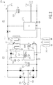
- FIG. 2 illustrates a circuit diagram 200 for a flyback SMPS for charging applications with forward supply of the primary side.
- An isolated flyback SMPS for a smart charging application includes alternating current ("AC") mains power 202 on the primary side 203 which supplies the circuit 200.
- the AC mains 202 are connected by bridge rectifier diodes 205 to an input capacitor 206.
- the primary side 203 includes a primary side controller IC 207 which drives a MOSFET switch 208 and via a transformer 209, the energy is transferred to an output capacitor 210.
- the output voltage 211 is controlled by a secondary side controller IC 212 on the secondary side 204 via a signal transformer 213.
- the output voltage 211 setting is typically set by the smart phone or tablet by USB connections 214.
- the input side and the output side are electrically isolated by transformers 209 on the primary side 203 and by transformer 213 on the secondary side 204.
- the primary side controller IC 207 on the primary side 203 is supplied by the auxiliary winding 201 of the transformer 209.
- the internal working voltage of the IC 207 on the primary side 203 is generated by the internal series regulator 215.
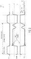
- FIG. 3 illustrates a timing diagram 300 for the flyback SMPS for charging applications with forward supply of the primary side of FIG. 2 .
- V cc voltage is now equal to equation 301 which is defined as N a / N p * V in - V diode5 .
- the input voltage range is approximately 85Vac to 264Vac. Therefore, the rectified mains peak voltage is equal to ⁇ 2*85 to ⁇ 2*264 which is approximately 120V to 373V.
- the universal mains input adapter During operation of the universal mains input adapter, there will be a 120Hz ripple (with 60Hz mains) on the capacitor on the primary side. During maximum load conditions, the lowest voltage on the capacitor on the primary side may be approximately 70V.
- a SMPS may be used to generate the internal working voltage, meaning that linear regulator is replaced by a switching regulator.
- the switching regulator may be a buck topology or a boost topology.
- Other topologies, like buck-boost, switched capacitor or any other topologies may also be possible.
- FIG. 4 illustrates a circuit diagram 400 of the current embodiment for smart charger applications with a buck type SMPS for the primary side supply.
- a buck type switching regulator is integrated in the primary side controller IC 401 of the primary side 402.
- the buck type switching regulator includes a PWM regulator 404, a switch 405, a rectifying diode 406, an inductor 407, and an output capacitor 408.
- the PWM regulator 404 regulates V int 409 to a voltage which is lower or equal to the input voltage V cc 410.
- the V int 409 voltage can be a fixed voltage or can be dependent on the operational condition.
- the driving voltage for switch 411 and gate1 412 may be lower because the peak current through switch 411 is lower at low loads. Therefore, at low loads, V int 409 may be regulated to a lower voltage.
- a boost type SMPS is advantageous over buck type SMPS.
- boost type SMPS only requires one additional IC pin (i.e., pin SW).
- the buck type SMPS requires both one additional IC pin and an additional V cc pin on the IC.
- a low pin count is advantageous for SMPS.
- boost type over buck type is that the maximum internal IC voltage is equal to V int + V diode7 (see FIG. 4 ). Because the maximum voltage for small feature size IC processes is limited, the maximum internal IC voltage being equal is advantageous.
- boost type over buck type is that switch S2 (see FIG. 6 ) is ground connected and is therefore easier to drive as compared to switch S2 405 (see FIG. 4 ) which is connected to V cc which is a high voltage.
- the losses for the primary side supply are reduced by a factor of approximately three. Furthermore, the maximum voltage on the IC is reduced from 88V to 10.7V
- the total efficiency of the smart charger improves and the dissipation in the primary side IC is reduced significantly allowing a more high-power density charger and a smaller primary side IC package.
- FIG. 5 illustrates a circuit diagram 500 of a smart charger application with a start-up resistor.
- FIG. 5 is a circuit diagram 500 which includes a start-up resistor R2 501. If no high voltage start-up circuit is present inside the IC, the start-up is performed with an external (high ohm) resistor.
- a high voltage start-up circuit allows for fast start-up and low standby power of the charger, however, requires a high voltage IC process, which adds a cost and therefore, a high voltage process is not preferred.
- V cc 502 is charged to a start-up voltage several volts above the minimum supply voltage. (e.g., V cc 502 is charged to 15V if the minimum supply voltage is 10V).
- V out 503 is initially zero, so the voltage N a / N s * (V out + V diode6 )-V diode5 will be approximately zero.
- V cc 502 is initially not supplied from the auxiliary winding 504. Only when the V out 503 reaches a minimum level, then V cc 502 supply is taken over by the auxiliary winding 504.
- the Vcc capacitor, C Vcc 505 needs to be several micro farads to supply the V cc 502 for the time during which V out 503 has not reached its minimum level.
- V cc capacitor, C Vcc 505 is several micro farads and the start-up resistor R2 501 is approximately several mega-ohms, it may take up to a second before the V cc 502 voltage has reached its start-up voltage of 15V. Therefore, after the smart charger is plugged into the mains, it may take up to a second before the smart charger starts begins to operate.
- FIG. 6 illustrates a circuit diagram 600 of the current embodiment for smart charger applications with a start-up resistor and a primary stroke supply with a boost type SMPS.
- the supply from the auxiliary winding 603 takes over the supply at the first switching cycle.
- C Vcc 604 is charged to N a / N p * V in - V diode5 .
- the C Vint 605 capacitor may be a small value (e.g., 100nF). Because of the low value of capacitor C Vint 605, the start-up after plugging the smart charger into the AC mains 606 occurs nearly immediately. (i.e. less than 100 milliseconds).
- R2 607 may also be a larger value. (e.g., 20 mega-ohms instead of 2 mega-ohms). The larger value for R2 607 may lower the losses during standby operation of the smart charger.
- FIG. 7 illustrates a circuit diagram 700 of the current embodiment with a primary stroke supply with boost type SMPS on the primary side and the secondary side.
- an additional secondary auxiliary winding 701 is included and a boost converter which includes a PWMregSec 702, inductor L2 703, switch S3 704 and diode D9 705 is included on the secondary side 706.
- a boost converter which includes a PWMregSec 702, inductor L2 703, switch S3 704 and diode D9 705 is included on the secondary side 706.
- the secondary side 706 supplies from V int Sec 707.
- the V out 708 connection is used to measure and control the output voltage, V out 708. Because the maximum output voltage on the secondary side 706 is lower than the maximum output voltage on the primary side 709, the efficiency advantage is less than for the primary side.
- FIG. 8 illustrates a circuit diagram 800 of the current embodiment for smart charger application with primary stroke supply with a boost type SMPS on the primary side and the secondary side with synchronous rectification.
- the rectifier diode D6 710 (see FIG. 7 , not shown in FIG. 8 ) is replaced by a synchronous rectifier switch S4 801.
- Switch S4 801 is driven by the secondary side controller IC, IC2 802, with an integrated synchronous rectifier controller, SRctrl 803.
- V int Sec 805 may be regulated to a voltage for driving switch S4 801 to a lowest on-state resistance.
- the gate4 804 may be driven with an optimal voltage when the boost converter from the current embodiment is added. Without the boost converter, an integrated linear regulator is needed to lower the 20V output voltage to a voltage to drive switch S4 801. (e.g., 5V to 8V).
- the integrated linear regulator would increase power dissipated in IC2 802 and with the boost regulator, the V int Sec 805 voltage may be regulated to a constant voltage for driving the synchronous rectifier switch S4 801, independent of the output voltage V out 806.
- the losses inside the primary side and secondary side IC controllers are approximately a factor of six lower, the maximum IC voltages are a factor of eight lower and standby power losses are a factor of two lower. Further, the total efficiency of the smart charger may be improved up to approximately 0.15%.
- various exemplary embodiments of the invention may be implemented in hardware.
- various exemplary embodiments may be implemented as instructions stored on a non-transitory machine-readable storage medium, such as a volatile or non-volatile memory, which may be read and executed by at least one processor to perform the operations described in detail herein.
- a non-transitory machine-readable storage medium may include any mechanism for storing information in a form readable by a machine, such as a personal or laptop computer, a server, or other computing device.
- a non-transitory machine-readable storage medium may include read-only memory (ROM), random-access memory (RAM), magnetic disk storage media, optical storage media, flash-memory devices, and similar storage media and excludes transitory signals.
- any block diagrams herein represent conceptual views of illustrative circuitry embodying the principles of the invention.
- any flow charts, flow diagrams, state transition diagrams, pseudo code, and the like represent various processes which may be substantially represented in machine readable media and so executed by a computer or processor, whether or not such computer or processor is explicitly shown.
Landscapes
- Engineering & Computer Science (AREA)
- Power Engineering (AREA)
- Dc-Dc Converters (AREA)
Abstract
Description
- This disclosure relates generally to switched mode power supply ("SMPS"), and more specifically, but not exclusively, to a forward fed boost converter for flyback SMPS.
- SMPS is a known electronic power supply which uses switching regulators to convert electricity as efficiently as possible.
- Therefore, in order to optimize the efficiency of SMPS, it is advantageous to supply the controller's integrated circuit ("IC") from a low voltage.
- When supplying the controller's IC with a high voltage, an internal series regulator is required, which results in increased losses. Further, with an internal series regulator, dissipation inside the IC can become high.
- A brief summary of various embodiments is presented below. Embodiments address the need to create a forward fed boost converter for flyback SMPS.
- In order to overcome these and other shortcomings of the prior art and in light of the need to create a forward fed boost mode converter for flyback SMPS, a brief summary of various exemplary embodiments is presented. Some simplifications and omissions may be made in the following summary, which is intended to highlight and introduce some aspects of the various exemplary embodiments, but not to limit the scope of the invention.
- Detailed descriptions of a preferred exemplary embodiment adequate to allow those of ordinary skill in the art to make and use the inventive concepts will follow in later sections.
- Various embodiments described herein relate to a flyback type switched mode power supply including a primary side controller on a primary side, a first switch on the primary side and a transformer including a primary side winding on the primary side, a secondary side winding on a secondary side, and an auxiliary winding on the primary side connected to a first switching regulator, wherein the first switching regulator is supplied during a primary stroke from the auxiliary winding when the first switch is on.
- In an embodiment of the present disclosure, the flyback SMPS, further including the transformer, including a secondary auxiliary winding on the secondary side connected to a second switching regulator, wherein the second switching regulator is supplied during a primary stroke from the secondary auxiliary winding.
- In an embodiment of the present disclosure, the flyback type SMPS, further including a startup resistor on the primary side connected to the first switching regulator.
- In an embodiment of the present disclosure, the flyback type SMPS, further including second switch on the secondary side which is driven by the second switching regulator with an integrated synchronous rectifier controller.
- In an embodiment of the present disclosure, the first switching regulator and the second switching regulator are a boost type regulator.
- In an embodiment of the present disclosure, the boost type regulator includes a pulse width modulator regulator, a switch, a rectifying diode, an inductor, and an output capacitor.
- In an embodiment of the present disclosure, the PWM regulator is configured to regulate an internal working voltage of the boost type regulator to a fixed voltage which is greater than or equal to an input voltage of the boost type regulator.
- In an embodiment of the present disclosure, the source of the switch of the boost type regulator is grounded.
- Various embodiments described herein relate to a method for supplying a controller using a flyback type switched mode power supply, the SMPS including a primary side controller on a primary side, a first switch on the primary side, a transformer including a primary side winding on the primary side, a secondary side winding on a secondary side and an auxiliary winding on the primary side connected to a first switching regulator, the method including the steps of turning on the first switch and supplying the first switching regulator during a primary stroke from an auxiliary winding.
- In an embodiment of the present disclosure, the method for supplying a controller using a flyback type SMPS, the SMPS including the transformer, including a secondary auxiliary winding on the secondary side connected to a second switching regulator, the method further including supplying the second switching regulator during a primary stroke from the secondary auxiliary winding.
- In an embodiment of the present disclosure, the method for supplying a controller using a flyback type SMPS, further including connecting a startup resistor on the primary side to the first switching regulator.
- In an embodiment of the present disclosure, the method for supplying a controller using a flyback type SMPS, further including driving a second switch on the secondary side by the second switching regulator with an integrated synchronous rectifier controller.
- In an embodiment of the present disclosure, the first switching regulator and the second switching regulator are a boost type regulator.
- In an embodiment of the present disclosure, the boost type regulator includes a pulse width modulator regulator, a switch, a rectifying diode, an inductor, and an output capacitor.
- In an embodiment of the present disclosure, the PWM regulator is configured to regulate an internal working voltage of the boost type regulator to a fixed voltage which is greater than or equal to an input voltage of the boost type regulator.
- In an embodiment of the present disclosure, the source of the switch of the boost type regulator is grounded.
- The accompanying figures, where like reference numerals refer to identical or functionally similar elements throughout the separate views, together with the detailed description below, are incorporated in and form part of the specification, and serve to further illustrate embodiments of concepts that include the claimed invention, and explain various principles and advantages of those embodiments.
- These and other more detailed and specific features are more fully disclosed in the following specification, reference being had to the accompanying drawings, in which:
-
FIG. 1 illustrates a timing diagram for a flyback SMPS for smart charging applications; -
FIG. 2 illustrates a circuit diagram for a flyback SMPS for charging applications with forward supply of the primary side; -
FIG. 3 illustrates a timing diagram for the flyback SMPS for charging applications with forward supply of the primary side ofFIG. 2 ; -
FIG. 4 illustrates a circuit diagram of the current embodiment for smart charger applications with a buck type SMPS for the primary side supply; -
FIG. 5 illustrates a circuit diagram of a smart charger application with a start-up resistor; -
FIG. 6 illustrates a circuit diagram of the current embodiment for smart charger applications with a start-up resistor and a primary stroke supply with a boost type SMPS; -
FIG. 7 illustrates a circuit diagram of the current embodiment with a primary stroke supply with boost type SMPS on the primary side and the secondary side; and -
FIG. 8 illustrates a circuit diagram of the current embodiment for smart charger application with primary stroke supply with a boost type SMPS on the primary side and the secondary side with synchronous rectification. - It should be understood that the figures are merely schematic and are not drawn to scale. It should also be understood that the same reference numerals are used throughout the figures to indicate the same or similar parts.
- The descriptions and drawings illustrate the principles of various example embodiments. It will thus be appreciated that those skilled in the art will be able to devise various arrangements that, although not explicitly described or shown herein, embody the principles of the invention and are included within its scope. Furthermore, all examples recited herein are principally intended expressly to be for pedagogical purposes to aid the reader in understanding the principles of the invention and the concepts contributed by the inventor(s) to furthering the art, and are to be construed as being without limitation to such specifically recited examples and conditions. Additionally, the term, "or," as used herein, refers to a non-exclusive or (i.e., and/or), unless otherwise indicated (e.g., "or else" or "or in the alternative"). Also, the various embodiments described herein are not necessarily mutually exclusive, as some embodiments can be combined with one or more other embodiments to form new embodiments. Descriptors such as "first," "second," "third," etc., are not meant to limit the order of elements discussed, are used to distinguish one element from the next, and are generally interchangeable.
- An isolated flyback SMPS for a smart charging application includes alternating current ("AC") mains power on the primary side which supplies the circuit. The AC mains are connected by bridge rectifier diodes to an input capacitor.
- The primary side of the circuit includes an SMPS controller IC which drives a MOSFET switch and via a transformer, the energy is transferred to an output capacitor.
- The output voltage is controlled by a controller IC on the secondary side via a signal transformer. The output voltage setting is typically set by the smart phone or tablet by USB connections.
- The input side and the output side are electrically isolated by both transformers on the primary side and the secondary side of the circuit.
- The controller IC on the primary side is supplied by the auxiliary winding of the transformer.
- The internal working voltage of the controller IC on the primary side is generated by the internal series regulator.
-
FIG. 1 illustrates a timing diagram 100 for a flyback SMPS for smart charging applications. - The timing diagram 100 includes separate timing diagrams for
gate1 101,drain1 102 and auxiliary 103. - In the flyback converter, the input switch is switched on and when it is switched on energy is stored in transformer T1 during the
primary stroke 104. - During the
secondary stroke 105, the energy is released to the secondary side by a rectifier diode. Further, during thesecondary stroke 105, energy is also fed into a Vcc capacitor by the auxiliary winding with a rectifier diode. - The voltage across the
auxiliary winding 103 during theprimary stroke 104 is equal toequation 106 which is: Na / Np * Vin. Np is defined as the number of turns of the primary transformer winding. Na is defined as the number of turns of the auxiliary transformer winding. Vin is defined as the input voltage. - The voltage across the auxiliary transformer winding 103 during the
secondary stroke 105 is equal toequation 107 which is: Na / Ns * (Vout + Vdiode6). Ns is defined as the number of turns of the secondary transformer winding. Vout is defined as the output voltage. Vdiode6 is defined as the forward voltage of diode D6. - The auxiliary transformer winding voltage during the
secondary stroke 105 is used to supply the primary side controller IC. Therefore the voltage of the Vcc capacitor is equal to Na/Ns*(Vout+Vdiode6)-Vdiode5 in which Vdiode5 is defined as the forward voltage of diode D5. - Since Vcc = Na / Ns * (Vout + Vdiode6) - Vdiode5, a change in the output voltage will also change the Vcc voltage. For the minimum output voltage setting, Vcc must be high enough to supply the primary side controller IC. For the maximum output voltage setting, Vcc will become much higher than needed, resulting in additional losses inside the controller IC.
- For example, a USB type C smart charger adapter supports an approximate output voltage range of between 3V to 20V.
- If the minimum Vcc voltage for the primary side controller IC and for the diode D5 is 10V, then the forward voltage of diode D6 is 0.7V then Na/Ns = (10 + 0.7)/(3 + 0.7) = 2.89.
- At Vout = 20V, Vcc= Na / Ns * (Vout + Vdiode6) - Vdiode5 = 59V.
- Therefore, the Vcc voltage is much higher than required, and most of the energy to power the primary side controller IC is dissipated in the required internal series regulator.
- If the internal series regulator regulates to the minimum required voltage of 10V, then at Vout = 20V, approximately 83% of the energy supplying the primary side controller IC is dissipated in the internal series regulator. Furthermore, the Vcc voltage will increase at higher output loads because the peak of the high
frequency ringing voltage 108 on the auxiliary winding 103 which will charge the Vcc capacitor to an even higher voltage. - The high
frequency ringing voltage 108 is caused by the leakage inductance of the transformer. The Vcc voltage can rise up to an additional 50%. Therefore, the highest Vcc voltage may be 59V + 50% = 88V. - In normal operation, the power for the primary side supply is low (only up to approximately 2% of the output power), but, this dissipation in the primary side controller IC can become too high to keep the primary side controller IC below its maximum operating temperature.
- Further, in high power density chargers, with a total efficiency from input to output of over 90%, approximately 2% loss is significant (i.e., 90% efficiency means 10% losses. 2% loss to power the primary side IC is a significant part of the 10%). Therefore, to limit the Vcc supply voltage range, it is advantageous to not supply to the primary side IC during the secondary stroke, but during the primary stroke (i.e., forward fed).
-
FIG. 2 illustrates a circuit diagram 200 for a flyback SMPS for charging applications with forward supply of the primary side. - An isolated flyback SMPS for a smart charging application includes alternating current ("AC")
mains power 202 on theprimary side 203 which supplies thecircuit 200. TheAC mains 202 are connected bybridge rectifier diodes 205 to aninput capacitor 206. - The
primary side 203 includes a primaryside controller IC 207 which drives aMOSFET switch 208 and via atransformer 209, the energy is transferred to anoutput capacitor 210. Theoutput voltage 211 is controlled by a secondaryside controller IC 212 on thesecondary side 204 via asignal transformer 213. Theoutput voltage 211 setting is typically set by the smart phone or tablet byUSB connections 214. - The input side and the output side are electrically isolated by
transformers 209 on theprimary side 203 and bytransformer 213 on thesecondary side 204. The primaryside controller IC 207 on theprimary side 203 is supplied by the auxiliary winding 201 of thetransformer 209. - The internal working voltage of the
IC 207 on theprimary side 203 is generated by theinternal series regulator 215. - In
FIG 2 , the polarity of the auxiliary winding 215 is reversed. -
FIG. 3 illustrates a timing diagram 300 for the flyback SMPS for charging applications with forward supply of the primary side ofFIG. 2 . - The Vcc voltage is now equal to
equation 301 which is defined as Na / Np * Vin - Vdiode5. - For a universal mains input adapter, the input voltage range is approximately 85Vac to 264Vac. Therefore, the rectified mains peak voltage is equal to √2*85 to √2*264 which is approximately 120V to 373V.
- During operation of the universal mains input adapter, there will be a 120Hz ripple (with 60Hz mains) on the capacitor on the primary side. During maximum load conditions, the lowest voltage on the capacitor on the primary side may be approximately 70V.
- For a minimum of 10V for Vcc, Na / Np is calculated at the lowest input voltage (10 + 0.7) / 70 = 0.15. For the maximum input voltage: Vcc = Na / Np* Vin - Vdiode5 = 56V.
- If the primary stroke supply is used, there is approximately no effect of peak rectification. The losses in the internal series regulator will be lower as the maximum voltage has dropped from 88V to 56V.
- To lower the losses of the supply regulator, a SMPS may be used to generate the internal working voltage, meaning that linear regulator is replaced by a switching regulator. The switching regulator may be a buck topology or a boost topology. Other topologies, like buck-boost, switched capacitor or any other topologies may also be possible.
-
FIG. 4 illustrates a circuit diagram 400 of the current embodiment for smart charger applications with a buck type SMPS for the primary side supply. - A buck type switching regulator is integrated in the primary
side controller IC 401 of theprimary side 402. - The buck type switching regulator includes a
PWM regulator 404, aswitch 405, a rectifyingdiode 406, aninductor 407, and anoutput capacitor 408. - The
PWM regulator 404 regulatesV int 409 to a voltage which is lower or equal to theinput voltage V cc 410. TheV int 409 voltage can be a fixed voltage or can be dependent on the operational condition. At low loads, the driving voltage forswitch 411 and gate1 412 may be lower because the peak current throughswitch 411 is lower at low loads. Therefore, at low loads,V int 409 may be regulated to a lower voltage. - In the current embodiment, a boost type SMPS is advantageous over buck type SMPS.
- An example of this advantage of boost type over buck type is that the boost type SMPS only requires one additional IC pin (i.e., pin SW). In contrast, the buck type SMPS requires both one additional IC pin and an additional Vcc pin on the IC. A low pin count is advantageous for SMPS.
- Another example of this advantage of boost type over buck type is that the maximum internal IC voltage is equal to Vint + Vdiode7 (see
FIG. 4 ). Because the maximum voltage for small feature size IC processes is limited, the maximum internal IC voltage being equal is advantageous. - For the buck type SMPS, for example, Vcc must be at least the minimum required Vint voltage. Therefore, if 10V minimum is needed, the maximum Vcc will be 56V, if Vcc is supplied during the primary stroke at Vin = 373V.
- For the boost type SMPS, for example, the maximum Vcc voltage is Vint + Vdiode7 = 10.7V. Therefore, for Vcc = Na / Np * Vin - Vdiode5 = 10.7V at Vin = 373V then Na/Np = 0.03. The minimum Vcc voltage will be Vcc = Na / Np * Vin - Vdiode5 = 1.4V at Vin = 70V. Therefore, for the boost type SMPS, from a 70V to 373V Vin voltage, a Vcc voltage between 1.4V and 10.7V is created and a fixed Vint voltage of 10V is created, which is suitable for high density IC processes.
- Another example of this advantage of boost type over buck type is that switch S2 (see
FIG. 6 ) is ground connected and is therefore easier to drive as compared to switch S2 405 (seeFIG. 4 ) which is connected to Vcc which is a high voltage. - As illustrated, by using the current embodiment, the losses for the primary side supply are reduced by a factor of approximately three. Furthermore, the maximum voltage on the IC is reduced from 88V to 10.7V
- The total efficiency of the smart charger improves and the dissipation in the primary side IC is reduced significantly allowing a more high-power density charger and a smaller primary side IC package.
-
FIG. 5 illustrates a circuit diagram 500 of a smart charger application with a start-up resistor. -
FIG. 5 is a circuit diagram 500 which includes a start-upresistor R2 501. If no high voltage start-up circuit is present inside the IC, the start-up is performed with an external (high ohm) resistor. - A high voltage start-up circuit allows for fast start-up and low standby power of the charger, however, requires a high voltage IC process, which adds a cost and therefore, a high voltage process is not preferred.
- To initially start-up the primary side IC,
V cc 502 is charged to a start-up voltage several volts above the minimum supply voltage. (e.g.,V cc 502 is charged to 15V if the minimum supply voltage is 10V). When the smart charger starts switching,V out 503 is initially zero, so the voltage Na / Ns * (Vout + Vdiode6)-Vdiode5 will be approximately zero. - Therefore,
V cc 502 is initially not supplied from the auxiliary winding 504. Only when theV out 503 reaches a minimum level, thenV cc 502 supply is taken over by the auxiliary winding 504. - Until
V out 503 has risen to the minimum level, the supply current is drawn from theV cc 502capacitor C Vcc 505. The Vcc capacitor,C Vcc 505 needs to be several micro farads to supply theV cc 502 for the time during whichV out 503 has not reached its minimum level. To charge theoutput capacitor C2 506 to the minimum output voltage level, when the charger is starting, is approximately several milliseconds. - When the Vcc capacitor,
C Vcc 505 is several micro farads and the start-upresistor R2 501 is approximately several mega-ohms, it may take up to a second before theV cc 502 voltage has reached its start-up voltage of 15V. Therefore, after the smart charger is plugged into the mains, it may take up to a second before the smart charger starts begins to operate. -
FIG. 6 illustrates a circuit diagram 600 of the current embodiment for smart charger applications with a start-up resistor and a primary stroke supply with a boost type SMPS. - In the current embodiment, because the
primary side 601 is supplied during the primary stroke, the supply from the auxiliary winding 603 takes over the supply at the first switching cycle. -
C Vcc 604 is charged to Na / Np * Vin - Vdiode5. TheC Vint 605 capacitor may be a small value (e.g., 100nF). Because of the low value ofcapacitor C Vint 605, the start-up after plugging the smart charger into theAC mains 606 occurs nearly immediately. (i.e. less than 100 milliseconds). - If the maximum allowed start-up time is approximately one second (this is a typical value for charger applications),
R2 607 may also be a larger value. (e.g., 20 mega-ohms instead of 2 mega-ohms). The larger value forR2 607 may lower the losses during standby operation of the smart charger. - At 230V at the
AC mains 606, the losses in a 2 mega-ohm resistor are approximately (230 * √2)2 / 2 meg = 53 milliwatt. For a 20 mega-ohm resistor, these losses may be reduced to 5milliwatt. Therefore, to optimize the efficiency of the supply on the secondary side a similar concept may be employed. -
FIG. 7 illustrates a circuit diagram 700 of the current embodiment with a primary stroke supply with boost type SMPS on the primary side and the secondary side. - In
FIG. 7 , an additional secondary auxiliary winding 701 is included and a boost converter which includes aPWMregSec 702,inductor L2 703,switch S3 704 anddiode D9 705 is included on thesecondary side 706. - The
secondary side 706 supplies from VintSec 707. TheV out 708 connection is used to measure and control the output voltage,V out 708. Because the maximum output voltage on thesecondary side 706 is lower than the maximum output voltage on theprimary side 709, the efficiency advantage is less than for the primary side. -
FIG. 8 illustrates a circuit diagram 800 of the current embodiment for smart charger application with primary stroke supply with a boost type SMPS on the primary side and the secondary side with synchronous rectification. - In
FIG. 8 , the rectifier diode D6 710 (seeFIG. 7 , not shown inFIG. 8 ) is replaced by a synchronousrectifier switch S4 801.Switch S4 801 is driven by the secondary side controller IC,IC2 802, with an integrated synchronous rectifier controller,SRctrl 803. - At the lowest output voltage of the smart charger (i.e. 3V),
switch S4 801 would not be driven to a lowest on-state resistance, if only 3V was supplied togate4 804. With the boost converter from the current embodiment, VintSec 805 may be regulated to a voltage for drivingswitch S4 801 to a lowest on-state resistance. - At the highest output voltage of the smart charger (i.e. 20V), the
gate4 804 may be driven with an optimal voltage when the boost converter from the current embodiment is added. Without the boost converter, an integrated linear regulator is needed to lower the 20V output voltage to a voltage to driveswitch S4 801. (e.g., 5V to 8V). - The integrated linear regulator would increase power dissipated in
IC2 802 and with the boost regulator, the VintSec 805 voltage may be regulated to a constant voltage for driving the synchronousrectifier switch S4 801, independent of theoutput voltage V out 806. - By implementing the current embodiment, the losses inside the primary side and secondary side IC controllers are approximately a factor of six lower, the maximum IC voltages are a factor of eight lower and standby power losses are a factor of two lower. Further, the total efficiency of the smart charger may be improved up to approximately 0.15%.
- It should be apparent from the foregoing description that various exemplary embodiments of the invention may be implemented in hardware. Furthermore, various exemplary embodiments may be implemented as instructions stored on a non-transitory machine-readable storage medium, such as a volatile or non-volatile memory, which may be read and executed by at least one processor to perform the operations described in detail herein. A non-transitory machine-readable storage medium may include any mechanism for storing information in a form readable by a machine, such as a personal or laptop computer, a server, or other computing device. Thus, a non-transitory machine-readable storage medium may include read-only memory (ROM), random-access memory (RAM), magnetic disk storage media, optical storage media, flash-memory devices, and similar storage media and excludes transitory signals.
- It should be appreciated by those skilled in the art that any block diagrams herein represent conceptual views of illustrative circuitry embodying the principles of the invention. Similarly, it will be appreciated that any flow charts, flow diagrams, state transition diagrams, pseudo code, and the like represent various processes which may be substantially represented in machine readable media and so executed by a computer or processor, whether or not such computer or processor is explicitly shown.
- Accordingly, it is to be understood that the above description is intended to be illustrative and not restrictive. Many embodiments and applications other than the examples provided would be apparent upon reading the above description. The scope should be determined, not with reference to the above description or Abstract below, but should instead be determined with reference to the appended claims, along with the full scope of equivalents to which such claims are entitled. It is anticipated and intended that future developments will occur in the technologies discussed herein, and that the disclosed systems and methods will be incorporated into such future embodiments. In sum, it should be understood that the application is capable of modification and variation.
- The benefits, advantages, solutions to problems, and any element(s) that may cause any benefit, advantage, or solution to occur or become more pronounced are not to be construed as a critical, required, or essential features or elements of any or all the claims. The invention is defined solely by the appended claims including any amendments made during the pendency of this application and all equivalents of those claims as issued.
- All terms used in the claims are intended to be given their broadest reasonable constructions and their ordinary meanings as understood by those knowledgeable in the technologies described herein unless an explicit indication to the contrary in made herein. In particular, use of the singular articles such as "a," "the," "said," etc. should be read to recite one or more of the indicated elements unless a claim recites an explicit limitation to the contrary.
- The Abstract of the Disclosure is provided to allow the reader to quickly ascertain the nature of the technical disclosure. It is submitted with the understanding that it will not be used to interpret or limit the scope or meaning of the claims. In addition, in the foregoing Detailed Description, it can be seen that various features are grouped together in various embodiments for the purpose of streamlining the disclosure. This method of disclosure is not to be interpreted as reflecting an intention that the claimed embodiments require more features than are expressly recited in each claim. Rather, as the following claims reflect, inventive subject matter lies in less than all features of a single disclosed embodiment. Thus the following claims are hereby incorporated into the Detailed Description, with each claim standing on its own as a separately claimed subject matter.
Claims (15)
- A flyback type switched mode power supply, SMPS, comprising:a primary side controller on a primary side;a first switch on the primary side; anda transformer including a primary side winding on the primary side, a secondary side winding on a secondary side, and an auxiliary winding on the primary side connected to a first switching regulator, wherein
the first switching regulator is supplied during a primary stroke from the auxiliary winding when the first switch is on. - The flyback SMPS of claim 1, whereinthe transformer includes a secondary auxiliary winding on the secondary side and connected to a second switching regulator, any whereinthe second switching regulator is supplied during a primary stroke from the secondary auxiliary winding.
- The flyback type SMPS of claim 1 or 2, further comprising:
a startup resistor on the primary side and connected to the first switching regulator. - The flyback type SMPS of claim 2, further comprising:
a second switch on the secondary side and driven by the second switching regulator with an integrated synchronous rectifier controller. - The flyback type SMPS of claim 2 or 4, wherein the first switching regulator and the second switching regulator are a boost type regulator.
- The flyback type SMPS of claim 5, wherein the boost type regulator includes a pulse width modulator, PWM, regulator, a switch, a rectifying diode, an inductor, and an output capacitor.
- The flyback type SMPS of claim 6, wherein the PWM regulator is configured to regulate an internal working voltage of the boost type regulator to a fixed voltage which is greater than or equal to an input voltage of the boost type regulator.
- The flyback type SMPS of claim 7, wherein the source of the switch of the boost type regulator is grounded.
- A method for supplying a controller using a flyback type switched mode power supply, SMPS, the SMPS including a primary side controller on a primary side, a first switch on the primary side, a transformer including a primary side winding on the primary side, a secondary side winding on a secondary side and an auxiliary winding on the primary side connected to a first switching regulator, the method comprising the steps of:turning on the first switch, andsupplying the first switching regulator during a primary stroke from an auxiliary winding.
- The method for supplying a controller using a flyback type SMPS of claim 9, the SMPS including the transformer, including a secondary auxiliary winding on the secondary side connected to a second switching regulator, the method further comprising:
supplying the second switching regulator during a primary stroke from the secondary auxiliary winding. - The method for supplying a controller using a flyback type SMPS of claim 9 or 10, further comprising:
connecting a startup resistor on the primary side to the first switching regulator. - The method for supplying a controller using a flyback type SMPS of any of claims 9 to 11, further comprising:
driving a second switch on the secondary side by the second switching regulator with an integrated synchronous rectifier controller. - The method for supplying a controller using a flyback type SMPS of any of claims 9 to 12, wherein the first switching regulator and the second switching regulator are a boost type regulator.
- The method for supplying a controller using a flyback type SMPS of claim 13, wherein the boost type regulator includes a pulse width modulator, PWM, regulator, a switch, a rectifying diode, an inductor, and an output capacitor.
- The method for supplying a controller using a flyback type SMPS of claim 14, wherein the PWM regulator is configured to regulate an internal working voltage of the boost type regulator to a fixed voltage which is greater than or equal to an input voltage of the boost type regulator.
Applications Claiming Priority (1)
| Application Number | Priority Date | Filing Date | Title |
|---|---|---|---|
| US15/873,412 US10396677B2 (en) | 2018-01-17 | 2018-01-17 | Forward fed boost converter for flyback switched mode power supply and method thereof |
Publications (1)
| Publication Number | Publication Date |
|---|---|
| EP3514935A1 true EP3514935A1 (en) | 2019-07-24 |
Family
ID=65013560
Family Applications (1)
| Application Number | Title | Priority Date | Filing Date |
|---|---|---|---|
| EP19151126.0A Withdrawn EP3514935A1 (en) | 2018-01-17 | 2019-01-10 | Forward fed boost converter for flyback switched mode power supply and method thereof |
Country Status (3)
| Country | Link |
|---|---|
| US (1) | US10396677B2 (en) |
| EP (1) | EP3514935A1 (en) |
| CN (1) | CN110048624B (en) |
Families Citing this family (5)
| Publication number | Priority date | Publication date | Assignee | Title |
|---|---|---|---|---|
| CN111884513B (en) * | 2018-07-09 | 2021-12-03 | 华为数字能源技术有限公司 | Control circuit applied to power adapter and power adapter |
| CN110417265A (en) * | 2019-07-25 | 2019-11-05 | 西安亚润微光电科技有限公司 | A kind of Vcc driving circuit of Switching Power Supply |
| US12316228B2 (en) * | 2019-09-24 | 2025-05-27 | Empower Electronic Limited | Power switching apparatus and power supplies |
| CN111342667B (en) * | 2020-03-02 | 2021-04-23 | 上海南芯半导体科技有限公司 | Power supply control method based on flyback converter and power supply circuit |
| CN113904571A (en) * | 2020-06-22 | 2022-01-07 | 鸣志电器(太仓)有限公司 | Auxiliary power supply circuit for LED driver |
Citations (4)
| Publication number | Priority date | Publication date | Assignee | Title |
|---|---|---|---|---|
| US20160056703A1 (en) * | 2014-08-25 | 2016-02-25 | Infineon Technologies Austria Ag | Information exchange via flyback transformer for secondary side control |
| US20170176919A1 (en) * | 2015-12-18 | 2017-06-22 | Canon Kabushiki Kaisha | Power source device and image forming apparatus |
| US9712045B2 (en) * | 2014-11-17 | 2017-07-18 | Infineon Technologies Austria Ag | System and method for a startup cell circuit |
| US9762131B1 (en) * | 2016-05-23 | 2017-09-12 | Inno-Tech Co., Ltd. | Flyback converter with no need for the auxiliary winding |
Family Cites Families (16)
| Publication number | Priority date | Publication date | Assignee | Title |
|---|---|---|---|---|
| US6456511B1 (en) * | 2000-02-17 | 2002-09-24 | Tyco Electronics Corporation | Start-up circuit for flyback converter having secondary pulse width modulation |
| JP2002244069A (en) | 2001-02-19 | 2002-08-28 | Nec Corp | Laser scanning optical device and laser scanning method using this optical device |
| TWI384321B (en) * | 2005-01-31 | 2013-02-01 | Hoya Corp | An optical image stabilizer and a method of controlling the optical image stabilizer |
| US8289731B2 (en) * | 2007-06-05 | 2012-10-16 | O2Micro Inc. | Converter controller |
| CN101471609B (en) * | 2007-12-28 | 2011-08-10 | 尼克森微电子股份有限公司 | Three-terminal integrated synchronous rectifier and flyback synchronous rectification circuit |
| US8008898B2 (en) | 2008-01-30 | 2011-08-30 | Cirrus Logic, Inc. | Switching regulator with boosted auxiliary winding supply |
| US8089783B2 (en) * | 2008-05-30 | 2012-01-03 | Active-Semi, Inc. | Constant current and voltage controller in a three-pin package with dual-use switch pin |
| CN201378799Y (en) | 2009-01-16 | 2010-01-06 | 威迈斯电源(深圳)有限公司 | Auxiliary power supply of DC/DC converter |
| US8045348B2 (en) * | 2009-04-09 | 2011-10-25 | Bcd Semiconductor Manufacturing Limited | Switching mode power supply controller with high voltage startup circuits |
| US8198874B2 (en) | 2009-06-30 | 2012-06-12 | Cirrus Logic, Inc. | Switching power converter with current sensing transformer auxiliary power supply |
| US20110228565A1 (en) * | 2010-03-16 | 2011-09-22 | Griffin John M | Switchmode power supply for dimmable light emitting diodes |
| CN104201890B (en) * | 2013-03-05 | 2017-11-14 | 弗莱克斯电子有限责任公司 | The method of minimum pulse width in controlling switch mode power |
| US9537407B2 (en) * | 2013-05-22 | 2017-01-03 | Cree, Inc. | Power supply with standby operation |
| US9985537B2 (en) * | 2013-12-11 | 2018-05-29 | Diaglo Semiconductor Inc. | Primary sensing of output voltage for an AC-DC power converter |
| CN204425174U (en) | 2014-12-16 | 2015-06-24 | 阳光电源股份有限公司 | Switching Power Supply and accessory power supply thereof |
| US10116190B2 (en) * | 2016-01-05 | 2018-10-30 | Systemantics India Pvt. Ltd. | Rotary positioning system |
-
2018
- 2018-01-17 US US15/873,412 patent/US10396677B2/en active Active
-
2019
- 2019-01-10 EP EP19151126.0A patent/EP3514935A1/en not_active Withdrawn
- 2019-01-11 CN CN201910029558.5A patent/CN110048624B/en active Active
Patent Citations (4)
| Publication number | Priority date | Publication date | Assignee | Title |
|---|---|---|---|---|
| US20160056703A1 (en) * | 2014-08-25 | 2016-02-25 | Infineon Technologies Austria Ag | Information exchange via flyback transformer for secondary side control |
| US9712045B2 (en) * | 2014-11-17 | 2017-07-18 | Infineon Technologies Austria Ag | System and method for a startup cell circuit |
| US20170176919A1 (en) * | 2015-12-18 | 2017-06-22 | Canon Kabushiki Kaisha | Power source device and image forming apparatus |
| US9762131B1 (en) * | 2016-05-23 | 2017-09-12 | Inno-Tech Co., Ltd. | Flyback converter with no need for the auxiliary winding |
Also Published As
| Publication number | Publication date |
|---|---|
| CN110048624A (en) | 2019-07-23 |
| US20190222138A1 (en) | 2019-07-18 |
| CN110048624B (en) | 2025-03-11 |
| US10396677B2 (en) | 2019-08-27 |
Similar Documents
| Publication | Publication Date | Title |
|---|---|---|
| EP3514935A1 (en) | Forward fed boost converter for flyback switched mode power supply and method thereof | |
| US11837957B2 (en) | Auxiliary voltage conversion unit for supplying power to a power adapter control circuit | |
| CN109148990B (en) | Wireless charging method, electronic device, wireless charging device, and wireless charging system | |
| US8300440B2 (en) | AC-DC converter and AC-DC conversion method | |
| US9331583B2 (en) | Switch mode power supply, control circuit and associated control method | |
| US9853542B2 (en) | Constant-voltage and constant-current buck converter and control circuit | |
| US8008898B2 (en) | Switching regulator with boosted auxiliary winding supply | |
| US5909360A (en) | Uninterruptible power supplies | |
| CN103731047B (en) | Power-supply device | |
| US11038420B2 (en) | Charge pump transient response optimization by controlled flying capacitor discharge during bypass to switching mode transition | |
| US8488341B2 (en) | Switching mode power supply for reducing power consumption in a waiting mode | |
| CN111555643B (en) | Switching power supply controller, switching power supply system and switching power supply system power supply method | |
| US8248825B2 (en) | Power factor control circuit and mains power supply | |
| US20110255314A1 (en) | Switched power converter with extended hold-up time | |
| US20130033110A1 (en) | Power supply circuit with low-voltage control and producing method thereof | |
| CN116111848A (en) | Integrated Circuits and Power Circuits | |
| CN114172391B (en) | Constant power reference modulation circuit, control device and chip, power supply device and method | |
| JP3238841B2 (en) | Capacitor battery charging method and charging device | |
| CN110535329B (en) | System and method for reducing power loss in power converters | |
| US20240356446A1 (en) | Controller and isolated power converter | |
| US12237766B2 (en) | Switching charger having fast dynamic response for transition of load | |
| CN109088552A (en) | AC line frequency low-voltage DC power supply circuit based on double capacitors | |
| EP3723259A1 (en) | Switched mode power supply | |
| CN113365393B (en) | Light emitting device driving circuit | |
| CN121841074A (en) | Drive circuits and electronic devices |
Legal Events
| Date | Code | Title | Description |
|---|---|---|---|
| PUAI | Public reference made under article 153(3) epc to a published international application that has entered the european phase |
Free format text: ORIGINAL CODE: 0009012 |
|
| STAA | Information on the status of an ep patent application or granted ep patent |
Free format text: STATUS: THE APPLICATION HAS BEEN PUBLISHED |
|
| AK | Designated contracting states |
Kind code of ref document: A1 Designated state(s): AL AT BE BG CH CY CZ DE DK EE ES FI FR GB GR HR HU IE IS IT LI LT LU LV MC MK MT NL NO PL PT RO RS SE SI SK SM TR |
|
| AX | Request for extension of the european patent |
Extension state: BA ME |
|
| STAA | Information on the status of an ep patent application or granted ep patent |
Free format text: STATUS: REQUEST FOR EXAMINATION WAS MADE |
|
| 17P | Request for examination filed |
Effective date: 20200124 |
|
| RBV | Designated contracting states (corrected) |
Designated state(s): AL AT BE BG CH CY CZ DE DK EE ES FI FR GB GR HR HU IE IS IT LI LT LU LV MC MK MT NL NO PL PT RO RS SE SI SK SM TR |
|
| STAA | Information on the status of an ep patent application or granted ep patent |
Free format text: STATUS: EXAMINATION IS IN PROGRESS |
|
| 17Q | First examination report despatched |
Effective date: 20200511 |
|
| STAA | Information on the status of an ep patent application or granted ep patent |
Free format text: STATUS: THE APPLICATION HAS BEEN WITHDRAWN |
|
| 18W | Application withdrawn |
Effective date: 20200814 |