EP3514801A1 - Passive magnetic shielding of structures immersed in plasma using semiconductors - Google Patents
Passive magnetic shielding of structures immersed in plasma using semiconductors Download PDFInfo
- Publication number
- EP3514801A1 EP3514801A1 EP19150580.9A EP19150580A EP3514801A1 EP 3514801 A1 EP3514801 A1 EP 3514801A1 EP 19150580 A EP19150580 A EP 19150580A EP 3514801 A1 EP3514801 A1 EP 3514801A1
- Authority
- EP
- European Patent Office
- Prior art keywords
- superconducting material
- plasma
- structural component
- fusion
- magnetic field
- Prior art date
- Legal status (The legal status is an assumption and is not a legal conclusion. Google has not performed a legal analysis and makes no representation as to the accuracy of the status listed.)
- Granted
Links
Images

Classifications
-
- G—PHYSICS
- G21—NUCLEAR PHYSICS; NUCLEAR ENGINEERING
- G21B—FUSION REACTORS
- G21B1/00—Thermonuclear fusion reactors
- G21B1/11—Details
-
- B—PERFORMING OPERATIONS; TRANSPORTING
- B64—AIRCRAFT; AVIATION; COSMONAUTICS
- B64G—COSMONAUTICS; VEHICLES OR EQUIPMENT THEREFOR
- B64G1/00—Cosmonautic vehicles
- B64G1/22—Parts of, or equipment specially adapted for fitting in or to, cosmonautic vehicles
- B64G1/52—Protection, safety or emergency devices; Survival aids
- B64G1/54—Protection against radiation
-
- G—PHYSICS
- G21—NUCLEAR PHYSICS; NUCLEAR ENGINEERING
- G21B—FUSION REACTORS
- G21B1/00—Thermonuclear fusion reactors
- G21B1/05—Thermonuclear fusion reactors with magnetic or electric plasma confinement
-
- G—PHYSICS
- G21—NUCLEAR PHYSICS; NUCLEAR ENGINEERING
- G21B—FUSION REACTORS
- G21B1/00—Thermonuclear fusion reactors
- G21B1/11—Details
- G21B1/17—Vacuum chambers; Vacuum systems
-
- G—PHYSICS
- G21—NUCLEAR PHYSICS; NUCLEAR ENGINEERING
- G21F—PROTECTION AGAINST X-RADIATION, GAMMA RADIATION, CORPUSCULAR RADIATION OR PARTICLE BOMBARDMENT; TREATING RADIOACTIVELY CONTAMINATED MATERIAL; DECONTAMINATION ARRANGEMENTS THEREFOR
- G21F3/00—Shielding characterised by its physical form, e.g. granules, or shape of the material
-
- H—ELECTRICITY
- H05—ELECTRIC TECHNIQUES NOT OTHERWISE PROVIDED FOR
- H05K—PRINTED CIRCUITS; CASINGS OR CONSTRUCTIONAL DETAILS OF ELECTRIC APPARATUS; MANUFACTURE OF ASSEMBLAGES OF ELECTRICAL COMPONENTS
- H05K9/00—Screening of apparatus or components against electric or magnetic fields
- H05K9/0073—Shielding materials
- H05K9/0075—Magnetic shielding materials
- H05K9/0077—Magnetic shielding materials comprising superconductors
-
- H—ELECTRICITY
- H01—ELECTRIC ELEMENTS
- H01F—MAGNETS; INDUCTANCES; TRANSFORMERS; SELECTION OF MATERIALS FOR THEIR MAGNETIC PROPERTIES
- H01F6/00—Superconducting magnets; Superconducting coils
- H01F6/04—Cooling
-
- H—ELECTRICITY
- H01—ELECTRIC ELEMENTS
- H01F—MAGNETS; INDUCTANCES; TRANSFORMERS; SELECTION OF MATERIALS FOR THEIR MAGNETIC PROPERTIES
- H01F7/00—Magnets
- H01F7/06—Electromagnets; Actuators including electromagnets
- H01F7/20—Electromagnets; Actuators including electromagnets without armatures
- H01F7/202—Electromagnets for high magnetic field strength
-
- H—ELECTRICITY
- H10—SEMICONDUCTOR DEVICES; ELECTRIC SOLID-STATE DEVICES NOT OTHERWISE PROVIDED FOR
- H10N—ELECTRIC SOLID-STATE DEVICES NOT OTHERWISE PROVIDED FOR
- H10N60/00—Superconducting devices
- H10N60/80—Constructional details
-
- Y—GENERAL TAGGING OF NEW TECHNOLOGICAL DEVELOPMENTS; GENERAL TAGGING OF CROSS-SECTIONAL TECHNOLOGIES SPANNING OVER SEVERAL SECTIONS OF THE IPC; TECHNICAL SUBJECTS COVERED BY FORMER USPC CROSS-REFERENCE ART COLLECTIONS [XRACs] AND DIGESTS
- Y02—TECHNOLOGIES OR APPLICATIONS FOR MITIGATION OR ADAPTATION AGAINST CLIMATE CHANGE
- Y02E—REDUCTION OF GREENHOUSE GAS [GHG] EMISSIONS, RELATED TO ENERGY GENERATION, TRANSMISSION OR DISTRIBUTION
- Y02E30/00—Energy generation of nuclear origin
- Y02E30/10—Nuclear fusion reactors
-
- Y—GENERAL TAGGING OF NEW TECHNOLOGICAL DEVELOPMENTS; GENERAL TAGGING OF CROSS-SECTIONAL TECHNOLOGIES SPANNING OVER SEVERAL SECTIONS OF THE IPC; TECHNICAL SUBJECTS COVERED BY FORMER USPC CROSS-REFERENCE ART COLLECTIONS [XRACs] AND DIGESTS
- Y10—TECHNICAL SUBJECTS COVERED BY FORMER USPC
- Y10S—TECHNICAL SUBJECTS COVERED BY FORMER USPC CROSS-REFERENCE ART COLLECTIONS [XRACs] AND DIGESTS
- Y10S505/00—Superconductor technology: apparatus, material, process
- Y10S505/825—Apparatus per se, device per se, or process of making or operating same
- Y10S505/888—Refrigeration
Definitions
- This invention relates generally to superconducting materials in plasmas.
- Superconductors are materials that conduct electrical current without any resistance. A unique property of superconductors is known as the Meissner effect, which is the property of superconductors to exclude magnetic fields from themselves. Most materials only display superconducting properties when cooled below a certain temperature, which may be referred to as the superconducting transition temperature or critical temperature. This temperature can vary between different superconducting materials, but is generally well below the freezing point of water.
- Plasmas are ionized gases. Because plasmas are ionized, and therefor electrically charged, plasmas can be manipulated using electric and magnetic fields. Plasmas are often hotter than room temperature, with some having temperatures of millions of degrees Kelvin. Because of their high temperature, it is often desirable to keep plasmas from coming into contact with objects immersed in a plasma or with the walls of a chamber used to contain a plasma.
- a fusion reactor includes a fusion plasma reactor chamber.
- a magnetic coil structure is disposed inside of the fusion plasma reactor chamber, and a structural component is also disposed inside of the fusion plasma reactor chamber.
- the structural component couples the magnetic coil structure to the fusion plasma reactor chamber.
- a superconducting material is disposed at least partially within the structural component.
- a plurality of cooling channels are disposed at least partially within the structural component.
- An insulating material is disposed at least partially within the structural component.
- a structural component in a plasma flow includes an interior structural component and a superconducting material disposed at least partially within the structural component and surrounding or adjacent to the interior structural component.
- a plurality of cooling channels are disposed at least partially within the structural component.
- An insulating material is disposed at least partially within the structural component.
- a method for protecting an object immersed in a plasma includes steps of applying a magnetic field through around a superconducting material, cooling a superconducting material that surrounds the object to a temperature sufficient to cause the superconducting material to exclude the magnetic field.
- Certain embodiments may include, protecting structural components from hot plasma without the need for an external power supply. Additionally, certain embodiments may prevent heat loss from a plasma by preventing it from contacting surfaces which could conduct heat away from the plasma. Some embodiments may also provide more complete protection of a structural component from a plasma when compared to actively powered, such as using electromagnets to generate magnetic fields, methods of protecting the structure. Further, some embodiments may offer reduced complexity when compared to actively powered methods of shielding the structure from a plasma.
- FIGURES 1 through 7 of the drawings like numerals being used for like and corresponding parts of the various drawings.
- FIGURE 1 illustrates a portion of a fusion reactor 100, according to certain embodiments.
- Fusion reactor portion 100 includes a fusion plasma reactor chamber 110, an internal magnetic coil structure 130, and support structures 120.
- Support structures 120 may provide structural support for internal magnetic coil structure 130, which may be suspended in fusion plasma reactor chamber 110.
- Fusion plasma reactor chamber 110 may contain a fusion plasma and provide an enclosed space for a fusion reaction to take place. Fusion plasma reactor chamber 110 may function as a structural mounting point for support structures 120, which may anchor internal magnetic coil structure 130 to fusion plasma reactor chamber 110. Fusion plasma reactor chamber 110 may also hold any number of instruments or sensors needed to initiate, maintain, monitor, control, or stop a fusion plasma reaction.
- Internal magnetic coil structure 130 may generate a magnetic field that confines and directs a plasma contained within fusion plasma reactor chamber 110.
- a fusion reactor 100 may contain any number of internal magnetic coil structures 130.
- the magnetic field produced by internal magnetic coil structure 130 may keep a hot plasma away from the walls of fusion plasma reactor chamber 110, which may prevent the plasma from damaging fusion plasma reactor chamber 110 or any instruments or sensors attached thereto.
- a magnetic field produced by internal magnetic coil structure 130 may also compress a plasma contained in fusion plasma reactor chamber 110. Compressing a plasma may aid fusion by increasing the chance that hot plasma ions contact each other and undergo fusion.
- Support structures 120 may provide structural support for internal magnetic coil structure 130 inside of fusion plasma reactor chamber 110.
- support structures 120 may anchor internal magnetic coil structure 130 to the walls of fusion plasma reactor chamber 110.
- Support structures 120 may also provide a path to supply power, cooling, and diagnostic leads to internal magnetic coil structure 130.
- Magnetic fields produced by internal magnetic coil structure 130 may not protect support structures 130 from contact with a plasma contained within fusion plasma reactor chamber 110.
- magnetic fields produced by internal magnetic coil structure 130 may penetrate support structures 120, resulting in contact between a plasma following the magnetic field produced by internal magnetic coil structure 130 and support structures 120. Contact between a plasma and support structures 120 may damage the support structures and ultimately lead to their failure due to the high temperature and energy of the plasma.
- contact between a hot plasma and support structures 120 may transfer heat out of the plasma and into support structures 120, thereby decreasing the temperature of the plasma and reducing the efficiency of any fusion reaction taking place in the plasma. Accordingly, it is desirable to prevent contact between a plasma contained in fusion plasma reactor chamber 110 and support structures 120 to prevent damage to the support structures and to maintain the temperature of the plasma.
- FIGURE 2 shows a cross section 200 of a passively shielded support structure 120 viewed from an angle viewed along the radial direction as defined relative to the axis of symmetry in FIG. 1 , in other words, a cross-section viewed "top-down" into shielded support structure 120.
- Support structure 120 includes a shielded structure 210, superconducting material 220, cooling channels 230, cooling fluid 240, and insulating material 250.
- Shielded structure 210 may include structural supports, such as beams or pipes used to anchor internal magnetic coil structure 130 to the walls of fusion plasma reactor chamber 110. Shielded structure 210 may also include routing for power and instrumentation cables for internal magnetic coil structure 130. In some embodiments, shielded structure 210 may include pipes, channels or tubes for cooling internal magnetic coil structure 130 illustrated in FIGURE 1 . In some embodiments, shielded structure 210 may have portions that extend beyond superconducting material 220, such that superconducting material 220 is disposed within the envelope of support structure 120. For example, a thin section of shielded structure 210 form the exterior of support structure 120, such that superconducting material 220 is disposed interior to the thin portion of shielded structure 210. In another embodiment, a protective layer of material may be disposed onto superconducting material 220 to protect superconducting material from incidental contact with a plasma.
- Superconducting material 220 may be any superconducting material that is disposed to provide sufficient coverage of shielded structure 210.
- super conducting material 220 may be a thin superconducting tape applied to shielded structure 210.
- a tape superconducting material 220 may be wrapped around structure 210, or applied in strips or patches to shielded structure 210 so as to cover shielded structure 210.
- layers of a superconducting tape may overlap other layers of a super conducting tape.
- multiple layers of superconducting tape may be used to ensure adequate surface area of superconducting material 220, in a similar to multiple windings of a wire in an electromagnet.
- superconducting material 220 may be tiles that are layered onto shielded structure 210. Such superconducting tiles may be arranged in contact with one another in such a way that shielded structure 210 is not exposed to a plasma. Such tiles may be arranged side by side or be layered, in a manner similar to scales or shingles, in such a manner that shielded structure 210 is not exposed to a plasma.
- superconducting material 220 may be applied to structure 210 as a coating, such as a paint or powder coating.
- superconducting material 220 may be a pre-fabricated shell that is placed around shielded structure 210 before or after installation of shielded structure 210 into fusion plasma reactor chamber 110. In such embodiments, superconducting material 220 may be fabricated as a single shell surrounding shielded structure 210 or as a shell including multiple pieces that are assembled to surround shielded structure 210.
- any of the arrangements of superconducting material 220 described above may be disposed within the envelope of shielded structure 210.
- superconducting material 220 may be disposed near the surface of shielded structure 210, such that superconducting material 220 is able to sufficiently exclude magnetic fields around shielded structure 210 without being exposed to direct contact with any plasma.
- Superconducting material 220 may be any superconducting material. Depending on the material chosen, a cooling fluid with an appropriate temperature for superconducting material 220 should be selected. In some embodiments, superconducting material 220 may be a member of the class of superconductors known as "high temperature" superconductors. In general, high temperature superconductors are materials that become superconducting at a temperature above 30 Kelvin.
- high temperature superconductors examples include, but are not limited to: cuprate superconductors, which include lanthanum barium copper oxide superconductors, thallium barium calcium copper oxide superconductors, strontium calcium copper oxide superconductors, and yttrium barium copper oxide superconductors; and iron pnictide superconductors.
- superconducting material 220 may be cooled to a temperature sufficient to cause superconducting material 220 to exclude a magnetic field, such as a magnetic field produced by internal magnetic coil structure 130 of FIGURE 1 .
- superconducting material 220 may be cooled to a temperature less than or equal 276 Kelvin.
- superconducting material 220 may be cooled to a temperature less than or equal to 200 Kelvin.
- superconducting material 220 may be cooled to a temperature less than or equal 138 Kelvin.
- superconducting material 220 may be cooled to a temperature less than or equal 30 Kelvin.
- superconducting material 220 may be cooled to a temperature less than or equal 20 Kelvin. In yet other embodiments, superconducting material 220 may be cooled to a temperature less than or equal 10 Kelvin. In some embodiments, superconducting material 220 may be cooled to a temperature less than or equal 4 Kelvin.
- Superconducting material 220 may exclude external magnetic fields, such as a magnetic field produced by internal magnetic coil structure 130, because an external magnetic field causes a current to form within superconducting material 220 that produces a magnetic field that cancels out the external magnetic field. These internal currents may be created near the surface of superconducting material 220. Therefore, thin layers of superconducting material 220, such as the superconducting tape described above, may be sufficient to exclude magnetic fields.
- Superconducting material 220 may have a limit to the strength of the internal current that superconducting material 220 can support, and therefore a limit to the strength of the magnetic field that superconducting material 220 can exclude.
- the internal current that superconducting material 220 can support, and therefore the strength of an external magnetic field that superconducting material 220 can exclude may depend on the temperature of superconducting material 220.
- Superconducting material 220 may be able to support a larger internal current and exclude a stronger magnetic field the farther it is cooled below its superconducting transition temperature.
- superconducting material 220 may be able to support five times as much current when cooled to 30 K as it can when cooled to 77 K. Therefore, in some embodiments, it may be important to maintain cooling of superconducting material 220 to ensure a temperature is maintained that is sufficient for superconducting material 220 to be able to exclude a magnetic field produced inside of fusion plasma reactor chamber 110.
- Cooling channels 230 may include pipes, tubes, passages or any other means of transporting a cooling fluid 240 in proximity to superconducting material 220. In some embodiments, cooling channels 230 may also provide cooling to internal magnetic coil structure 130. In some embodiments, cooling channels 230 may provide for cooling fluid 240 to be in direct contact with superconducting material 220. In other embodiments, cooling channels 230 may be constructed of a material with a high heat transfer coefficient, such as most metals. In these embodiments, superconducting material 220 may be in contact with the high heat transfer material of cooling channel 230, with the high heat transfer material transferring heat from superconducting material 220 to cooling fluid 240 within cooling channel 220.
- cooling channels 220 may include insulating breaks to improve thermal isolation of cooling channels 220.
- Cooling fluid 240 may be any acceptable liquid, gas, or other fluid with a temperature low enough to cool superconducting material 220 to or below its superconducting transition temperature.
- Some examples of cooling fluids or gases include liquid oxygen, liquid nitrogen, liquid helium, liquid argon, liquid neon, and gases of thereof, or any other fluid or gas with a temperature at or below the superconducting transition temperature of superconducting material 220.
- cooling channels 230 may be insulated on the side of cooling channels 230 that is closest to shielded structure 210 by insulating material 250. Insulation between cooling channels 230 and shielded structure 210 may prevent transfer of heat from shielded structure 210 into cooling channels 230, and therefore may increase cooling capacity of cooling channels 230 by preventing loss of cooling capacity through cooling channels 230 cooling shielded structure 210. Insulating material 250 may be disposed in any appropriate manner throughout shielded structure 210 to ensure adequate insulating of cooling channels 230 and superconducting material 220. Insulation between cooling channels 230 may be any form of insulation used in cryogenic applications. For example, insulation may include polymer foams, aerogels, fiberglass, mineral wool or other insulating materials.
- insulation between cooling channels 230 and shielded structure 210 may be a double walled vacuum structure, similar to those found in Dewar flasks or bottles commonly used for storing cryogenic liquids. Such a structure may have two walls separated by a space which contains a vacuum, which provides insulation between the environments separate by the two walls.
- insulating material 250 may also be disposed between superconducting material 220 and the surface of shielded structure 210. In such an embodiment, insulating material 250 may prevent or slow heat from shielded structure 210 from being conducted into superconducting material 250 and thereby preserve the strength of magnetic fields that superconducting material 220 is able to exclude.
- cooling channels 230 may not carry a fluid but may be thermoelectric cooling units.
- a thermoelectric cooler may be disposed between superconducting material 220 and cooling channels 230.
- FIGURE 3 illustrates a cross section 300 of shielded structure 320 shielded with a superconducting material immersed in a plasma, according to certain embodiments.
- Shielded structure 320 may be a support structure, such as support structure 120 of FIGURE 1 , that is shielded by a superconducting material, such as superconducting material 220 of FIGURE 2 .
- shielded structure may be any other structure or object immersed in a plasma, such as a spacecraft 610 of FIGURE 6 , or probe 710 of FIGURE 7 .
- the superconducting material shielding shielded structure 320 may exclude the magnetic field.
- magnetic field lines 310 are pushed or bent around shielded structure 320 because the superconducting material excludes the magnetic field. Because a plasma is electrically charged, it may follow magnetic field lines 310. Therefore by excluding magnetic field lines 310, superconducting material 220 may prevent plasma 330 from contacting structure 320.
- Plasma 330 may be any plasma. In a particular embodiment, plasma 330 may be a fusion plasma contained within fusion plasma reactor chamber 110 of FIGURE 1 .
- This method of shielding structure 320 from a plasma using a superconducting material may be referred to as "passive" shielding, because no external power needs to be supplied to the superconducting material for it to exclude the magnetic field, as long as the super conducting material is adequately cooled.
- superconducting material 220 may sufficiently exclude magnetic field lines 310 to prevent any plasma from contacting shielded structure 320. In other embodiments superconducting material 220 may sufficiently exclude magnetic field lines 310 to prevent the majority of a plasma from contacting shielded structure 320. In some embodiments, superconducting material 220 may sufficiently exclude magnetic field lines 310 to prevent more than 99.9% of plasma 330 from contacting structure 320. In some embodiments, superconducting material 220 may sufficiently exclude magnetic field lines 310 to prevent more than 99% of plasma 330 from contacting shielded structure 320. In some embodiments, superconducting material 220 may sufficiently exclude magnetic field lines 310 to prevent more than 90% of plasma 330 from contacting shielded structure 320.
- Preventing contact between a plasma and shielded structure 320 using a superconducting material may have at least two advantages. First, damage to shielded structure 320 by the hot plasma may be prevented. This could prevent failure of a fusion reactor and increase time intervals between maintenance on the reactor. Second, preventing contact between a plasma and shielded structure 320 may prevent heat loss from the plasma to shielded structure 320, which may increase the efficiency of a fusion reaction.
- An additional benefit of using a superconducting material to passively shield structure 320 is that the ability of the superconducting material to exclude an external magnetic fields may automatically and rapidly adjust in response to variances in the external magnetic field. This may eliminate the need for complex control systems, as described below with reference to FIGURE 4 .
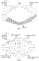
- FIGURE 4 illustrates a cross section 400 of a structure with actively driven electromagnetic shielding, according to certain embodiments.
- FIGURE 4 includes an actively shielded structure 420, electromagnets 425, external magnetic field 410, shielding magnetic field 428, and shielding magnetic field gap 430.
- FIGURE 4 illustrates an actively shielded structure 420 that is shielded from a plasma by shielding magnetic fields 428 produced by electromagnets 425.
- Shielding magnetic fields 428 produced by electromagnets 425, may divert external magnetic field 410, such as a magnetic field produced by internal magnetic coil structure 130 of FIGURE 1 , around actively shielded structure 420.
- a plasma may follow external magnetic field lines 410 and thus be diverted from contacting actively shielded structure 420 by shielding magnetic fields 428.
- electromagnets 425 require an external power source to produce shielding magnetic fields 428. Electromagnets 425 also may require cooling to prevent them from overheating, and may require cryogenic cooling if superconducting electromagnets are used as electromagnets 425. Additionally, because shielding magnetic fields 428 are not created in response to external magnetic field 410, but rather by power supplied to electromagnets 425, a system to control electromagnets 425 may be needed to ensure that shielding magnetic fields 428 are controlled to adequately compensate for variances in external magnetic field 410. Such a control system may have a lag time between when a change to external magnetic field 410 occurs and when adjustments are made to shielding magnetic fields 428.
- a actively shielded structure 420 when compared to a passively shield structure 320, is that the actively shielded structure 420 may be more complex than because it requires external power and a control system, and that an actively shielded structure 420 may not be able to compensate for changes in an external magnetic field as quickly as a passively shielded structure 320.
- An additional disadvantage of an actively shielded structure 420 is that magnetic field gaps 430 may be created between the shielding magnetic fields 428 produced by electromagnets 425. Magnetic field gaps 430 may create areas where external magnetic field 410 is not prevented from penetrating actively shielded structure 420. Accordingly, magnetic field gaps 430 may allow plasma following external magnetic field lines 410 to contact actively shielded structure 420. As explained elsewhere herein, contact between actively shielded structure 420 and a plasma may result in damage to actively shielded structure 420 by the plasma and of undesirable heat loss from the plasma to actively shielded structure 420.
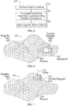
- FIGURE 5 illustrates a method 500 for shielding an object from a plasma using a superconducting material, according to certain embodiments.
- FIGURE 5 includes steps of cooling a superconducting material to a superconducting transition temperature at step 510, applying a magnetic field near or around an object including the superconducting material at step 520, and immersing the object in a plasma at step 530, which will be explained in detail below.
- a superconducting material that at least partially surrounds, or is disposed near the surface of the object may be cooled to a temperature at or below a superconducting transition temperature for the superconducting material.
- the superconducting material may demonstrate superconducting properties including having zero internal resistance to electrical current flow and excluding magnetic fields in which the superconducting material is placed.
- Cooling the superconducting material may be accomplished by a variety of means, such as those described with respect to cooling channels 230 of FIGURE 2 .
- the strength of a magnetic field that a superconducting material may be able exclude may depend on the temperature of the superconducting material.
- the superconducting material may be cooled to a temperature sufficient to cause the superconducting material to exclude the magnetic field.
- the superconducting material may be cooled to a temperature less than or equal 276 Kelvin.
- the superconducting material may be cooled to a temperature less than or equal to 200 Kelvin.
- the superconducting material may be cooled to a temperature less than or equal 138 Kelvin. In particular embodiments, the superconducting material may be cooled to a temperature less than or equal 30 Kelvin. In other embodiments, superconducting material 220 may be cooled to a temperature less than or equal 20 Kelvin. In yet other embodiments, superconducting material 220 may be cooled to a temperature less than or equal 10 Kelvin. In some embodiments, superconducting material 220 may be cooled to a temperature less than or equal 4 Kelvin.
- a magnetic field may be created in or applied to a space which contains the plasma formed at step 530.
- the magnetic field may be produced, such as a magnetic field produced by internal magnetic coil structure 130 of FIGURE 1 .
- the magnetic field may be present in the environment, such as a magnetic field permeating outer space. Because a superconducting material may exclude magnetic fields when cooled below the superconducting transition temperature of the material, the magnetic field may be excluded from the object after the superconducting material shielding the object has been cooled at step 510. As explained with respect to FIGURES 2 and 3 , since the plasma may follow the magnetic field, superconducting material may be protected from contact with the plasma by excluding the magnetic field.
- an object with superconducting material shielding such as shielded structure 210 of FIGURE 2
- a plasma may be created around a fixed object.
- a fusion plasma may be created inside of a fusion reactor, such as fusion plasma reactor chamber 110 of FIGURE 1 , in which an object, such as support structure 120 of FIGURE 1 is held fixed.
- plasmas that may be created include plasmas for plasma vapor deposition, plasma etching, plasma polymerization, or plasma exhaust streams from a plasma propulsion engine or ion propulsion engine.
- Other examples of a plasma in which an object may be immersed include plasmas in outer space, such as the solar wind.
- steps 510, 520, and 530 may occur in any order.
- a plasma may be produced inside of fusion plasma reactor chamber 110 at step 530, then a superconducting material shielding an object, such as support structure 120 of FIGURE 1 , may be cooled to temperature at or below its superconducting temperature at step 510, and finally the plasma and object may be exposed to a magnetic field generated by internal magnetic coil structure 130 at step 530.
- a magnetic field may be applied to a plasma prior to a superconducting material being cooled to a temperature at or below the superconducting transition temperature of the superconducting material.
- Shielding provided by a superconductor may also be beneficial in applications besides fusion reactors in which objects may be immersed in a flow of plasma.
- Charged particles that behave essentially as a low density plasma may be present throughout space outside of the Earth's magnetic field.
- the solar wind may be considered to be a low density plasma.
- Superconducting materials may product spacecraft from plasmas found in space. Additionally, numerous varieties of probes may be placed in plasmas for monitoring purposes. Superconducting materials may product such probes from damage when immersed in plasma, allowing the probe to operate for longer periods of time than an unshielded probe.
- FIGURE 6 illustrates a spacecraft 610 with superconducting material shielding immersed in a plasma 630, according to certain embodiments.
- Superconducting material surrounding all or a portion of spacecraft 610 may exclude magnetic fields, such as magnetic field 620, present in space and effectively shield spacecraft 610 from any plasma 630 or charged particles present in space.
- Such plasmas and charge particles could include solar radiation, cosmic rays, and any other form of charge particle found in space, and may follow the path of diverted magnetic field 625.
- Spacecraft 610 could operate in any environment of space including interplanetary space, interstellar space or intergalactic space.
- superconducting material may surround the entirety of spacecraft 610. In other embodiments superconducting material may surround a portion of spacecraft 610, such as a crew compartment in which a human crew lives or works, a compartment containing sensitive instruments, or a storage compartment. In other embodiments, superconducting material may be disposed within the envelope of spacecraft 610. For example, superconducting material may be disposed near the surface of spacecraft 610, such that it is able to exclude all or most of a magnetic field from contacting spacecraft 610, but is protected from incidental contact with plasma 630 by an outer skin of spacecraft 610.
- FIGURE 7 illustrates a probe 710 with superconducting material shielding immersed in a plasma 730, according to certain embodiments.
- Probe 710 may be any type of probe or sensor, including pressure sensors, temperature sensors, photo sensors, antenna, or any other device for receiving or measuring information.
- Probe 710 may be used to measure one or more properties of plasma 730 in which it is immersed, such as the temperature of plasma 730. However plasma 730 may damage probe 710 if probe 710 is not protected from contact with plasma 730.
- magnetic fields such as magnetic field 720
- Examples of environments in which a probe 710 with superconducting material shielding could be used include a fusion plasma contained in fusion plasma reactor chamber 110 of FIGURE 1 , a plasma for use in plasma vapor deposition, a plasma for use in plasma etching, a plasma for use in plasma polymerization, a plasma exhaust from a plasma propulsion engine or ion propulsion engine for a spacecraft, or any other magnetized plasma environment.
Landscapes
- Engineering & Computer Science (AREA)
- Physics & Mathematics (AREA)
- General Engineering & Computer Science (AREA)
- High Energy & Nuclear Physics (AREA)
- Plasma & Fusion (AREA)
- Microelectronics & Electronic Packaging (AREA)
- General Health & Medical Sciences (AREA)
- Health & Medical Sciences (AREA)
- Toxicology (AREA)
- Critical Care (AREA)
- Emergency Medicine (AREA)
- Remote Sensing (AREA)
- Aviation & Aerospace Engineering (AREA)
- Containers, Films, And Cooling For Superconductive Devices (AREA)
- Shielding Devices Or Components To Electric Or Magnetic Fields (AREA)
- Plasma Technology (AREA)
- Superconductors And Manufacturing Methods Therefor (AREA)
- Inorganic Compounds Of Heavy Metals (AREA)
Abstract
Description
- This invention relates generally to superconducting materials in plasmas.
- Superconductors are materials that conduct electrical current without any resistance. A unique property of superconductors is known as the Meissner effect, which is the property of superconductors to exclude magnetic fields from themselves. Most materials only display superconducting properties when cooled below a certain temperature, which may be referred to as the superconducting transition temperature or critical temperature. This temperature can vary between different superconducting materials, but is generally well below the freezing point of water.
- Plasmas are ionized gases. Because plasmas are ionized, and therefor electrically charged, plasmas can be manipulated using electric and magnetic fields. Plasmas are often hotter than room temperature, with some having temperatures of millions of degrees Kelvin. Because of their high temperature, it is often desirable to keep plasmas from coming into contact with objects immersed in a plasma or with the walls of a chamber used to contain a plasma.
- A fusion reactor includes a fusion plasma reactor chamber. A magnetic coil structure is disposed inside of the fusion plasma reactor chamber, and a structural component is also disposed inside of the fusion plasma reactor chamber. The structural component couples the magnetic coil structure to the fusion plasma reactor chamber. A superconducting material is disposed at least partially within the structural component. A plurality of cooling channels are disposed at least partially within the structural component. An insulating material is disposed at least partially within the structural component.
- A structural component in a plasma flow includes an interior structural component and a superconducting material disposed at least partially within the structural component and surrounding or adjacent to the interior structural component. A plurality of cooling channels are disposed at least partially within the structural component. An insulating material is disposed at least partially within the structural component.
- A method for protecting an object immersed in a plasma includes steps of applying a magnetic field through around a superconducting material, cooling a superconducting material that surrounds the object to a temperature sufficient to cause the superconducting material to exclude the magnetic field.
- Technical advantages of certain embodiments may include, protecting structural components from hot plasma without the need for an external power supply. Additionally, certain embodiments may prevent heat loss from a plasma by preventing it from contacting surfaces which could conduct heat away from the plasma. Some embodiments may also provide more complete protection of a structural component from a plasma when compared to actively powered, such as using electromagnets to generate magnetic fields, methods of protecting the structure. Further, some embodiments may offer reduced complexity when compared to actively powered methods of shielding the structure from a plasma.
- To provide a more complete understanding of the present invention and the features and advantages thereof, reference is made to the following description taken in conjunction with the accompanying drawings, in which:
-
FIGURE 1 illustrates a portion of a fusion reactor, according to certain embodiments; -
FIGURE 2 illustrates a structure shielded with a superconducting material, according to certain embodiments; -
FIGURE 3 illustrates a structure shielded with a superconducting material immersed in a plasma, according to certain embodiments; -
FIGURE 4 illustrates a structure with actively driven electromagnetic shielding immersed in a plasma, according to certain embodiments; -
FIGURE 5 illustrates a method for shielding an object from a plasma using a superconducting material, according to certain embodiments; -
FIGURE 6 illustrates a spacecraft with superconducting material shielding immersed in a plasma, according to certain embodiments; and -
FIGURE 7 illustrates a probe with superconducting material shielding immersed in a plasma, according to certain embodiments. - Embodiments of the present invention and its advantages are best understood by referring to
FIGURES 1 through 7 of the drawings, like numerals being used for like and corresponding parts of the various drawings. -
FIGURE 1 illustrates a portion of afusion reactor 100, according to certain embodiments.Fusion reactor portion 100 includes a fusionplasma reactor chamber 110, an internalmagnetic coil structure 130, andsupport structures 120.Support structures 120 may provide structural support for internalmagnetic coil structure 130, which may be suspended in fusionplasma reactor chamber 110. - Fusion
plasma reactor chamber 110 may contain a fusion plasma and provide an enclosed space for a fusion reaction to take place. Fusionplasma reactor chamber 110 may function as a structural mounting point forsupport structures 120, which may anchor internalmagnetic coil structure 130 to fusionplasma reactor chamber 110. Fusionplasma reactor chamber 110 may also hold any number of instruments or sensors needed to initiate, maintain, monitor, control, or stop a fusion plasma reaction. - Internal
magnetic coil structure 130 may generate a magnetic field that confines and directs a plasma contained within fusionplasma reactor chamber 110. Afusion reactor 100 may contain any number of internalmagnetic coil structures 130. In some embodiments, the magnetic field produced by internalmagnetic coil structure 130 may keep a hot plasma away from the walls of fusionplasma reactor chamber 110, which may prevent the plasma from damaging fusionplasma reactor chamber 110 or any instruments or sensors attached thereto. A magnetic field produced by internalmagnetic coil structure 130 may also compress a plasma contained in fusionplasma reactor chamber 110. Compressing a plasma may aid fusion by increasing the chance that hot plasma ions contact each other and undergo fusion. -
Support structures 120 may provide structural support for internalmagnetic coil structure 130 inside of fusionplasma reactor chamber 110. In some embodiments,support structures 120 may anchor internalmagnetic coil structure 130 to the walls of fusionplasma reactor chamber 110.Support structures 120 may also provide a path to supply power, cooling, and diagnostic leads to internalmagnetic coil structure 130. Magnetic fields produced by internalmagnetic coil structure 130 may not protectsupport structures 130 from contact with a plasma contained within fusionplasma reactor chamber 110. In some embodiments, without a means of protection, magnetic fields produced by internalmagnetic coil structure 130 may penetratesupport structures 120, resulting in contact between a plasma following the magnetic field produced by internalmagnetic coil structure 130 andsupport structures 120. Contact between a plasma andsupport structures 120 may damage the support structures and ultimately lead to their failure due to the high temperature and energy of the plasma. Likewise, contact between a hot plasma andsupport structures 120 may transfer heat out of the plasma and intosupport structures 120, thereby decreasing the temperature of the plasma and reducing the efficiency of any fusion reaction taking place in the plasma. Accordingly, it is desirable to prevent contact between a plasma contained in fusionplasma reactor chamber 110 andsupport structures 120 to prevent damage to the support structures and to maintain the temperature of the plasma. -
FIGURE 2 shows across section 200 of a passively shieldedsupport structure 120 viewed from an angle viewed along the radial direction as defined relative to the axis of symmetry inFIG. 1 , in other words, a cross-section viewed "top-down" into shieldedsupport structure 120.Support structure 120 includes a shieldedstructure 210,superconducting material 220,cooling channels 230,cooling fluid 240, andinsulating material 250. -
Shielded structure 210 may include structural supports, such as beams or pipes used to anchor internalmagnetic coil structure 130 to the walls of fusionplasma reactor chamber 110.Shielded structure 210 may also include routing for power and instrumentation cables for internalmagnetic coil structure 130. In some embodiments, shieldedstructure 210 may include pipes, channels or tubes for cooling internalmagnetic coil structure 130 illustrated inFIGURE 1 . In some embodiments, shieldedstructure 210 may have portions that extend beyondsuperconducting material 220, such thatsuperconducting material 220 is disposed within the envelope ofsupport structure 120. For example, a thin section of shieldedstructure 210 form the exterior ofsupport structure 120, such thatsuperconducting material 220 is disposed interior to the thin portion of shieldedstructure 210. In another embodiment, a protective layer of material may be disposed ontosuperconducting material 220 to protect superconducting material from incidental contact with a plasma. -
Superconducting material 220 may be any superconducting material that is disposed to provide sufficient coverage of shieldedstructure 210. In some embodiments, super conductingmaterial 220 may be a thin superconducting tape applied to shieldedstructure 210. Atape superconducting material 220 may be wrapped aroundstructure 210, or applied in strips or patches to shieldedstructure 210 so as to cover shieldedstructure 210. In some embodiments, layers of a superconducting tape may overlap other layers of a super conducting tape. In particular embodiments, multiple layers of superconducting tape may be used to ensure adequate surface area ofsuperconducting material 220, in a similar to multiple windings of a wire in an electromagnet. - In other embodiments,
superconducting material 220 may be tiles that are layered onto shieldedstructure 210. Such superconducting tiles may be arranged in contact with one another in such a way that shieldedstructure 210 is not exposed to a plasma. Such tiles may be arranged side by side or be layered, in a manner similar to scales or shingles, in such a manner that shieldedstructure 210 is not exposed to a plasma. In other embodiments,superconducting material 220 may be applied to structure 210 as a coating, such as a paint or powder coating. In yet other embodiments,superconducting material 220 may be a pre-fabricated shell that is placed around shieldedstructure 210 before or after installation of shieldedstructure 210 into fusionplasma reactor chamber 110. In such embodiments,superconducting material 220 may be fabricated as a single shell surrounding shieldedstructure 210 or as a shell including multiple pieces that are assembled to surround shieldedstructure 210. - In some embodiments, any of the arrangements of
superconducting material 220 described above may be disposed within the envelope of shieldedstructure 210. For example,superconducting material 220 may be disposed near the surface of shieldedstructure 210, such thatsuperconducting material 220 is able to sufficiently exclude magnetic fields around shieldedstructure 210 without being exposed to direct contact with any plasma. -
Superconducting material 220 may be any superconducting material. Depending on the material chosen, a cooling fluid with an appropriate temperature forsuperconducting material 220 should be selected. In some embodiments,superconducting material 220 may be a member of the class of superconductors known as "high temperature" superconductors. In general, high temperature superconductors are materials that become superconducting at a temperature above 30 Kelvin. Examples of classes of high temperature superconductors include, but are not limited to: cuprate superconductors, which include lanthanum barium copper oxide superconductors, thallium barium calcium copper oxide superconductors, strontium calcium copper oxide superconductors, and yttrium barium copper oxide superconductors; and iron pnictide superconductors. - In some embodiments,
superconducting material 220 may be cooled to a temperature sufficient to causesuperconducting material 220 to exclude a magnetic field, such as a magnetic field produced by internalmagnetic coil structure 130 ofFIGURE 1 . In someembodiments superconducting material 220 may be cooled to a temperature less than or equal 276 Kelvin. In some embodiments,superconducting material 220 may be cooled to a temperature less than or equal to 200 Kelvin. In particular embodiments,superconducting material 220 may be cooled to a temperature less than or equal 138 Kelvin. In particular embodiments,superconducting material 220 may be cooled to a temperature less than or equal 30 Kelvin. In other embodiments,superconducting material 220 may be cooled to a temperature less than or equal 20 Kelvin. In yet other embodiments,superconducting material 220 may be cooled to a temperature less than or equal 10 Kelvin. In some embodiments,superconducting material 220 may be cooled to a temperature less than or equal 4 Kelvin. -
Superconducting material 220 may exclude external magnetic fields, such as a magnetic field produced by internalmagnetic coil structure 130, because an external magnetic field causes a current to form withinsuperconducting material 220 that produces a magnetic field that cancels out the external magnetic field. These internal currents may be created near the surface ofsuperconducting material 220. Therefore, thin layers ofsuperconducting material 220, such as the superconducting tape described above, may be sufficient to exclude magnetic fields.Superconducting material 220 may have a limit to the strength of the internal current thatsuperconducting material 220 can support, and therefore a limit to the strength of the magnetic field thatsuperconducting material 220 can exclude. - In some embodiments, the internal current that
superconducting material 220 can support, and therefore the strength of an external magnetic field thatsuperconducting material 220 can exclude, may depend on the temperature ofsuperconducting material 220.Superconducting material 220 may be able to support a larger internal current and exclude a stronger magnetic field the farther it is cooled below its superconducting transition temperature. For example,superconducting material 220 may be able to support five times as much current when cooled to 30 K as it can when cooled to 77 K. Therefore, in some embodiments, it may be important to maintain cooling ofsuperconducting material 220 to ensure a temperature is maintained that is sufficient forsuperconducting material 220 to be able to exclude a magnetic field produced inside of fusionplasma reactor chamber 110. - Cooling
channels 230 may include pipes, tubes, passages or any other means of transporting a cooling fluid 240 in proximity tosuperconducting material 220. In some embodiments, coolingchannels 230 may also provide cooling to internalmagnetic coil structure 130. In some embodiments, coolingchannels 230 may provide for cooling fluid 240 to be in direct contact withsuperconducting material 220. In other embodiments, coolingchannels 230 may be constructed of a material with a high heat transfer coefficient, such as most metals. In these embodiments,superconducting material 220 may be in contact with the high heat transfer material of coolingchannel 230, with the high heat transfer material transferring heat fromsuperconducting material 220 to coolingfluid 240 within coolingchannel 220. Examples of acceptable high heat transfer materials include, but are not limited to, copper, aluminum, iron, titanium, silver, gold, any other metal used in cryogenic applications, and alloys thereof. In someembodiments cooling channels 220 may include insulating breaks to improve thermal isolation of coolingchannels 220. - Cooling
fluid 240 may be any acceptable liquid, gas, or other fluid with a temperature low enough to coolsuperconducting material 220 to or below its superconducting transition temperature. Some examples of cooling fluids or gases include liquid oxygen, liquid nitrogen, liquid helium, liquid argon, liquid neon, and gases of thereof, or any other fluid or gas with a temperature at or below the superconducting transition temperature ofsuperconducting material 220. - In some embodiments, cooling
channels 230 may be insulated on the side of coolingchannels 230 that is closest to shieldedstructure 210 by insulatingmaterial 250. Insulation betweencooling channels 230 and shieldedstructure 210 may prevent transfer of heat from shieldedstructure 210 into coolingchannels 230, and therefore may increase cooling capacity of coolingchannels 230 by preventing loss of cooling capacity through coolingchannels 230 cooling shieldedstructure 210. Insulatingmaterial 250 may be disposed in any appropriate manner throughout shieldedstructure 210 to ensure adequate insulating of coolingchannels 230 andsuperconducting material 220. Insulation betweencooling channels 230 may be any form of insulation used in cryogenic applications. For example, insulation may include polymer foams, aerogels, fiberglass, mineral wool or other insulating materials. In some embodiments, insulation betweencooling channels 230 and shieldedstructure 210 may be a double walled vacuum structure, similar to those found in Dewar flasks or bottles commonly used for storing cryogenic liquids. Such a structure may have two walls separated by a space which contains a vacuum, which provides insulation between the environments separate by the two walls. In some embodiments, insulatingmaterial 250 may also be disposed betweensuperconducting material 220 and the surface of shieldedstructure 210. In such an embodiment, insulatingmaterial 250 may prevent or slow heat from shieldedstructure 210 from being conducted intosuperconducting material 250 and thereby preserve the strength of magnetic fields thatsuperconducting material 220 is able to exclude. - In other embodiments, cooling
channels 230 may not carry a fluid but may be thermoelectric cooling units. In some embodiments, a thermoelectric cooler may be disposed betweensuperconducting material 220 and coolingchannels 230. -
FIGURE 3 illustrates across section 300 of shieldedstructure 320 shielded with a superconducting material immersed in a plasma, according to certain embodiments. Shieldedstructure 320 may be a support structure, such assupport structure 120 ofFIGURE 1 , that is shielded by a superconducting material, such assuperconducting material 220 ofFIGURE 2 . In other embodiments, shielded structure may be any other structure or object immersed in a plasma, such as aspacecraft 610 ofFIGURE 6 , or probe 710 ofFIGURE 7 . When exposed to a magnetic field, such as a magnetic field generated by internalmagnetic coil structure 130, the superconducting material shielding shieldedstructure 320 may exclude the magnetic field. InFIGURE 3 ,magnetic field lines 310 are pushed or bent around shieldedstructure 320 because the superconducting material excludes the magnetic field. Because a plasma is electrically charged, it may follow magnetic field lines 310. Therefore by excludingmagnetic field lines 310,superconducting material 220 may prevent plasma 330 from contactingstructure 320. Plasma 330 may be any plasma. In a particular embodiment, plasma 330 may be a fusion plasma contained within fusionplasma reactor chamber 110 ofFIGURE 1 . This method of shieldingstructure 320 from a plasma using a superconducting material may be referred to as "passive" shielding, because no external power needs to be supplied to the superconducting material for it to exclude the magnetic field, as long as the super conducting material is adequately cooled. - In some
embodiments superconducting material 220 may sufficiently excludemagnetic field lines 310 to prevent any plasma from contacting shieldedstructure 320. In otherembodiments superconducting material 220 may sufficiently excludemagnetic field lines 310 to prevent the majority of a plasma from contacting shieldedstructure 320. In some embodiments,superconducting material 220 may sufficiently excludemagnetic field lines 310 to prevent more than 99.9% of plasma 330 from contactingstructure 320. In some embodiments,superconducting material 220 may sufficiently excludemagnetic field lines 310 to prevent more than 99% of plasma 330 from contacting shieldedstructure 320. In some embodiments,superconducting material 220 may sufficiently excludemagnetic field lines 310 to prevent more than 90% of plasma 330 from contacting shieldedstructure 320. - Preventing contact between a plasma and shielded
structure 320 using a superconducting material may have at least two advantages. First, damage to shieldedstructure 320 by the hot plasma may be prevented. This could prevent failure of a fusion reactor and increase time intervals between maintenance on the reactor. Second, preventing contact between a plasma and shieldedstructure 320 may prevent heat loss from the plasma to shieldedstructure 320, which may increase the efficiency of a fusion reaction. An additional benefit of using a superconducting material to passively shieldstructure 320, is that the ability of the superconducting material to exclude an external magnetic fields may automatically and rapidly adjust in response to variances in the external magnetic field. This may eliminate the need for complex control systems, as described below with reference toFIGURE 4 . - Another advantage of a structure passively shielded by a superconducting material is illustrated by
FIGURE 4 , which illustrates across section 400 of a structure with actively driven electromagnetic shielding, according to certain embodiments.FIGURE 4 includes an actively shieldedstructure 420,electromagnets 425, externalmagnetic field 410, shieldingmagnetic field 428, and shieldingmagnetic field gap 430. UnlikeFIGURES 1 through 3 , which illustrate a structure passively shielded by a superconducting material that excludes magnetic fields,FIGURE 4 illustrates an actively shieldedstructure 420 that is shielded from a plasma by shieldingmagnetic fields 428 produced byelectromagnets 425. - Shielding
magnetic fields 428, produced byelectromagnets 425, may divert externalmagnetic field 410, such as a magnetic field produced by internalmagnetic coil structure 130 ofFIGURE 1 , around actively shieldedstructure 420. A plasma may follow externalmagnetic field lines 410 and thus be diverted from contacting actively shieldedstructure 420 by shieldingmagnetic fields 428. - However, unlike
superconducting material 220 ofFIGURE 2 ,electromagnets 425 require an external power source to produce shieldingmagnetic fields 428.Electromagnets 425 also may require cooling to prevent them from overheating, and may require cryogenic cooling if superconducting electromagnets are used aselectromagnets 425. Additionally, because shieldingmagnetic fields 428 are not created in response to externalmagnetic field 410, but rather by power supplied toelectromagnets 425, a system to controlelectromagnets 425 may be needed to ensure that shieldingmagnetic fields 428 are controlled to adequately compensate for variances in externalmagnetic field 410. Such a control system may have a lag time between when a change to externalmagnetic field 410 occurs and when adjustments are made to shieldingmagnetic fields 428. Therefore, disadvantages of a actively shieldedstructure 420 when compared to a passively shieldstructure 320, is that the actively shieldedstructure 420 may be more complex than because it requires external power and a control system, and that an actively shieldedstructure 420 may not be able to compensate for changes in an external magnetic field as quickly as a passively shieldedstructure 320. - An additional disadvantage of an actively shielded
structure 420 is thatmagnetic field gaps 430 may be created between the shieldingmagnetic fields 428 produced byelectromagnets 425.Magnetic field gaps 430 may create areas where externalmagnetic field 410 is not prevented from penetrating actively shieldedstructure 420. Accordingly,magnetic field gaps 430 may allow plasma following externalmagnetic field lines 410 to contact actively shieldedstructure 420. As explained elsewhere herein, contact between actively shieldedstructure 420 and a plasma may result in damage to actively shieldedstructure 420 by the plasma and of undesirable heat loss from the plasma to actively shieldedstructure 420. -
FIGURE 5 illustrates amethod 500 for shielding an object from a plasma using a superconducting material, according to certain embodiments.FIGURE 5 includes steps of cooling a superconducting material to a superconducting transition temperature atstep 510, applying a magnetic field near or around an object including the superconducting material atstep 520, and immersing the object in a plasma atstep 530, which will be explained in detail below. - At
step 510, a superconducting material that at least partially surrounds, or is disposed near the surface of the object, such assuperconducting material 220 ofFIGURE 2 , may be cooled to a temperature at or below a superconducting transition temperature for the superconducting material. At or below the superconducting transition temperature, the superconducting material may demonstrate superconducting properties including having zero internal resistance to electrical current flow and excluding magnetic fields in which the superconducting material is placed. - Cooling the superconducting material may be accomplished by a variety of means, such as those described with respect to cooling
channels 230 ofFIGURE 2 . As described with respect toFIGURE 2 , the strength of a magnetic field that a superconducting material may be able exclude may depend on the temperature of the superconducting material. In some embodiments, the superconducting material may be cooled to a temperature sufficient to cause the superconducting material to exclude the magnetic field. In some embodiments the superconducting material may be cooled to a temperature less than or equal 276 Kelvin. In some embodiments, the superconducting material may be cooled to a temperature less than or equal to 200 Kelvin. In particular embodiments, the superconducting material may be cooled to a temperature less than or equal 138 Kelvin. In particular embodiments, the superconducting material may be cooled to a temperature less than or equal 30 Kelvin. In other embodiments,superconducting material 220 may be cooled to a temperature less than or equal 20 Kelvin. In yet other embodiments,superconducting material 220 may be cooled to a temperature less than or equal 10 Kelvin. In some embodiments,superconducting material 220 may be cooled to a temperature less than or equal 4 Kelvin. - At
step 520, a magnetic field may be created in or applied to a space which contains the plasma formed atstep 530. In some embodiments the magnetic field may be produced, such as a magnetic field produced by internalmagnetic coil structure 130 ofFIGURE 1 . In other embodiments, the magnetic field may be present in the environment, such as a magnetic field permeating outer space. Because a superconducting material may exclude magnetic fields when cooled below the superconducting transition temperature of the material, the magnetic field may be excluded from the object after the superconducting material shielding the object has been cooled atstep 510. As explained with respect toFIGURES 2 and3 , since the plasma may follow the magnetic field, superconducting material may be protected from contact with the plasma by excluding the magnetic field. - At
step 530 an object with superconducting material shielding, such as shieldedstructure 210 ofFIGURE 2 , may be immersed in a plasma. In some embodiments, atstep 510, a plasma may be created around a fixed object. For example, a fusion plasma may be created inside of a fusion reactor, such as fusionplasma reactor chamber 110 ofFIGURE 1 , in which an object, such assupport structure 120 ofFIGURE 1 is held fixed. Other examples of plasmas that may be created include plasmas for plasma vapor deposition, plasma etching, plasma polymerization, or plasma exhaust streams from a plasma propulsion engine or ion propulsion engine. Other examples of a plasma in which an object may be immersed include plasmas in outer space, such as the solar wind. - Although illustrated sequentially in
FIGURE 5 ,steps plasma reactor chamber 110 atstep 530, then a superconducting material shielding an object, such assupport structure 120 ofFIGURE 1 , may be cooled to temperature at or below its superconducting temperature atstep 510, and finally the plasma and object may be exposed to a magnetic field generated by internalmagnetic coil structure 130 atstep 530. Alternatively, a magnetic field may be applied to a plasma prior to a superconducting material being cooled to a temperature at or below the superconducting transition temperature of the superconducting material. - Shielding provided by a superconductor may also be beneficial in applications besides fusion reactors in which objects may be immersed in a flow of plasma. Charged particles that behave essentially as a low density plasma may be present throughout space outside of the Earth's magnetic field. For example, the solar wind may be considered to be a low density plasma. Superconducting materials may product spacecraft from plasmas found in space. Additionally, numerous varieties of probes may be placed in plasmas for monitoring purposes. Superconducting materials may product such probes from damage when immersed in plasma, allowing the probe to operate for longer periods of time than an unshielded probe.
-
FIGURE 6 illustrates aspacecraft 610 with superconducting material shielding immersed in aplasma 630, according to certain embodiments. Superconducting material surrounding all or a portion ofspacecraft 610 may exclude magnetic fields, such asmagnetic field 620, present in space and effectively shieldspacecraft 610 from anyplasma 630 or charged particles present in space. Such plasmas and charge particles could include solar radiation, cosmic rays, and any other form of charge particle found in space, and may follow the path of divertedmagnetic field 625.Spacecraft 610 could operate in any environment of space including interplanetary space, interstellar space or intergalactic space. - In some embodiments, superconducting material may surround the entirety of
spacecraft 610. In other embodiments superconducting material may surround a portion ofspacecraft 610, such as a crew compartment in which a human crew lives or works, a compartment containing sensitive instruments, or a storage compartment. In other embodiments, superconducting material may be disposed within the envelope ofspacecraft 610. For example, superconducting material may be disposed near the surface ofspacecraft 610, such that it is able to exclude all or most of a magnetic field from contactingspacecraft 610, but is protected from incidental contact withplasma 630 by an outer skin ofspacecraft 610. -
FIGURE 7 illustrates aprobe 710 with superconducting material shielding immersed in aplasma 730, according to certain embodiments.Probe 710 may be any type of probe or sensor, including pressure sensors, temperature sensors, photo sensors, antenna, or any other device for receiving or measuring information.Probe 710 may be used to measure one or more properties ofplasma 730 in which it is immersed, such as the temperature ofplasma 730. Howeverplasma 730 may damage probe 710 ifprobe 710 is not protected from contact withplasma 730. Surroundingprobe 710 with a superconducting material, in a manner similar tosuperconducting material 220 described with respect toFIGURE 2 , may exclude magnetic fields, such asmagnetic field 720, aroundprobe 710 and thereby protectprobe 710 fromplasma 730 by divertingplasma 730 along the excludedmagnetic field 725 in a manner similar to that described with respect toFIGURE 3 . - Examples of environments in which a
probe 710 with superconducting material shielding could be used include a fusion plasma contained in fusionplasma reactor chamber 110 ofFIGURE 1 , a plasma for use in plasma vapor deposition, a plasma for use in plasma etching, a plasma for use in plasma polymerization, a plasma exhaust from a plasma propulsion engine or ion propulsion engine for a spacecraft, or any other magnetized plasma environment. - Modifications, additions, or omissions may be made to the methods described herein without departing from the scope of the invention. For example, the steps may be combined, modified, or deleted where appropriate, and additional steps may be added. Additionally, the steps may be performed in any suitable order without departing from the scope of the present disclosure.
- Although the present invention has been described with several embodiments, a myriad of changes, variations, alterations, transformations, and modifications may be suggested to one skilled in the art, and it is intended that the present invention encompass such changes, variations, alterations, transformations, and modifications as fall within the scope of the appended claims.
Claims (13)
- A fusion reactor comprising:a fusion plasma reactor chamber;a magnetic coil structure disposed inside of the fusion plasma reactor chamber;a structural component disposed inside of the fusion plasma reactor chamber, wherein the structural component couples the magnetic coil structure to the fusion plasma reactor chamber;a superconducting material disposed at least partially within the structural component;a plurality of cooling channels disposed at least partially within the structural component; andan insulating material disposed at least partially within the structural component.
- A structural component configured to be at least partially within a plasma flow, comprising:an interior structural component;a superconducting material at least partially surrounding the interior structural component;a plurality of cooling channels disposed at least partially within the structural component; andan insulating material disposed at least partially within the structural component.
- The fusion reactor of claim 1 or the structural component of claim 2, wherein the plurality of cooling channels comprises a plurality of metal tubes.
- The fusion reactor of claim 1 or of claim 3, or the structural component of claim 2 or of claim 3, wherein the superconducting material comprises a superconducting tape.
- The fusion reactor of claim 1 or of claim 3 or of claim 4, or the structural component of claim 2 or of claim 3 or of claim 4, wherein the superconducting material comprises a plurality of superconducting tiles.
- The fusion reactor of claim 1 or of any of claims 3 to 5, or the structural component of claim 2 or of any of claims 3 to 5, wherein the superconducting material is cooled to a temperature equal to or below a superconducting transition temperature of the superconducting material.
- The fusion reactor of claim 1 or of any of claims 3 to 6, wherein the superconducting material excludes a magnetic field from penetrating the structural component; or
the structural component of claim 2 or of any of claims 3 to 6, wherein the superconducting material excludes a magnetic field from penetrating the interior structural component. - The fusion reactor of claim 1 or of any of claims 3 to 7, or the structural component of claim 2 or of any of claims 3 to 7, wherein the insulator comprises two walls separated by a near vacuum.
- The fusion reactor of claim 1 or of any of claims 3 to 8, or the structural component of claim 2 or of any of claims 3 to 8, wherein a cooling fluid is circulated through the plurality of cooling channels.
- The fusion reactor of claim 1 or of any of claims 3 to 9, further comprising a fusion plasma contained inside of the fusion plasma reactor chamber.
- A method for protecting an object configured to be at least partially immersed in a plasma, comprising:applying a magnetic field around a superconducting material; andcooling the superconducting material to a temperature sufficient to cause the superconducting material to exclude the magnetic field, wherein the superconducting material is disposed at least partially within the object.
- The method of claim 11, wherein a cooling fluid is used to cool the superconducting material.
- The method of claim 11 or of claim 12, wherein the temperature sufficient to cause the superconducting material to exclude the magnetic field is less than or equal to 200 Kelvin.
Applications Claiming Priority (1)
| Application Number | Priority Date | Filing Date | Title |
|---|---|---|---|
| US15/873,614 US10784001B2 (en) | 2018-01-17 | 2018-01-17 | Passive magnetic shielding of structures immersed in plasma using superconductors |
Publications (2)
| Publication Number | Publication Date |
|---|---|
| EP3514801A1 true EP3514801A1 (en) | 2019-07-24 |
| EP3514801B1 EP3514801B1 (en) | 2020-09-09 |
Family
ID=65003308
Family Applications (1)
| Application Number | Title | Priority Date | Filing Date |
|---|---|---|---|
| EP19150580.9A Active EP3514801B1 (en) | 2018-01-17 | 2019-01-07 | Passive magnetic shielding of structures immersed in plasma using superconductors |
Country Status (6)
| Country | Link |
|---|---|
| US (3) | US10784001B2 (en) |
| EP (1) | EP3514801B1 (en) |
| JP (1) | JP7166941B2 (en) |
| KR (1) | KR102446787B1 (en) |
| AU (1) | AU2019200039B2 (en) |
| CA (1) | CA3029223C (en) |
Cited By (1)
| Publication number | Priority date | Publication date | Assignee | Title |
|---|---|---|---|---|
| GB2595052A (en) * | 2021-04-20 | 2021-11-17 | Lynley Ashley Adrian | Fusion reactor magnetic plasma shield |
Families Citing this family (1)
| Publication number | Priority date | Publication date | Assignee | Title |
|---|---|---|---|---|
| EP3819913A1 (en) * | 2019-11-11 | 2021-05-12 | JFP Jäderberg Fusion Power AB | Plasma confinement device and method for plasma confinement |
Citations (3)
| Publication number | Priority date | Publication date | Assignee | Title |
|---|---|---|---|---|
| US3639672A (en) * | 1969-02-21 | 1972-02-01 | Inst Plasmaphysik Gmbh | Electrical conductor |
| US8809824B1 (en) * | 2010-12-13 | 2014-08-19 | The Boeing Company | Cryogenically cooled radiation shield device and associated method |
| EP2981972A2 (en) * | 2013-04-03 | 2016-02-10 | Lockheed Martin Corporation | System for supporting structures immersed in plasma |
Family Cites Families (39)
| Publication number | Priority date | Publication date | Assignee | Title |
|---|---|---|---|---|
| US2138362A (en) * | 1935-10-24 | 1938-11-29 | Anaconda Wire & Cable Co | Electric cable and method of making same |
| US3117912A (en) | 1954-06-17 | 1964-01-14 | Donald H Imhoff | Method of producing neutrons |
| US3012955A (en) | 1958-08-20 | 1961-12-12 | Russell M Kulsrud | High temperature reactor |
| US4023043A (en) | 1974-08-16 | 1977-05-10 | Megatherm Corporation | Computerized peak-shaving system for alleviating electric utility peak loads |
| US4274919A (en) | 1977-11-14 | 1981-06-23 | General Atomic Company | Systems for merging of toroidal plasmas |
| US4252608A (en) | 1979-03-16 | 1981-02-24 | The United States Of America As Represented By The United States Department Of Energy | Generating end plug potentials in tandem mirror plasma confinement by heating thermal particles so as to escape low density end stoppering plasmas |
| JPS5791486A (en) | 1980-11-28 | 1982-06-07 | Hitachi Ltd | Toroidal nuclear fusion equipment |
| JP2519200B2 (en) | 1984-03-07 | 1996-07-31 | 株式会社日立製作所 | Superconducting device |
| DE3416843A1 (en) | 1984-05-07 | 1985-11-14 | Max-Planck-Gesellschaft zur Förderung der Wissenschaften e.V., 3400 Göttingen | ACTIVE COOLED HEAT SHIELD |
| JPS6444888A (en) * | 1987-08-14 | 1989-02-17 | Hitachi Ltd | Nuclear fusion device |
| JPH0194602A (en) | 1987-10-06 | 1989-04-13 | Mitsubishi Electric Corp | Helical superconducting coil device |
| JPH01119791A (en) | 1987-11-04 | 1989-05-11 | Toshiba Corp | Fusion device |
| JPH01216097A (en) * | 1988-02-22 | 1989-08-30 | Toshiba Corp | Magnetic shield type turbo molecular pump |
| DE3828902A1 (en) | 1988-08-25 | 1990-03-08 | Max Planck Gesellschaft | HEAT SHIELD |
| JPH0339690A (en) | 1989-07-06 | 1991-02-20 | Osamu Motojima | Plasma fusion experimental device |
| JPH0339680A (en) | 1989-07-07 | 1991-02-20 | Hitachi Medical Corp | Scintillation camera |
| US4921661A (en) | 1989-11-03 | 1990-05-01 | The United States Of America As Represented By The United States Department Of Energy | Segmented saddle-shaped passive stabilization conductors for toroidal plasmas |
| DE69026923T2 (en) * | 1990-01-22 | 1996-11-14 | Werner K Steudtner | Nuclear fusion reactor |
| JPH05101923A (en) * | 1991-10-07 | 1993-04-23 | Fujikura Ltd | Method for manufacturing oxide superconducting coil |
| JP3349539B2 (en) * | 1993-03-01 | 2002-11-25 | 株式会社日立製作所 | Insulated support device |
| JPH0722231A (en) | 1993-06-21 | 1995-01-24 | Toshiba Corp | Superconducting magnet for MRI equipment |
| US5488339A (en) | 1993-11-23 | 1996-01-30 | General Electric Company | Passive shielding of mobile magnetic resonance imaging magnet |
| US5448214A (en) | 1994-06-15 | 1995-09-05 | General Electric Company | Open MRI magnet with superconductive shielding |
| JPH0954179A (en) | 1995-08-10 | 1997-02-25 | Japan Atom Energy Res Inst | Neutral particle injector |
| JP3692625B2 (en) * | 1996-06-20 | 2005-09-07 | 富士電機システムズ株式会社 | Superconducting power transmission cable |
| JP3706900B2 (en) * | 1999-07-07 | 2005-10-19 | 国立大学法人東北大学 | How to use bitter type low temperature resistance magnet |
| JP2001066389A (en) | 1999-08-27 | 2001-03-16 | Japan Atom Energy Res Inst | First wall / breeding blanket |
| US6593539B1 (en) | 2000-02-25 | 2003-07-15 | George Miley | Apparatus and methods for controlling charged particles |
| US6611106B2 (en) | 2001-03-19 | 2003-08-26 | The Regents Of The University Of California | Controlled fusion in a field reversed configuration and direct energy conversion |
| JP4676095B2 (en) | 2001-07-12 | 2011-04-27 | 古河電気工業株式会社 | Superconducting cable |
| JP2003155542A (en) | 2001-11-21 | 2003-05-30 | Japan Atom Energy Res Inst | High Mn non-magnetic steel for superconducting magnet structural materials with excellent hot workability and resistance to heat embrittlement after heat treatment for forming superconductors |
| JP2006108560A (en) * | 2004-10-08 | 2006-04-20 | Kyushu Electric Power Co Inc | Current leads for superconducting equipment |
| AT8158U1 (en) | 2004-10-27 | 2006-02-15 | Plansee Ag | MONOBLOCK COOLING COMPONENT |
| US9036765B2 (en) | 2006-05-30 | 2015-05-19 | Advanced Fusion Systems Llc | Method and system for inertial confinement fusion reactions |
| US8588876B1 (en) * | 2011-03-10 | 2013-11-19 | The Florida State University Research Foundation, Inc. | Electric joint design to be used in electromagnetic coils made with high-temperature superconducting tape, aspected wire, or cable |
| US9928927B2 (en) * | 2013-04-03 | 2018-03-27 | Lockheed Martin Corporation | Heating plasma for fusion power using magnetic field oscillation |
| GB2510447B (en) * | 2013-09-13 | 2015-02-18 | Tokamak Energy Ltd | Toroidal field coil for use in a fusion reactor |
| GB2528272B (en) | 2014-07-15 | 2017-06-21 | Tokamak Energy Ltd | Shielding materials for fusion reactors |
| GB201515726D0 (en) * | 2015-09-04 | 2015-10-21 | Tokamak Energy Ltd | Support structures for HTS magnets |
-
2018
- 2018-01-17 US US15/873,614 patent/US10784001B2/en active Active
-
2019
- 2019-01-04 AU AU2019200039A patent/AU2019200039B2/en active Active
- 2019-01-07 EP EP19150580.9A patent/EP3514801B1/en active Active
- 2019-01-08 CA CA3029223A patent/CA3029223C/en active Active
- 2019-01-14 KR KR1020190004638A patent/KR102446787B1/en active Active
- 2019-01-17 JP JP2019005653A patent/JP7166941B2/en active Active
-
2020
- 2020-09-21 US US17/026,464 patent/US11776700B2/en active Active
-
2023
- 2023-08-29 US US18/457,622 patent/US20230402196A1/en active Pending
Patent Citations (3)
| Publication number | Priority date | Publication date | Assignee | Title |
|---|---|---|---|---|
| US3639672A (en) * | 1969-02-21 | 1972-02-01 | Inst Plasmaphysik Gmbh | Electrical conductor |
| US8809824B1 (en) * | 2010-12-13 | 2014-08-19 | The Boeing Company | Cryogenically cooled radiation shield device and associated method |
| EP2981972A2 (en) * | 2013-04-03 | 2016-02-10 | Lockheed Martin Corporation | System for supporting structures immersed in plasma |
Cited By (1)
| Publication number | Priority date | Publication date | Assignee | Title |
|---|---|---|---|---|
| GB2595052A (en) * | 2021-04-20 | 2021-11-17 | Lynley Ashley Adrian | Fusion reactor magnetic plasma shield |
Also Published As
| Publication number | Publication date |
|---|---|
| US20230402196A1 (en) | 2023-12-14 |
| BR102019000825A2 (en) | 2019-07-30 |
| JP2019124690A (en) | 2019-07-25 |
| AU2019200039A1 (en) | 2019-08-01 |
| US10784001B2 (en) | 2020-09-22 |
| KR102446787B1 (en) | 2022-09-22 |
| EP3514801B1 (en) | 2020-09-09 |
| US20190221322A1 (en) | 2019-07-18 |
| KR20190088018A (en) | 2019-07-25 |
| AU2019200039B2 (en) | 2021-12-02 |
| CA3029223A1 (en) | 2019-07-17 |
| BR102019000825A8 (en) | 2023-04-04 |
| CA3029223C (en) | 2023-08-15 |
| JP7166941B2 (en) | 2022-11-08 |
| US20210005333A1 (en) | 2021-01-07 |
| US11776700B2 (en) | 2023-10-03 |
Similar Documents
| Publication | Publication Date | Title |
|---|---|---|
| US20230402196A1 (en) | Passive magnetic shielding of structures immersed in plasma using superconductors | |
| CN102349119B (en) | Method and apparatus for electrical, mechanical and thermal isolation of superconductive magnets | |
| DK2698794T3 (en) | Arrangement with at least one superconducting cable | |
| US9090360B2 (en) | Cryogenically cooled radiation shield device and associated method | |
| US12156323B2 (en) | High-temperature superconducting plasma thruster system having variable temperature ranges and being applied in space | |
| US6730851B2 (en) | Superconducting cable and current transmission and/or distribution network including the superconducting cable | |
| US9685260B2 (en) | Method of cooling a superconductive cable | |
| US10825594B2 (en) | System for generating a vector magnetic field | |
| Stamm et al. | Superconducting power cable design with hybrid cryogenic media-gaseous helium for cooling and liquid nitrogen for dielectric insulation | |
| BR102019000825B1 (en) | FUSION REACTOR FOR SHIELDING PLASMA-IMMERSED STRUCTURES USING SUPERCONDUCTING MATERIAL | |
| Bögel et al. | Magnetohydrodynamic enhanced entry system for space transportation (MEESST) as a key building block for future exploration missions | |
| EP1195777B1 (en) | Superconducting cable | |
| JP7477959B2 (en) | Superconducting coil device and current lead structure for superconducting coil | |
| La Rosa Betancourt et al. | A superconductor-based magnetohydrodynamic shielding system for hypersonic re-entry: meesst | |
| Bondarenko et al. | Components of thermal and electrical insulations for the superconducting magnet systems | |
| Mito et al. | Development of high temperature superconducting current feeders for a large-scale superconducting experimental fusion system | |
| Shu et al. | Thermal optimization of functional insertion components (FIC) for cryogenic applications | |
| Serlemitsos et al. | Spaceworthy ADR: recent developments | |
| Graneau et al. | Three functions of vacuum in cryocables | |
| Goodell et al. | Overview of Multi-Layer Metal Insulation Development for Small Stirling Convertors at NASA GRC | |
| Dolan et al. | Superconducting Magnets | |
| Römer et al. | Dynamic in situ bakeout for the HERA proton ring vacuum system | |
| Cannon et al. | An Investigation of Cooldown Strain in Potted Superconductive Magnets | |
| Schoenung et al. | The underpinnings of superconductivity | |
| Coles et al. | Design, construction, and performance of cryogenically cooled and superconducting electromagnets |
Legal Events
| Date | Code | Title | Description |
|---|---|---|---|
| PUAI | Public reference made under article 153(3) epc to a published international application that has entered the european phase |
Free format text: ORIGINAL CODE: 0009012 |
|
| STAA | Information on the status of an ep patent application or granted ep patent |
Free format text: STATUS: THE APPLICATION HAS BEEN PUBLISHED |
|
| AK | Designated contracting states |
Kind code of ref document: A1 Designated state(s): AL AT BE BG CH CY CZ DE DK EE ES FI FR GB GR HR HU IE IS IT LI LT LU LV MC MK MT NL NO PL PT RO RS SE SI SK SM TR |
|
| AX | Request for extension of the european patent |
Extension state: BA ME |
|
| STAA | Information on the status of an ep patent application or granted ep patent |
Free format text: STATUS: REQUEST FOR EXAMINATION WAS MADE |
|
| 17P | Request for examination filed |
Effective date: 20200108 |
|
| RBV | Designated contracting states (corrected) |
Designated state(s): AL AT BE BG CH CY CZ DE DK EE ES FI FR GB GR HR HU IE IS IT LI LT LU LV MC MK MT NL NO PL PT RO RS SE SI SK SM TR |
|
| STAA | Information on the status of an ep patent application or granted ep patent |
Free format text: STATUS: EXAMINATION IS IN PROGRESS |
|
| 17Q | First examination report despatched |
Effective date: 20200313 |
|
| GRAP | Despatch of communication of intention to grant a patent |
Free format text: ORIGINAL CODE: EPIDOSNIGR1 |
|
| STAA | Information on the status of an ep patent application or granted ep patent |
Free format text: STATUS: GRANT OF PATENT IS INTENDED |
|
| RIC1 | Information provided on ipc code assigned before grant |
Ipc: H01F 7/20 20060101ALN20200515BHEP Ipc: G21B 1/05 20060101AFI20200515BHEP Ipc: H01F 6/04 20060101ALN20200515BHEP Ipc: G21B 1/11 20060101ALI20200515BHEP Ipc: G21F 3/00 20060101ALI20200515BHEP Ipc: H05K 9/00 20060101ALI20200515BHEP Ipc: H01F 38/00 20060101ALI20200515BHEP Ipc: B64G 1/54 20060101ALI20200515BHEP |
|
| INTG | Intention to grant announced |
Effective date: 20200612 |
|
| RIC1 | Information provided on ipc code assigned before grant |
Ipc: H05K 9/00 20060101ALI20200529BHEP Ipc: G21F 3/00 20060101ALI20200529BHEP Ipc: G21B 1/11 20060101ALI20200529BHEP Ipc: H01F 38/00 20060101ALI20200529BHEP Ipc: H01F 6/04 20060101ALN20200529BHEP Ipc: G21B 1/05 20060101AFI20200529BHEP Ipc: B64G 1/54 20060101ALI20200529BHEP Ipc: H01F 7/20 20060101ALN20200529BHEP |
|
| GRAS | Grant fee paid |
Free format text: ORIGINAL CODE: EPIDOSNIGR3 |
|
| GRAA | (expected) grant |
Free format text: ORIGINAL CODE: 0009210 |
|
| STAA | Information on the status of an ep patent application or granted ep patent |
Free format text: STATUS: THE PATENT HAS BEEN GRANTED |
|
| AK | Designated contracting states |
Kind code of ref document: B1 Designated state(s): AL AT BE BG CH CY CZ DE DK EE ES FI FR GB GR HR HU IE IS IT LI LT LU LV MC MK MT NL NO PL PT RO RS SE SI SK SM TR |
|
| REG | Reference to a national code |
Ref country code: GB Ref legal event code: FG4D |
|
| REG | Reference to a national code |
Ref country code: AT Ref legal event code: REF Ref document number: 1312592 Country of ref document: AT Kind code of ref document: T Effective date: 20200915 Ref country code: CH Ref legal event code: EP |
|
| REG | Reference to a national code |
Ref country code: IE Ref legal event code: FG4D |
|
| REG | Reference to a national code |
Ref country code: DE Ref legal event code: R096 Ref document number: 602019000559 Country of ref document: DE |
|
| REG | Reference to a national code |
Ref country code: LT Ref legal event code: MG4D |
|
| PG25 | Lapsed in a contracting state [announced via postgrant information from national office to epo] |
Ref country code: GR Free format text: LAPSE BECAUSE OF FAILURE TO SUBMIT A TRANSLATION OF THE DESCRIPTION OR TO PAY THE FEE WITHIN THE PRESCRIBED TIME-LIMIT Effective date: 20201210 Ref country code: FI Free format text: LAPSE BECAUSE OF FAILURE TO SUBMIT A TRANSLATION OF THE DESCRIPTION OR TO PAY THE FEE WITHIN THE PRESCRIBED TIME-LIMIT Effective date: 20200909 Ref country code: LT Free format text: LAPSE BECAUSE OF FAILURE TO SUBMIT A TRANSLATION OF THE DESCRIPTION OR TO PAY THE FEE WITHIN THE PRESCRIBED TIME-LIMIT Effective date: 20200909 Ref country code: BG Free format text: LAPSE BECAUSE OF FAILURE TO SUBMIT A TRANSLATION OF THE DESCRIPTION OR TO PAY THE FEE WITHIN THE PRESCRIBED TIME-LIMIT Effective date: 20201209 Ref country code: NO Free format text: LAPSE BECAUSE OF FAILURE TO SUBMIT A TRANSLATION OF THE DESCRIPTION OR TO PAY THE FEE WITHIN THE PRESCRIBED TIME-LIMIT Effective date: 20201209 Ref country code: HR Free format text: LAPSE BECAUSE OF FAILURE TO SUBMIT A TRANSLATION OF THE DESCRIPTION OR TO PAY THE FEE WITHIN THE PRESCRIBED TIME-LIMIT Effective date: 20200909 Ref country code: SE Free format text: LAPSE BECAUSE OF FAILURE TO SUBMIT A TRANSLATION OF THE DESCRIPTION OR TO PAY THE FEE WITHIN THE PRESCRIBED TIME-LIMIT Effective date: 20200909 |
|
| REG | Reference to a national code |
Ref country code: AT Ref legal event code: MK05 Ref document number: 1312592 Country of ref document: AT Kind code of ref document: T Effective date: 20200909 |
|
| REG | Reference to a national code |
Ref country code: NL Ref legal event code: MP Effective date: 20200909 |
|
| PG25 | Lapsed in a contracting state [announced via postgrant information from national office to epo] |
Ref country code: PL Free format text: LAPSE BECAUSE OF FAILURE TO SUBMIT A TRANSLATION OF THE DESCRIPTION OR TO PAY THE FEE WITHIN THE PRESCRIBED TIME-LIMIT Effective date: 20200909 Ref country code: RS Free format text: LAPSE BECAUSE OF FAILURE TO SUBMIT A TRANSLATION OF THE DESCRIPTION OR TO PAY THE FEE WITHIN THE PRESCRIBED TIME-LIMIT Effective date: 20200909 Ref country code: LV Free format text: LAPSE BECAUSE OF FAILURE TO SUBMIT A TRANSLATION OF THE DESCRIPTION OR TO PAY THE FEE WITHIN THE PRESCRIBED TIME-LIMIT Effective date: 20200909 |
|
| PG25 | Lapsed in a contracting state [announced via postgrant information from national office to epo] |
Ref country code: SM Free format text: LAPSE BECAUSE OF FAILURE TO SUBMIT A TRANSLATION OF THE DESCRIPTION OR TO PAY THE FEE WITHIN THE PRESCRIBED TIME-LIMIT Effective date: 20200909 Ref country code: PT Free format text: LAPSE BECAUSE OF FAILURE TO SUBMIT A TRANSLATION OF THE DESCRIPTION OR TO PAY THE FEE WITHIN THE PRESCRIBED TIME-LIMIT Effective date: 20210111 Ref country code: RO Free format text: LAPSE BECAUSE OF FAILURE TO SUBMIT A TRANSLATION OF THE DESCRIPTION OR TO PAY THE FEE WITHIN THE PRESCRIBED TIME-LIMIT Effective date: 20200909 Ref country code: CZ Free format text: LAPSE BECAUSE OF FAILURE TO SUBMIT A TRANSLATION OF THE DESCRIPTION OR TO PAY THE FEE WITHIN THE PRESCRIBED TIME-LIMIT Effective date: 20200909 Ref country code: EE Free format text: LAPSE BECAUSE OF FAILURE TO SUBMIT A TRANSLATION OF THE DESCRIPTION OR TO PAY THE FEE WITHIN THE PRESCRIBED TIME-LIMIT Effective date: 20200909 |
|
| PG25 | Lapsed in a contracting state [announced via postgrant information from national office to epo] |
Ref country code: IS Free format text: LAPSE BECAUSE OF FAILURE TO SUBMIT A TRANSLATION OF THE DESCRIPTION OR TO PAY THE FEE WITHIN THE PRESCRIBED TIME-LIMIT Effective date: 20210109 Ref country code: AT Free format text: LAPSE BECAUSE OF FAILURE TO SUBMIT A TRANSLATION OF THE DESCRIPTION OR TO PAY THE FEE WITHIN THE PRESCRIBED TIME-LIMIT Effective date: 20200909 Ref country code: AL Free format text: LAPSE BECAUSE OF FAILURE TO SUBMIT A TRANSLATION OF THE DESCRIPTION OR TO PAY THE FEE WITHIN THE PRESCRIBED TIME-LIMIT Effective date: 20200909 Ref country code: ES Free format text: LAPSE BECAUSE OF FAILURE TO SUBMIT A TRANSLATION OF THE DESCRIPTION OR TO PAY THE FEE WITHIN THE PRESCRIBED TIME-LIMIT Effective date: 20200909 |
|
| REG | Reference to a national code |
Ref country code: DE Ref legal event code: R097 Ref document number: 602019000559 Country of ref document: DE |
|
| PG25 | Lapsed in a contracting state [announced via postgrant information from national office to epo] |
Ref country code: SK Free format text: LAPSE BECAUSE OF FAILURE TO SUBMIT A TRANSLATION OF THE DESCRIPTION OR TO PAY THE FEE WITHIN THE PRESCRIBED TIME-LIMIT Effective date: 20200909 |
|
| PLBE | No opposition filed within time limit |
Free format text: ORIGINAL CODE: 0009261 |
|
| STAA | Information on the status of an ep patent application or granted ep patent |
Free format text: STATUS: NO OPPOSITION FILED WITHIN TIME LIMIT |
|
| 26N | No opposition filed |
Effective date: 20210610 |
|
| PG25 | Lapsed in a contracting state [announced via postgrant information from national office to epo] |
Ref country code: DK Free format text: LAPSE BECAUSE OF FAILURE TO SUBMIT A TRANSLATION OF THE DESCRIPTION OR TO PAY THE FEE WITHIN THE PRESCRIBED TIME-LIMIT Effective date: 20200909 Ref country code: SI Free format text: LAPSE BECAUSE OF FAILURE TO SUBMIT A TRANSLATION OF THE DESCRIPTION OR TO PAY THE FEE WITHIN THE PRESCRIBED TIME-LIMIT Effective date: 20200909 Ref country code: MC Free format text: LAPSE BECAUSE OF FAILURE TO SUBMIT A TRANSLATION OF THE DESCRIPTION OR TO PAY THE FEE WITHIN THE PRESCRIBED TIME-LIMIT Effective date: 20200909 |
|
| PG25 | Lapsed in a contracting state [announced via postgrant information from national office to epo] |
Ref country code: LU Free format text: LAPSE BECAUSE OF NON-PAYMENT OF DUE FEES Effective date: 20210107 |
|
| REG | Reference to a national code |
Ref country code: BE Ref legal event code: MM Effective date: 20210131 |
|
| PG25 | Lapsed in a contracting state [announced via postgrant information from national office to epo] |
Ref country code: IE Free format text: LAPSE BECAUSE OF NON-PAYMENT OF DUE FEES Effective date: 20210107 |
|
| PG25 | Lapsed in a contracting state [announced via postgrant information from national office to epo] |
Ref country code: BE Free format text: LAPSE BECAUSE OF NON-PAYMENT OF DUE FEES Effective date: 20210131 |
|
| REG | Reference to a national code |
Ref country code: CH Ref legal event code: PL |
|
| PG25 | Lapsed in a contracting state [announced via postgrant information from national office to epo] |
Ref country code: LI Free format text: LAPSE BECAUSE OF NON-PAYMENT OF DUE FEES Effective date: 20220131 Ref country code: CH Free format text: LAPSE BECAUSE OF NON-PAYMENT OF DUE FEES Effective date: 20220131 |
|
| PG25 | Lapsed in a contracting state [announced via postgrant information from national office to epo] |
Ref country code: NL Free format text: LAPSE BECAUSE OF NON-PAYMENT OF DUE FEES Effective date: 20200923 Ref country code: CY Free format text: LAPSE BECAUSE OF FAILURE TO SUBMIT A TRANSLATION OF THE DESCRIPTION OR TO PAY THE FEE WITHIN THE PRESCRIBED TIME-LIMIT Effective date: 20200909 |
|
| PG25 | Lapsed in a contracting state [announced via postgrant information from national office to epo] |
Ref country code: HU Free format text: LAPSE BECAUSE OF FAILURE TO SUBMIT A TRANSLATION OF THE DESCRIPTION OR TO PAY THE FEE WITHIN THE PRESCRIBED TIME-LIMIT; INVALID AB INITIO Effective date: 20190107 |
|
| P01 | Opt-out of the competence of the unified patent court (upc) registered |
Effective date: 20230705 |
|
| PG25 | Lapsed in a contracting state [announced via postgrant information from national office to epo] |
Ref country code: MK Free format text: LAPSE BECAUSE OF FAILURE TO SUBMIT A TRANSLATION OF THE DESCRIPTION OR TO PAY THE FEE WITHIN THE PRESCRIBED TIME-LIMIT Effective date: 20200909 |
|
| PG25 | Lapsed in a contracting state [announced via postgrant information from national office to epo] |
Ref country code: TR Free format text: LAPSE BECAUSE OF FAILURE TO SUBMIT A TRANSLATION OF THE DESCRIPTION OR TO PAY THE FEE WITHIN THE PRESCRIBED TIME-LIMIT Effective date: 20200909 |
|
| PG25 | Lapsed in a contracting state [announced via postgrant information from national office to epo] |
Ref country code: MT Free format text: LAPSE BECAUSE OF FAILURE TO SUBMIT A TRANSLATION OF THE DESCRIPTION OR TO PAY THE FEE WITHIN THE PRESCRIBED TIME-LIMIT Effective date: 20200909 |
|
| PGFP | Annual fee paid to national office [announced via postgrant information from national office to epo] |
Ref country code: GB Payment date: 20260127 Year of fee payment: 8 |
|
| PGFP | Annual fee paid to national office [announced via postgrant information from national office to epo] |
Ref country code: DE Payment date: 20260128 Year of fee payment: 8 |
|
| PGFP | Annual fee paid to national office [announced via postgrant information from national office to epo] |
Ref country code: IT Payment date: 20260121 Year of fee payment: 8 |
|
| PGFP | Annual fee paid to national office [announced via postgrant information from national office to epo] |
Ref country code: FR Payment date: 20260126 Year of fee payment: 8 |