EP3514653A1 - Signal-generation circuitry - Google Patents
Signal-generation circuitry Download PDFInfo
- Publication number
- EP3514653A1 EP3514653A1 EP18152588.2A EP18152588A EP3514653A1 EP 3514653 A1 EP3514653 A1 EP 3514653A1 EP 18152588 A EP18152588 A EP 18152588A EP 3514653 A1 EP3514653 A1 EP 3514653A1
- Authority
- EP
- European Patent Office
- Prior art keywords
- signal
- input
- current
- voltage
- transistors
- Prior art date
- Legal status (The legal status is an assumption and is not a legal conclusion. Google has not performed a legal analysis and makes no representation as to the accuracy of the status listed.)
- Granted
Links
Images


Classifications
-
- G—PHYSICS
- G05—CONTROLLING; REGULATING
- G05F—SYSTEMS FOR REGULATING ELECTRIC OR MAGNETIC VARIABLES
- G05F1/00—Automatic systems in which deviations of an electric quantity from one or more predetermined values are detected at the output of the system and fed back to a device within the system to restore the detected quantity to its predetermined value or values, i.e. retroactive systems
- G05F1/10—Regulating voltage or current
- G05F1/46—Regulating voltage or current wherein the variable actually regulated by the final control device is DC
- G05F1/56—Regulating voltage or current wherein the variable actually regulated by the final control device is DC using semiconductor devices in series with the load as final control devices
- G05F1/565—Regulating voltage or current wherein the variable actually regulated by the final control device is DC using semiconductor devices in series with the load as final control devices sensing a condition of the system or its load in addition to means responsive to deviations in the output of the system, e.g. current, voltage, power factor
- G05F1/567—Regulating voltage or current wherein the variable actually regulated by the final control device is DC using semiconductor devices in series with the load as final control devices sensing a condition of the system or its load in addition to means responsive to deviations in the output of the system, e.g. current, voltage, power factor for temperature compensation
-
- G—PHYSICS
- G05—CONTROLLING; REGULATING
- G05F—SYSTEMS FOR REGULATING ELECTRIC OR MAGNETIC VARIABLES
- G05F1/00—Automatic systems in which deviations of an electric quantity from one or more predetermined values are detected at the output of the system and fed back to a device within the system to restore the detected quantity to its predetermined value or values, i.e. retroactive systems
- G05F1/10—Regulating voltage or current
- G05F1/46—Regulating voltage or current wherein the variable actually regulated by the final control device is DC
- G05F1/468—Regulating voltage or current wherein the variable actually regulated by the final control device is DC characterised by reference voltage circuitry, e.g. soft start, remote shutdown
-
- G—PHYSICS
- G05—CONTROLLING; REGULATING
- G05F—SYSTEMS FOR REGULATING ELECTRIC OR MAGNETIC VARIABLES
- G05F1/00—Automatic systems in which deviations of an electric quantity from one or more predetermined values are detected at the output of the system and fed back to a device within the system to restore the detected quantity to its predetermined value or values, i.e. retroactive systems
- G05F1/10—Regulating voltage or current
- G05F1/46—Regulating voltage or current wherein the variable actually regulated by the final control device is DC
- G05F1/56—Regulating voltage or current wherein the variable actually regulated by the final control device is DC using semiconductor devices in series with the load as final control devices
- G05F1/575—Regulating voltage or current wherein the variable actually regulated by the final control device is DC using semiconductor devices in series with the load as final control devices characterised by the feedback circuit
-
- G—PHYSICS
- G05—CONTROLLING; REGULATING
- G05F—SYSTEMS FOR REGULATING ELECTRIC OR MAGNETIC VARIABLES
- G05F3/00—Non-retroactive systems for regulating electric variables by using an uncontrolled element, or an uncontrolled combination of elements, such element or such combination having self-regulating properties
- G05F3/02—Regulating voltage or current
- G05F3/08—Regulating voltage or current wherein the variable is DC
- G05F3/10—Regulating voltage or current wherein the variable is DC using uncontrolled devices with non-linear characteristics
- G05F3/16—Regulating voltage or current wherein the variable is DC using uncontrolled devices with non-linear characteristics being semiconductor devices
- G05F3/20—Regulating voltage or current wherein the variable is DC using uncontrolled devices with non-linear characteristics being semiconductor devices using diode- transistor combinations
- G05F3/30—Regulators using the difference between the base-emitter voltages of two bipolar transistors operating at different current densities
-
- H—ELECTRICITY
- H03—ELECTRONIC CIRCUITRY
- H03F—AMPLIFIERS
- H03F3/00—Amplifiers with only discharge tubes or only semiconductor devices as amplifying elements
- H03F3/45—Differential amplifiers
- H03F3/45071—Differential amplifiers with semiconductor devices only
- H03F3/45076—Differential amplifiers with semiconductor devices only characterised by the way of implementation of the active amplifying circuit in the differential amplifier
- H03F3/45179—Differential amplifiers with semiconductor devices only characterised by the way of implementation of the active amplifying circuit in the differential amplifier using MOSFET transistors as the active amplifying circuit
-
- H—ELECTRICITY
- H03—ELECTRONIC CIRCUITRY
- H03F—AMPLIFIERS
- H03F2200/00—Indexing scheme relating to amplifiers
- H03F2200/129—Indexing scheme relating to amplifiers there being a feedback over the complete amplifier
-
- H—ELECTRICITY
- H03—ELECTRONIC CIRCUITRY
- H03F—AMPLIFIERS
- H03F2200/00—Indexing scheme relating to amplifiers
- H03F2200/468—Indexing scheme relating to amplifiers the temperature being sensed
-
- H—ELECTRICITY
- H03—ELECTRONIC CIRCUITRY
- H03F—AMPLIFIERS
- H03F2203/00—Indexing scheme relating to amplifiers with only discharge tubes or only semiconductor devices as amplifying elements covered by H03F3/00
- H03F2203/45—Indexing scheme relating to differential amplifiers
- H03F2203/45116—Feedback coupled to the input of the differential amplifier
-
- H—ELECTRICITY
- H03—ELECTRONIC CIRCUITRY
- H03F—AMPLIFIERS
- H03F2203/00—Indexing scheme relating to amplifiers with only discharge tubes or only semiconductor devices as amplifying elements covered by H03F3/00
- H03F2203/45—Indexing scheme relating to differential amplifiers
- H03F2203/45528—Indexing scheme relating to differential amplifiers the FBC comprising one or more passive resistors and being coupled between the LC and the IC
Definitions
- the present invention relates to signal-generation circuitry, for example for generating low-noise signals.
- Such a low-noise signal may be a voltage-regulated signal, which may be useful in phase locked loop (PLL) circuitry of analogue-to-digital or digital-to-analogue converter circuitry which is required to have a high degree of accuracy.
- PLL phase locked loop
- Another example may be a temperature sensor signal.
- Another example may be a bandgap voltage signal.
- conventional bandgap circuitry is used to generate a fixed and accurate reference voltage signal, i.e. whose voltage level is stable and independent of temperature.
- An output node of a bandgap circuit may be connected to external circuitry in order to provide the reference voltage signal to that external circuitry.
- Such a bandgap circuit unfortunately typically becomes unstable if significant current is drawn from the output node of the bandgap circuit e.g. by a resistive load. By connecting the output node to a resistive load, and thereby causing current to be drawn from that node, a typical bandgap circuit will malfunction. Consequently, typical bandgap circuits cannot be used to supply their reference voltage signals directly to current-drawing external circuity.
- the fixed reference voltage output by conventional bandgap circuitry is also difficult to increase above a certain value.
- bandgap circuitry may be connected to low dropout (LDO) circuitry - or regulation circuitry - in order to provide a regulated reference voltage to a resistive load.
- LDO low dropout
- Figure 1 is a schematic diagram of previously-considered bandgap-regulator circuitry 180 comprising such LDO circuitry.
- Circuitry 180 comprises a reference-voltage generator 100 and an LDO output stage 140.
- the LDO output stage 140 comprises an operational amplifier (differential amplifier) 120, a transistor 142, a first resistor 144, a second resistor 146, a capacitor 148, a VDD voltage supply 160 and a ground (GND) voltage supply 170.
- the operational amplifier 120 has a first operational amplifier input 122, a second operational amplifier input 124, and an operational amplifier output 126.
- the reference-voltage generator 100 (which is a bandgap circuit) has a reference-voltage generator output node 102, and is configured to provide a fixed reference voltage signal (i.e. a bandgap voltage signal having a stable voltage level independent of temperature) at the reference-voltage generator output node 102.
- the reference-voltage generator output node 102 is connected to the first operational amplifier input 122 such that the reference voltage signal is input to the operational amplifier 120.
- the transistor 142 may be, for example, a PMOS MOSFET.
- the first operational amplifier input 122 is the inverting input and the second operational amplifier input 124 is the non-inverting input.
- the operational amplifier output 126 is connected to the gate terminal of the transistor 142 of the LDO output stage 140, and the transistor 142 is connected between the voltage supply 160 and a bandgap-regulator circuitry output node 150, at which a regulated-reference voltage is to be supplied to the resistive load of external circuitry.
- the first and second resistors 144 and 146 are connected between the output node 150 and the voltage supply 170 so as to form a potential divider.
- a feedback node 152 is defined between the first resistor 144 and the second resistor 146, and is connected to the second operational amplifier input 124 so that a feedback voltage signal present at the feedback node is fed back to the operational amplifier 120.
- the LDO output stage 140 operates to maintain or regulate the voltage level of the feedback voltage signal so that it is the same as that of the reference voltage signal. Any potential difference between those signals will cause a potential difference between the first and second operational amplifier inputs 122 and 124, and the transistor 142 will thus be controlled to adjust the amount of current flowing through it to bring the voltage level of the feedback voltage signal back towards that of the reference voltage signal. This in turn regulates the voltage level of the signal provided at the bandgap-regulator circuitry output node 150 and thus provides the desired regulated reference voltage signal to the resistive load of the external circuitry in a form in which current can be drawn.
- the LDO output stage 140 acts as a non-inverting amplifier and buffer that supplies the required current to the load.
- the capacitor 148 is connected between the bandgap-regulator circuitry output node 150 and the ground voltage supply 170 and is configured to filter high frequency noise from the regulated-reference voltage signal.
- bandgap-regulator circuitry 180 suffers from problems such as noise and interference.
- the operational amplifier 120 serves as a noise contributor for the thermal noise floor.
- the input transistor pair (not shown) of the operational amplifier 120 usually suffer from flicker noise as well.
- cross-talk and coupling can feed from one LDO output stage 140 to another causing further noise performance degradation.
- signal-generation circuitry comprising: a differential amplifier comprising first and second (complementary) input transistors connected along first and second corresponding current paths, control terminals of the first and second input transistors serving as corresponding first and second input terminals of the differential amplifier, the differential amplifier having an output terminal at which an amplified signal is output dependent on first and second input signals received at the first and second input terminals, respectively; bandgap voltage reference circuitry also comprising said first current path having said first input transistor, the bandgap voltage reference circuitry further comprising a third current path having a third input transistor, wherein the control terminals of the first and third input transistors are connected together to form a reference terminal at which a bandgap voltage reference signal is generated as said first input signal; and a regulation stage connected to receive the amplified signal output from the differential amplifier and configured to generate a voltage-regulated signal based thereon, and connected to the second input terminal of the differential amplifier so that the second input signal is a feedback signal
- the output terminal of the differential amplifier may be a node on the first current path.
- a capacitance may be connected between the output terminal and the reference terminal, to filter noise generated by the first and third input transistors at the reference terminal.
- the first and second input transistors are matched transistors, configured in the same way as one another. For example, they may have the same size or gain as one another.
- the first, second and third input transistors may be bipolar junction transistors, and the control terminals of those transistors may be base terminals of those transistors.
- the emitter terminals of the first and second input transistors may be connected together forming a common tail node at which the first and second current paths converge.
- the common tail node may be connected to the emitter terminal of the third input transistor via a first resistor, the first and second current paths passing from the common tail node through the first resistor.
- the emitter terminal of the third input transistor may be connected to a voltage reference source via a second resistor, the first, second and third current paths passing from the emitter terminal of the third input transistor through the second resistor.
- the first, second and third current paths may comprise first, second and third current-mirror transistors, respectively, connected together in a current-mirror arrangement configured to control currents flowing along the first and third current paths so that they are dependent on a current flowing along the second current path due to current mirroring.
- the first and third current-mirror transistors may have a size ratio 1:M and the first and third input transistors may have a size ratio N:1. In that case, the product of M and N should be greater than 1, where M and N are positive numbers (e.g. integers).
- the first and third current-mirror transistors may have a size ratio A:B and the first and third input transistors may have a size ratio C:D. In that case, the product of B and C should be greater than the product of A and D, where A, B, C and D are positive numbers (e.g. integers).
- the current-mirror transistors may be FETs, such as MOSFETs.
- the reference terminal of the bandgap voltage reference circuitry may be for providing a bandgap voltage reference signal to external circuitry, the signal-generation circuitry serving as a bandgap voltage reference source.
- Such signal-generation circuitry may have improved noise performance as compared to previously-considered bandgap voltage reference sources.
- the bandgap voltage reference circuitry may comprise a temperature-sensor node which provides a temperature-sensor voltage signal which is dependent on temperature, the signal-generation circuitry serving as a temperature sensor.
- Such signal-generation circuitry may have improved noise performance as compared to previously-considered temperature sensors.
- the regulation stage may be an output stage configured to provide the voltage-regulated signal as an output signal at an output terminal of the reference circuitry to power an external circuit, the signal-generation circuitry serving as a voltage regulator.
- Such signal-generation circuitry may have improved noise performance as compared to previously-considered voltage regulators.
- the regulation stage may comprise an output transistor connected to control a voltage at the output terminal in dependence upon the amplified signal.
- the output transistor may be connected to draw current from a voltage supply terminal.
- the regulation stage may comprise a potential divider connected to provide the feedback signal based on the voltage-regulated signal.
- phase locked loop circuit comprising the signal-generation circuitry according to the aforementioned first aspect of the present invention.
- an integrated circuit such as an IC chip comprising the signal-generation circuitry according to the aforementioned first aspect of the present invention.
- FIG. 2 is a schematic diagram of signal-generation circuitry 290 embodying the present invention.
- Signal-generation circuitry 290 comprises a differential amplifier 220, bandgap reference circuitry 200, and a regulation stage 240.
- the differential amplifier 220 may be compared with the operational amplifier 120 of Figure 1
- the bandgap reference circuitry 200 may be compared with the reference-voltage generator 100 of Figure 1
- the regulation stage 240 may be compared with the elements of the LDO output stage 140 of Figure 1 other than the operational amplifier 120.
- the general function of the signal-generation circuitry 290 corresponds to the general function of the bandgap-regulator circuitry 180.
- the performance of the signal-generation circuitry 290 is considered to exceed that of the bandgap-regulator circuitry 180 for various reasons, as will become apparent.
- the differential amplifier 220 comprises a first input transistor 208, a second input transistor 224, a first current-mirror transistor 204, a second current-mirror transistor 222, a resistor 212 and a resistor 214.
- the first input transistor 208 is connected along a first current path and the second input transistor 224 is connected along a second current path.
- the first and second input transistors 208 and 224 are bipolar junction transistors (BJTs), each having base, emitter and collector terminals, and are preferably complementary/matched transistors (e.g. having matching - i.e. the same - DC-current gains ( ⁇ ) or having matching sizes) which form a differential pair and are connected together at their emitter terminals at a common node 209 at which the first and second current paths converge.
- BJTs bipolar junction transistors
- the first and second current-mirror transistors 204 and 222 are PMOS MOSFETs each comprising a gate terminal, a source terminal and a drain terminal.
- the first current-mirror transistor 204 is connected along the first current path between a VDD voltage supply 260 and the collector terminal of the first input transistor 208.
- the second current-mirror transistor 222 is connected along the second current path between the VDD voltage supply 260 and the collector terminal of the second input transistor 224.
- the second current-mirror transistor 222 is diode-connected whereby its gate terminal is connected to its drain terminal such that the second current-mirror transistor 222 is forced into the saturation region (some low-power arrangements could have the transistor in subthreshold rather than saturation). Further, the gate terminals of the first and second current-mirror transistors 204 and 222 are connected together. Thus, the first and second current-mirror transistors 204 and 222 have the same gate voltages and source voltages and serve as part of a current-mirror arrangement 280 in which the current flowing in the first path through first current-mirror transistor 204 is related to the current flowing in the second path through the second current-mirror transistor 222 due to current mirroring. In the present case, the first and second current-mirror transistors 204 and 222 are configured (e.g. sized) the same as one another so that the current flowing in the first path is substantially equal to the current flowing in the second path due to current mirroring.
- the resistors 212 and 214 are connected in series between the common tail node 209 and a ground (GND) voltage supply 270, and define a node 218 between them. Thus, the first and second current paths pass in common through the resistors 212 and 214.
- One or both of the resistors 212 and 214 could be implemented as transistors.
- the base terminals 226 and 228 of the first and second input transistors 208 and 224 serve as first and second input terminals of the differential amplifier 220, and correspond to the first and second operational amplifier inputs 122 and 124 of Figure 1 , respectively.
- the collector terminal 230 of the first input transistor 208 serves as the output terminal 230 of the differential amplifier 220, and corresponds to the operational amplifier output 126 of Figure 1 .
- the regulation stage 240 comprises output transistor (a PMOS MOSFET) 242, first and second potential-divider resistors 244 and 246 and an output filter capacitor 248, connected in the same way as the transistor 142, first and second resistors 144 and 146 and the capacitor 148 of Figure 1 , respectively.
- the output transistor 242 could be implemented instead as an NMOS MOSFET 242 in which case the inputs to input terminals 226 and 228 would be swapped.
- the output terminal 230 of the differential amplifier 220 is connected to the gate terminal of the transistor 242, which transistor is connected between the VDD voltage supply 260 and an output node 250 (corresponding to node 150), at which a regulated-reference voltage is to be supplied to the resistive load of external circuitry.
- the first and second potential-divider resistors 244 and 246 are connected between the output node 250 and the ground (GND) voltage supply 270 so as to form a potential divider.
- a feedback node 252 (corresponding to node 152) is defined between the first potential-divider resistor 244 and the second potential-divider resistor 246, and is connected to the second input terminal 228 of the differential amplifier 220 so that a feedback voltage signal present at the feedback node 252 is fed back to the differential amplifier 220.
- the capacitor 148 is optional but preferred.
- the bandgap reference circuitry 200 provides a bandgap reference voltage signal at the first input terminal 226, in line with the reference-voltage generator 100. However, the bandgap reference circuitry 200 will be discussed in more detail later.
- the differential amplifier 220 and regulation stage 240 (like the LDO output stage 140) operate to maintain or regulate the voltage level of the feedback voltage signal so that it is the same as that of the bandgap reference voltage signal. Any potential difference between those signals will cause a potential difference between the first and second input terminals 226 and 228 of the differential amplifier 220, and the transistor 242 will thus be controlled to adjust the amount of current flowing through it to bring the voltage level of the feedback voltage signal back towards that of the reference voltage signal. This in turn regulates the voltage level of the signal provided at the output node 250 and thus provides the desired regulated reference voltage signal to the resistive load of the external circuitry in a form in which current can be drawn by that load.
- the differential amplifier 220 and the regulation stage 240 together function as a LDO regulator circuit for generating the voltage-regulated signal.
- the voltage-regulated signal may be output to external circuitry such as, for example, phase locked loop (PLL) circuitry or indeed any circuitry (e.g. DACs and ADCs) that needs a voltage-regulated signal.
- PLL phase locked loop
- the regulation function performed by the differential amplifier 220 and the regulation stage 240 serves to maintain a stable voltage-regulated signal (i.e. output voltage) even in a case where the voltage source used to supply power to the differential amplifier and the regulation stage operates at a voltage close to the desired voltage-regulated signal at the output node.
- the capacitor 248 is connected between the output node 250 and the ground voltage supply 270 and is configured to filter high frequency noise from the regulated-reference voltage signal, thereby improving the signal-to-noise ratio (SNR) of the regulated-reference voltage signal which is output to external circuitry.
- SNR signal-to-noise ratio
- first and second potential-divider resistors 244 and 246 serve as a potential divider for the case that the desired voltage level of the regulated reference voltage signal at the output node 250 is higher than that of the bandgap reference voltage signal provided at the first input terminal 226. The difference between these voltage levels is of course dependent on the resistance values of the first and second potential-divider resistors 244, 246. If the desired voltage level of the regulated reference voltage signal were to be the same as that of the bandgap reference voltage signal, the first and second potential-divider resistors 244 and 246 could be dispensed with and the feedback voltage signal could be taken from the output node 250 itself.
- the bandgap reference circuitry 200 comprises the first current-mirror transistor 204, the first input transistor 208, the resistors 212 and 214, a third current-mirror transistor 202, and a third input transistor 206.
- the first current-mirror transistor 204, the first input transistor 208 and the resistors 212 and 214 are common or shared between the bandgap reference circuitry 200 and the differential amplifier 220. This leads to several advantages, as will be discussed later.
- the third current-mirror transistor 202 and the third input transistor 206 are connected along a third current path which extends from the voltage supply 260 through the third current-mirror transistor 202, through the third input transistor 206 to the node 218 where it passes through the resistor 214 to the voltage supply 270.
- the first, second and third current paths converge at the node 218 and pass through the resistor 214.
- the third current-mirror transistor 202 is a PMOS MOSFET comprising a gate terminal, a source terminal and a drain terminal.
- the gate terminal of the third current-mirror transistor 202 is connected to the gate terminals of the first and second current-mirror transistors 204 and 222.
- the first, second and third current-mirror transistors 204, 222 and 202 have the same gate voltages and source voltages and serve together as the current-mirror arrangement 280 in which the current flowing in the third path through the third current-mirror transistor 202 is related to the current flowing in the second path through the second current-mirror transistor 222 due to current mirroring.
- the third and second current-mirror transistors 202 and 222 are configured to have a size ratio M:1 so that the current flowing in the third path is substantially equal to M times the current flowing in the second path due to current mirroring.
- first and second current-mirror transistors 204 and 222 are configured to have a size ratio 1:1 so that the current flowing in the third path is also substantially equal to M times the current flowing in the first path due to current mirroring.
- the third input transistor 206 is a BJT transistor, and its base terminal 210 is connected to the base terminal 226 of the first input transistor 208, i.e. to the first input terminal 226 of the differential amplifier 220.
- This node (at terminals 210 and 226) may be referred to as a reference node 216 at which the bandgap voltage reference signal is generated. The generation of the bandgap voltage reference signal is explained in detail below.
- the base terminal 210 is also connected to the collector terminal of the third input transistor 206.
- the bandgap voltage reference signal generated at reference node 216 serves as the voltage reference signal input to the differential amplifier 220.
- a capacitor 211 is connected between the reference node 216 and the differential amplifier output terminal 230.
- the capacitor 211 is configured to filter shot noise and/or thermal noise associated with the first and third input transistors 208, 206, and may be a discrete/separate capacitor or may be the collector-to-base capacitance of the first input transistor 208 (i.e. Miller capacitance).
- the input capacitor 211 may be considered to comprise a combination of the discrete capacitor and the capacitance provided by the Miller effect in order to provide the total required capacitance for filtering shot noise. This capacitance may also act as the first dominant pole for the system.
- the reference node 216 may be connected to external circuitry such as a separate LDO output stage 140, thereby providing the bandgap voltage reference signal as an external reference signal. Due to noise filtering provided by the capacitor 211, and the action of the differential amplifier 220, noise contributions from the first input transistor 208 and the third input transistor 206 are attenuated in the bandgap voltage reference signal that would be output to external circuitry such that that bandgap voltage reference signal may be considered a low-noise bandgap voltage reference signal.
- the bandgap voltage reference signal generated at the reference node 216 is a temperature-independent reference voltage signal whose voltage level is generated as a result of summing two potential differences which exhibit opposing temperature coefficients. These opposing temperature coefficients arise because the base-emitter voltages (V be ) of the third input transistor 206 and the first input transistor 208 of the bandgap reference circuitry 200 (being BJTs) both exhibit a negative temperature coefficient.
- Different currents are generated in the first and third current paths, respectively. This is achieved by setting the size ratio M:1 between the third current-mirror transistor 202 and the first current-mirror transistor 204, and the size ratio 1:N between the third input transistor 206 and the first input transistor 208. Recall that the first and second input transistors 208 and 224 are matched (size ratio N:N). This is so that that there is a difference ⁇ V be between the V be for the first and third input transistors 208 and 206, which exhibits a positive temperature coefficient.
- the two ratios may be set so that the product of M and N is greater than 1.
- Either M or N (but not both) may be 1.
- M may equal N as long as they are not equal to 1.
- V be The derivative of V be with respect to temperature (7) is: ⁇ V be , 206 ⁇ T ⁇ ⁇ 2 mV / °C
- V G 0 ⁇ 1.22 eV k is the Boltzmann constant
- q is the charge of an electron
- T temperature
- I c the collector current
- V be is the base-emitter voltage
- I 0 is a device parameter.
- V be for the third input transistor 206 varies negatively with temperature - i.e. it exhibits a negative temperature coefficient. This relies on the negative temperature coefficient exhibited by the p-n junction corresponding to V be,206 in the third input transistor 206.
- This negative temperature coefficient may be referred to as a Complementary To Absolute Temperature (CTAT) coefficient.
- CAT Complementary To Absolute Temperature
- V 214 The derivative of V 214 with respect to temperature ( T ) is given by: ⁇ V 214 ⁇ T ⁇ + 0.085 mV / °C where, k is the Boltzmann constant, q is the charge of an electron, T is temperature.
- the voltage V 214 across the resistor 214 varies positively with temperature - i.e. it exhibits a positive temperature coefficient. This relies on the positive temperature coefficient exhibited by the difference between the p-n junctions corresponding to V be in the first and third input transistors 208 and 206.
- This positive temperature coefficient may be referred to as a Proportional To Absolute Temperature (PTAT) coefficient.
- the parameters of M , N, R 212 and R 214 may be tuned or selected in order to minimise variation in the bandgap voltage reference signal across a required temperature range, so that over that temperature range the bandgap voltage reference signal may be considered temperature-independent. Temperature independence will be understood as such herein.
- the resistors 214 and 212 may be considered to operate as a current source for the tail node 209 of the differential amplifier 220, where the common mode gain of the differential amplifier is inversely proportional to the resistance of the resistive current source, and the common mode rejection ratio (CMRR) is directly proportional to the resistance of the resistive current source. From the equations above, the resistances of these two resistors 214 and 212 are two of the factors which can be tuned to minimise variation in the bandgap voltage reference signal across a required temperature range.
- the bandgap voltage reference signal may be generated to be between 1.2V and 1.3V thereby generating a temperature independent voltage close to the theoretical 1.22 eV bandgap of silicon at 0K.
- the voltage level of a signal at node 218 varies positively with temperature since V 214 varies positively with temperature and the ground supply voltage 270 is considered to be stable with temperature.
- the signal-generation circuitry 290 could be described as a temperature sensor.
- Node 218 may also be described as a temperature-sensor node 218. By connecting the temperature-sensor node 218 to external circuitry the signal at node 218 may be used as a temperature-dependent reference voltage signal.
- noise contribution from the first input transistor 208 and the first current-mirror transistor 204 is divided by the feedback loop gain of the differential amplifier 220, which thereby reduces noise experienced by the temperature dependent voltage signal at node 218 and the amplified signal output from the differential amplifier 220 at node 230. This of course reduces noise experienced in the regulated reference voltage signal at the output node 250.
- the noise contribution from the first input transistor 208, the third current-mirror transistor 202 and the third input transistor 206 is filtered by the capacitor 211, which further reduces noise experienced in these signals.
- the overall noise contribution of the signal-generation circuitry 290 is reduced.
- the voltage-regulated signal generated at the output node 250 may be considered temperature-independent over the temperature range mentioned above, in the same way as the bandgap voltage reference signal may be.
- the output node 250 may be connected to external circuitry such that the temperature independent voltage-regulated signal is provided to the external circuitry as a regulated-reference signal.
- each instance of the signal-generation circuitry 290 includes the bandgap reference circuitry 200 and the regulation stage 240 in the same circuit thereby providing its own separate bandgap voltage reference signal and related voltage-regulated signal.
- the Figure 2 circuitry could be adapted to be the other way up, swapping n-channel devices for p-channel devices and similar.
- the bandgap voltage would be relative to supply (VDD) rather than relative to ground (GND), which may be less preferable in general.
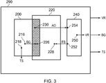
- Figure 3 is a schematic overview of the signal-generation circuitry 290 of Figure 2 , but with the circuit components removed for simplicity.
- the signal-generation circuitry 290 comprises the differential amplifier 220, bandgap reference circuitry 200, and regulation stage 240.
- the differential amplifier 220 and the bandgap reference circuitry 200 share some circuit components, namely those on the first current path. For example, there is a shared transistor 208. Indeed, recall that the first current-mirror transistor 204, the first input transistor 208 and the resistors 212 and 214 are common or shared between the bandgap reference circuitry 200 and the differential amplifier 220.
- the bandgap reference circuitry 200 produces its bandgap voltage reference signal (BG) at node 216 and its temperature-sensor signal (TS) at node 218.
- the differential amplifier 220 receives the bandgap voltage reference signal (BG) at node 226 and the feedback signal (FB) at node 228 as generated at node 252 by the regulation stage 240.
- the differential amplifier 220 outputs its amplifier output signal (AO) at node 230 based on a difference between the bandgap voltage reference signal (BG) and the feedback signal (FB).
- the regulation stage 240 receives the amplifier output signal (AO) at node 254 and generates the voltage-regulated signal (VR) at node 250 for use by external circuitry.
- the signal-generation circuitry 290 may output any or all of the voltage-regulated signal (VR), the bandgap voltage reference signal (BG) and the temperature-sensor signal (TS).
- the signal-generation circuitry 290 may be considered to be any or all of voltage regulator circuitry (or LDO circuitry), bandgap reference circuitry and temperature-sensor circuitry.
- the shared components in particular transistor 208, play a role in generating all three of these signals.
- the base terminal of the transistor 208 serves both as the reference node 216 at which the bandgap voltage reference signal is generated and as the first input terminal 226 of the differential amplifier 220.
- This transistor 208 is within the feedback loop formed using the differential amplifier 220.
- the common tail node 209 (the emitter terminal of the transistor 208) may also produce a temperature-sensor signal (TS).
- TS temperature-sensor signal
- the collector terminal of the transistor 208 forms node 230 at which the differential amplifier 220 outputs its amplifier output signal (AO).
- FIG. 4 is a schematic diagram of phase locked loop circuitry 400 which comprises the signal-generation circuitry 290.
- the phase locked loop (PLL) circuitry 400 comprises phase detector 410, loop filter 420, voltage controlled oscillator (VCO) 430, output node 440, feedback node 450, reference node 460 and the signal-generation circuitry 290.
- PLL phase locked loop
- the phase locked loop circuitry 400 is configured to output a signal at the output node 440 which has a desired frequency, by controlling that output signal relative to a reference signal input to the reference node 460 by means of negative feedback.
- the phase detector 410 in configured to detect a phase difference between the reference signal input to the reference node 460 and a feedback signal (which may be or be related to the output signal) input to the feedback node 450.
- the phase detector 410 outputs a signal generated to be proportional to the detected phase difference to the loop filter 420.
- the loop filter 420 is a low pass filter configured to filter high frequency signals from the phase detector output signal thereby generating a low frequency signal.
- the low frequency signal is input to the VCO 430.
- the VCO 430 is configured to generate a VCO signal as the output signal, having a frequency that is dependent on the magnitude of the low frequency signal received from the loop filter 420.
- the phase locked loop circuitry 400 is locked at a specific frequency when the feedback signal input to the feedback node 450 has the same phase angle as the reference signal input to the reference node 460.
- the phase detector 410 may comprise a charge pump at its output, to provide the output of the phase detector 410 as a current signal.
- a charge pump may operate based on a voltage-regulated reference signal (VR) output from the signal-generation circuitry 290, for example controlling one or more regulated current sources in that charge pump.
- VR voltage-regulated reference signal
- the signal-generation circuitry 290 may be employed in any of the blocks of the PLL, including the VCO 430.
- signal-generation circuitry 290 embodying the present invention could be provided as part of mixed-signal circuitry such as DAC or ADC circuitry 510, as illustrated in Figure 5 .
- circuitry disclosed herein could be described as an ADC or DAC, as just two convenient examples.
- the signal-generation circuitry disclosed herein can be used for any analogue or digital circuit that requires a regulated voltage supply.
- Circuitry of the present invention may be implemented as integrated circuitry, for example on an IC chip such as flip chip.
- the present invention extends to integrated circuitry and IC chips as mentioned above, circuit boards comprising such IC chips, and communication networks (for example, internet fiber-optic networks and wireless networks) and network equipment of such networks, comprising such circuit boards.
- BJTs may be replaced by FETs and vice versa.
- FETs field-effect transistors
Landscapes
- Engineering & Computer Science (AREA)
- Physics & Mathematics (AREA)
- Electromagnetism (AREA)
- General Physics & Mathematics (AREA)
- Radar, Positioning & Navigation (AREA)
- Automation & Control Theory (AREA)
- Microelectronics & Electronic Packaging (AREA)
- Power Engineering (AREA)
- Nonlinear Science (AREA)
- Control Of Electrical Variables (AREA)
Abstract
Description
- The present invention relates to signal-generation circuitry, for example for generating low-noise signals.
- Such a low-noise signal may be a voltage-regulated signal, which may be useful in phase locked loop (PLL) circuitry of analogue-to-digital or digital-to-analogue converter circuitry which is required to have a high degree of accuracy. Another example may be a temperature sensor signal. Another example may be a bandgap voltage signal.
- By way of background, conventional bandgap circuitry is used to generate a fixed and accurate reference voltage signal, i.e. whose voltage level is stable and independent of temperature. An output node of a bandgap circuit may be connected to external circuitry in order to provide the reference voltage signal to that external circuitry.
- Such a bandgap circuit unfortunately typically becomes unstable if significant current is drawn from the output node of the bandgap circuit e.g. by a resistive load. By connecting the output node to a resistive load, and thereby causing current to be drawn from that node, a typical bandgap circuit will malfunction. Consequently, typical bandgap circuits cannot be used to supply their reference voltage signals directly to current-drawing external circuity. The fixed reference voltage output by conventional bandgap circuitry is also difficult to increase above a certain value.
- However, such bandgap circuitry may be connected to low dropout (LDO) circuitry - or regulation circuitry - in order to provide a regulated reference voltage to a resistive load.
-
Figure 1 is a schematic diagram of previously-considered bandgap-regulator circuitry 180 comprising such LDO circuitry.Circuitry 180 comprises a reference-voltage generator 100 and anLDO output stage 140. - The
LDO output stage 140 comprises an operational amplifier (differential amplifier) 120, atransistor 142, afirst resistor 144, asecond resistor 146, acapacitor 148, aVDD voltage supply 160 and a ground (GND)voltage supply 170. Theoperational amplifier 120 has a firstoperational amplifier input 122, a secondoperational amplifier input 124, and anoperational amplifier output 126. - The reference-voltage generator 100 (which is a bandgap circuit) has a reference-voltage generator output node 102, and is configured to provide a fixed reference voltage signal (i.e. a bandgap voltage signal having a stable voltage level independent of temperature) at the reference-voltage generator output node 102. The reference-voltage generator output node 102 is connected to the first
operational amplifier input 122 such that the reference voltage signal is input to theoperational amplifier 120. - The
transistor 142 may be, for example, a PMOS MOSFET. In a case where thetransistor 142 is a PMOS MOSFET, the firstoperational amplifier input 122 is the inverting input and the secondoperational amplifier input 124 is the non-inverting input. - The
operational amplifier output 126 is connected to the gate terminal of thetransistor 142 of theLDO output stage 140, and thetransistor 142 is connected between thevoltage supply 160 and a bandgap-regulatorcircuitry output node 150, at which a regulated-reference voltage is to be supplied to the resistive load of external circuitry. - The first and
second resistors output node 150 and thevoltage supply 170 so as to form a potential divider. Afeedback node 152 is defined between thefirst resistor 144 and thesecond resistor 146, and is connected to the secondoperational amplifier input 124 so that a feedback voltage signal present at the feedback node is fed back to theoperational amplifier 120. - It will be appreciated that the LDO
output stage 140 operates to maintain or regulate the voltage level of the feedback voltage signal so that it is the same as that of the reference voltage signal. Any potential difference between those signals will cause a potential difference between the first and secondoperational amplifier inputs transistor 142 will thus be controlled to adjust the amount of current flowing through it to bring the voltage level of the feedback voltage signal back towards that of the reference voltage signal. This in turn regulates the voltage level of the signal provided at the bandgap-regulatorcircuitry output node 150 and thus provides the desired regulated reference voltage signal to the resistive load of the external circuitry in a form in which current can be drawn. Thus, the LDOoutput stage 140 acts as a non-inverting amplifier and buffer that supplies the required current to the load. - The
capacitor 148 is connected between the bandgap-regulatorcircuitry output node 150 and theground voltage supply 170 and is configured to filter high frequency noise from the regulated-reference voltage signal. - Despite the provision of such bandgap-
regulator circuitry 180, and the stability benefits afforded by theoperational amplifier 120 and theLDO output stage 140, it has been found that the previously-considered bandgap-regulator circuitry 180 suffers from problems such as noise and interference. - In particular, the
operational amplifier 120 serves as a noise contributor for the thermal noise floor. The input transistor pair (not shown) of theoperational amplifier 120 usually suffer from flicker noise as well. Further, if pluralLDO output stages 140 share the same reference-voltage generator 100, cross-talk and coupling can feed from oneLDO output stage 140 to another causing further noise performance degradation. - It is desirable to solve some or all of the above-mentioned problems.
- According to an embodiment of a first aspect of the present invention, there is provided signal-generation circuitry comprising: a differential amplifier comprising first and second (complementary) input transistors connected along first and second corresponding current paths, control terminals of the first and second input transistors serving as corresponding first and second input terminals of the differential amplifier, the differential amplifier having an output terminal at which an amplified signal is output dependent on first and second input signals received at the first and second input terminals, respectively; bandgap voltage reference circuitry also comprising said first current path having said first input transistor, the bandgap voltage reference circuitry further comprising a third current path having a third input transistor, wherein the control terminals of the first and third input transistors are connected together to form a reference terminal at which a bandgap voltage reference signal is generated as said first input signal; and a regulation stage connected to receive the amplified signal output from the differential amplifier and configured to generate a voltage-regulated signal based thereon, and connected to the second input terminal of the differential amplifier so that the second input signal is a feedback signal dependent on the voltage-regulated signal.
- Thus, there are shared components between the differential amplifier and the bandgap voltage reference circuitry, leading to improved noise performance. Further details of the associated advantages are provided later herein.
- The output terminal of the differential amplifier may be a node on the first current path.
- A capacitance may be connected between the output terminal and the reference terminal, to filter noise generated by the first and third input transistors at the reference terminal.
- The first and second input transistors are matched transistors, configured in the same way as one another. For example, they may have the same size or gain as one another.
- The first, second and third input transistors may be bipolar junction transistors, and the control terminals of those transistors may be base terminals of those transistors.
- The emitter terminals of the first and second input transistors may be connected together forming a common tail node at which the first and second current paths converge.
- The common tail node may be connected to the emitter terminal of the third input transistor via a first resistor, the first and second current paths passing from the common tail node through the first resistor. The emitter terminal of the third input transistor may be connected to a voltage reference source via a second resistor, the first, second and third current paths passing from the emitter terminal of the third input transistor through the second resistor.
- The first, second and third current paths may comprise first, second and third current-mirror transistors, respectively, connected together in a current-mirror arrangement configured to control currents flowing along the first and third current paths so that they are dependent on a current flowing along the second current path due to current mirroring.
- The first and third current-mirror transistors may have a size ratio 1:M and the first and third input transistors may have a size ratio N:1. In that case, the product of M and N should be greater than 1, where M and N are positive numbers (e.g. integers). The first and third current-mirror transistors may have a size ratio A:B and the first and third input transistors may have a size ratio C:D. In that case, the product of B and C should be greater than the product of A and D, where A, B, C and D are positive numbers (e.g. integers).
- The current-mirror transistors may be FETs, such as MOSFETs.
- The reference terminal of the bandgap voltage reference circuitry may be for providing a bandgap voltage reference signal to external circuitry, the signal-generation circuitry serving as a bandgap voltage reference source. Such signal-generation circuitry may have improved noise performance as compared to previously-considered bandgap voltage reference sources.
- The bandgap voltage reference circuitry may comprise a temperature-sensor node which provides a temperature-sensor voltage signal which is dependent on temperature, the signal-generation circuitry serving as a temperature sensor. Such signal-generation circuitry may have improved noise performance as compared to previously-considered temperature sensors.
- The regulation stage may be an output stage configured to provide the voltage-regulated signal as an output signal at an output terminal of the reference circuitry to power an external circuit, the signal-generation circuitry serving as a voltage regulator. Such signal-generation circuitry may have improved noise performance as compared to previously-considered voltage regulators.
- The regulation stage may comprise an output transistor connected to control a voltage at the output terminal in dependence upon the amplified signal. The output transistor may be connected to draw current from a voltage supply terminal.
- The regulation stage may comprise a potential divider connected to provide the feedback signal based on the voltage-regulated signal.
- According to an embodiment of a second aspect of the present invention, there is a provided phase locked loop circuit comprising the signal-generation circuitry according to the aforementioned first aspect of the present invention.
- According to an embodiment of a third aspect of the present invention, there is provided an integrated circuit such as an IC chip comprising the signal-generation circuitry according to the aforementioned first aspect of the present invention.
- Reference will now be made, by way of example, to the accompanying drawings, of which:
-
Figure 1 , considered above, is a schematic diagram of bandgap regulator circuitry; -
Figure 2 is a schematic diagram of signal-generation circuitry embodying the present invention; -
Figure 3 is another schematic diagram useful for understanding theFigure 2 circuitry; -
Figure 4 is a schematic diagram of phase locked loop circuitry which may comprise the signal-generation circuitry ofFigure 2 ; and -
Figure 5 is a schematic diagram of digital-to-analogue (DAC) circuitry or analogue-to-digital (ADC) circuitry which may comprise the signal-generation circuitry ofFigure 2 . -
Figure 2 is a schematic diagram of signal-generation circuitry 290 embodying the present invention. Signal-generation circuitry 290 comprises adifferential amplifier 220,bandgap reference circuitry 200, and aregulation stage 240. - In terms of general function, the
differential amplifier 220 may be compared with theoperational amplifier 120 ofFigure 1 , thebandgap reference circuitry 200 may be compared with the reference-voltage generator 100 ofFigure 1 , and theregulation stage 240 may be compared with the elements of theLDO output stage 140 ofFigure 1 other than theoperational amplifier 120. Thus, the general function of the signal-generation circuitry 290 corresponds to the general function of the bandgap-regulator circuitry 180. - However, the performance of the signal-
generation circuitry 290 is considered to exceed that of the bandgap-regulator circuitry 180 for various reasons, as will become apparent. - The
differential amplifier 220 comprises afirst input transistor 208, asecond input transistor 224, a first current-mirror transistor 204, a second current-mirror transistor 222, aresistor 212 and aresistor 214. - The
first input transistor 208 is connected along a first current path and thesecond input transistor 224 is connected along a second current path. The first andsecond input transistors common node 209 at which the first and second current paths converge. - The first and second current-
mirror transistors mirror transistor 204 is connected along the first current path between aVDD voltage supply 260 and the collector terminal of thefirst input transistor 208. Similarly the second current-mirror transistor 222 is connected along the second current path between theVDD voltage supply 260 and the collector terminal of thesecond input transistor 224. - The second current-
mirror transistor 222 is diode-connected whereby its gate terminal is connected to its drain terminal such that the second current-mirror transistor 222 is forced into the saturation region (some low-power arrangements could have the transistor in subthreshold rather than saturation). Further, the gate terminals of the first and second current-mirror transistors mirror transistors mirror arrangement 280 in which the current flowing in the first path through first current-mirror transistor 204 is related to the current flowing in the second path through the second current-mirror transistor 222 due to current mirroring. In the present case, the first and second current-mirror transistors - The
resistors common tail node 209 and a ground (GND)voltage supply 270, and define anode 218 between them. Thus, the first and second current paths pass in common through theresistors resistors - The
base terminals second input transistors differential amplifier 220, and correspond to the first and secondoperational amplifier inputs Figure 1 , respectively. Thecollector terminal 230 of thefirst input transistor 208 serves as theoutput terminal 230 of thedifferential amplifier 220, and corresponds to theoperational amplifier output 126 ofFigure 1 . - The
regulation stage 240 comprises output transistor (a PMOS MOSFET) 242, first and second potential-divider resistors output filter capacitor 248, connected in the same way as thetransistor 142, first andsecond resistors capacitor 148 ofFigure 1 , respectively. As an aside, theoutput transistor 242 could be implemented instead as anNMOS MOSFET 242 in which case the inputs to inputterminals - Thus, the
output terminal 230 of thedifferential amplifier 220 is connected to the gate terminal of thetransistor 242, which transistor is connected between theVDD voltage supply 260 and an output node 250 (corresponding to node 150), at which a regulated-reference voltage is to be supplied to the resistive load of external circuitry. - The first and second potential-
divider resistors output node 250 and the ground (GND)voltage supply 270 so as to form a potential divider. A feedback node 252 (corresponding to node 152) is defined between the first potential-divider resistor 244 and the second potential-divider resistor 246, and is connected to thesecond input terminal 228 of thedifferential amplifier 220 so that a feedback voltage signal present at thefeedback node 252 is fed back to thedifferential amplifier 220. - The
capacitor 148 is optional but preferred. - The
bandgap reference circuitry 200 provides a bandgap reference voltage signal at thefirst input terminal 226, in line with the reference-voltage generator 100. However, thebandgap reference circuitry 200 will be discussed in more detail later. - For now, it will be appreciated that the
differential amplifier 220 and regulation stage 240 (like the LDO output stage 140) operate to maintain or regulate the voltage level of the feedback voltage signal so that it is the same as that of the bandgap reference voltage signal. Any potential difference between those signals will cause a potential difference between the first andsecond input terminals differential amplifier 220, and thetransistor 242 will thus be controlled to adjust the amount of current flowing through it to bring the voltage level of the feedback voltage signal back towards that of the reference voltage signal. This in turn regulates the voltage level of the signal provided at theoutput node 250 and thus provides the desired regulated reference voltage signal to the resistive load of the external circuitry in a form in which current can be drawn by that load. - Thus, the
differential amplifier 220 and theregulation stage 240 together function as a LDO regulator circuit for generating the voltage-regulated signal. The voltage-regulated signal may be output to external circuitry such as, for example, phase locked loop (PLL) circuitry or indeed any circuitry (e.g. DACs and ADCs) that needs a voltage-regulated signal. The regulation function performed by thedifferential amplifier 220 and theregulation stage 240 serves to maintain a stable voltage-regulated signal (i.e. output voltage) even in a case where the voltage source used to supply power to the differential amplifier and the regulation stage operates at a voltage close to the desired voltage-regulated signal at the output node. - The
capacitor 248 is connected between theoutput node 250 and theground voltage supply 270 and is configured to filter high frequency noise from the regulated-reference voltage signal, thereby improving the signal-to-noise ratio (SNR) of the regulated-reference voltage signal which is output to external circuitry. - It is noted here that the first and second potential-
divider resistors output node 250 is higher than that of the bandgap reference voltage signal provided at thefirst input terminal 226. The difference between these voltage levels is of course dependent on the resistance values of the first and second potential-divider resistors divider resistors output node 250 itself. - Focus will now be placed on the
bandgap reference circuitry 200. - The
bandgap reference circuitry 200 comprises the first current-mirror transistor 204, thefirst input transistor 208, theresistors mirror transistor 202, and athird input transistor 206. Note in particular that the first current-mirror transistor 204, thefirst input transistor 208 and theresistors bandgap reference circuitry 200 and thedifferential amplifier 220. This leads to several advantages, as will be discussed later. - The third current-
mirror transistor 202 and thethird input transistor 206 are connected along a third current path which extends from thevoltage supply 260 through the third current-mirror transistor 202, through thethird input transistor 206 to thenode 218 where it passes through theresistor 214 to thevoltage supply 270. Thus, the first, second and third current paths converge at thenode 218 and pass through theresistor 214. - The third current-
mirror transistor 202 is a PMOS MOSFET comprising a gate terminal, a source terminal and a drain terminal. The gate terminal of the third current-mirror transistor 202 is connected to the gate terminals of the first and second current-mirror transistors mirror transistors mirror arrangement 280 in which the current flowing in the third path through the third current-mirror transistor 202 is related to the current flowing in the second path through the second current-mirror transistor 222 due to current mirroring. In the present case the third and second current-mirror transistors mirror transistors - The
third input transistor 206 is a BJT transistor, and itsbase terminal 210 is connected to thebase terminal 226 of thefirst input transistor 208, i.e. to thefirst input terminal 226 of thedifferential amplifier 220. This node (atterminals 210 and 226) may be referred to as areference node 216 at which the bandgap voltage reference signal is generated. The generation of the bandgap voltage reference signal is explained in detail below. Thebase terminal 210 is also connected to the collector terminal of thethird input transistor 206. - It will be recalled that the bandgap voltage reference signal generated at
reference node 216 serves as the voltage reference signal input to thedifferential amplifier 220. Acapacitor 211 is connected between thereference node 216 and the differentialamplifier output terminal 230. Thecapacitor 211 is configured to filter shot noise and/or thermal noise associated with the first andthird input transistors input capacitor 211 may be considered to comprise a combination of the discrete capacitor and the capacitance provided by the Miller effect in order to provide the total required capacitance for filtering shot noise. This capacitance may also act as the first dominant pole for the system. - The
reference node 216 may be connected to external circuitry such as a separateLDO output stage 140, thereby providing the bandgap voltage reference signal as an external reference signal. Due to noise filtering provided by thecapacitor 211, and the action of thedifferential amplifier 220, noise contributions from thefirst input transistor 208 and thethird input transistor 206 are attenuated in the bandgap voltage reference signal that would be output to external circuitry such that that bandgap voltage reference signal may be considered a low-noise bandgap voltage reference signal. - The generation of the bandgap voltage reference signal in the
bandgap reference circuitry 200 will now be explained. - The bandgap voltage reference signal generated at the
reference node 216 is a temperature-independent reference voltage signal whose voltage level is generated as a result of summing two potential differences which exhibit opposing temperature coefficients. These opposing temperature coefficients arise because the base-emitter voltages (Vbe) of thethird input transistor 206 and thefirst input transistor 208 of the bandgap reference circuitry 200 (being BJTs) both exhibit a negative temperature coefficient. - Different currents are generated in the first and third current paths, respectively. This is achieved by setting the size ratio M:1 between the third current-
mirror transistor 202 and the first current-mirror transistor 204, and the size ratio 1:N between thethird input transistor 206 and thefirst input transistor 208. Recall that the first andsecond input transistors third input transistors - It will become apparent that the two ratios may be set so that the product of M and N is greater than 1. Either M or N (but not both) may be 1. M may equal N as long as they are not equal to 1. M and N are both positive numbers, and may be integers. For example, if M = 1.5, the ratio M:1 may be expressed as 3:2. The present disclosure will be understood accordingly.
- In detail, the collector current of the
third input transistor 206 is given by: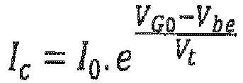
- The Vbe for the third input transistor 206 (the potential difference between
nodes 216 and 218) is given by:
- The derivative of Vbe with respect to temperature (7) is:

- Thus, Vbe for the
third input transistor 206 varies negatively with temperature - i.e. it exhibits a negative temperature coefficient. This relies on the negative temperature coefficient exhibited by the p-n junction corresponding to Vbe,206 in thethird input transistor 206. This negative temperature coefficient may be referred to as a Complementary To Absolute Temperature (CTAT) coefficient. - The difference ΔVbe between Vbe of the
third input transistor 206 and of the first input transistor 208 (the potential difference betweennodes 
- The current flowing through the
resistor 212 is given by:


- The voltage across the
resistor 214 is thus given by:
- The derivative of V214 with respect to temperature (T) is given by:

- Thus, the voltage V214 across the
resistor 214 varies positively with temperature - i.e. it exhibits a positive temperature coefficient. This relies on the positive temperature coefficient exhibited by the difference between the p-n junctions corresponding to Vbe in the first andthird input transistors - The summing together of V214 and Vbe,206, as defined above, results in the bandgap voltage reference signal being generated at the
reference node 216. The parameters of M, N, R 212 and R 214 may be tuned or selected in order to minimise variation in the bandgap voltage reference signal across a required temperature range, so that over that temperature range the bandgap voltage reference signal may be considered temperature-independent. Temperature independence will be understood as such herein. - It is noted as an aside that the
resistors tail node 209 of thedifferential amplifier 220, where the common mode gain of the differential amplifier is inversely proportional to the resistance of the resistive current source, and the common mode rejection ratio (CMRR) is directly proportional to the resistance of the resistive current source. From the equations above, the resistances of these tworesistors - The bandgap voltage reference signal may be generated to be between 1.2V and 1.3V thereby generating a temperature independent voltage close to the theoretical 1.22 eV bandgap of silicon at 0K.
- Note that the voltage level of a signal at
node 218 varies positively with temperature since V214 varies positively with temperature and theground supply voltage 270 is considered to be stable with temperature. Thus, by using that signal as an output signal the signal-generation circuitry 290 could be described as a temperature sensor.Node 218 may also be described as a temperature-sensor node 218. By connecting the temperature-sensor node 218 to external circuitry the signal atnode 218 may be used as a temperature-dependent reference voltage signal. - Due to the
first input transistor 208 and the first current-mirror transistor 204 being incorporated into the feedback loop of thedifferential amplifier 220, noise contribution from thefirst input transistor 208 and the first current-mirror transistor 204 is divided by the feedback loop gain of thedifferential amplifier 220, which thereby reduces noise experienced by the temperature dependent voltage signal atnode 218 and the amplified signal output from thedifferential amplifier 220 atnode 230. This of course reduces noise experienced in the regulated reference voltage signal at theoutput node 250. Moreover, the noise contribution from thefirst input transistor 208, the third current-mirror transistor 202 and thethird input transistor 206 is filtered by thecapacitor 211, which further reduces noise experienced in these signals. - Advantageously, by reducing the number of devices required to generate a voltage-regulated signal due to the shared circuitry, compared to for example in the
Figure 1 circuitry where there is no sharing of components in the sense ofFigure 2 , the overall noise contribution of the signal-generation circuitry 290 is reduced. - Advantageously, the voltage-regulated signal generated at the
output node 250 may be considered temperature-independent over the temperature range mentioned above, in the same way as the bandgap voltage reference signal may be. Theoutput node 250 may be connected to external circuitry such that the temperature independent voltage-regulated signal is provided to the external circuitry as a regulated-reference signal. - Furthermore, since the signal-
generation circuitry 290 performs the function of generating a bandgap voltage reference signal and the related voltage-regulated signal within a single combined circuit, the problem of cross talk and coupling between the reference-voltage generator 100 and multiple LDO output stages 140 is eliminated, since instead multiple instances of the signal-generation circuitry 290 would be provided. Advantageously, each instance of the signal-generation circuitry 290 includes thebandgap reference circuitry 200 and theregulation stage 240 in the same circuit thereby providing its own separate bandgap voltage reference signal and related voltage-regulated signal. - Incidentally, it will be appreciated that the
Figure 2 circuitry could be adapted to be the other way up, swapping n-channel devices for p-channel devices and similar. In that event, however, the bandgap voltage would be relative to supply (VDD) rather than relative to ground (GND), which may be less preferable in general. - By way of summary,
Figure 3 is a schematic overview of the signal-generation circuitry 290 ofFigure 2 , but with the circuit components removed for simplicity. As before, the signal-generation circuitry 290 comprises thedifferential amplifier 220,bandgap reference circuitry 200, andregulation stage 240. - As can be seen schematically by virtue of the shaded overlap, the
differential amplifier 220 and thebandgap reference circuitry 200 share some circuit components, namely those on the first current path. For example, there is a sharedtransistor 208. Indeed, recall that the first current-mirror transistor 204, thefirst input transistor 208 and theresistors bandgap reference circuitry 200 and thedifferential amplifier 220. - The
bandgap reference circuitry 200 produces its bandgap voltage reference signal (BG) atnode 216 and its temperature-sensor signal (TS) atnode 218. Thedifferential amplifier 220 receives the bandgap voltage reference signal (BG) atnode 226 and the feedback signal (FB) atnode 228 as generated atnode 252 by theregulation stage 240. Thedifferential amplifier 220 outputs its amplifier output signal (AO) atnode 230 based on a difference between the bandgap voltage reference signal (BG) and the feedback signal (FB). Theregulation stage 240 receives the amplifier output signal (AO) atnode 254 and generates the voltage-regulated signal (VR) atnode 250 for use by external circuitry. - As indicated, the signal-
generation circuitry 290 may output any or all of the voltage-regulated signal (VR), the bandgap voltage reference signal (BG) and the temperature-sensor signal (TS). Thus, the signal-generation circuitry 290 may be considered to be any or all of voltage regulator circuitry (or LDO circuitry), bandgap reference circuitry and temperature-sensor circuitry. - Note that the shared components, in
particular transistor 208, play a role in generating all three of these signals. For example, the base terminal of thetransistor 208 serves both as thereference node 216 at which the bandgap voltage reference signal is generated and as thefirst input terminal 226 of thedifferential amplifier 220. Thistransistor 208 is within the feedback loop formed using thedifferential amplifier 220. Note that the common tail node 209 (the emitter terminal of the transistor 208) may also produce a temperature-sensor signal (TS). Note also that the collector terminal of thetransistor 208forms node 230 at which thedifferential amplifier 220 outputs its amplifier output signal (AO). - By taking advantage of the particular and shared circuit topologies of the
bandgap reference circuitry 200 and thedifferential amplifier 220, a single sharedtransistor 208 is used to perform multiple functions. By way of contrast, such advantages do not stem from the circuitry ofFigure 1 , where there is no such overlap/integration between the reference-voltage generator 100 and theLDO output stage 140. -
Figure 4 is a schematic diagram of phase lockedloop circuitry 400 which comprises the signal-generation circuitry 290. The phase locked loop (PLL)circuitry 400 comprisesphase detector 410,loop filter 420, voltage controlled oscillator (VCO) 430,output node 440,feedback node 450,reference node 460 and the signal-generation circuitry 290. - The phase locked
loop circuitry 400 is configured to output a signal at theoutput node 440 which has a desired frequency, by controlling that output signal relative to a reference signal input to thereference node 460 by means of negative feedback. - The
phase detector 410 in configured to detect a phase difference between the reference signal input to thereference node 460 and a feedback signal (which may be or be related to the output signal) input to thefeedback node 450. Thephase detector 410 outputs a signal generated to be proportional to the detected phase difference to theloop filter 420. Theloop filter 420 is a low pass filter configured to filter high frequency signals from the phase detector output signal thereby generating a low frequency signal. The low frequency signal is input to theVCO 430. TheVCO 430 is configured to generate a VCO signal as the output signal, having a frequency that is dependent on the magnitude of the low frequency signal received from theloop filter 420. - The phase locked
loop circuitry 400 is locked at a specific frequency when the feedback signal input to thefeedback node 450 has the same phase angle as the reference signal input to thereference node 460. - The
phase detector 410 may comprise a charge pump at its output, to provide the output of thephase detector 410 as a current signal. Such a charge pump may operate based on a voltage-regulated reference signal (VR) output from the signal-generation circuitry 290, for example controlling one or more regulated current sources in that charge pump. Of course, the signal-generation circuitry 290 may be employed in any of the blocks of the PLL, including theVCO 430. - It will be appreciated that the signal-
generation circuitry 290 embodying the present invention (perhaps provided within a PLL generating clock signals)) could be provided as part of mixed-signal circuitry such as DAC orADC circuitry 510, as illustrated inFigure 5 . - It will be appreciated therefore that circuitry disclosed herein could be described as an ADC or DAC, as just two convenient examples. In general, the signal-generation circuitry disclosed herein can be used for any analogue or digital circuit that requires a regulated voltage supply.
- Circuitry of the present invention may be implemented as integrated circuitry, for example on an IC chip such as flip chip. The present invention extends to integrated circuitry and IC chips as mentioned above, circuit boards comprising such IC chips, and communication networks (for example, internet fiber-optic networks and wireless networks) and network equipment of such networks, comprising such circuit boards.
- It will be appreciated that BJTs may be replaced by FETs and vice versa. The present disclosure will be understood accordingly.
- The present invention may be embodied in many different ways in the light of the above disclosure, within the spirit and scope of the appended claims.
Claims (15)
- Signal-generation circuitry comprising:a differential amplifier comprising first and second input transistors connected along first and second corresponding current paths, control terminals of the first and second input transistors serving as corresponding first and second input terminals of the differential amplifier, the differential amplifier having an output terminal at which an amplified signal is output dependent on first and second input signals received at the first and second input terminals, respectively;bandgap voltage reference circuitry also comprising said first current path having said first input transistor, the bandgap voltage reference circuitry further comprising a third current path having a third input transistor, wherein the control terminals of the first and third input transistors are connected together to form a reference terminal at which a bandgap voltage reference signal is generated as said first input signal; anda regulation stage connected to receive the amplified signal output from the differential amplifier and configured to generate a voltage-regulated signal based thereon, and connected to the second input terminal of the differential amplifier so that the second input signal is a feedback signal dependent on the voltage-regulated signal.
- The signal-generation circuitry according to claim 1, wherein the output terminal of the differential amplifier is a node on the first current path.
- The signal-generation circuitry according to claim 1 or 2, wherein a capacitance is connected between the output terminal and the reference terminal, to filter noise generated by the first and third input transistors at the reference terminal.
- The signal-generation circuitry according to any of the preceding claims, wherein the first and second input transistors are matched transistors, configured in the same way as one another.
- The signal-generation circuitry according to any of the preceding claims, wherein the first, second and third input transistors are bipolar junction transistors, and the control terminals of those transistors are base terminals of those transistors.
- The signal-generation circuitry according to claim 5, wherein the emitter terminals of the first and second input transistors are connected together forming a common tail node at which the first and second current paths converge.
- The signal-generation circuitry according to claim 6, wherein the common tail node is connected to the emitter terminal of the third input transistor via a first resistor, the first and second current paths passing from the common tail node through the first resistor, and wherein the emitter terminal of the third input transistor is connected to a voltage reference source via a second resistor, the first, second and third current paths passing from the emitter terminal of the third input transistor through the second resistor.
- The signal-generation circuitry according to any of the preceding claims, wherein the first, second and third current paths comprise first, second and third current-mirror transistors, respectively, connected together in a current-mirror arrangement configured to control currents flowing along the first and third current paths so that they are dependent on a current flowing along the second current path due to current mirroring.
- The signal-generation circuitry according to claim 8, wherein:the first and third current-mirror transistors have a size ratio 1:M and wherein the first and third input transistors have a size ratio N:1, and wherein the product of M and N is greater than 1, where M and N are positive numbers; orthe first and third current-mirror transistors have a size ratio A:B and wherein the first and third input transistors have a size ratio C:D, and wherein the product of B and C is greater than the product of A and D, where A, B, C and D are positive numbers.
- The signal-generation circuitry according to claim 8 or 9, wherein the current-mirror transistors are FETs.
- The signal-generation circuitry according to any of the preceding claims, wherein the reference terminal of the bandgap voltage reference circuitry is for providing a bandgap voltage reference signal to external circuitry, the signal-generation circuitry serving as a bandgap voltage reference source.
- The signal-generation circuitry according to any of the preceding claims, wherein the bandgap voltage reference circuitry comprises a temperature-sensor node which provides a temperature-sensor voltage signal which is dependent on temperature, the signal-generation circuitry serving as a temperature sensor.
- The signal-generation circuitry according to any of the preceding claims, wherein the regulation stage is an output stage configured to provide the voltage-regulated signal as an output signal at an output terminal of the reference circuitry to power an external circuit, the signal-generation circuitry serving as a voltage regulator.
- The signal-generation circuitry according to claim 13, wherein the regulation stage comprises an output transistor connected to control a voltage at the output terminal in dependence upon the amplified signal.
- An integrated circuit such as an IC chip comprising the signal-generation circuitry as claimed in any of the preceding claims.
Priority Applications (2)
| Application Number | Priority Date | Filing Date | Title |
|---|---|---|---|
| EP18152588.2A EP3514653B1 (en) | 2018-01-19 | 2018-01-19 | Signal-generation circuitry |
| US16/244,016 US10671104B2 (en) | 2018-01-19 | 2019-01-09 | Signal generation circuitry |
Applications Claiming Priority (1)
| Application Number | Priority Date | Filing Date | Title |
|---|---|---|---|
| EP18152588.2A EP3514653B1 (en) | 2018-01-19 | 2018-01-19 | Signal-generation circuitry |
Publications (2)
| Publication Number | Publication Date |
|---|---|
| EP3514653A1 true EP3514653A1 (en) | 2019-07-24 |
| EP3514653B1 EP3514653B1 (en) | 2022-06-08 |
Family
ID=61007608
Family Applications (1)
| Application Number | Title | Priority Date | Filing Date |
|---|---|---|---|
| EP18152588.2A Active EP3514653B1 (en) | 2018-01-19 | 2018-01-19 | Signal-generation circuitry |
Country Status (2)
| Country | Link |
|---|---|
| US (1) | US10671104B2 (en) |
| EP (1) | EP3514653B1 (en) |
Families Citing this family (6)
| Publication number | Priority date | Publication date | Assignee | Title |
|---|---|---|---|---|
| JP2020135372A (en) * | 2019-02-19 | 2020-08-31 | ローム株式会社 | Power supply circuit |
| JP2021144411A (en) | 2020-03-11 | 2021-09-24 | キオクシア株式会社 | Semiconductor device and memory system |
| EP3951551B1 (en) * | 2020-08-07 | 2023-02-22 | Scalinx | Voltage regulator and method |
| JP7678287B2 (en) * | 2021-05-28 | 2025-05-16 | ミツミ電機株式会社 | Semiconductor Integrated Circuit |
| US11869603B2 (en) * | 2021-08-13 | 2024-01-09 | Micron Technology, Inc. | Voltage regulation |
| KR20240163384A (en) | 2023-05-10 | 2024-11-19 | 에스케이하이닉스 주식회사 | Voltage generator and clock generating circuit including the same |
Citations (3)
| Publication number | Priority date | Publication date | Assignee | Title |
|---|---|---|---|---|
| US20090302823A1 (en) * | 2008-06-10 | 2009-12-10 | Analog Devices, Inc. | Voltage regulator circuit |
| EP2804067A1 (en) * | 2013-05-17 | 2014-11-19 | Asahi Kasei Microdevices Corporation | Low output noise density low power ldo voltage regulator |
| EP2977849A1 (en) * | 2014-07-24 | 2016-01-27 | Dialog Semiconductor GmbH | High-voltage to low-voltage low dropout regulator with self contained voltage reference |
Family Cites Families (4)
| Publication number | Priority date | Publication date | Assignee | Title |
|---|---|---|---|---|
| US5861736A (en) | 1994-12-01 | 1999-01-19 | Texas Instruments Incorporated | Circuit and method for regulating a voltage |
| US6271652B1 (en) * | 2000-09-29 | 2001-08-07 | International Business Machines Corporation | Voltage regulator with gain boosting |
| US7602162B2 (en) | 2005-11-29 | 2009-10-13 | Stmicroelectronics Pvt. Ltd. | Voltage regulator with over-current protection |
| US9970826B2 (en) * | 2015-03-04 | 2018-05-15 | Qualcomm Incorporated | Bipolar junction transistor voltage-drop-based temperature sensors |
-
2018
- 2018-01-19 EP EP18152588.2A patent/EP3514653B1/en active Active
-
2019
- 2019-01-09 US US16/244,016 patent/US10671104B2/en active Active
Patent Citations (3)
| Publication number | Priority date | Publication date | Assignee | Title |
|---|---|---|---|---|
| US20090302823A1 (en) * | 2008-06-10 | 2009-12-10 | Analog Devices, Inc. | Voltage regulator circuit |
| EP2804067A1 (en) * | 2013-05-17 | 2014-11-19 | Asahi Kasei Microdevices Corporation | Low output noise density low power ldo voltage regulator |
| EP2977849A1 (en) * | 2014-07-24 | 2016-01-27 | Dialog Semiconductor GmbH | High-voltage to low-voltage low dropout regulator with self contained voltage reference |
Also Published As
| Publication number | Publication date |
|---|---|
| EP3514653B1 (en) | 2022-06-08 |
| US20190227587A1 (en) | 2019-07-25 |
| US10671104B2 (en) | 2020-06-02 |
Similar Documents
| Publication | Publication Date | Title |
|---|---|---|
| US10671104B2 (en) | Signal generation circuitry | |
| US10198022B1 (en) | Ultra-low power bias current generation and utilization in current and voltage source and regulator devices | |
| US7656145B2 (en) | Low power bandgap voltage reference circuit having multiple reference voltages with high power supply rejection ratio | |
| TWI459174B (en) | Low noise voltage reference circuit | |
| US9785176B2 (en) | Small-circuit-scale reference voltage generating circuit | |
| US11474552B2 (en) | Voltage reference temperature compensation circuits and methods | |
| US7078958B2 (en) | CMOS bandgap reference with low voltage operation | |
| JP6242274B2 (en) | Band gap reference circuit and semiconductor device including the same | |
| US9740229B2 (en) | Curvature-corrected bandgap reference | |
| US20090302823A1 (en) | Voltage regulator circuit | |
| US20150331439A1 (en) | Electronic Device and Method for Generating a Curvature Compensated Bandgap Reference Voltage | |
| CN102369495A (en) | Method and circuit for low power voltage reference and bias current generator | |
| CN110895423B (en) | System and method for proportional to absolute temperature circuit | |
| KR100721736B1 (en) | Constant-current circuit and system power source using this constant-current circuit | |
| US6680643B2 (en) | Bandgap type reference voltage source with low supply voltage | |
| US20120319793A1 (en) | Oscillation circuit | |
| US9098098B2 (en) | Curvature-corrected bandgap reference | |
| US20190324491A1 (en) | Bandgap Reference Circuit and Method for Providing a Reference Voltage | |
| US20070080740A1 (en) | Reference circuit for providing a temperature independent reference voltage and current | |
| US8884601B2 (en) | System and method for a low voltage bandgap reference | |
| EP2804067B1 (en) | Low output noise density low power ldo voltage regulator | |
| US6215353B1 (en) | Stable voltage reference circuit | |
| US20110267133A1 (en) | Current generating circuit | |
| JP6413005B2 (en) | Semiconductor device and electronic system | |
| US9304528B2 (en) | Reference voltage generator with op-amp buffer |
Legal Events
| Date | Code | Title | Description |
|---|---|---|---|
| PUAI | Public reference made under article 153(3) epc to a published international application that has entered the european phase |
Free format text: ORIGINAL CODE: 0009012 |
|
| STAA | Information on the status of an ep patent application or granted ep patent |
Free format text: STATUS: THE APPLICATION HAS BEEN PUBLISHED |
|
| AK | Designated contracting states |
Kind code of ref document: A1 Designated state(s): AL AT BE BG CH CY CZ DE DK EE ES FI FR GB GR HR HU IE IS IT LI LT LU LV MC MK MT NL NO PL PT RO RS SE SI SK SM TR |
|
| AX | Request for extension of the european patent |
Extension state: BA ME |
|
| STAA | Information on the status of an ep patent application or granted ep patent |
Free format text: STATUS: REQUEST FOR EXAMINATION WAS MADE |
|
| 17P | Request for examination filed |
Effective date: 20200114 |
|
| RBV | Designated contracting states (corrected) |
Designated state(s): AL AT BE BG CH CY CZ DE DK EE ES FI FR GB GR HR HU IE IS IT LI LT LU LV MC MK MT NL NO PL PT RO RS SE SI SK SM TR |
|
| STAA | Information on the status of an ep patent application or granted ep patent |
Free format text: STATUS: EXAMINATION IS IN PROGRESS |
|
| 17Q | First examination report despatched |
Effective date: 20210225 |
|
| GRAJ | Information related to disapproval of communication of intention to grant by the applicant or resumption of examination proceedings by the epo deleted |
Free format text: ORIGINAL CODE: EPIDOSDIGR1 |
|
| STAA | Information on the status of an ep patent application or granted ep patent |
Free format text: STATUS: GRANT OF PATENT IS INTENDED |
|
| GRAP | Despatch of communication of intention to grant a patent |
Free format text: ORIGINAL CODE: EPIDOSNIGR1 |
|
| INTG | Intention to grant announced |
Effective date: 20220105 |
|
| GRAS | Grant fee paid |
Free format text: ORIGINAL CODE: EPIDOSNIGR3 |
|
| GRAA | (expected) grant |
Free format text: ORIGINAL CODE: 0009210 |
|
| STAA | Information on the status of an ep patent application or granted ep patent |
Free format text: STATUS: THE PATENT HAS BEEN GRANTED |
|
| AK | Designated contracting states |
Kind code of ref document: B1 Designated state(s): AL AT BE BG CH CY CZ DE DK EE ES FI FR GB GR HR HU IE IS IT LI LT LU LV MC MK MT NL NO PL PT RO RS SE SI SK SM TR |
|
| REG | Reference to a national code |
Ref country code: AT Ref legal event code: REF Ref document number: 1497366 Country of ref document: AT Kind code of ref document: T Effective date: 20220615 Ref country code: CH Ref legal event code: EP |
|
| REG | Reference to a national code |
Ref country code: DE Ref legal event code: R096 Ref document number: 602018036391 Country of ref document: DE |
|
| REG | Reference to a national code |
Ref country code: IE Ref legal event code: FG4D |
|
| REG | Reference to a national code |
Ref country code: LT Ref legal event code: MG9D |
|
| REG | Reference to a national code |
Ref country code: NL Ref legal event code: MP Effective date: 20220608 |
|
| PG25 | Lapsed in a contracting state [announced via postgrant information from national office to epo] |
Ref country code: SE Free format text: LAPSE BECAUSE OF FAILURE TO SUBMIT A TRANSLATION OF THE DESCRIPTION OR TO PAY THE FEE WITHIN THE PRESCRIBED TIME-LIMIT Effective date: 20220608 Ref country code: NO Free format text: LAPSE BECAUSE OF FAILURE TO SUBMIT A TRANSLATION OF THE DESCRIPTION OR TO PAY THE FEE WITHIN THE PRESCRIBED TIME-LIMIT Effective date: 20220908 Ref country code: LT Free format text: LAPSE BECAUSE OF FAILURE TO SUBMIT A TRANSLATION OF THE DESCRIPTION OR TO PAY THE FEE WITHIN THE PRESCRIBED TIME-LIMIT Effective date: 20220608 Ref country code: HR Free format text: LAPSE BECAUSE OF FAILURE TO SUBMIT A TRANSLATION OF THE DESCRIPTION OR TO PAY THE FEE WITHIN THE PRESCRIBED TIME-LIMIT Effective date: 20220608 Ref country code: GR Free format text: LAPSE BECAUSE OF FAILURE TO SUBMIT A TRANSLATION OF THE DESCRIPTION OR TO PAY THE FEE WITHIN THE PRESCRIBED TIME-LIMIT Effective date: 20220909 Ref country code: FI Free format text: LAPSE BECAUSE OF FAILURE TO SUBMIT A TRANSLATION OF THE DESCRIPTION OR TO PAY THE FEE WITHIN THE PRESCRIBED TIME-LIMIT Effective date: 20220608 Ref country code: ES Free format text: LAPSE BECAUSE OF FAILURE TO SUBMIT A TRANSLATION OF THE DESCRIPTION OR TO PAY THE FEE WITHIN THE PRESCRIBED TIME-LIMIT Effective date: 20220608 Ref country code: BG Free format text: LAPSE BECAUSE OF FAILURE TO SUBMIT A TRANSLATION OF THE DESCRIPTION OR TO PAY THE FEE WITHIN THE PRESCRIBED TIME-LIMIT Effective date: 20220908 |
|
| REG | Reference to a national code |
Ref country code: AT Ref legal event code: MK05 Ref document number: 1497366 Country of ref document: AT Kind code of ref document: T Effective date: 20220608 |
|
| PG25 | Lapsed in a contracting state [announced via postgrant information from national office to epo] |
Ref country code: RS Free format text: LAPSE BECAUSE OF FAILURE TO SUBMIT A TRANSLATION OF THE DESCRIPTION OR TO PAY THE FEE WITHIN THE PRESCRIBED TIME-LIMIT Effective date: 20220608 Ref country code: LV Free format text: LAPSE BECAUSE OF FAILURE TO SUBMIT A TRANSLATION OF THE DESCRIPTION OR TO PAY THE FEE WITHIN THE PRESCRIBED TIME-LIMIT Effective date: 20220608 |
|
| PG25 | Lapsed in a contracting state [announced via postgrant information from national office to epo] |
Ref country code: NL Free format text: LAPSE BECAUSE OF FAILURE TO SUBMIT A TRANSLATION OF THE DESCRIPTION OR TO PAY THE FEE WITHIN THE PRESCRIBED TIME-LIMIT Effective date: 20220608 |
|
| PG25 | Lapsed in a contracting state [announced via postgrant information from national office to epo] |
Ref country code: SM Free format text: LAPSE BECAUSE OF FAILURE TO SUBMIT A TRANSLATION OF THE DESCRIPTION OR TO PAY THE FEE WITHIN THE PRESCRIBED TIME-LIMIT Effective date: 20220608 Ref country code: SK Free format text: LAPSE BECAUSE OF FAILURE TO SUBMIT A TRANSLATION OF THE DESCRIPTION OR TO PAY THE FEE WITHIN THE PRESCRIBED TIME-LIMIT Effective date: 20220608 Ref country code: RO Free format text: LAPSE BECAUSE OF FAILURE TO SUBMIT A TRANSLATION OF THE DESCRIPTION OR TO PAY THE FEE WITHIN THE PRESCRIBED TIME-LIMIT Effective date: 20220608 Ref country code: PT Free format text: LAPSE BECAUSE OF FAILURE TO SUBMIT A TRANSLATION OF THE DESCRIPTION OR TO PAY THE FEE WITHIN THE PRESCRIBED TIME-LIMIT Effective date: 20221010 Ref country code: EE Free format text: LAPSE BECAUSE OF FAILURE TO SUBMIT A TRANSLATION OF THE DESCRIPTION OR TO PAY THE FEE WITHIN THE PRESCRIBED TIME-LIMIT Effective date: 20220608 Ref country code: CZ Free format text: LAPSE BECAUSE OF FAILURE TO SUBMIT A TRANSLATION OF THE DESCRIPTION OR TO PAY THE FEE WITHIN THE PRESCRIBED TIME-LIMIT Effective date: 20220608 Ref country code: AT Free format text: LAPSE BECAUSE OF FAILURE TO SUBMIT A TRANSLATION OF THE DESCRIPTION OR TO PAY THE FEE WITHIN THE PRESCRIBED TIME-LIMIT Effective date: 20220608 |
|
| PG25 | Lapsed in a contracting state [announced via postgrant information from national office to epo] |
Ref country code: PL Free format text: LAPSE BECAUSE OF FAILURE TO SUBMIT A TRANSLATION OF THE DESCRIPTION OR TO PAY THE FEE WITHIN THE PRESCRIBED TIME-LIMIT Effective date: 20220608 Ref country code: IS Free format text: LAPSE BECAUSE OF FAILURE TO SUBMIT A TRANSLATION OF THE DESCRIPTION OR TO PAY THE FEE WITHIN THE PRESCRIBED TIME-LIMIT Effective date: 20221008 |
|
| REG | Reference to a national code |
Ref country code: DE Ref legal event code: R097 Ref document number: 602018036391 Country of ref document: DE |
|
| PG25 | Lapsed in a contracting state [announced via postgrant information from national office to epo] |
Ref country code: AL Free format text: LAPSE BECAUSE OF FAILURE TO SUBMIT A TRANSLATION OF THE DESCRIPTION OR TO PAY THE FEE WITHIN THE PRESCRIBED TIME-LIMIT Effective date: 20220608 |
|
| PLBE | No opposition filed within time limit |
Free format text: ORIGINAL CODE: 0009261 |
|
| STAA | Information on the status of an ep patent application or granted ep patent |
Free format text: STATUS: NO OPPOSITION FILED WITHIN TIME LIMIT |
|
| PG25 | Lapsed in a contracting state [announced via postgrant information from national office to epo] |
Ref country code: DK Free format text: LAPSE BECAUSE OF FAILURE TO SUBMIT A TRANSLATION OF THE DESCRIPTION OR TO PAY THE FEE WITHIN THE PRESCRIBED TIME-LIMIT Effective date: 20220608 |
|
| 26N | No opposition filed |
Effective date: 20230310 |
|
| PG25 | Lapsed in a contracting state [announced via postgrant information from national office to epo] |
Ref country code: SI Free format text: LAPSE BECAUSE OF FAILURE TO SUBMIT A TRANSLATION OF THE DESCRIPTION OR TO PAY THE FEE WITHIN THE PRESCRIBED TIME-LIMIT Effective date: 20220608 |
|
| REG | Reference to a national code |
Ref country code: CH Ref legal event code: PL |
|
| GBPC | Gb: european patent ceased through non-payment of renewal fee |
Effective date: 20230119 |
|
| PG25 | Lapsed in a contracting state [announced via postgrant information from national office to epo] |
Ref country code: LU Free format text: LAPSE BECAUSE OF NON-PAYMENT OF DUE FEES Effective date: 20230119 |
|
| REG | Reference to a national code |
Ref country code: BE Ref legal event code: MM Effective date: 20230131 |
|
| PG25 | Lapsed in a contracting state [announced via postgrant information from national office to epo] |
Ref country code: LI Free format text: LAPSE BECAUSE OF NON-PAYMENT OF DUE FEES Effective date: 20230131 Ref country code: GB Free format text: LAPSE BECAUSE OF NON-PAYMENT OF DUE FEES Effective date: 20230119 Ref country code: CH Free format text: LAPSE BECAUSE OF NON-PAYMENT OF DUE FEES Effective date: 20230131 |
|
| PG25 | Lapsed in a contracting state [announced via postgrant information from national office to epo] |
Ref country code: FR Free format text: LAPSE BECAUSE OF NON-PAYMENT OF DUE FEES Effective date: 20230131 Ref country code: BE Free format text: LAPSE BECAUSE OF NON-PAYMENT OF DUE FEES Effective date: 20230131 |
|
| PG25 | Lapsed in a contracting state [announced via postgrant information from national office to epo] |
Ref country code: IT Free format text: LAPSE BECAUSE OF FAILURE TO SUBMIT A TRANSLATION OF THE DESCRIPTION OR TO PAY THE FEE WITHIN THE PRESCRIBED TIME-LIMIT Effective date: 20220608 Ref country code: IE Free format text: LAPSE BECAUSE OF NON-PAYMENT OF DUE FEES Effective date: 20230119 |
|
| PG25 | Lapsed in a contracting state [announced via postgrant information from national office to epo] |
Ref country code: MC Free format text: LAPSE BECAUSE OF FAILURE TO SUBMIT A TRANSLATION OF THE DESCRIPTION OR TO PAY THE FEE WITHIN THE PRESCRIBED TIME-LIMIT Effective date: 20220608 |
|
| PG25 | Lapsed in a contracting state [announced via postgrant information from national office to epo] |
Ref country code: MC Free format text: LAPSE BECAUSE OF FAILURE TO SUBMIT A TRANSLATION OF THE DESCRIPTION OR TO PAY THE FEE WITHIN THE PRESCRIBED TIME-LIMIT Effective date: 20220608 |
|
| PG25 | Lapsed in a contracting state [announced via postgrant information from national office to epo] |
Ref country code: BG Free format text: LAPSE BECAUSE OF FAILURE TO SUBMIT A TRANSLATION OF THE DESCRIPTION OR TO PAY THE FEE WITHIN THE PRESCRIBED TIME-LIMIT Effective date: 20220608 |
|
| PG25 | Lapsed in a contracting state [announced via postgrant information from national office to epo] |
Ref country code: BG Free format text: LAPSE BECAUSE OF FAILURE TO SUBMIT A TRANSLATION OF THE DESCRIPTION OR TO PAY THE FEE WITHIN THE PRESCRIBED TIME-LIMIT Effective date: 20220608 |
|
| PG25 | Lapsed in a contracting state [announced via postgrant information from national office to epo] |
Ref country code: CY Free format text: LAPSE BECAUSE OF FAILURE TO SUBMIT A TRANSLATION OF THE DESCRIPTION OR TO PAY THE FEE WITHIN THE PRESCRIBED TIME-LIMIT; INVALID AB INITIO Effective date: 20180119 |
|
| PG25 | Lapsed in a contracting state [announced via postgrant information from national office to epo] |
Ref country code: HU Free format text: LAPSE BECAUSE OF FAILURE TO SUBMIT A TRANSLATION OF THE DESCRIPTION OR TO PAY THE FEE WITHIN THE PRESCRIBED TIME-LIMIT; INVALID AB INITIO Effective date: 20180119 |
|
| PG25 | Lapsed in a contracting state [announced via postgrant information from national office to epo] |
Ref country code: TR Free format text: LAPSE BECAUSE OF FAILURE TO SUBMIT A TRANSLATION OF THE DESCRIPTION OR TO PAY THE FEE WITHIN THE PRESCRIBED TIME-LIMIT Effective date: 20220608 |
|
| PGFP | Annual fee paid to national office [announced via postgrant information from national office to epo] |
Ref country code: DE Payment date: 20260121 Year of fee payment: 9 |