EP3512034A1 - On-package integrated stiffener antenna - Google Patents
On-package integrated stiffener antenna Download PDFInfo
- Publication number
- EP3512034A1 EP3512034A1 EP18211799.4A EP18211799A EP3512034A1 EP 3512034 A1 EP3512034 A1 EP 3512034A1 EP 18211799 A EP18211799 A EP 18211799A EP 3512034 A1 EP3512034 A1 EP 3512034A1
- Authority
- EP
- European Patent Office
- Prior art keywords
- package
- stiffening element
- antenna
- microelectronics
- combination
- Prior art date
- Legal status (The legal status is an assumption and is not a legal conclusion. Google has not performed a legal analysis and makes no representation as to the accuracy of the status listed.)
- Granted
Links
Images





Classifications
-
- H—ELECTRICITY
- H10—SEMICONDUCTOR DEVICES; ELECTRIC SOLID-STATE DEVICES NOT OTHERWISE PROVIDED FOR
- H10W—GENERIC PACKAGES, INTERCONNECTIONS, CONNECTORS OR OTHER CONSTRUCTIONAL DETAILS OF DEVICES COVERED BY CLASS H10
- H10W74/00—Encapsulations, e.g. protective coatings
- H10W74/01—Manufacture or treatment
-
- H—ELECTRICITY
- H10—SEMICONDUCTOR DEVICES; ELECTRIC SOLID-STATE DEVICES NOT OTHERWISE PROVIDED FOR
- H10W—GENERIC PACKAGES, INTERCONNECTIONS, CONNECTORS OR OTHER CONSTRUCTIONAL DETAILS OF DEVICES COVERED BY CLASS H10
- H10W44/00—Electrical arrangements for controlling or matching impedance
- H10W44/20—Electrical arrangements for controlling or matching impedance at high-frequency [HF] or radio frequency [RF]
-
- H—ELECTRICITY
- H01—ELECTRIC ELEMENTS
- H01Q—ANTENNAS, i.e. RADIO AERIALS
- H01Q1/00—Details of, or arrangements associated with, antennas
- H01Q1/12—Supports; Mounting means
- H01Q1/22—Supports; Mounting means by structural association with other equipment or articles
-
- H—ELECTRICITY
- H01—ELECTRIC ELEMENTS
- H01Q—ANTENNAS, i.e. RADIO AERIALS
- H01Q1/00—Details of, or arrangements associated with, antennas
- H01Q1/12—Supports; Mounting means
- H01Q1/22—Supports; Mounting means by structural association with other equipment or articles
- H01Q1/2283—Supports; Mounting means by structural association with other equipment or articles mounted in or on the surface of a semiconductor substrate as a chip-type antenna or integrated with other components into an IC package
-
- H—ELECTRICITY
- H01—ELECTRIC ELEMENTS
- H01Q—ANTENNAS, i.e. RADIO AERIALS
- H01Q1/00—Details of, or arrangements associated with, antennas
- H01Q1/36—Structural form of radiating elements, e.g. cone, spiral, umbrella; Particular materials used therewith
-
- H—ELECTRICITY
- H01—ELECTRIC ELEMENTS
- H01Q—ANTENNAS, i.e. RADIO AERIALS
- H01Q1/00—Details of, or arrangements associated with, antennas
- H01Q1/44—Details of, or arrangements associated with, antennas using equipment having another main function to serve additionally as an antenna, e.g. means for giving an antenna an aesthetic aspect
-
- H—ELECTRICITY
- H01—ELECTRIC ELEMENTS
- H01Q—ANTENNAS, i.e. RADIO AERIALS
- H01Q1/00—Details of, or arrangements associated with, antennas
- H01Q1/50—Structural association of antennas with earthing switches, lead-in devices or lightning protectors
-
- H—ELECTRICITY
- H01—ELECTRIC ELEMENTS
- H01Q—ANTENNAS, i.e. RADIO AERIALS
- H01Q1/00—Details of, or arrangements associated with, antennas
- H01Q1/52—Means for reducing coupling between antennas; Means for reducing coupling between an antenna and another structure
- H01Q1/526—Electromagnetic shields
-
- H—ELECTRICITY
- H01—ELECTRIC ELEMENTS
- H01Q—ANTENNAS, i.e. RADIO AERIALS
- H01Q7/00—Loop antennas with a substantially uniform current distribution around the loop and having a directional radiation pattern in a plane perpendicular to the plane of the loop
-
- H—ELECTRICITY
- H01—ELECTRIC ELEMENTS
- H01Q—ANTENNAS, i.e. RADIO AERIALS
- H01Q9/00—Electrically-short antennas having dimensions not more than twice the operating wavelength and consisting of conductive active radiating elements
- H01Q9/04—Resonant antennas
- H01Q9/16—Resonant antennas with feed intermediate between the extremities of the antenna, e.g. centre-fed dipole
- H01Q9/26—Resonant antennas with feed intermediate between the extremities of the antenna, e.g. centre-fed dipole with folded element or elements, the folded parts being spaced apart a small fraction of operating wavelength
- H01Q9/265—Open ring dipoles; Circular dipoles
-
- H—ELECTRICITY
- H04—ELECTRIC COMMUNICATION TECHNIQUE
- H04B—TRANSMISSION
- H04B1/00—Details of transmission systems, not covered by a single one of groups H04B3/00 - H04B13/00; Details of transmission systems not characterised by the medium used for transmission
- H04B1/38—Transceivers, i.e. devices in which transmitter and receiver form a structural unit and in which at least one part is used for functions of transmitting and receiving
- H04B1/3827—Portable transceivers
- H04B1/3888—Arrangements for carrying or protecting transceivers
-
- H—ELECTRICITY
- H04—ELECTRIC COMMUNICATION TECHNIQUE
- H04B—TRANSMISSION
- H04B15/00—Suppression or limitation of noise or interference
- H04B15/02—Reducing interference from electric apparatus by means located at or near the interfering apparatus
-
- H—ELECTRICITY
- H10—SEMICONDUCTOR DEVICES; ELECTRIC SOLID-STATE DEVICES NOT OTHERWISE PROVIDED FOR
- H10W—GENERIC PACKAGES, INTERCONNECTIONS, CONNECTORS OR OTHER CONSTRUCTIONAL DETAILS OF DEVICES COVERED BY CLASS H10
- H10W42/00—Arrangements for protection of devices
- H10W42/121—Arrangements for protection of devices protecting against mechanical damage
-
- H—ELECTRICITY
- H10—SEMICONDUCTOR DEVICES; ELECTRIC SOLID-STATE DEVICES NOT OTHERWISE PROVIDED FOR
- H10W—GENERIC PACKAGES, INTERCONNECTIONS, CONNECTORS OR OTHER CONSTRUCTIONAL DETAILS OF DEVICES COVERED BY CLASS H10
- H10W42/00—Arrangements for protection of devices
- H10W42/20—Arrangements for protection of devices protecting against electromagnetic or particle radiation, e.g. light, X-rays, gamma-rays or electrons
-
- H—ELECTRICITY
- H10—SEMICONDUCTOR DEVICES; ELECTRIC SOLID-STATE DEVICES NOT OTHERWISE PROVIDED FOR
- H10W—GENERIC PACKAGES, INTERCONNECTIONS, CONNECTORS OR OTHER CONSTRUCTIONAL DETAILS OF DEVICES COVERED BY CLASS H10
- H10W42/00—Arrangements for protection of devices
- H10W42/20—Arrangements for protection of devices protecting against electromagnetic or particle radiation, e.g. light, X-rays, gamma-rays or electrons
- H10W42/261—Arrangements for protection of devices protecting against electromagnetic or particle radiation, e.g. light, X-rays, gamma-rays or electrons characterised by their shapes or dispositions
- H10W42/276—Arrangements for protection of devices protecting against electromagnetic or particle radiation, e.g. light, X-rays, gamma-rays or electrons characterised by their shapes or dispositions the arrangements being on an external surface of the package, e.g. on the outer surface of an encapsulation
-
- H—ELECTRICITY
- H10—SEMICONDUCTOR DEVICES; ELECTRIC SOLID-STATE DEVICES NOT OTHERWISE PROVIDED FOR
- H10W—GENERIC PACKAGES, INTERCONNECTIONS, CONNECTORS OR OTHER CONSTRUCTIONAL DETAILS OF DEVICES COVERED BY CLASS H10
- H10W70/00—Package substrates; Interposers; Redistribution layers [RDL]
- H10W70/099—Connecting interconnections to insulating or insulated package substrates, interposers or redistribution layers
-
- H—ELECTRICITY
- H10—SEMICONDUCTOR DEVICES; ELECTRIC SOLID-STATE DEVICES NOT OTHERWISE PROVIDED FOR
- H10W—GENERIC PACKAGES, INTERCONNECTIONS, CONNECTORS OR OTHER CONSTRUCTIONAL DETAILS OF DEVICES COVERED BY CLASS H10
- H10W74/00—Encapsulations, e.g. protective coatings
- H10W74/10—Encapsulations, e.g. protective coatings characterised by their shape or disposition
-
- H—ELECTRICITY
- H10—SEMICONDUCTOR DEVICES; ELECTRIC SOLID-STATE DEVICES NOT OTHERWISE PROVIDED FOR
- H10W—GENERIC PACKAGES, INTERCONNECTIONS, CONNECTORS OR OTHER CONSTRUCTIONAL DETAILS OF DEVICES COVERED BY CLASS H10
- H10W76/00—Containers; Fillings or auxiliary members therefor; Seals
- H10W76/40—Fillings or auxiliary members in containers, e.g. centering rings
- H10W76/42—Fillings
- H10W76/47—Solid or gel fillings
-
- H—ELECTRICITY
- H10—SEMICONDUCTOR DEVICES; ELECTRIC SOLID-STATE DEVICES NOT OTHERWISE PROVIDED FOR
- H10W—GENERIC PACKAGES, INTERCONNECTIONS, CONNECTORS OR OTHER CONSTRUCTIONAL DETAILS OF DEVICES COVERED BY CLASS H10
- H10W90/00—Package configurations
-
- H—ELECTRICITY
- H10—SEMICONDUCTOR DEVICES; ELECTRIC SOLID-STATE DEVICES NOT OTHERWISE PROVIDED FOR
- H10W—GENERIC PACKAGES, INTERCONNECTIONS, CONNECTORS OR OTHER CONSTRUCTIONAL DETAILS OF DEVICES COVERED BY CLASS H10
- H10W99/00—Subject matter not provided for in other groups of this subclass
-
- H—ELECTRICITY
- H10—SEMICONDUCTOR DEVICES; ELECTRIC SOLID-STATE DEVICES NOT OTHERWISE PROVIDED FOR
- H10W—GENERIC PACKAGES, INTERCONNECTIONS, CONNECTORS OR OTHER CONSTRUCTIONAL DETAILS OF DEVICES COVERED BY CLASS H10
- H10W44/00—Electrical arrangements for controlling or matching impedance
- H10W44/20—Electrical arrangements for controlling or matching impedance at high-frequency [HF] or radio frequency [RF]
- H10W44/241—Electrical arrangements for controlling or matching impedance at high-frequency [HF] or radio frequency [RF] for passive devices or passive elements
- H10W44/248—Electrical arrangements for controlling or matching impedance at high-frequency [HF] or radio frequency [RF] for passive devices or passive elements for antennas
-
- H—ELECTRICITY
- H10—SEMICONDUCTOR DEVICES; ELECTRIC SOLID-STATE DEVICES NOT OTHERWISE PROVIDED FOR
- H10W—GENERIC PACKAGES, INTERCONNECTIONS, CONNECTORS OR OTHER CONSTRUCTIONAL DETAILS OF DEVICES COVERED BY CLASS H10
- H10W70/00—Package substrates; Interposers; Redistribution layers [RDL]
- H10W70/60—Insulating or insulated package substrates; Interposers; Redistribution layers
-
- H—ELECTRICITY
- H10—SEMICONDUCTOR DEVICES; ELECTRIC SOLID-STATE DEVICES NOT OTHERWISE PROVIDED FOR
- H10W—GENERIC PACKAGES, INTERCONNECTIONS, CONNECTORS OR OTHER CONSTRUCTIONAL DETAILS OF DEVICES COVERED BY CLASS H10
- H10W70/00—Package substrates; Interposers; Redistribution layers [RDL]
- H10W70/60—Insulating or insulated package substrates; Interposers; Redistribution layers
- H10W70/62—Insulating or insulated package substrates; Interposers; Redistribution layers characterised by their interconnections
- H10W70/63—Vias, e.g. via plugs
-
- H—ELECTRICITY
- H10—SEMICONDUCTOR DEVICES; ELECTRIC SOLID-STATE DEVICES NOT OTHERWISE PROVIDED FOR
- H10W—GENERIC PACKAGES, INTERCONNECTIONS, CONNECTORS OR OTHER CONSTRUCTIONAL DETAILS OF DEVICES COVERED BY CLASS H10
- H10W70/00—Package substrates; Interposers; Redistribution layers [RDL]
- H10W70/60—Insulating or insulated package substrates; Interposers; Redistribution layers
- H10W70/62—Insulating or insulated package substrates; Interposers; Redistribution layers characterised by their interconnections
- H10W70/65—Shapes or dispositions of interconnections
-
- H—ELECTRICITY
- H10—SEMICONDUCTOR DEVICES; ELECTRIC SOLID-STATE DEVICES NOT OTHERWISE PROVIDED FOR
- H10W—GENERIC PACKAGES, INTERCONNECTIONS, CONNECTORS OR OTHER CONSTRUCTIONAL DETAILS OF DEVICES COVERED BY CLASS H10
- H10W72/00—Interconnections or connectors in packages
- H10W72/20—Bump connectors, e.g. solder bumps or copper pillars; Dummy bumps; Thermal bumps
- H10W72/241—Dispositions, e.g. layouts
- H10W72/244—Dispositions, e.g. layouts relative to underlying supporting features, e.g. bond pads, RDLs or vias
-
- H—ELECTRICITY
- H10—SEMICONDUCTOR DEVICES; ELECTRIC SOLID-STATE DEVICES NOT OTHERWISE PROVIDED FOR
- H10W—GENERIC PACKAGES, INTERCONNECTIONS, CONNECTORS OR OTHER CONSTRUCTIONAL DETAILS OF DEVICES COVERED BY CLASS H10
- H10W72/00—Interconnections or connectors in packages
- H10W72/20—Bump connectors, e.g. solder bumps or copper pillars; Dummy bumps; Thermal bumps
- H10W72/241—Dispositions, e.g. layouts
- H10W72/247—Dispositions of multiple bumps
-
- H—ELECTRICITY
- H10—SEMICONDUCTOR DEVICES; ELECTRIC SOLID-STATE DEVICES NOT OTHERWISE PROVIDED FOR
- H10W—GENERIC PACKAGES, INTERCONNECTIONS, CONNECTORS OR OTHER CONSTRUCTIONAL DETAILS OF DEVICES COVERED BY CLASS H10
- H10W74/00—Encapsulations, e.g. protective coatings
- H10W74/01—Manufacture or treatment
- H10W74/012—Manufacture or treatment of encapsulations on active surfaces of flip-chip devices, e.g. forming underfills
-
- H—ELECTRICITY
- H10—SEMICONDUCTOR DEVICES; ELECTRIC SOLID-STATE DEVICES NOT OTHERWISE PROVIDED FOR
- H10W—GENERIC PACKAGES, INTERCONNECTIONS, CONNECTORS OR OTHER CONSTRUCTIONAL DETAILS OF DEVICES COVERED BY CLASS H10
- H10W74/00—Encapsulations, e.g. protective coatings
- H10W74/10—Encapsulations, e.g. protective coatings characterised by their shape or disposition
- H10W74/15—Encapsulations, e.g. protective coatings characterised by their shape or disposition on active surfaces of flip-chip devices, e.g. underfills
-
- H—ELECTRICITY
- H10—SEMICONDUCTOR DEVICES; ELECTRIC SOLID-STATE DEVICES NOT OTHERWISE PROVIDED FOR
- H10W—GENERIC PACKAGES, INTERCONNECTIONS, CONNECTORS OR OTHER CONSTRUCTIONAL DETAILS OF DEVICES COVERED BY CLASS H10
- H10W76/00—Containers; Fillings or auxiliary members therefor; Seals
- H10W76/40—Fillings or auxiliary members in containers, e.g. centering rings
-
- H—ELECTRICITY
- H10—SEMICONDUCTOR DEVICES; ELECTRIC SOLID-STATE DEVICES NOT OTHERWISE PROVIDED FOR
- H10W—GENERIC PACKAGES, INTERCONNECTIONS, CONNECTORS OR OTHER CONSTRUCTIONAL DETAILS OF DEVICES COVERED BY CLASS H10
- H10W90/00—Package configurations
- H10W90/701—Package configurations characterised by the relative positions of pads or connectors relative to package parts
- H10W90/721—Package configurations characterised by the relative positions of pads or connectors relative to package parts of bump connectors
- H10W90/724—Package configurations characterised by the relative positions of pads or connectors relative to package parts of bump connectors between a chip and a stacked insulating package substrate, interposer or RDL
-
- H—ELECTRICITY
- H10—SEMICONDUCTOR DEVICES; ELECTRIC SOLID-STATE DEVICES NOT OTHERWISE PROVIDED FOR
- H10W—GENERIC PACKAGES, INTERCONNECTIONS, CONNECTORS OR OTHER CONSTRUCTIONAL DETAILS OF DEVICES COVERED BY CLASS H10
- H10W90/00—Package configurations
- H10W90/701—Package configurations characterised by the relative positions of pads or connectors relative to package parts
- H10W90/731—Package configurations characterised by the relative positions of pads or connectors relative to package parts of die-attach connectors
- H10W90/734—Package configurations characterised by the relative positions of pads or connectors relative to package parts of die-attach connectors between a chip and a stacked insulating package substrate, interposer or RDL
Definitions
- the stiffener element 300 shown in FIG. 3A may include a first unit 302 and a second unit 304 with feeding points 306 and 308. By having two units of half perimeter length of the stiffener element 300 shown in FIG. 3A the resonant frequency of the stiffener element 300 can be tuned to higher frequencies. In the example shown in FIG. 3A , the resonant frequency and noticeable peak realized gain starts at 4.20 GHz as shown in FIGS. 3B and 3C . While FIG. 3A shows a stiffening element 300 with the units 302 and 304 of half perimeter lengths (i.e. equal lengths), the perimeter lengths of the units 302 and 304 may be different. For example, the first unit 302 may have a quarter perimeter length and the second unit 304 may have a three quarter perimeter length.
Landscapes
- Engineering & Computer Science (AREA)
- Computer Networks & Wireless Communication (AREA)
- Signal Processing (AREA)
- Physics & Mathematics (AREA)
- Electromagnetism (AREA)
- Microelectronics & Electronic Packaging (AREA)
- Details Of Aerials (AREA)
- Chemical & Material Sciences (AREA)
- Dispersion Chemistry (AREA)
- Health & Medical Sciences (AREA)
- Toxicology (AREA)
Abstract
Description
- Embodiments described generally herein relate to microelectronic packages and microelectronic packages manufacturing. Some embodiments relate to using a package stiffening element as an antenna.
- A microelectronics package may include a transmitter, receiver, or transceiver. During operations, the transmitter, receiver, or transceiver may send and receive electromagnetic wave. The electromagnetic waves may allow the device in which the microelectronics package is contained to wirelessly communicate with other devices.
- In the drawings, which are not necessarily drawn to scale, like numerals may describe similar components in different views. Like numerals having different letter suffixes may represent different instances of similar components. The drawings illustrate generally, by way of example, but not by way of limitation, various embodiments discussed in the present document.
-
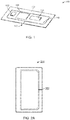
FIG. 1 illustrates a microelectronics package in accordance with embodiments disclosed herein. -
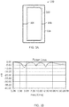
FIG. 2A illustrates a stiffening element in accordance with embodiments disclosed herein. -
FIG. 2B illustrates loss vs. frequency for the stiffening element inFIG. 2A . -
FIG. 2C illustrates peak gain vs. frequency for the stiffening element inFIG. 2A . -
FIG. 3A illustrates a stiffening element in accordance with embodiments disclosed herein. -
FIG. 3B illustrates loss vs. frequency for the stiffening element inFIG. 3A . -
FIG. 3C illustrates peak gain vs. frequency for the stiffening element inFIG. 3A . -
FIG. 4A illustrates a stiffening element in accordance with embodiments disclosed herein. -
FIG. 4B illustrates loss vs. frequency for the stiffening element inFIG. 4A . -
FIG. 4C illustrates peak gain vs. frequency for the stiffening element inFIG. 4A . -
FIGS. 5A and 5B illustrate microelectronics packages in accordance with embodiments disclosed herein. -
FIGS. 6A and 6B illustrate a microelectronics package in accordance with embodiments disclosed herein. -
FIG. 7 illustrates an example method for manufacturing a microelectronics package in accordance with embodiments disclosed herein. -
FIG. 8 illustrates an example process flow for manufacturing a microelectronics package in accordance with embodiments disclosed herein. -
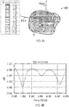
FIG. 9A illustrates a radiation pattern for a stiffening element in accordance with embodiments disclosed herein. -
FIG. 9B illustrates a return loss profile for a stiffening element in accordance with embodiments disclosed herein. -
FIG. 10A illustrates single magnetic loop antenna in accordance with embodiments disclosed herein. -
FIG. 10B illustrates a radiation pattern for the single magnetic loop antenna ofFIG. 10A in accordance with embodiments disclosed herein. -
FIG. 10C illustrates a return loss profile for the single magnetic loop antenna ofFIG. 10A in accordance with embodiments disclosed herein. -
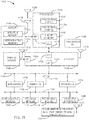
FIG. 11 illustrates an example schematic of a computing device in accordance with embodiments disclosed herein. - As disclosed herein, picture frame stiffening elements, or stiffeners, may be used in microelectronics packages. The stiffening element may be manufactured out of metal. The stiffening elements may cost between 15-20 cents/stiffener. The stiffeners may be used to stiffen the packages to help prevent structural warpage during use and surface mount technology (SMT) reflow.
- As disclosed herein, an on-package integrated stiffener antenna (oPiS antenna), may be used to augment the picture frame stiffener with antenna attributes as an integrated wireless antenna. For example, the stiffener may be fashioned into a single, arrays, loop, patch, hybrid, etc. on-package antenna. The oPiS antenna may be used as a solution for wireless applications such as, but not limited to, 5G, Intel WiGig, Intel WiDi, wireless charging etc.
- Turning now to the figures,
FIG. 1 illustrates amicroelectronics package 100 in accordance with embodiments disclosed herein. Themicroelectronics package 100 may include a radio frequency transmitter and/or receiver, (collectively referred to as transceiver 102), a platform controller hub (PCH) 104, and a central processing unit (CPU) 106. Other elements such as memory dies, additional processing dies, etc. may also be included in themicroelectronics package 100. Thetransceiver 102, thePCH 104, theCPU 106, and other components of thepackage 100 may be enclosed or otherwise shielded from astiffening element 108 by an electromagnetic interference (EMI)shield 110. TheEMI shield 110 may conform to the various components of thepackage 100. - The
stiffening element 108 may act as an antenna for thetransceiver 102. For example, as disclosed herein, thestiffening element 108 may be configured to act as an antenna and a traditional antenna may be excluded from thepackage 100. As used herein, a traditional antenna includes a separate element that one skilled in the art would understand to be an antenna normally included with a package to allow for wireless communications. - As disclose herein, the
stiffening element 108 may be manufactured from a conductive material such as a metal. Thestiffening element 108 may be configured, or tuned, to have a given resonant frequency and gain. For example, thestiffening element 108 may be trimmed and shaped to have an electrical length that yields a resonant frequency of about 1,000 MHz and a peak realized gain of about 10 dB. - The
stiffening element 108, may include acutout 112 that may serve as an antenna feed. For example, thecutout 112 may be part of a radiating slot used to form a magnetic loop antenna as shown inFIG. 2A , an electrical dipole design as shown inFIG. 3A , and a magnetic loop design as shown inFIG. 4A . - As disclosed herein, the
stiffening element 108 may be optimized, or tuned, to achieve a desired resonant frequency, loss, and gain. For example,FIGS. 2B ,3B , and4B show the return loss for the antenna designs shown inFIGS. 2A ,3A , and4A , respectively. In addition to being tuned for a desired resonant frequency, loss, and gain, thestiffening element 108 may also be manufactured to include antenna components. - For example, as shown in
FIGS. 2A , using the full perimeter length of thestiffener element 200 shown inFIG. 2A , the resonant frequency of thestiffener element 200 may be tuned to as low as 1.00 GHz and peak realized gain of 1.00GHz as illustrated inFIGS. 2B and 2C , respectively. As shown inFIG. 2A , thestiffening element 200 may include asingle feeding point 202. - The
stiffener element 300 shown inFIG. 3A may include afirst unit 302 and asecond unit 304 with feedingpoints stiffener element 300 shown inFIG. 3A the resonant frequency of thestiffener element 300 can be tuned to higher frequencies. In the example shown inFIG. 3A , the resonant frequency and noticeable peak realized gain starts at 4.20 GHz as shown inFIGS. 3B and3C . WhileFIG. 3A shows astiffening element 300 with theunits units first unit 302 may have a quarter perimeter length and thesecond unit 304 may have a three quarter perimeter length. - To further optimize the antenna radiation with better input impedance matching, the
stiffening element 400 shown inFIG. 4A may have a magnetic loop antenna design. The feeding points 402 and 404 of thestiffening element 400 are located on theouter rings first section 410 and asecond section 412. The configuration shown inFIG. 4A may widen the bandwidth of the resonant frequency and the peak realized gain as shown inFIGS. 4B and 4C . -
FIGS. 5A and 5B illustrate cross-sectional views ofmicroelectronics packages substrate 502. Thesubstrate 502 may be attached to a printed circuit board (PCB) (not shown) via one or more solder joints 504. Thesubstrate 502 also may include one or more vias that contain one or more feedlines 506. As disclosed herein, thefeedlines 506 may be used to electrically couple astiffening element 508 to asilicon component 510. Thesilicon component 510 may be a component of thetransceiver 102 or electrically coupled to thetransceiver 102. - As disclosed herein, the
stiffening element 508 may include apositive stiffening element 508+ and a negative stiffening element 508-. Thepositive stiffening element 508+ and the negative stiffening element 508- may be tuned as disclosed herein. Aconductive adhesive 512 may be used to secure thestiffening element 508 to thefeedlines 506. Theconductive adhesive 512 may rest on a solder resistlayer 514 and pass to thefeedlines 506 via one or more solder resistopenings 516. Thesilicon component 510 may be coupled to thefeedlines 506 via one or more solder bumps 518. Anunderfill 520 may be used to further secure thesilicon component 510 to the solder resistlayer 514. - As shown in
FIG. 5A , thestiffening element 508 may be tuned and trimmed such thatsidewalls sidewalls microelectronics package 500. As shown inFIG. 5B , thestiffening element 508 may be tuned and trimmed such thatsidewalls sidewalls microelectronics package 550. - The
stiffening element 508 extending past thesidewalls stiffening element 508. For example, the larger metal area may allow thestiffening element 508 to act as an antenna which is designed to operate at lower frequency/requires longer wavelength/requires longer electrical length to resonate. In addition, stiffeningelement 508 may be built using just the extension (i.e. portions extendingpast sidewalls 526 and 528) to resonate at higher frequency within the same stiffener length. This is due to the fact that the propagation medium for the extension (underneath the extension) is air instead of package substrate where air exhibits higher propagation velocity (i.e., shorter wavelength and requires shorter electrical length to resonate) than the package substrate. Furthermore, the medium underneath the extension can be filled with other dielectric material as another variable to configure thestiffening element 508's antenna electrical properties. -
FIGS. 6A and 6B illustrates a cross-sectional view ofmicroelectronics packages 600 in accordance with embodiments disclosed herein. Themicroelectronics package 600 may include asubstrate 602. Thesubstrate 602 may be attached to a printed circuit board (PCB) (not shown) via one or more solder joints 604. Thesubstrate 602 also may include one or more vias that contain one or more feedlines 606. As disclosed herein, thefeedlines 606 may be used to electrically couple astiffening element 608 to asilicon component 610. Thesilicon component 610 may be a component of thetransceiver 102 or electrically coupled to thetransceiver 102. - As disclosed herein, the
stiffening element 608 may include apositive stiffening element 608+ and a negative stiffening element 608-. Thepositive stiffening element 608+ and the negative stiffening element 608- may be tuned as disclosed herein. Aconductive adhesive 612 may be used to secure thestiffening element 608 to thefeedlines 606. Theconductive adhesive 612 may rest on a solder resistlayer 614 and pass to thefeedlines 606 via one or more solder resistopenings 616. Thesilicon component 610 may be coupled to thefeedlines 606 via one or more solder bumps 618. Anunderfill 620 may be used to further secure thesilicon component 610 to the solder resistlayer 614. - The
silicon component 610 may be surrounded on one or more sides by anEMI shield 630. TheEMI shield 630 may shield thesilicon component 610 from electromagnetic interference caused by the electromagnetic waves generated by or received by thestiffening element 608. In addition, theEMI shield 630 may shield thestiffening element 608 from electromagnetic interference from electromagnetic fields generated by thesilicon component 610. - To assist with further shielding of the
silicon component 610 and thestiffening element 608 from EMI, ametal layer 632 may be formed in between thestiffening component 610 and thesubstrate 602. Thestiffening element 610 may be secured to themetal layer 630 via anon-conductive adhesive 634. Themetal layer 632 may be secured to the solder resistlayer 614 via aconductive adhesive 636. Theconductive adhesive 636 may pass through a one ormore vias 638 and connect themetal layer 632 to aground layer 640. Thus, themetal layer 632 may be grounded. Themetal layer 632 may isolate thestiffening element 610 from surface routing interference for EMC alleviation. -
EMI shield 630 may be used to prevent electromagnetic interference from the silicon dies coupled onto the stiffening element causing unintentional radiation. TheEMI shield 630 may be grounded and may be directly grounded theground layer 640 or any other ground reference. - As shown in
FIG. 6 , thestiffening element 608 may be tuned and trimmed such thatsidewalls sidewalls microelectronics package 600. Just as is shown inFIG. 5B , thestiffening element 608 may be tuned and trimmed such thatsidewalls sidewalls microelectronics package 600. - As disclosed herein, the stiffening elements, such as stiffening
elements microelectronics packages -
FIG. 7 illustrates anexample method 700 for manufacturing a microelectronics package. Themethod 700 may begin atstage 702 where one or more dies may be attached to a substrate. The dies may be attached to one or more routing layers as is known in the art. - From
stage 702, themethod 700 may proceed to stage 704 where a metal layer may be formed. As disclosed herein, the metal layer may be formed such that a package stiffening element will be located proximate the metal layer and thus, act as a shield against magnetic interference. Also as disclosed herein, forming the metal layer can include electrically coupling the metal layer to a ground plane. - From
stage 704, themethod 700 may proceed to stage 706 where the package stiffening element may be formed. As disclosed herein forming the package stiffening element may include forming a cutout of a metal frame. Forming the package stiffening element may further include forming any number of antenna types. For example, the package stiffening element may be formed into a single antenna, an array loop antenna, a patch antenna, a magnetic loop antenna, or a hybrid antenna. - From
stage 706, themethod 700 may proceed to stage 708 where the package stiffening element may be tuned. For example, as disclosed herein, the package stiffening element may be trimmed, or tuned, to have a resonant frequency of about 1,000 MHz. The package stiffening element also may be tuned to have a peak realized gain of about 10 dB. Moreover, the package stiffening element may be tuned to have a circumference that is less than about 10% of a wavelength of a received electromagnetic waive. - From
stage 708, themethod 700 may proceed to stage 710 where an EMI shield may be attached. As disclosed herein, the EMI shield may cover dies, transmitters, receivers, transceivers, etc. In addition, the EMI shield may be electrically coupled to the metal layer or the ground plane. The EMI shield may be formed via sputtering techniques. Also, the EMI shield may be preformed and then bound to the dies or substrate. - From
stage 710, themethod 700 may proceed to stage 712 where the package stiffening element may be attached. For example, the package stiffening element may be attached to a microelectronics package and coupled to one or more of the dies such that the package stiffening element is configured to act as an antenna for a transmitter, receiver, or transceiver. As disclosed herein, the package stiffening element may be used as an antenna such that a traditional antenna need not be attached to the microelectronics package. - While the stages of the
method 700 have been described in one order in this disclosure, the stages of themethod 700 need not be performed in the order described herein. For example, the package stiffening element may be attached to the microelectronics package before the EMI shield is attached. In addition, the package stiffening element may be attached before the dies are attached to the substrate. -
FIG. 8 shows aprocess flow 800 for manufacturing a microelectronics package. Theprocess flow 800 may begin with apost assembly package 802 and apackage stiffening element 804 may be received from manufacturers. Thepost assembly package 802 may be manufactured using known techniques and include routing layers, ground layers, metal layers, a substrate, dies, etc. as disclosed herein. Thepackage stiffening element 804 may be received from a stiffening element manufacturer. The stiffening element manufacturer may manufacture thepackage stiffening element 804 as disclosed herein so that the package stiffening element is tuned to act an antenna. - Once the
post assembly package 802 and thepackage stiffening element 804 are received, thepackage stiffening element 804 may be attached to thepost assembly package 802. For example, as disclosed herein, a conductive adhesive or a non-conductive adhesive may be used to attach portions of thepackage stiffening element 804 to thepost assembly package 802. - Once the
package stiffening element 804 is attached to thepost assembly package 802, theEMI shield 806 can be attached to thepost assembly package 802. TheEMI shield 806 may also be attached by the manufacturer of thepost assembly package 802. -
FIGS. 9A and 9B illustrate aradiation pattern 902 and a plot 904 showing return losses for a single package with a single stiffener element (i.e., the magnetic loop antenna formed by stiffening element 200) that has not been placed on a printed circuit board. In contrast, as shown inFIG. 10A , when asingle package 1002 with a single stiffener element 1004 (i.e., the magnetic loop antenna formed by stiffening element 200) is soldered onto a large printedcircuit board 1006, itsradiation pattern 1008 is maintained in an upward facing direction and resonant frequency are still consistent despite with the presents of the large ground plane of the printed circuit board, as shown in theFIGS. 10B and10C . -
FIG. 11 illustrates a system level diagram, according to one embodiment of the invention. For instance,FIG. 11 depicts an example of an electronic device (e.g., system) including the microelectronics package disclosed herein.FIG. 11 is included to show an example of a higher level device application for the present invention. In one embodiment,system 1100 includes, but is not limited to, a desktop computer, a laptop computer, a netbook, a tablet, a notebook computer, a personal digital assistant (PDA), a server, a workstation, a cellular telephone, a mobile computing device, a smart phone, an Internet appliance or any other type of computing device. In some embodiments,system 1100 is a system on a chip (SOC) system. - In one embodiment,
processor 1110 has one ormore processing cores processor 110 where N is a positive integer. In one embodiment,system 1100 includes multiple processors including 1110 and 105, where processor 105 has logic similar or identical to the logic ofprocessor 1110. In some embodiments, processingcore 1112 includes, but is not limited to, pre-fetch logic to fetch instructions, decode logic to decode the instructions, execution logic to execute instructions and the like. In some embodiments,processor 1110 has acache memory 1116 to cache instructions and/or data forsystem 1100.Cache memory 1116 may be organized into a hierarchal structure including one or more levels of cache memory. - In some embodiments,
processor 1110 includes amemory controller 1114, which is operable to perform functions that enable theprocessor 1110 to access and communicate withmemory 1130 that includes avolatile memory 1132 and/or anon-volatile memory 1134. In some embodiments,processor 1110 is coupled withmemory 1130 andchipset 1120.Processor 1110 may also be coupled to awireless antenna 1178 to communicate with any device configured to transmit and/or receive wireless signals. In one embodiment, thewireless antenna interface 1178 operates in accordance with, but is not limited to, the IEEE 802.11 standard and its related family, Home Plug AV (HPAV), Ultra Wide Band (UWB), Bluetooth, WiMax, or any form of wireless communication protocol. In addition, as disclosed herein, thewireless antenna interface 1178 may be the stiffening elements disclosed herein. - In some embodiments,
volatile memory 1132 includes, but is not limited to, Synchronous Dynamic Random Access Memory (SDRAM), Dynamic Random Access Memory (DRAM), RAMBUS Dynamic Random Access Memory (RDRAM), and/or any other type of random access memory device.Non-volatile memory 1134 includes, but is not limited to, flash memory, phase change memory (PCM), read-only memory (ROM), electrically erasable programmable read-only memory (EEPROM), or any other type of non-volatile memory device. -
Memory 1130 stores information and instructions to be executed byprocessor 1110. In one embodiment,memory 1130 may also store temporary variables or other intermediate information whileprocessor 1110 is executing instructions. In the illustrated embodiment,chipset 1120 connects withprocessor 1110 via Point-to-Point (PtP or P-P) interfaces 1117 and 1122.Chipset 1120 enablesprocessor 1110 to connect to other elements insystem 1100. In some embodiments of the invention, interfaces 1117 and 1122 operate in accordance with a PtP communication protocol such as the Intel® QuickPath Interconnect (QPI) or the like. In other embodiments, a different interconnect may be used. - In some embodiments,
chipset 1120 is operable to communicate withprocessor 1110, 1105N,display device 1140, andother devices Chipset 1120 may also be coupled to awireless antenna 1178 to communicate with any device configured to transmit and/or receive wireless signals. In addition, as disclosed herein, thewireless antenna interface 1178 may be the stiffening elements disclosed herein. -
Chipset 1120 connects to displaydevice 1140 viainterface 1126.Display 1140 may be, for example, a liquid crystal display (LCD), a plasma display, cathode ray tube (CRT) display, or any other form of visual display device. In some embodiments of the invention,processor 1110 andchipset 1120 are merged into a single SOC. In addition,chipset 1120 connects to one ormore buses various elements Buses bus bridge 1172. In one embodiment,chipset 1120 couples with anon-volatile memory 1160, a mass storage device(s) 1162, a keyboard/mouse 1164, and anetwork interface 1166 viainterface 1124 and/or 1104,smart TV 1176,consumer electronics 1177, etc. - In one embodiment,
mass storage device 1162 includes, but is not limited to, a solid state drive, a hard disk drive, a universal serial bus flash memory drive, or any other form of computer data storage medium. In one embodiment,network interface 1166 is implemented by any type of well known network interface standard including, but not limited to, an Ethernet interface, a universal serial bus (USB) interface, a Peripheral Component Interconnect (PCI) Express interface, a wireless interface and/or any other suitable type of interface. In one embodiment, the wireless interface operates in accordance with, but is not limited to, the IEEE 802.11 standard and its related family, Home Plug AV (HPAV), Ultra Wide Band (UWB), Bluetooth, WiMax, or any form of wireless communication protocol. In addition, as disclosed herein, the wireless interface may be the stiffening elements disclosed herein. - While the modules shown in
FIG. 11 are depicted as separate blocks within thesystem 1100, the functions performed by some of these blocks may be integrated within a single semiconductor circuit or may be implemented using two or more separate integrated circuits. For example, althoughcache memory 1116 is depicted as a separate block withinprocessor 1110, cache memory 1116 (or selected aspects of 1116) can be incorporated intoprocessor core 1112. -
- Example 1 is a microelectronics package comprising: a transmitter; a receiver; and a package stiffening element in electrical communication with the transmitter and the receiver, the package stiffening element configured to act as an antenna for both the transmitter and the receiver.
- In Example 2, the subject matter of Example 1 optionally includes wherein a traditional antenna is not included in the microelectronics package.
- In Example 3, the subject matter of any one or more of Examples 1-2 optionally include wherein package stiffening element supports multiple communication types.
- In Example 4, the subject matter of any one or more of Examples 1-3 optionally include wherein the transmitter and the receiver are components of a transceiver.
- In Example 5, the subject matter of any one or more of Examples 1-4 optionally include wherein the package stiffening element forms a magnetic loop antenna.
- In Example 6, the subject matter of Example 5 optionally includes % of a wavelength of a received electromagnetic wave.
- In Example 7, the subject matter of any one or more of Examples 1-6 optionally include wherein the package stiffening element forms a dipole antenna, a single antenna, an array loop antenna, a patch antenna, or a hybrid antenna.
- In Example 8, the subject matter of any one or more of Examples 1-7 optionally include wherein the package stiffening element is positioned along a perimeter of the microelectronics package.
- In Example 9, the subject matter of any one or more of Examples 1-8 optionally include wherein the package stiffening element at least partially encircles the transmitter, the receiver, and one or more dies forming the microelectronics package.
- In Example 10, the subject matter of any one or more of Examples 1-9 optionally include wherein the package stiffening element is bonded to the microelectronics package via a non-conductive adhesive.
- In Example 11, the subject matter of any one or more of Examples 1-10 optionally include an electromagnetic interference shield surrounding the transmitter and the receiver, the package stiffening element encircling a portion of the electromagnetic interference shield.
- In Example 12, the subject matter of any one or more of Examples 1-11 optionally include MHz.
- In Example 13, the subject matter of any one or more of Examples 1-12 optionally include dB.
- In Example 14, the subject matter of any one or more of Examples 1-13 optionally include wherein the package stiffening element includes a first portion and second portion, the first portion in electrical communication with the transmitter and the second portion in electrical communication with the receiver.
- In Example 15, the subject matter of any one or more of Examples 1-14 optionally include wherein the package stiffening element includes a plurality of portions, each of the plurality of portions supporting a different communication type.
- In Example 16, the subject matter of any one or more of Examples 1-15 optionally include wherein the package stiffening element extends beyond a ground plane of the microelectronics package.
- In Example 17, the subject matter of any one or more of Examples 1-16 optionally include wherein the package stiffening element forms a Wi-Fi antenna.
- In Example 18, the subject matter of any one or more of Examples 1-17 optionally include wherein the package stiffening element forms a Bluetooth antenna.
- In Example 19, the subject matter of any one or more of Examples 1-18 optionally include wherein the package stiffening element forms a near-field-communications antenna.
- In Example 20, the subject matter of any one or more of Examples 1-19 optionally include wherein package stiffening element forms a cellular antenna.
- Example 21 is a microelectronics package comprising: a ground plane; a plurality of dies electrically coupled to the ground plane; a transceiver; and a package stiffening element located proximate the ground plane and in electrical communication with the transceiver, the package stiffening element configured to act as an antenna for the transceiver.
- In Example 22, the subject matter of any one or more of Examples 1-21 optionally include wherein a traditional antenna is not included in the microelectronics package.
- In Example 23, the subject matter of any one or more of Examples 21-22 optionally include wherein package stiffening element supports multiple communication types.
- In Example 24, the subject matter of any one or more of Examples 21-23 optionally include wherein the package stiffening element forms a magnetic loop antenna.
- In Example 25, the subject matter of Example 24 optionally includes % of a wavelength of a received electromagnetic wave.
- In Example 26, the subject matter of any one or more of Examples 21-25 optionally include wherein the package stiffening element forms a dipole antenna, a single antenna, an array loop antenna, a patch antenna, or a hybrid antenna.
- In Example 27, the subject matter of any one or more of Examples 21-26 optionally include wherein the package stiffening element is positioned along a perimeter of the ground plane.
- In Example 28, the subject matter of any one or more of Examples 21-27 optionally include wherein the package stiffening element at least partially encircles the transceiver and the plurality of dies.
- In Example 29, the subject matter of any one or more of Examples 21-28 optionally include wherein the package stiffening element is bonded to the microelectronics package via a non-conductive adhesive.
- In Example 30, the subject matter of any one or more of Examples 21-29 optionally include an electromagnetic interference shield surrounding the transceiver and the plurality of dies, the package stiffening element encircling at least a portion of the electromagnetic interference shield.
- In Example 31, the subject matter of any one or more of Examples 21-30 optionally include MHz.
- In Example 32, the subject matter of any one or more of Examples 21-31 optionally include dB.
- In Example 33, the subject matter of any one or more of Examples 21-32 optionally include wherein the package stiffening element includes a first portion and second portion, the first portion in electrical communication with the transmitter and the second portion in electrical communication with the receiver.
- In Example 34, the subject matter of any one or more of Examples 21-33 optionally include wherein the package stiffening element includes a plurality of portions, each of the plurality of portions supporting a different communication type.
- In Example 35, the subject matter of any one or more of Examples 21-34 optionally include wherein the package stiffening element extends beyond a perimeter of the ground plane.
- In Example 36, the subject matter of any one or more of Examples 21-35 optionally include wherein the package stiffening element forms a Wi-Fi antenna.
- In Example 37, the subject matter of any one or more of Examples 21-36 optionally include wherein the package stiffening element forms a Bluetooth antenna.
- In Example 38, the subject matter of any one or more of Examples 21-37 optionally include wherein the package stiffening element forms a near-field-communications antenna.
- In Example 39, the subject matter of any one or more of Examples 21-38 optionally include wherein package stiffening element forms a cellular antenna.
- Example 40 is a method of manufacturing a microelectronics package, the method comprising: attaching a plurality of dies to a substrate; tuning a package stiffening element to have a predetermined resonate frequency; attaching the package stiffening element to the substrate; and electrically coupling the package stiffening element to at least one of the plurality of dies such that the package stiffening element is an antenna for both a transmitter and a receiver.
- In Example 41, the subject matter of Example 40 optionally includes forming a ground plane proximate the plurality of dies, wherein the package stiffening element is proximate a perimeter of the ground plane.
- In Example 42, the subject matter of any one or more of Examples 40-41 optionally include forming a ground plane proximate the plurality of dies, wherein the package stiffening element extends beyond a perimeter of the ground plane.
- In Example 43, the subject matter of any one or more of Examples 40-42 optionally include wherein electrically coupling the transmitter to the at least one of the plurality of dies includes locating a feeding point proximate the transmitter.
- In Example 44, the subject matter of any one or more of Examples 40-43 optionally include MHz.
- In Example 45, the subject matter of any one or more of Examples 40-44 optionally include dB.
- In Example 46, the subject matter of any one or more of Examples 40-45 optionally include forming an electromagnetic interference shield that at least partially encircles the plurality of dies.
- In Example 47, the subject matter of Example 46 optionally includes wherein attaching the package stiffening element includes attaching the package stiffening element such that the package stiffening element at least partially encircles the electromagnetic interference shield.
- In Example 48, the subject matter of any one or more of Examples 40-47 optionally include forming the package stiffening element to create a single antenna.
- In Example 49, the subject matter of any one or more of Examples 40-48 optionally include forming the package stiffening element to create an array loop antenna.
- In Example 50, the subject matter of any one or more of Examples 40-49 optionally include forming the package stiffening element to create a patch antenna.
- In Example 51, the subject matter of any one or more of Examples 40-50 optionally include forming the package stiffening element to create a hybrid antenna.
- In Example 52, the subject matter of any one or more of Examples 40-51 optionally include forming the package stiffening element to create a magnetic loop antenna.
- In Example 53, the subject matter of Example 52 optionally includes % of a wavelength of a received electromagnetic wave.
- Example 54 is a microelectronics package comprising: means for transmitting a first electromagnetic wave, the transmitting means attached to a substrate; means for receiving a second electromagnetic wave, the receiving means attached to the substrate; and stiffening means in electrical communication with both the transmitting means and the receiving means, the stiffening means forming an antenna for the transmitting means and the receiving means.
- In Example 55, the subject matter of Example 54 optionally includes wherein the microelectronics package does not include a traditional antenna.
- In Example 56, the subject matter of any one or more of Examples 54-55 optionally include means for shielding the stiffening means from electromagnetic radiation emitted from a die located proximate the stiffening means.
- In Example 57, the subject matter of any one or more of Examples 54-56 optionally include grounding means located proximate the stiffening means.
- In Example 58, the subject matter of any one or more of Examples 54-57 optionally include ground means, wherein the package stiffening element extends beyond a perimeter of the grounding means.
- In Example 59, the subject matter of any one or more of Examples 54-58 optionally include wherein stiffening means supports multiple communication types.
- In Example 60, the subject matter of any one or more of Examples 54-59 optionally include wherein the stiffening means forms a magnetic loop antenna, a dipole antenna, a single antenna, an array loop antenna, a patch antenna, or a hybrid antenna.
- In Example 61, the subject matter of any one or more of Examples 54-60 optionally include wherein the stiffening means is positioned along a perimeter of the microelectronics package.
- In Example 62, the subject matter of any one or more of Examples 54-61 optionally include wherein the stiffening means at least partially encircles the transmitting means, the receiving means, and one or more dies forming the microelectronics package.
- In Example 63, the subject matter of any one or more of Examples 54-62 optionally include wherein the stiffening means is bonded to the microelectronics package via a non-conductive adhesive.
- In Example 64, the subject matter of any one or more of Examples 54-63 optionally include MHz.
- In Example 65, the subject matter of any one or more of Examples 54-64 optionally include dB.
- In Example 66, the subject matter of any one or more of Examples 54-65 optionally include wherein the stiffening means includes a first portion and second portion, the first portion in electrical communication with the transmitting means and the second portion in electrical communication with the receiving means.
- In Example 67, the subject matter of any one or more of Examples 54-66 optionally include wherein the stiffening means includes a plurality of portions, each of the plurality of portions supporting a different communication type.
- The above detailed description includes references to the accompanying drawings, which form a part of the detailed description. The drawings show, by way of illustration, specific embodiments that may be practiced. These embodiments are also referred to herein as "examples." Such examples may include elements in addition to those shown or described. However, also contemplated are examples that include the elements shown or described. Moreover, also contemplate are examples using any combination or permutation of those elements shown or described (or one or more aspects thereof), either with respect to a particular example (or one or more aspects thereof), or with respect to other examples (or one or more aspects thereof) shown or described herein.
- Publications, patents, and patent documents referred to in this document are incorporated by reference herein in their entirety, as though individually incorporated by reference. In the event of inconsistent usages between this document and those documents so incorporated by reference, the usage in the incorporated reference(s) are supplementary to that of this document; for irreconcilable inconsistencies, the usage in this document controls.
- In this document, the terms "a" or "an" are used, as is common in patent documents, to include one or more than one, independent of any other instances or usages of "at least one" or "one or more." In this document, the term "or" is used to refer to a nonexclusive or, such that "A or B" includes "A but not B," "B but not A," and "A and B," unless otherwise indicated. In the appended claims, the terms "including" and "in which" are used as the plain-English equivalents of the respective terms "comprising" and "wherein." Also, in the following claims, the terms "including" and "comprising" are open-ended, that is, a system, device, article, or process that includes elements in addition to those listed after such a term in a claim are still deemed to fall within the scope of that claim. Moreover, in the following claims, the terms "first," "second," and "third," etc. are used merely as labels, and are not intended to suggest a numerical order for their objects.
- The above description is intended to be illustrative, and not restrictive. For example, the above-described examples (or one or more aspects thereof) may be used in combination with others. Other embodiments may be used, such as by one of ordinary skill in the art upon reviewing the above description. The Abstract is to allow the reader to quickly ascertain the nature of the technical disclosure and is submitted with the understanding that it will not be used to interpret or limit the scope or meaning of the claims. Also, in the above Detailed Description, various features may be grouped together to streamline the disclosure. However, the claims may not set forth features disclosed herein because embodiments may include a subset of said features. Further, embodiments may include fewer features than those disclosed in a particular example. Thus, the following claims are hereby incorporated into the Detailed Description, with a claim standing on its own as a separate embodiment. The scope of the embodiments disclosed herein is to be determined with reference to the appended claims, along with the full scope of equivalents to which such claims are entitled.
Claims (15)
- A microelectronics package comprising:a transmitter;a receiver; anda package stiffening element in electrical communication with the transmitter and the receiver, the package stiffening element configured to act as an antenna for both the transmitter and the receiver.
- The microelectronics package of claim 1, wherein a traditional antenna is not included in the microelectronics package.
- The microelectronics package of any one of or any combination of claims 1 and 2, wherein package stiffening element supports multiple communication types.
- The microelectronics package of any one of or any combination of claims 1-3, wherein the package stiffening element forms a dipole antenna, a single antenna, an array loop antenna, a patch antenna, or a hybrid antenna.
- The microelectronics package of any one of or any combination of claims 1-4, wherein the package stiffening element is positioned along a perimeter of the microelectronics package.
- The microelectronics package of any one of or any combination of claims 1-5, wherein the package stiffening element at least partially encircles the transmitter, the receiver, and one or more dies forming the microelectronics package.
- The microelectronics package of any one of or any combination of claims 1-6, wherein the package stiffening element is bonded to the microelectronics package via a non-conductive adhesive.
- The microelectronics package of any one of or any combination of claims 1-7, further comprising an electromagnetic interference shield surrounding the transmitter and the receiver, the package stiffening element encircling a portion of the electromagnetic interference shield.
- The microelectronics package of any one of or any combination of claims 1-8, wherein the package stiffening element has a resonant frequency of about 1,000 MHz.
- The microelectronics package of any one of or any combination of claims 1-9, wherein the package stiffening element has a peak realized gain of about 10 dB.
- A method of manufacturing a microelectronics package, the method comprising:attaching a plurality of dies to a substrate;tuning a package stiffening element to have a predetermined resonate frequency;attaching the package stiffening element to the substrate; andelectrically coupling the package stiffening element to at least one of the plurality of dies such that the package stiffening element is an antenna for both a transmitter and a receiver.
- The method of claim 11, further comprising forming a ground plane proximate the plurality of dies, wherein the package stiffening element is proximate a perimeter of the ground plane.
- The method of claim 11, further comprising forming a ground plane proximate the plurality of dies, wherein the package stiffening element extends beyond a perimeter of the ground plane.
- The method of any one of or any combination of claims 11-13, wherein tuning the package stiffening element to have the predetermined resonant frequency comprises tuning the package stiffening element to have a resonant frequency of about 1,000 MHz.
- The method of any one of or any combination of claims 11-14, wherein tuning the package stiffening element to have the predetermined resonant frequency comprises tuning the package stiffening element to have a peak realized gain of about 10 dB.
Applications Claiming Priority (1)
| Application Number | Priority Date | Filing Date | Title |
|---|---|---|---|
| US15/869,992 US20190221529A1 (en) | 2018-01-12 | 2018-01-12 | On-package integrated stiffener antenna |
Publications (2)
| Publication Number | Publication Date |
|---|---|
| EP3512034A1 true EP3512034A1 (en) | 2019-07-17 |
| EP3512034B1 EP3512034B1 (en) | 2021-09-08 |
Family
ID=64664947
Family Applications (1)
| Application Number | Title | Priority Date | Filing Date |
|---|---|---|---|
| EP18211799.4A Active EP3512034B1 (en) | 2018-01-12 | 2018-12-11 | On-package integrated stiffener antenna |
Country Status (3)
| Country | Link |
|---|---|
| US (1) | US20190221529A1 (en) |
| EP (1) | EP3512034B1 (en) |
| CN (1) | CN110034083A (en) |
Cited By (1)
| Publication number | Priority date | Publication date | Assignee | Title |
|---|---|---|---|---|
| CN111276787A (en) * | 2019-12-31 | 2020-06-12 | 中国电子科技集团公司第五十五研究所 | 3D Integrated Millimeter-Wave AiP Phased Array Element |
Families Citing this family (4)
| Publication number | Priority date | Publication date | Assignee | Title |
|---|---|---|---|---|
| CN111106418B (en) * | 2018-10-29 | 2022-10-14 | 康普技术有限责任公司 | LF and DC signal isolation devices and antennas |
| US10943874B1 (en) * | 2019-08-29 | 2021-03-09 | Juniper Networks, Inc | Apparatus, system, and method for mitigating warpage of integrated circuits during reflow processes |
| US11101541B2 (en) * | 2019-10-03 | 2021-08-24 | Advanced Semiconductor Engineering, Inc. | Semiconductor assembly and method for manufacturing the same |
| US10916843B1 (en) * | 2019-10-29 | 2021-02-09 | Terrance O'Brien Woodbridge | Method and system to reduce the impact of electromagnetic pulses on cellular tower sites |
Citations (3)
| Publication number | Priority date | Publication date | Assignee | Title |
|---|---|---|---|---|
| US20070231962A1 (en) * | 2006-03-29 | 2007-10-04 | Shinko Electric Industries Co., Ltd. | Manufacturing method of wiring substrate and manufacturing method of semiconductor device |
| US20100026601A1 (en) * | 2008-08-04 | 2010-02-04 | Chung-Long Chang | Antennas Integrated in Semiconductor Chips |
| US20160268213A1 (en) * | 2015-03-09 | 2016-09-15 | Intel Corporation | On Package Floating Metal/Stiffener Grounding to Mitigate RFI and SI Risks |
Family Cites Families (4)
| Publication number | Priority date | Publication date | Assignee | Title |
|---|---|---|---|---|
| US7369090B1 (en) * | 2001-05-17 | 2008-05-06 | Cypress Semiconductor Corp. | Ball Grid Array package having integrated antenna pad |
| EP1970951A3 (en) * | 2007-03-13 | 2009-05-06 | Semiconductor Energy Laboratory Co., Ltd. | Semiconductor device and manufacturing method thereof |
| US9160068B2 (en) * | 2013-05-09 | 2015-10-13 | Google Technology Holdings LLC | Systems and methods for antenna arrangements in an electronic device |
| US10992055B2 (en) * | 2016-04-28 | 2021-04-27 | At&S Austria Technologie & Systemtechnik Aktiengesellschaft | Component carrier with integrated antenna arrangement, electronic apparatus, radio communication method |
-
2018
- 2018-01-12 US US15/869,992 patent/US20190221529A1/en not_active Abandoned
- 2018-12-11 EP EP18211799.4A patent/EP3512034B1/en active Active
- 2018-12-12 CN CN201811516396.XA patent/CN110034083A/en active Pending
Patent Citations (3)
| Publication number | Priority date | Publication date | Assignee | Title |
|---|---|---|---|---|
| US20070231962A1 (en) * | 2006-03-29 | 2007-10-04 | Shinko Electric Industries Co., Ltd. | Manufacturing method of wiring substrate and manufacturing method of semiconductor device |
| US20100026601A1 (en) * | 2008-08-04 | 2010-02-04 | Chung-Long Chang | Antennas Integrated in Semiconductor Chips |
| US20160268213A1 (en) * | 2015-03-09 | 2016-09-15 | Intel Corporation | On Package Floating Metal/Stiffener Grounding to Mitigate RFI and SI Risks |
Cited By (1)
| Publication number | Priority date | Publication date | Assignee | Title |
|---|---|---|---|---|
| CN111276787A (en) * | 2019-12-31 | 2020-06-12 | 中国电子科技集团公司第五十五研究所 | 3D Integrated Millimeter-Wave AiP Phased Array Element |
Also Published As
| Publication number | Publication date |
|---|---|
| CN110034083A (en) | 2019-07-19 |
| EP3512034B1 (en) | 2021-09-08 |
| US20190221529A1 (en) | 2019-07-18 |
Similar Documents
| Publication | Publication Date | Title |
|---|---|---|
| EP3512034B1 (en) | On-package integrated stiffener antenna | |
| US11784417B2 (en) | Antenna and communications apparatus | |
| CN101438555B (en) | Multiband antenna array using electromagnetic bandgap structures | |
| US11764489B2 (en) | Sub-module L-shaped millimeter wave antenna-in-package | |
| US9368873B2 (en) | Triple-band antenna and method of manufacture | |
| US20180226727A1 (en) | Module, wireless communication apparatus, and radar apparatus | |
| US9502776B2 (en) | Antenna surrounded by metal housing | |
| US9300055B2 (en) | Mobile device with two antennas and antenna switch modules | |
| US20220085493A1 (en) | Housing assembly, antenna device, and electronic device | |
| US20140203974A1 (en) | Electronic device and antenna unit thereof | |
| CN111864411B (en) | Antenna module, terminal, control method, control device and storage medium | |
| CN110048230B (en) | Compact Antenna and Mobile Terminal | |
| US9583842B2 (en) | System and method for attaching solder balls and posts in antenna areas | |
| JP2017532886A (en) | Multiband antenna and communication terminal | |
| CN102820523B (en) | multi-frequency antenna | |
| JP2016072951A (en) | Wireless communication device | |
| CN108736132A (en) | Antenna module and electronic device | |
| CN104753554B (en) | Radio frequency device and wireless communication device | |
| US8384608B2 (en) | Slot antenna | |
| JP2003198248A (en) | Antenna integrated package | |
| JP7064511B2 (en) | Antenna module and terminal | |
| CN121844449A (en) | Antenna assembly | |
| CN104852140B (en) | Resonance circuit capable of suppressing interference between high-frequency connector and antenna | |
| CN115911859B (en) | Antenna structure and electronic equipment | |
| CN104779966A (en) | Wireless communication device |
Legal Events
| Date | Code | Title | Description |
|---|---|---|---|
| PUAI | Public reference made under article 153(3) epc to a published international application that has entered the european phase |
Free format text: ORIGINAL CODE: 0009012 |
|
| STAA | Information on the status of an ep patent application or granted ep patent |
Free format text: STATUS: THE APPLICATION HAS BEEN PUBLISHED |
|
| AK | Designated contracting states |
Kind code of ref document: A1 Designated state(s): AL AT BE BG CH CY CZ DE DK EE ES FI FR GB GR HR HU IE IS IT LI LT LU LV MC MK MT NL NO PL PT RO RS SE SI SK SM TR |
|
| AX | Request for extension of the european patent |
Extension state: BA ME |
|
| STAA | Information on the status of an ep patent application or granted ep patent |
Free format text: STATUS: REQUEST FOR EXAMINATION WAS MADE |
|
| 17P | Request for examination filed |
Effective date: 20200117 |
|
| RBV | Designated contracting states (corrected) |
Designated state(s): AL AT BE BG CH CY CZ DE DK EE ES FI FR GB GR HR HU IE IS IT LI LT LU LV MC MK MT NL NO PL PT RO RS SE SI SK SM TR |
|
| GRAP | Despatch of communication of intention to grant a patent |
Free format text: ORIGINAL CODE: EPIDOSNIGR1 |
|
| STAA | Information on the status of an ep patent application or granted ep patent |
Free format text: STATUS: GRANT OF PATENT IS INTENDED |
|
| RIC1 | Information provided on ipc code assigned before grant |
Ipc: H01L 21/56 20060101ALN20210310BHEP Ipc: H04B 1/3888 20150101ALI20210310BHEP Ipc: H01L 23/66 20060101ALI20210310BHEP Ipc: H01L 23/00 20060101ALI20210310BHEP Ipc: H01L 23/552 20060101ALI20210310BHEP Ipc: H01Q 7/00 20060101ALI20210310BHEP Ipc: H01Q 1/44 20060101ALI20210310BHEP Ipc: H01Q 1/22 20060101AFI20210310BHEP |
|
| RIC1 | Information provided on ipc code assigned before grant |
Ipc: H01L 21/56 20060101ALN20210323BHEP Ipc: H04B 1/3888 20150101ALI20210323BHEP Ipc: H01L 23/66 20060101ALI20210323BHEP Ipc: H01L 23/00 20060101ALI20210323BHEP Ipc: H01L 23/552 20060101ALI20210323BHEP Ipc: H01Q 7/00 20060101ALI20210323BHEP Ipc: H01Q 1/44 20060101ALI20210323BHEP Ipc: H01Q 1/22 20060101AFI20210323BHEP |
|
| INTG | Intention to grant announced |
Effective date: 20210414 |
|
| GRAS | Grant fee paid |
Free format text: ORIGINAL CODE: EPIDOSNIGR3 |
|
| GRAA | (expected) grant |
Free format text: ORIGINAL CODE: 0009210 |
|
| STAA | Information on the status of an ep patent application or granted ep patent |
Free format text: STATUS: THE PATENT HAS BEEN GRANTED |
|
| AK | Designated contracting states |
Kind code of ref document: B1 Designated state(s): AL AT BE BG CH CY CZ DE DK EE ES FI FR GB GR HR HU IE IS IT LI LT LU LV MC MK MT NL NO PL PT RO RS SE SI SK SM TR |
|
| REG | Reference to a national code |
Ref country code: GB Ref legal event code: FG4D |
|
| REG | Reference to a national code |
Ref country code: AT Ref legal event code: REF Ref document number: 1429393 Country of ref document: AT Kind code of ref document: T Effective date: 20210915 Ref country code: CH Ref legal event code: EP |
|
| REG | Reference to a national code |
Ref country code: IE Ref legal event code: FG4D |
|
| REG | Reference to a national code |
Ref country code: DE Ref legal event code: R096 Ref document number: 602018023181 Country of ref document: DE |
|
| REG | Reference to a national code |
Ref country code: NL Ref legal event code: FP |
|
| REG | Reference to a national code |
Ref country code: LT Ref legal event code: MG9D |
|
| PG25 | Lapsed in a contracting state [announced via postgrant information from national office to epo] |
Ref country code: HR Free format text: LAPSE BECAUSE OF FAILURE TO SUBMIT A TRANSLATION OF THE DESCRIPTION OR TO PAY THE FEE WITHIN THE PRESCRIBED TIME-LIMIT Effective date: 20210908 Ref country code: FI Free format text: LAPSE BECAUSE OF FAILURE TO SUBMIT A TRANSLATION OF THE DESCRIPTION OR TO PAY THE FEE WITHIN THE PRESCRIBED TIME-LIMIT Effective date: 20210908 Ref country code: ES Free format text: LAPSE BECAUSE OF FAILURE TO SUBMIT A TRANSLATION OF THE DESCRIPTION OR TO PAY THE FEE WITHIN THE PRESCRIBED TIME-LIMIT Effective date: 20210908 Ref country code: RS Free format text: LAPSE BECAUSE OF FAILURE TO SUBMIT A TRANSLATION OF THE DESCRIPTION OR TO PAY THE FEE WITHIN THE PRESCRIBED TIME-LIMIT Effective date: 20210908 Ref country code: SE Free format text: LAPSE BECAUSE OF FAILURE TO SUBMIT A TRANSLATION OF THE DESCRIPTION OR TO PAY THE FEE WITHIN THE PRESCRIBED TIME-LIMIT Effective date: 20210908 Ref country code: BG Free format text: LAPSE BECAUSE OF FAILURE TO SUBMIT A TRANSLATION OF THE DESCRIPTION OR TO PAY THE FEE WITHIN THE PRESCRIBED TIME-LIMIT Effective date: 20211208 Ref country code: LT Free format text: LAPSE BECAUSE OF FAILURE TO SUBMIT A TRANSLATION OF THE DESCRIPTION OR TO PAY THE FEE WITHIN THE PRESCRIBED TIME-LIMIT Effective date: 20210908 Ref country code: NO Free format text: LAPSE BECAUSE OF FAILURE TO SUBMIT A TRANSLATION OF THE DESCRIPTION OR TO PAY THE FEE WITHIN THE PRESCRIBED TIME-LIMIT Effective date: 20211208 |
|
| REG | Reference to a national code |
Ref country code: AT Ref legal event code: MK05 Ref document number: 1429393 Country of ref document: AT Kind code of ref document: T Effective date: 20210908 |
|
| PG25 | Lapsed in a contracting state [announced via postgrant information from national office to epo] |
Ref country code: LV Free format text: LAPSE BECAUSE OF FAILURE TO SUBMIT A TRANSLATION OF THE DESCRIPTION OR TO PAY THE FEE WITHIN THE PRESCRIBED TIME-LIMIT Effective date: 20210908 Ref country code: GR Free format text: LAPSE BECAUSE OF FAILURE TO SUBMIT A TRANSLATION OF THE DESCRIPTION OR TO PAY THE FEE WITHIN THE PRESCRIBED TIME-LIMIT Effective date: 20211209 |
|
| PG25 | Lapsed in a contracting state [announced via postgrant information from national office to epo] |
Ref country code: AT Free format text: LAPSE BECAUSE OF FAILURE TO SUBMIT A TRANSLATION OF THE DESCRIPTION OR TO PAY THE FEE WITHIN THE PRESCRIBED TIME-LIMIT Effective date: 20210908 |
|
| PG25 | Lapsed in a contracting state [announced via postgrant information from national office to epo] |
Ref country code: IS Free format text: LAPSE BECAUSE OF FAILURE TO SUBMIT A TRANSLATION OF THE DESCRIPTION OR TO PAY THE FEE WITHIN THE PRESCRIBED TIME-LIMIT Effective date: 20220108 Ref country code: SM Free format text: LAPSE BECAUSE OF FAILURE TO SUBMIT A TRANSLATION OF THE DESCRIPTION OR TO PAY THE FEE WITHIN THE PRESCRIBED TIME-LIMIT Effective date: 20210908 Ref country code: SK Free format text: LAPSE BECAUSE OF FAILURE TO SUBMIT A TRANSLATION OF THE DESCRIPTION OR TO PAY THE FEE WITHIN THE PRESCRIBED TIME-LIMIT Effective date: 20210908 Ref country code: RO Free format text: LAPSE BECAUSE OF FAILURE TO SUBMIT A TRANSLATION OF THE DESCRIPTION OR TO PAY THE FEE WITHIN THE PRESCRIBED TIME-LIMIT Effective date: 20210908 Ref country code: PT Free format text: LAPSE BECAUSE OF FAILURE TO SUBMIT A TRANSLATION OF THE DESCRIPTION OR TO PAY THE FEE WITHIN THE PRESCRIBED TIME-LIMIT Effective date: 20220110 Ref country code: PL Free format text: LAPSE BECAUSE OF FAILURE TO SUBMIT A TRANSLATION OF THE DESCRIPTION OR TO PAY THE FEE WITHIN THE PRESCRIBED TIME-LIMIT Effective date: 20210908 Ref country code: EE Free format text: LAPSE BECAUSE OF FAILURE TO SUBMIT A TRANSLATION OF THE DESCRIPTION OR TO PAY THE FEE WITHIN THE PRESCRIBED TIME-LIMIT Effective date: 20210908 Ref country code: CZ Free format text: LAPSE BECAUSE OF FAILURE TO SUBMIT A TRANSLATION OF THE DESCRIPTION OR TO PAY THE FEE WITHIN THE PRESCRIBED TIME-LIMIT Effective date: 20210908 Ref country code: AL Free format text: LAPSE BECAUSE OF FAILURE TO SUBMIT A TRANSLATION OF THE DESCRIPTION OR TO PAY THE FEE WITHIN THE PRESCRIBED TIME-LIMIT Effective date: 20210908 |
|
| REG | Reference to a national code |
Ref country code: DE Ref legal event code: R097 Ref document number: 602018023181 Country of ref document: DE |
|
| PLBE | No opposition filed within time limit |
Free format text: ORIGINAL CODE: 0009261 |
|
| STAA | Information on the status of an ep patent application or granted ep patent |
Free format text: STATUS: NO OPPOSITION FILED WITHIN TIME LIMIT |
|
| PG25 | Lapsed in a contracting state [announced via postgrant information from national office to epo] |
Ref country code: MC Free format text: LAPSE BECAUSE OF FAILURE TO SUBMIT A TRANSLATION OF THE DESCRIPTION OR TO PAY THE FEE WITHIN THE PRESCRIBED TIME-LIMIT Effective date: 20210908 Ref country code: DK Free format text: LAPSE BECAUSE OF FAILURE TO SUBMIT A TRANSLATION OF THE DESCRIPTION OR TO PAY THE FEE WITHIN THE PRESCRIBED TIME-LIMIT Effective date: 20210908 |
|
| REG | Reference to a national code |
Ref country code: CH Ref legal event code: PL |
|
| 26N | No opposition filed |
Effective date: 20220609 |
|
| PG25 | Lapsed in a contracting state [announced via postgrant information from national office to epo] |
Ref country code: SI Free format text: LAPSE BECAUSE OF FAILURE TO SUBMIT A TRANSLATION OF THE DESCRIPTION OR TO PAY THE FEE WITHIN THE PRESCRIBED TIME-LIMIT Effective date: 20210908 |
|
| REG | Reference to a national code |
Ref country code: BE Ref legal event code: MM Effective date: 20211231 |
|
| PG25 | Lapsed in a contracting state [announced via postgrant information from national office to epo] |
Ref country code: LU Free format text: LAPSE BECAUSE OF NON-PAYMENT OF DUE FEES Effective date: 20211211 Ref country code: IE Free format text: LAPSE BECAUSE OF NON-PAYMENT OF DUE FEES Effective date: 20211211 |
|
| PG25 | Lapsed in a contracting state [announced via postgrant information from national office to epo] |
Ref country code: BE Free format text: LAPSE BECAUSE OF NON-PAYMENT OF DUE FEES Effective date: 20211231 |
|
| PG25 | Lapsed in a contracting state [announced via postgrant information from national office to epo] |
Ref country code: LI Free format text: LAPSE BECAUSE OF NON-PAYMENT OF DUE FEES Effective date: 20211231 Ref country code: CH Free format text: LAPSE BECAUSE OF NON-PAYMENT OF DUE FEES Effective date: 20211231 |
|
| PG25 | Lapsed in a contracting state [announced via postgrant information from national office to epo] |
Ref country code: IT Free format text: LAPSE BECAUSE OF FAILURE TO SUBMIT A TRANSLATION OF THE DESCRIPTION OR TO PAY THE FEE WITHIN THE PRESCRIBED TIME-LIMIT Effective date: 20210908 |
|
| P01 | Opt-out of the competence of the unified patent court (upc) registered |
Effective date: 20230518 |
|
| PG25 | Lapsed in a contracting state [announced via postgrant information from national office to epo] |
Ref country code: CY Free format text: LAPSE BECAUSE OF FAILURE TO SUBMIT A TRANSLATION OF THE DESCRIPTION OR TO PAY THE FEE WITHIN THE PRESCRIBED TIME-LIMIT Effective date: 20210908 |
|
| PG25 | Lapsed in a contracting state [announced via postgrant information from national office to epo] |
Ref country code: HU Free format text: LAPSE BECAUSE OF FAILURE TO SUBMIT A TRANSLATION OF THE DESCRIPTION OR TO PAY THE FEE WITHIN THE PRESCRIBED TIME-LIMIT; INVALID AB INITIO Effective date: 20181211 |
|
| PG25 | Lapsed in a contracting state [announced via postgrant information from national office to epo] |
Ref country code: MK Free format text: LAPSE BECAUSE OF FAILURE TO SUBMIT A TRANSLATION OF THE DESCRIPTION OR TO PAY THE FEE WITHIN THE PRESCRIBED TIME-LIMIT Effective date: 20210908 |
|
| PG25 | Lapsed in a contracting state [announced via postgrant information from national office to epo] |
Ref country code: MT Free format text: LAPSE BECAUSE OF FAILURE TO SUBMIT A TRANSLATION OF THE DESCRIPTION OR TO PAY THE FEE WITHIN THE PRESCRIBED TIME-LIMIT Effective date: 20210908 |
|
| PG25 | Lapsed in a contracting state [announced via postgrant information from national office to epo] |
Ref country code: TR Free format text: LAPSE BECAUSE OF FAILURE TO SUBMIT A TRANSLATION OF THE DESCRIPTION OR TO PAY THE FEE WITHIN THE PRESCRIBED TIME-LIMIT Effective date: 20210908 |
|
| PGFP | Annual fee paid to national office [announced via postgrant information from national office to epo] |
Ref country code: NL Payment date: 20251126 Year of fee payment: 8 |
|
| PGFP | Annual fee paid to national office [announced via postgrant information from national office to epo] |
Ref country code: DE Payment date: 20251119 Year of fee payment: 8 |
|
| PGFP | Annual fee paid to national office [announced via postgrant information from national office to epo] |
Ref country code: GB Payment date: 20251120 Year of fee payment: 8 |
|
| PGFP | Annual fee paid to national office [announced via postgrant information from national office to epo] |
Ref country code: FR Payment date: 20251124 Year of fee payment: 8 |