EP3511988A1 - Semiconductor electronic device with trench gate and manufacturing method thereof - Google Patents
Semiconductor electronic device with trench gate and manufacturing method thereof Download PDFInfo
- Publication number
- EP3511988A1 EP3511988A1 EP19151957.8A EP19151957A EP3511988A1 EP 3511988 A1 EP3511988 A1 EP 3511988A1 EP 19151957 A EP19151957 A EP 19151957A EP 3511988 A1 EP3511988 A1 EP 3511988A1
- Authority
- EP
- European Patent Office
- Prior art keywords
- region
- trench
- semiconductor body
- forming
- conductivity
- Prior art date
- Legal status (The legal status is an assumption and is not a legal conclusion. Google has not performed a legal analysis and makes no representation as to the accuracy of the status listed.)
- Granted
Links
Images



Classifications
-
- H—ELECTRICITY
- H10—SEMICONDUCTOR DEVICES; ELECTRIC SOLID-STATE DEVICES NOT OTHERWISE PROVIDED FOR
- H10D—INORGANIC ELECTRIC SEMICONDUCTOR DEVICES
- H10D64/00—Electrodes of devices having potential barriers
- H10D64/20—Electrodes characterised by their shapes, relative sizes or dispositions
- H10D64/27—Electrodes not carrying the current to be rectified, amplified, oscillated or switched, e.g. gates
- H10D64/311—Gate electrodes for field-effect devices
- H10D64/411—Gate electrodes for field-effect devices for FETs
- H10D64/511—Gate electrodes for field-effect devices for FETs for IGFETs
- H10D64/514—Gate electrodes for field-effect devices for FETs for IGFETs characterised by the insulating layers
-
- H—ELECTRICITY
- H10—SEMICONDUCTOR DEVICES; ELECTRIC SOLID-STATE DEVICES NOT OTHERWISE PROVIDED FOR
- H10D—INORGANIC ELECTRIC SEMICONDUCTOR DEVICES
- H10D30/00—Field-effect transistors [FET]
- H10D30/01—Manufacture or treatment
- H10D30/021—Manufacture or treatment of FETs having insulated gates [IGFET]
- H10D30/025—Manufacture or treatment of FETs having insulated gates [IGFET] of vertical IGFETs
-
- H—ELECTRICITY
- H10—SEMICONDUCTOR DEVICES; ELECTRIC SOLID-STATE DEVICES NOT OTHERWISE PROVIDED FOR
- H10D—INORGANIC ELECTRIC SEMICONDUCTOR DEVICES
- H10D12/00—Bipolar devices controlled by the field effect, e.g. insulated-gate bipolar transistors [IGBT]
- H10D12/01—Manufacture or treatment
- H10D12/031—Manufacture or treatment of IGBTs
- H10D12/032—Manufacture or treatment of IGBTs of vertical IGBTs
- H10D12/038—Manufacture or treatment of IGBTs of vertical IGBTs having a recessed gate, e.g. trench-gate IGBTs
-
- H—ELECTRICITY
- H10—SEMICONDUCTOR DEVICES; ELECTRIC SOLID-STATE DEVICES NOT OTHERWISE PROVIDED FOR
- H10D—INORGANIC ELECTRIC SEMICONDUCTOR DEVICES
- H10D12/00—Bipolar devices controlled by the field effect, e.g. insulated-gate bipolar transistors [IGBT]
- H10D12/411—Insulated-gate bipolar transistors [IGBT]
- H10D12/441—Vertical IGBTs
- H10D12/461—Vertical IGBTs having non-planar surfaces, e.g. having trenches, recesses or pillars in the surfaces of the emitter, base or collector regions
- H10D12/481—Vertical IGBTs having non-planar surfaces, e.g. having trenches, recesses or pillars in the surfaces of the emitter, base or collector regions having gate structures on slanted surfaces, on vertical surfaces, or in grooves, e.g. trench gate IGBTs
-
- H—ELECTRICITY
- H10—SEMICONDUCTOR DEVICES; ELECTRIC SOLID-STATE DEVICES NOT OTHERWISE PROVIDED FOR
- H10D—INORGANIC ELECTRIC SEMICONDUCTOR DEVICES
- H10D30/00—Field-effect transistors [FET]
- H10D30/01—Manufacture or treatment
- H10D30/021—Manufacture or treatment of FETs having insulated gates [IGFET]
- H10D30/028—Manufacture or treatment of FETs having insulated gates [IGFET] of double-diffused metal oxide semiconductor [DMOS] FETs
- H10D30/0291—Manufacture or treatment of FETs having insulated gates [IGFET] of double-diffused metal oxide semiconductor [DMOS] FETs of vertical DMOS [VDMOS] FETs
- H10D30/0297—Manufacture or treatment of FETs having insulated gates [IGFET] of double-diffused metal oxide semiconductor [DMOS] FETs of vertical DMOS [VDMOS] FETs using recessing of the gate electrodes, e.g. to form trench gate electrodes
-
- H—ELECTRICITY
- H10—SEMICONDUCTOR DEVICES; ELECTRIC SOLID-STATE DEVICES NOT OTHERWISE PROVIDED FOR
- H10D—INORGANIC ELECTRIC SEMICONDUCTOR DEVICES
- H10D30/00—Field-effect transistors [FET]
- H10D30/60—Insulated-gate field-effect transistors [IGFET]
- H10D30/63—Vertical IGFETs
-
- H—ELECTRICITY
- H10—SEMICONDUCTOR DEVICES; ELECTRIC SOLID-STATE DEVICES NOT OTHERWISE PROVIDED FOR
- H10D—INORGANIC ELECTRIC SEMICONDUCTOR DEVICES
- H10D30/00—Field-effect transistors [FET]
- H10D30/60—Insulated-gate field-effect transistors [IGFET]
- H10D30/64—Double-diffused metal-oxide semiconductor [DMOS] FETs
- H10D30/66—Vertical DMOS [VDMOS] FETs
- H10D30/668—Vertical DMOS [VDMOS] FETs having trench gate electrodes, e.g. UMOS transistors
-
- H—ELECTRICITY
- H10—SEMICONDUCTOR DEVICES; ELECTRIC SOLID-STATE DEVICES NOT OTHERWISE PROVIDED FOR
- H10D—INORGANIC ELECTRIC SEMICONDUCTOR DEVICES
- H10D64/00—Electrodes of devices having potential barriers
- H10D64/20—Electrodes characterised by their shapes, relative sizes or dispositions
- H10D64/27—Electrodes not carrying the current to be rectified, amplified, oscillated or switched, e.g. gates
- H10D64/311—Gate electrodes for field-effect devices
- H10D64/411—Gate electrodes for field-effect devices for FETs
- H10D64/511—Gate electrodes for field-effect devices for FETs for IGFETs
- H10D64/512—Disposition of the gate electrodes, e.g. buried gates
- H10D64/513—Disposition of the gate electrodes, e.g. buried gates within recesses in the substrate, e.g. trench gates, groove gates or buried gates
-
- H—ELECTRICITY
- H10—SEMICONDUCTOR DEVICES; ELECTRIC SOLID-STATE DEVICES NOT OTHERWISE PROVIDED FOR
- H10D—INORGANIC ELECTRIC SEMICONDUCTOR DEVICES
- H10D64/00—Electrodes of devices having potential barriers
- H10D64/20—Electrodes characterised by their shapes, relative sizes or dispositions
- H10D64/27—Electrodes not carrying the current to be rectified, amplified, oscillated or switched, e.g. gates
- H10D64/311—Gate electrodes for field-effect devices
- H10D64/411—Gate electrodes for field-effect devices for FETs
- H10D64/511—Gate electrodes for field-effect devices for FETs for IGFETs
- H10D64/514—Gate electrodes for field-effect devices for FETs for IGFETs characterised by the insulating layers
- H10D64/516—Gate electrodes for field-effect devices for FETs for IGFETs characterised by the insulating layers the thicknesses being non-uniform
-
- H—ELECTRICITY
- H10—SEMICONDUCTOR DEVICES; ELECTRIC SOLID-STATE DEVICES NOT OTHERWISE PROVIDED FOR
- H10D—INORGANIC ELECTRIC SEMICONDUCTOR DEVICES
- H10D64/00—Electrodes of devices having potential barriers
- H10D64/60—Electrodes characterised by their materials
- H10D64/66—Electrodes having a conductor capacitively coupled to a semiconductor by an insulator, e.g. MIS electrodes
- H10D64/68—Electrodes having a conductor capacitively coupled to a semiconductor by an insulator, e.g. MIS electrodes characterised by the insulator, e.g. by the gate insulator
- H10D64/681—Electrodes having a conductor capacitively coupled to a semiconductor by an insulator, e.g. MIS electrodes characterised by the insulator, e.g. by the gate insulator having a compositional variation, e.g. multilayered
- H10D64/685—Electrodes having a conductor capacitively coupled to a semiconductor by an insulator, e.g. MIS electrodes characterised by the insulator, e.g. by the gate insulator having a compositional variation, e.g. multilayered being perpendicular to the channel plane
-
- H—ELECTRICITY
- H10—SEMICONDUCTOR DEVICES; ELECTRIC SOLID-STATE DEVICES NOT OTHERWISE PROVIDED FOR
- H10P—GENERIC PROCESSES OR APPARATUS FOR THE MANUFACTURE OR TREATMENT OF DEVICES COVERED BY CLASS H10
- H10P30/00—Ion implantation into wafers, substrates or parts of devices
- H10P30/20—Ion implantation into wafers, substrates or parts of devices into semiconductor materials, e.g. for doping
- H10P30/208—Ion implantation into wafers, substrates or parts of devices into semiconductor materials, e.g. for doping of electrically inactive species
- H10P30/209—Ion implantation into wafers, substrates or parts of devices into semiconductor materials, e.g. for doping of electrically inactive species in silicon to make buried insulating layers
-
- H—ELECTRICITY
- H10—SEMICONDUCTOR DEVICES; ELECTRIC SOLID-STATE DEVICES NOT OTHERWISE PROVIDED FOR
- H10P—GENERIC PROCESSES OR APPARATUS FOR THE MANUFACTURE OR TREATMENT OF DEVICES COVERED BY CLASS H10
- H10P14/00—Formation of materials, e.g. in the shape of layers or pillars
- H10P14/60—Formation of materials, e.g. in the shape of layers or pillars of insulating materials
- H10P14/63—Formation of materials, e.g. in the shape of layers or pillars of insulating materials characterised by the formation processes
- H10P14/6302—Non-deposition formation processes
- H10P14/6304—Formation by oxidation, e.g. oxidation of the substrate
- H10P14/6306—Formation by oxidation, e.g. oxidation of the substrate of the semiconductor materials
- H10P14/6308—Formation by oxidation, e.g. oxidation of the substrate of the semiconductor materials of Group IV semiconductors
- H10P14/6309—Formation by oxidation, e.g. oxidation of the substrate of the semiconductor materials of Group IV semiconductors of silicon in uncombined form, i.e. pure silicon
-
- H—ELECTRICITY
- H10—SEMICONDUCTOR DEVICES; ELECTRIC SOLID-STATE DEVICES NOT OTHERWISE PROVIDED FOR
- H10P—GENERIC PROCESSES OR APPARATUS FOR THE MANUFACTURE OR TREATMENT OF DEVICES COVERED BY CLASS H10
- H10P14/00—Formation of materials, e.g. in the shape of layers or pillars
- H10P14/60—Formation of materials, e.g. in the shape of layers or pillars of insulating materials
- H10P14/63—Formation of materials, e.g. in the shape of layers or pillars of insulating materials characterised by the formation processes
- H10P14/6302—Non-deposition formation processes
- H10P14/6322—Formation by thermal treatments
-
- H—ELECTRICITY
- H10—SEMICONDUCTOR DEVICES; ELECTRIC SOLID-STATE DEVICES NOT OTHERWISE PROVIDED FOR
- H10P—GENERIC PROCESSES OR APPARATUS FOR THE MANUFACTURE OR TREATMENT OF DEVICES COVERED BY CLASS H10
- H10P50/00—Etching of wafers, substrates or parts of devices
Definitions
- the present invention relates to a semiconductor electronic device with trench gate and to a method for manufacturing the semiconductor electronic device with trench gate.
- Vertical-conduction power MOSFETs are known that have a buried-gate region or trench-gate region.
- the patent document No. US 2015/0206968 describes a vertical-channel LDMOS semiconductor device, in which a gate trench extends in depth in a semiconductor body and comprises a conductive region, of doped polysilicon, surrounded and electrically insulated from the semiconductor body by a dielectric region (made, for example, of silicon oxide or silicon nitride).
- the dielectric region may be formed by a process of deposition, for example liquid-phase deposition (LPD), or else by thermal growth of an oxide. Both of the processes present some intrinsic limits. For instance, deposition of a dielectric layer may cause crystallographic interface stresses that may jeopardise electrical operation of the device (e.g., generating traps for the charge carriers), whereas thermal growth requires the use of structures for protecting the surface regions in which growth of a thermal oxide is undesirable or counterproductive.
- LPD liquid-phase deposition
- a semiconductor electronic device and a method for manufacturing the semiconductor electronic device are provided, as defined in the annexed claims.
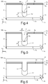
- Figures 1-13 illustrate, in lateral sectional view, manufacturing steps for the production of a semiconductor electronic device with trench region, according to an embodiment of the present invention.
- a power device in particular a MOS transistor with source electrode on a front side of the device, drain electrode on a back side of the device, and trench gate, which extends from the front side towards the back side.
- Figures 1-13 illustrate the electronic device in lateral sectional view, in a system of spatial coordinates defined by mutually orthogonal axes X, Y, and Z.
- the present disclosure describes exclusively the manufacturing steps of interest for the invention (i.e., regarding construction of a trench gate provided with an internal insulation region). Further elements of the electronic device (e.g., edge regions or other structures), which are of a per se known type, are not described and illustrated here in the figures.
- Figure 1 illustrates a wafer 100 comprising a substrate 1, in particular of monocrystalline silicon, having a first conductivity (here, of an N type) and a first doping concentration (e.g., higher than 10 19 at./cm 3 ).
- the substrate 1 is delimited on a first side 1a and on a second side 1b opposite to one another along the axis Z.
- a structural layer or region 2 is formed, for example by epitaxial growth of silicon, having the first conductivity (N) and a concentration of dopants lower than that of the substrate 1 (e.g., comprised between 1.10 15 and 5.10 16 ions/cm 3 ).
- the structural region 2 has a thickness, along Z, that is chosen according to the need on the basis of the voltage class in which the electronic device is to operate, and is, for example, comprised approximately between 1.5 ⁇ m and 100 ⁇ m.
- the structural region 2 is delimited by a first side 2a and a second side 2b opposite to one another in the direction Z.
- the second side 2b of the structural region 2 coincides with the first side 1a of the substrate 1.
- one or more further structural regions which are, for example, grown epitaxially and are similar to the structural region 2, may be formed between the first side 1a of the substrate 1 and the second side 2b of the structural region 2.
- a mask multilayer 4 is then formed, which includes: a first mask layer 4a, in contact with the first side 2a, made, for example, of silicon oxide grown via thermal oxidation with a thickness comprised between 5 nm and 100 nm; a second mask layer 4b, immediately on top of the first mask layer 4a, made, for example, of silicon nitride with a thickness comprised between 10 nm and 1 ⁇ m; and a third mask layer 4c, immediately on top of the second mask layer 4b, made, for example, of TEOS or photoresist with a thickness comprised between 10 nm and 10 ⁇ m.
- the first mask layer 4a has the function of forming an interface between the structural layer 2, of silicon, and the second mask layer 4b, of silicon nitride, in order to prevent mechanical stress induced by silicon nitride and prevent nitriding of the surface of the silicon itself, which jeopardises operation of the device.
- the second mask layer 4b forms a hard mask for a subsequent step of etching of the structural layer 2.
- the third mask layer 4c forms a further hard mask for the step of etching of the structural layer 2.
- the mask multilayer 4 is removed in regions of the wafer 100 where the trench gate is to be formed. Then etching is carried out, in particular of a dry type, for example RIE, for selective removal of portions of the structural layer 2 exposed through the mask multilayer 4 and so as to form a trench 6 delimited by a bottom wall 6a and side walls 6b.
- the trench 6 has a depth, measured starting from the first side 2a of the structural layer 2 comprised, for example, between 1 and 2 ⁇ m.
- the trench 6 may be strip-shaped, with main extension along the axis Y ranging from a few microns to a few millimetres, and a width, along the axis X, comprised between 0.5 ⁇ m and 1.5 ⁇ m.
- Other layouts may be envisaged for the trench 6; for example, it may have, once again in view in the plane XY, a circular shape with a diameter comprised between 0.5 ⁇ m and 1.5 ⁇ m, or some other shape, for example, generically polygonal.
- an implanted region 8 having a second conductivity type (here, a conductivity of P+ type), for example by a step of ion implantation of boron. More in particular, a plurality of successive implantations (e.g., from one to three implantations) are carried out, each at a respective implantation energy but with the same dose of dopant atoms (or respective doses chosen in a limited range, for example not more than one order of magnitude).
- the implanted region 8 is thus formed, which extends from the bottom wall 6a of the trench 6 for a depth d 1 , measured starting from the bottom wall 6a, of a few microns.
- the implantation dose is, by way of example, comprised between 5 ⁇ 10 14 and 5 ⁇ 10 15 at./cm 3, and the implantation energies are, by way of example, comprised between 100 keV and 1000 keV.
- a subsequent rapid thermal process at a high temperature (also known as RTA or RTP), for example, comprised between 900°C and 1150°C for 30 seconds, activates the dopants of the implanted region 8 and enables minimal diffusion thereof in the structural layer 2, in particular in depth.
- a doped region 10 is thus formed ( Figure 3 ), having an extension d 2 , measured starting from the bottom wall 6a, just a little greater than d 1 and of a few microns.
- the doped region 10 is converted into a porous-silicon region 12.
- porous silicon presents as an interconnected network of pores.
- the size, direction, position, and depth of the pores depend upon parameters set during formation thereof, as well as upon the conductivity type of the region in which the porous silicon is formed.
- the morphology of porous silicon differs.
- the mean diameter of the pores ranges between 1 nm and 100 nm, and the structure obtained is branched, highly interconnected, and homogeneous.
- the dose of dopant for formation of the doped region 10 increases, the diameter of the pores and the distance between them increase.
- the implantation dose affects both the rate of growth of porous silicon and the degree of porosity (in particular, the higher the dose of dopants, the greater the volume of the voids at the expense of the volume of full silicon).
- the system used, for anodic etching of silicon typically comprises a cell with three electrodes, one of which is represented by the crystalline-silicon wafer 100, which contains an aqueous electrolytic solution.
- the wafer 100 is located at a positive (anode) potential with respect to the electrolytic solution; the front side of the wafer 100 (having the trench 6) is arranged directly in contact with the electrolytic solution.
- the electrolytic solution is typically made up of HF, de-ionised water, and ethanol. Other compounds may be used to improve wettability of the silicon surface exposed to etching, reducing the formation of hydrogen bubbles that are formed, during the electrochemical reaction, at the electrodes.
- the characteristics of the porous-silicon region 12 that is to be formed depend markedly upon the parameters set during the etching step, in particular upon:
- the reaction of dissolution occurs immediately for the silicon regions of a P type, which may be anodised in the dark. Instead, for N-type silicon the presence of lighting is necessary. It is thus possible to form the porous-silicon region selectively in the implanted region 10.
- the holes are necessary for the chemical reaction of dissolution of the crystalline silicon, which takes place at the interface between the silicon and the electrolytic solution.
- the step of Figure 5 is carried out, in which the porous-silicon region 12 is transformed into a dielectric region 14, in particular of silicon oxide.
- porous-silicon region 12 enables transformation thereof with extreme ease into silicon oxide (also known as PSO, Porous Silicon Oxide).
- silicon oxide also known as PSO, Porous Silicon Oxide.
- Porous silicon presents, in fact, a high oxidation rate at low temperatures, an oxidation rate much higher than that of monocrystalline silicon. This is basically due to an extensive surface exposed to the process, which enables layers of porous silicon oxide to be obtained with a large thickness in a relatively short time.
- a process of oxidation is carried out in a furnace at a high temperature (e.g., a rapid thermal process, at a temperature of 1000°C with a temperature ascending ramp in an interval of 5-30 s, maintenance at the temperature in an interval of 1-10 min, and decrease to room temperature with a descending ramp down to room temperature in an interval of 30-60 s).
- This rapid-thermal-oxidation (RTO) process transforms the porous-silicon region 12 into the dielectric region 14, of low-density silicon oxide.
- the thermal-oxidation process mentioned here likewise causes formation of an oxide layer on the side walls 6b of the trench 6, with a thickness d 3 , measured along the axis X, of a few nanometers. Consequently, the internal free volume of the trench 6 is reduced.
- a step of formation for example via CVD, of a layer of dielectric material 16 having a density higher than the density of the dielectric region 14, made, for example, of TEOS (alternatively, BPSG, USG, and SOG may be chosen), until the trench 6 is completely filled.
- the layer of dielectric material 16 fills the trench 6 and likewise deposits on the wafer 100.
- anisotropic plasma chemical etching is carried out for progressive removal of the layer of dielectric material 16 and of the third mask layer 4c (both of which are of TEOS in this example), as far as the second mask layer 4b, here of Si 3 N 4 , which functions as etch-stop layer.
- a portion 16' of the layer of dielectric material 16 remains inside the trench 6, on the bottom side 6a, to cover completely, and protect, the dielectric region 14.
- etch in HF (wet etch) is made to complete removal of any possible oxide still present on the inner walls 6b of the trench 6.
- the gate-oxide layer 20 has, for example, a thickness comprised between 10 and 50 nm.
- a layer of doped polysilicon 22, having the first conductivity type (N), and a doping level comprised between 10 17 at./cm 3 and 10 19 at./cm 3 is deposited, and ( Figure 11 ), a subsequent etching step is carried out for removal of the layer of doped polysilicon 22 from the front of the wafer 100 except for the trench 6.
- a trench conductive region 24, here of doped polysilicon N extends in the trench 6 on the portion 16', filling the trench 6 completely.
- the trench conductive region 24 fills the trench 6 only partially, stopping at a distance from the first side 2a, measured along Z, comprised between 100 nm and the depth of the trench 6.
- the trench conductive region 24 forms, at least in part, the gate electrode, which is electrically insulated from the structural layer 2 by the gate-oxide layer 20 (gate dielectric).
- Processing of the wafer 100 may then continue ( Figure 13 ) with deposition of pre-metallization dielectric 33, etching of the latter for opening electrical contacts by photolithography so as to reach and expose respective surface portions of the gate electrode 24 and of the source regions 32, respective depositions of one or more metal layers that contact the gate electrode 24 and the source regions 32, and photolithographic definition of said metal layers 36 for completing formation of the source and gate electrodes (the cross-sectional view of Figure 13 represents exclusively the gate metallization 36).
- a further deposition on the back of the wafer (on the second side 1b of the substrate 1) enables formation of a drain metallization 38.
- the body region 30 is formed by implanting dopant species of a P type in order to obtain a doping level comprised approximately between 1 ⁇ 10 17 ions/cm 3 and 5.10 17 ions/cm 3 .
- the body region 30 is formed in the structural region 2 for a depth in the direction Z comprised, for example, approximately between 0.5 ⁇ m and 1.0 ⁇ m.
- the source regions 32 extend in the body region 30, facing the first side 2a of the structural region 2, for a depth in the direction Z comprised, for example, approximately between 100 nm and 150 nm.
- the source regions 32 each have a doping level, for example, of approximately 1 ⁇ 10 20 ions/cm 3 , and extend in top plan view, alongside the gate electrode 24, separated from the latter by the dielectric 20.
- the gate and source metallizations 36 are formed by depositing conductive material on the wafer 100, in particular metal such as aluminium.
- the drain metallization 38 is formed by a step of deposition of conductive material, in particular metal, on the back of the wafer 100, thus completing formation of the drain terminal.
- a vertical-conduction electronic device here, a power MOSFET 40 is thus formed.
- an electric current may flow vertically (along Z) from the source regions 32 to the drain metallization 38, through the structural region 2 and the substrate 1.
- the electronic device 40 is, by way of example, one of the following: a vertical-conduction power MOS transistor, a power IGBT, or an MCT (MOS-Controlled Thyristor). Other applications may be envisaged, according to need.
- said dielectric region 14 has a low value of dielectric constant, which enables reduction of the parasitic capacitance between the conductive polysilicon region 24 (gate) and the portion of the structural layer 2 that extends underneath the dielectric region 14.
- the technical solution according to the present invention is likewise reliable, in so far as porous silicon oxide does not generate a significant stress at the interface with the structural layer 2. Consequently, no significant drifts of operating parameters or structural damages to the electronic device thus manufactured are noted during its service life.
- the process according to the present invention is flexible, in so far as the depth that may be reached by the dielectric region 14 may be adjusted during the step of implantation and diffusion of the implanted region 10.
- the present invention may be adapted for manufacturing an electronic device different from what is illustrated in the figures (for example, comprising a different configuration of the body region and/or of the source regions).
Landscapes
- Electrodes Of Semiconductors (AREA)
- Formation Of Insulating Films (AREA)
- Insulated Gate Type Field-Effect Transistor (AREA)
- Pressure Sensors (AREA)
Abstract
Description
- The present invention relates to a semiconductor electronic device with trench gate and to a method for manufacturing the semiconductor electronic device with trench gate.
- Vertical-conduction power MOSFETs are known that have a buried-gate region or trench-gate region.
- For instance, the patent document No.
US 2015/0206968 describes a vertical-channel LDMOS semiconductor device, in which a gate trench extends in depth in a semiconductor body and comprises a conductive region, of doped polysilicon, surrounded and electrically insulated from the semiconductor body by a dielectric region (made, for example, of silicon oxide or silicon nitride). - The dielectric region may be formed by a process of deposition, for example liquid-phase deposition (LPD), or else by thermal growth of an oxide. Both of the processes present some intrinsic limits. For instance, deposition of a dielectric layer may cause crystallographic interface stresses that may jeopardise electrical operation of the device (e.g., generating traps for the charge carriers), whereas thermal growth requires the use of structures for protecting the surface regions in which growth of a thermal oxide is undesirable or counterproductive.
- Consequently, there is the need for a process for manufacturing an electronic device with trench gate that will overcome the disadvantages of the prior art.
- According to the present invention, a semiconductor electronic device and a method for manufacturing the semiconductor electronic device are provided, as defined in the annexed claims.
- For a better understanding of the present invention, preferred embodiments thereof are now described, purely by way of non-limiting example, with reference to the attached drawings, wherein
Figures 1-13 illustrate, in lateral sectional view, manufacturing steps for the production of a semiconductor electronic device with trench region, according to an embodiment of the present invention. - According to the present invention, a power device is provided, in particular a MOS transistor with source electrode on a front side of the device, drain electrode on a back side of the device, and trench gate, which extends from the front side towards the back side.
- The steps for manufacturing the electronic device according to the present invention are described in the following, with reference to
Figures 1-13. Figures 1-13 illustrate the electronic device in lateral sectional view, in a system of spatial coordinates defined by mutually orthogonal axes X, Y, and Z. - In particular, the present disclosure describes exclusively the manufacturing steps of interest for the invention (i.e., regarding construction of a trench gate provided with an internal insulation region). Further elements of the electronic device (e.g., edge regions or other structures), which are of a per se known type, are not described and illustrated here in the figures.
-
Figure 1 illustrates awafer 100 comprising asubstrate 1, in particular of monocrystalline silicon, having a first conductivity (here, of an N type) and a first doping concentration (e.g., higher than 1019 at./cm3). Thesubstrate 1 is delimited on afirst side 1a and on asecond side 1b opposite to one another along the axis Z. - On the
substrate 1, a structural layer orregion 2 is formed, for example by epitaxial growth of silicon, having the first conductivity (N) and a concentration of dopants lower than that of the substrate 1 (e.g., comprised between 1.1015 and 5.1016 ions/cm3). Thestructural region 2 has a thickness, along Z, that is chosen according to the need on the basis of the voltage class in which the electronic device is to operate, and is, for example, comprised approximately between 1.5 µm and 100 µm. - The
structural region 2 is delimited by afirst side 2a and asecond side 2b opposite to one another in the direction Z. Thesecond side 2b of thestructural region 2 coincides with thefirst side 1a of thesubstrate 1. - According to alternative embodiments (not illustrated), one or more further structural regions, which are, for example, grown epitaxially and are similar to the
structural region 2, may be formed between thefirst side 1a of thesubstrate 1 and thesecond side 2b of thestructural region 2. - On the
first side 2a of thestructural layer 2, amask multilayer 4 is then formed, which includes: afirst mask layer 4a, in contact with thefirst side 2a, made, for example, of silicon oxide grown via thermal oxidation with a thickness comprised between 5 nm and 100 nm; asecond mask layer 4b, immediately on top of thefirst mask layer 4a, made, for example, of silicon nitride with a thickness comprised between 10 nm and 1 µm; and athird mask layer 4c, immediately on top of thesecond mask layer 4b, made, for example, of TEOS or photoresist with a thickness comprised between 10 nm and 10 µm. Thefirst mask layer 4a has the function of forming an interface between thestructural layer 2, of silicon, and thesecond mask layer 4b, of silicon nitride, in order to prevent mechanical stress induced by silicon nitride and prevent nitriding of the surface of the silicon itself, which jeopardises operation of the device. Thesecond mask layer 4b forms a hard mask for a subsequent step of etching of thestructural layer 2. Thethird mask layer 4c forms a further hard mask for the step of etching of thestructural layer 2. - By photolithographic technique, the
mask multilayer 4 is removed in regions of thewafer 100 where the trench gate is to be formed. Then etching is carried out, in particular of a dry type, for example RIE, for selective removal of portions of thestructural layer 2 exposed through themask multilayer 4 and so as to form atrench 6 delimited by abottom wall 6a andside walls 6b. Thetrench 6 has a depth, measured starting from thefirst side 2a of thestructural layer 2 comprised, for example, between 1 and 2 µm. - In top plan view, in the plane XY, the
trench 6 may be strip-shaped, with main extension along the axis Y ranging from a few microns to a few millimetres, and a width, along the axis X, comprised between 0.5 µm and 1.5 µm. Other layouts may be envisaged for thetrench 6; for example, it may have, once again in view in the plane XY, a circular shape with a diameter comprised between 0.5 µm and 1.5 µm, or some other shape, for example, generically polygonal. - Next (
Figure 2 ), at thebottom wall 6a of thetrench 6, it is formed an implantedregion 8 having a second conductivity type (here, a conductivity of P+ type), for example by a step of ion implantation of boron. More in particular, a plurality of successive implantations (e.g., from one to three implantations) are carried out, each at a respective implantation energy but with the same dose of dopant atoms (or respective doses chosen in a limited range, for example not more than one order of magnitude). The implantedregion 8 is thus formed, which extends from thebottom wall 6a of thetrench 6 for a depth d1, measured starting from thebottom wall 6a, of a few microns. The implantation dose is, by way of example, comprised between 5·1014 and 5·1015 at./cm3, and the implantation energies are, by way of example, comprised between 100 keV and 1000 keV. - A subsequent rapid thermal process at a high temperature (also known as RTA or RTP), for example, comprised between 900°C and 1150°C for 30 seconds, activates the dopants of the implanted
region 8 and enables minimal diffusion thereof in thestructural layer 2, in particular in depth. Adoped region 10 is thus formed (Figure 3 ), having an extension d2, measured starting from thebottom wall 6a, just a little greater than d1 and of a few microns. - As an alternative to RTA or RTP, it is possible to carry out an oxidation process of an ISSG type or, once again alternatively, an oxidation (of a wet or dry type) in an oven.
- Next (
Figure 4 ), thedoped region 10 is converted into a porous-silicon region 12. - In general, the structure of porous silicon, from a morphological standpoint, presents as an interconnected network of pores. The size, direction, position, and depth of the pores depend upon parameters set during formation thereof, as well as upon the conductivity type of the region in which the porous silicon is formed.
- In fact, as is known, on the basis of the density and type of doping of the region in which the porous silicon is formed, the morphology of porous silicon differs. In the context of the present disclosure, according to the embodiment discussed previously, in the case of silicon of a P type, the mean diameter of the pores ranges between 1 nm and 100 nm, and the structure obtained is branched, highly interconnected, and homogeneous. As the dose of dopant for formation of the
doped region 10 increases, the diameter of the pores and the distance between them increase. The present applicant has noted that the implantation dose affects both the rate of growth of porous silicon and the degree of porosity (in particular, the higher the dose of dopants, the greater the volume of the voids at the expense of the volume of full silicon). - The system used, for anodic etching of silicon, typically comprises a cell with three electrodes, one of which is represented by the crystalline-
silicon wafer 100, which contains an aqueous electrolytic solution. - The
wafer 100 is located at a positive (anode) potential with respect to the electrolytic solution; the front side of the wafer 100 (having the trench 6) is arranged directly in contact with the electrolytic solution. The electrolytic solution is typically made up of HF, de-ionised water, and ethanol. Other compounds may be used to improve wettability of the silicon surface exposed to etching, reducing the formation of hydrogen bubbles that are formed, during the electrochemical reaction, at the electrodes. - The characteristics of the porous-
silicon region 12 that is to be formed (size of the pores, direction, porosity) depend markedly upon the parameters set during the etching step, in particular upon: - the composition of the electrolyte in solution, and thus the percentage of HF present in solution, chosen between 5% and 48%;
- the value of the anodisation current, chosen between 5 and 1000 mA/cm2;
- the etching time, chosen between 5 and 500 s;
- the resistivity of the substrate (i.e., doping, already discussed previously); and
- the temperature of the solution during the process, here carried out at room temperature.
- The reaction of dissolution occurs immediately for the silicon regions of a P type, which may be anodised in the dark. Instead, for N-type silicon the presence of lighting is necessary. It is thus possible to form the porous-silicon region selectively in the implanted
region 10. The holes are necessary for the chemical reaction of dissolution of the crystalline silicon, which takes place at the interface between the silicon and the electrolytic solution. - Then, the step of
Figure 5 is carried out, in which the porous-silicon region 12 is transformed into adielectric region 14, in particular of silicon oxide. - The porous nature of the porous-
silicon region 12 enables transformation thereof with extreme ease into silicon oxide (also known as PSO, Porous Silicon Oxide). Porous silicon presents, in fact, a high oxidation rate at low temperatures, an oxidation rate much higher than that of monocrystalline silicon. This is basically due to an extensive surface exposed to the process, which enables layers of porous silicon oxide to be obtained with a large thickness in a relatively short time. - For this purpose, a process of oxidation is carried out in a furnace at a high temperature (e.g., a rapid thermal process, at a temperature of 1000°C with a temperature ascending ramp in an interval of 5-30 s, maintenance at the temperature in an interval of 1-10 min, and decrease to room temperature with a descending ramp down to room temperature in an interval of 30-60 s). This rapid-thermal-oxidation (RTO) process transforms the porous-
silicon region 12 into thedielectric region 14, of low-density silicon oxide. - The thermal-oxidation process mentioned here likewise causes formation of an oxide layer on the
side walls 6b of thetrench 6, with a thickness d3, measured along the axis X, of a few nanometers. Consequently, the internal free volume of thetrench 6 is reduced. - This is followed (
Figure 6 ) by a step of formation, for example via CVD, of a layer ofdielectric material 16 having a density higher than the density of thedielectric region 14, made, for example, of TEOS (alternatively, BPSG, USG, and SOG may be chosen), until thetrench 6 is completely filled. The layer ofdielectric material 16 fills thetrench 6 and likewise deposits on thewafer 100. - Next (
Figure 7 ), anisotropic plasma chemical etching is carried out for progressive removal of the layer ofdielectric material 16 and of thethird mask layer 4c (both of which are of TEOS in this example), as far as thesecond mask layer 4b, here of Si3N4, which functions as etch-stop layer. A portion 16' of the layer ofdielectric material 16 remains inside thetrench 6, on thebottom side 6a, to cover completely, and protect, thedielectric region 14. - Optionally, a further etch in HF (wet etch) is made to complete removal of any possible oxide still present on the
inner walls 6b of thetrench 6. - Then (
Figure 8 ), two selective chemical etches are made for respective removal of thesecond mask layer 4b and the firstunderlying mask layer 4a, until thefirst side 2a of thestructural layer 2 is exposed. - There then follows (
Figure 9 ) a step of formation, for example by thermal oxidation, of a gate-oxide layer 20 on theside walls 6b of the trench 6 (i.e., at the interface with thestructural layer 2 exposed inside the trench 6) and on thefirst side 2a of thestructural layer 2. The gate-oxide layer 20 has, for example, a thickness comprised between 10 and 50 nm. - Next (
Figure 10 ), a layer of dopedpolysilicon 22, having the first conductivity type (N), and a doping level comprised between 1017 at./cm3 and 1019 at./cm3 is deposited, and (Figure 11 ), a subsequent etching step is carried out for removal of the layer of dopedpolysilicon 22 from the front of thewafer 100 except for thetrench 6. In other words, a trenchconductive region 24, here of doped polysilicon N, extends in thetrench 6 on the portion 16', filling thetrench 6 completely. - In a different embodiment, not illustrated, the trench
conductive region 24 fills thetrench 6 only partially, stopping at a distance from thefirst side 2a, measured along Z, comprised between 100 nm and the depth of thetrench 6. - The trench
conductive region 24 forms, at least in part, the gate electrode, which is electrically insulated from thestructural layer 2 by the gate-oxide layer 20 (gate dielectric). - Then, with reference to
Figure 12 , formed with known techniques of implantation of dopant species and diffusion are abody region 30, having the second conductivity (P), and one ormore source regions 32, having the first conductivity (N), which are self-aligned to the trench 6 (here filled as described previously) . - Processing of the
wafer 100 may then continue (Figure 13 ) with deposition of pre-metallization dielectric 33, etching of the latter for opening electrical contacts by photolithography so as to reach and expose respective surface portions of thegate electrode 24 and of thesource regions 32, respective depositions of one or more metal layers that contact thegate electrode 24 and thesource regions 32, and photolithographic definition of said metal layers 36 for completing formation of the source and gate electrodes (the cross-sectional view ofFigure 13 represents exclusively the gate metallization 36). A further deposition on the back of the wafer (on thesecond side 1b of the substrate 1) enables formation of adrain metallization 38. - In detail, the
body region 30 is formed by implanting dopant species of a P type in order to obtain a doping level comprised approximately between 1·1017 ions/cm3 and 5.1017 ions/cm3. In greater detail, thebody region 30 is formed in thestructural region 2 for a depth in the direction Z comprised, for example, approximately between 0.5 µm and 1.0 µm. - The
source regions 32 extend in thebody region 30, facing thefirst side 2a of thestructural region 2, for a depth in the direction Z comprised, for example, approximately between 100 nm and 150 nm. Thesource regions 32 each have a doping level, for example, of approximately 1·1020 ions/cm3, and extend in top plan view, alongside thegate electrode 24, separated from the latter by the dielectric 20. - The gate and source metallizations 36 are formed by depositing conductive material on the
wafer 100, in particular metal such as aluminium. Likewise, also thedrain metallization 38 is formed by a step of deposition of conductive material, in particular metal, on the back of thewafer 100, thus completing formation of the drain terminal. - A vertical-conduction electronic device (here, a power MOSFET) 40 is thus formed. Thus, in use, an electric current may flow vertically (along Z) from the
source regions 32 to thedrain metallization 38, through thestructural region 2 and thesubstrate 1. - The
electronic device 40 according to the present invention is, by way of example, one of the following: a vertical-conduction power MOS transistor, a power IGBT, or an MCT (MOS-Controlled Thyristor). Other applications may be envisaged, according to need. - From an examination of the characteristics of the disclosure provided according to the present invention the advantages that it affords are evident.
- In particular, formation of the
dielectric region 14 by oxidation of porous silicon is fast and far from costly, and considerably simplifies the manufacturing processes according to the prior art. - Further, said
dielectric region 14 has a low value of dielectric constant, which enables reduction of the parasitic capacitance between the conductive polysilicon region 24 (gate) and the portion of thestructural layer 2 that extends underneath thedielectric region 14. - The technical solution according to the present invention is likewise reliable, in so far as porous silicon oxide does not generate a significant stress at the interface with the
structural layer 2. Consequently, no significant drifts of operating parameters or structural damages to the electronic device thus manufactured are noted during its service life. - Finally, the process according to the present invention is flexible, in so far as the depth that may be reached by the
dielectric region 14 may be adjusted during the step of implantation and diffusion of the implantedregion 10. - Finally, it is clear that modifications and variations may be made to what has been described and illustrated herein, without thereby departing from the scope of the present invention, as defined in the annexed claims.
- In particular, the present invention may be adapted for manufacturing an electronic device different from what is illustrated in the figures (for example, comprising a different configuration of the body region and/or of the source regions).
Claims (14)
- A semiconductor electronic device (40) comprising:- a semiconductor body (1, 2), having a first conductivity, delimited by a first side (2a) and a second side (1b) opposite to one another along an axis (Z);- a body region (30), having a second conductivity opposite to the first conductivity, in the semiconductor body (1, 2) facing the first side (2a);- a source terminal (32), having the first conductivity, extending at least in part in the body region (30) ;- a drain terminal (38), having the first conductivity, extending at the second side (1b) of the semiconductor body (1, 2); and- a trench gate (6, 14, 16', 24), which extends in the semiconductor body (1, 2) from the first side (2a) towards the second side (1b), through the body region (30) and the source region (32),characterized in that said trench gate (6, 14, 16', 24) includes a dielectric region (14) of porous silicon oxide buried in the semiconductor body (1, 2), and a gate conductive region (24) extending between the dielectric region (14) of porous silicon oxide and said first side (2a).
- The device according to claim 1, further comprising a gate dielectric (20) extending between the gate conductive region (24) and the semiconductor body (1, 2).
- The device according to claim 1 or claim 2, wherein said trench gate (6, 14, 16', 24) further includes a protection region (16') between the dielectric region (14) of porous silicon oxide and the gate conductive region (24), designed for separating the dielectric region (14) of porous silicon oxide from the gate conductive region (24).
- The device according to claim 3, wherein the protection region (16') is of an electrically insulating material.
- The device according to any one of the preceding claims, wherein the gate conductive region (24) is of doped polysilicon.
- The device according to any one of the preceding claims, chosen in the group comprising: a vertical-conduction power MOS transistor, a power IGBT, and an MCT.
- A method for manufacturing a semiconductor electronic device (40), comprising the steps of:- forming, at a first side (2a) of a semiconductor body (1, 2) having a first conductivity (N), a body region (30) having a second conductivity (P) opposite to the first conductivity;- forming, at least in part in the body region (30), a source terminal (32) having the first conductivity (N);- forming, at a second side (1b), opposite to the first side (2a), of the semiconductor body (1, 2), a drain terminal (38); and- forming a trench (6) at the first side (2a) of the semiconductor body (1, 2) and through the body region (30) and the source region (32),characterized by further comprises the steps of:forming a porous-silicon region (12) in the semiconductor body (1, 2) at a bottom side (6a) of the trench (6) and in spatial continuation of the trench (6); andoxidising the porous-silicon region (12), to form a dielectric region (14) of porous silicon oxide.
- The method according to claim 7, wherein the step of forming the porous-silicon region (12) comprises:implanting dopant species that have the second conductivity (P) in the semiconductor body (1, 2), at the bottom side (6a) of the trench (6);thermally activating said implanted dopant species, to form an implanted region (10); andcarrying out an electrochemical reaction designed to transform said implanted region (10) into the porous-silicon region (12).
- The method according to claim 8, wherein said step of implanting dopant species includes carrying out a plurality of successive implantations with different implantation energies in the range comprised between 100 keV and 1000 keV and with the same implantation dose comprised between 5·1014 and 5·1015 at./cm3.
- The method according to claim 8 or claim 9, wherein the step of carrying out the electrochemical reaction comprises the substeps of:inserting said semiconductor body (1, 2) in an aqueous electrolytic solution that includes hydrofluoric acid in a percentage comprised between 5% and 48%;maintaining the electrolytic solution at room temperature; andapplying an anodization current having a value comprised between 5 mA/cm2 and 1000 mA/cm2.
- The method according to any one of claims 8 to 10, wherein the step of forming the porous-silicon region (12) further comprises carrying out a thermal-oxidation process at a temperature comprised between 900°C and 1050°C, with an ascending ramp in temperature in an interval of 5 to 60 s, and maintenance of constant temperature in an interval of 1 to 10 min.
- The method according to any one of claims 7 to 11, further comprising the step of forming a gate dielectric (20) at side walls (6b) of the trench (6), configured to insulate the gate conductive region (24) from the semiconductor body (1, 2).
- The method according to any one of claims 7 to 12, further comprising the step of forming a protection region (16') on the dielectric region (14) of porous silicon oxide,
and wherein the step of forming the gate conductive region (24) comprises forming the gate conductive region (24) on the protection region (16') so that the gate conductive region (24) is separated from the dielectric region (14) of porous silicon oxide by the protection region (16'). - The method according to claim 13, wherein the step of forming the protection region (16') comprises depositing insulating material in the trench (6).
Applications Claiming Priority (1)
| Application Number | Priority Date | Filing Date | Title |
|---|---|---|---|
| IT201800000928A IT201800000928A1 (en) | 2018-01-15 | 2018-01-15 | SEMICONDUCTOR ELECTRONIC DEVICE WITH TRENCH DOOR AND RELATIVE MANUFACTURING METHOD |
Publications (2)
| Publication Number | Publication Date |
|---|---|
| EP3511988A1 true EP3511988A1 (en) | 2019-07-17 |
| EP3511988B1 EP3511988B1 (en) | 2021-12-01 |
Family
ID=61731794
Family Applications (1)
| Application Number | Title | Priority Date | Filing Date |
|---|---|---|---|
| EP19151957.8A Active EP3511988B1 (en) | 2018-01-15 | 2019-01-15 | Semiconductor electronic device with trench gate and manufacturing method thereof |
Country Status (4)
| Country | Link |
|---|---|
| US (1) | US20190221652A1 (en) |
| EP (1) | EP3511988B1 (en) |
| CN (2) | CN209496879U (en) |
| IT (1) | IT201800000928A1 (en) |
Cited By (1)
| Publication number | Priority date | Publication date | Assignee | Title |
|---|---|---|---|---|
| EP4092753A1 (en) * | 2021-05-21 | 2022-11-23 | Nexperia B.V. | Trench mosfet |
Families Citing this family (2)
| Publication number | Priority date | Publication date | Assignee | Title |
|---|---|---|---|---|
| IT201800000928A1 (en) * | 2018-01-15 | 2019-07-15 | St Microelectronics Srl | SEMICONDUCTOR ELECTRONIC DEVICE WITH TRENCH DOOR AND RELATIVE MANUFACTURING METHOD |
| IT202300026448A1 (en) * | 2023-12-12 | 2025-06-12 | St Microelectronics Int Nv | METHOD OF MANUFACTURING A SEMICONDUCTOR ELECTRONIC DEVICE WITH A TRENCH GATE |
Citations (4)
| Publication number | Priority date | Publication date | Assignee | Title |
|---|---|---|---|---|
| EP0205639A1 (en) * | 1985-06-25 | 1986-12-30 | Eaton Corporation | Bidirectional power fet with substrate referenced shield |
| WO2004055883A1 (en) * | 2002-12-14 | 2004-07-01 | Koninklijke Philips Electronics N.V. | Method of manufacture of a trench-gate semiconductor device |
| US20150206968A1 (en) | 2014-01-21 | 2015-07-23 | Stmicroelectronics S.R.L. | Power ldmos semiconductor device with reduced on-resistance and manufacturing method thereof |
| US20150333140A1 (en) * | 2014-05-15 | 2015-11-19 | Maxchip Electronics Corp. | Semiconductor structure and method of forming the same |
Family Cites Families (9)
| Publication number | Priority date | Publication date | Assignee | Title |
|---|---|---|---|---|
| US4643804A (en) * | 1985-07-25 | 1987-02-17 | At&T Bell Laboratories | Forming thick dielectric at the bottoms of trenches utilized in integrated-circuit devices |
| DE69941456D1 (en) * | 1999-12-31 | 2009-11-05 | St Microelectronics Srl | Production process of an SOI wafer |
| KR100510772B1 (en) * | 2003-02-04 | 2005-08-30 | 동부아남반도체 주식회사 | Formation method of silicon on insulator substrate for semiconductor |
| US7067387B2 (en) * | 2003-08-28 | 2006-06-27 | Taiwan Semiconductor Manufacturing Company | Method of manufacturing dielectric isolated silicon structure |
| US7566482B2 (en) * | 2003-09-30 | 2009-07-28 | International Business Machines Corporation | SOI by oxidation of porous silicon |
| US7659581B2 (en) * | 2005-11-30 | 2010-02-09 | International Business Machines Corporation | Transistor with dielectric stressor element fully underlying the active semiconductor region |
| US8384152B2 (en) * | 2007-09-20 | 2013-02-26 | Rohm Co., Ltd. | Semiconductor device having trench gate VDMOSFET and method of manufacturing the same |
| CN102456736A (en) * | 2010-10-29 | 2012-05-16 | 上海宏力半导体制造有限公司 | Channel-type field effect tube and preparation method thereof |
| IT201800000928A1 (en) * | 2018-01-15 | 2019-07-15 | St Microelectronics Srl | SEMICONDUCTOR ELECTRONIC DEVICE WITH TRENCH DOOR AND RELATIVE MANUFACTURING METHOD |
-
2018
- 2018-01-15 IT IT201800000928A patent/IT201800000928A1/en unknown
-
2019
- 2019-01-14 US US16/247,358 patent/US20190221652A1/en not_active Abandoned
- 2019-01-14 CN CN201920057398.0U patent/CN209496879U/en active Active
- 2019-01-14 CN CN201910033481.9A patent/CN110047929B/en active Active
- 2019-01-15 EP EP19151957.8A patent/EP3511988B1/en active Active
Patent Citations (4)
| Publication number | Priority date | Publication date | Assignee | Title |
|---|---|---|---|---|
| EP0205639A1 (en) * | 1985-06-25 | 1986-12-30 | Eaton Corporation | Bidirectional power fet with substrate referenced shield |
| WO2004055883A1 (en) * | 2002-12-14 | 2004-07-01 | Koninklijke Philips Electronics N.V. | Method of manufacture of a trench-gate semiconductor device |
| US20150206968A1 (en) | 2014-01-21 | 2015-07-23 | Stmicroelectronics S.R.L. | Power ldmos semiconductor device with reduced on-resistance and manufacturing method thereof |
| US20150333140A1 (en) * | 2014-05-15 | 2015-11-19 | Maxchip Electronics Corp. | Semiconductor structure and method of forming the same |
Non-Patent Citations (1)
| Title |
|---|
| R. HERINO: "Porosity and Pore Size Distributions of Porous Silicon Layers", JOURNAL OF THE ELECTROCHEMICAL SOCIETY, vol. 134, no. 8, 1 January 1987 (1987-01-01), pages 1994, XP055503498, ISSN: 0013-4651, DOI: 10.1149/1.2100805 * |
Cited By (2)
| Publication number | Priority date | Publication date | Assignee | Title |
|---|---|---|---|---|
| EP4092753A1 (en) * | 2021-05-21 | 2022-11-23 | Nexperia B.V. | Trench mosfet |
| US12342569B2 (en) | 2021-05-21 | 2025-06-24 | Nexperia B.V. | Trench MOSFET |
Also Published As
| Publication number | Publication date |
|---|---|
| US20190221652A1 (en) | 2019-07-18 |
| CN110047929B (en) | 2023-04-18 |
| CN110047929A (en) | 2019-07-23 |
| EP3511988B1 (en) | 2021-12-01 |
| CN209496879U (en) | 2019-10-15 |
| IT201800000928A1 (en) | 2019-07-15 |
Similar Documents
| Publication | Publication Date | Title |
|---|---|---|
| CN112310194B (en) | Charge-balanced power devices and methods for manufacturing charge-balanced power devices | |
| TWI542009B (en) | Termination trench for power MOSFET applications and method of making same | |
| CN102270660B (en) | Method for forming trench type metal oxide semiconductor field effect transistor | |
| TWI773605B (en) | Method for manufacturing trench mosfet | |
| JP2004538648A (en) | MIS device having trench gate electrode and method of manufacturing the same | |
| WO2007001988A2 (en) | Structure and method for forming laterally extending dielectric layer in a trench-gate fet | |
| US20100003573A1 (en) | Method for processing portions of walls of an opening formed in a silicon substrate | |
| EP1733431A1 (en) | Trench semiconductor device and method of manufacturing it | |
| TWI761800B (en) | Trench type MOSFET device manufacturing method | |
| CN110896026A (en) | Trench MOSFET structure and method of making the same | |
| CN102969288B (en) | With the semiconductor device of imbedded electrode | |
| EP3511988B1 (en) | Semiconductor electronic device with trench gate and manufacturing method thereof | |
| CN107665922A (en) | Reverse blocking IGBT | |
| CN110429129A (en) | High pressure trench-type power semiconductor device and preparation method | |
| KR20190052971A (en) | Fabricating method for power semiconductor device and power semiconductor device thereof | |
| US12469706B2 (en) | Method for manufacturing trench-gate MOSFET | |
| CN111933529A (en) | Manufacturing method and structure of trench type MOSFET | |
| KR100584969B1 (en) | Semiconductor device and semiconductor device manufacturing method | |
| CN113921610A (en) | LDMOS device structure and manufacturing method thereof | |
| US7494876B1 (en) | Trench-gated MIS device having thick polysilicon insulation layer at trench bottom and method of fabricating the same | |
| CN113206148A (en) | Trench MOSFET and method of manufacturing the same | |
| US8999783B2 (en) | Method for producing a semiconductor device with a vertical dielectric layer | |
| CN117936381A (en) | Transistor device and method of processing a contactor for a semiconductor substrate | |
| EP3690952A1 (en) | Trench gate semiconductor device and method of manufacture | |
| CN216389378U (en) | Groove type power device |
Legal Events
| Date | Code | Title | Description |
|---|---|---|---|
| PUAI | Public reference made under article 153(3) epc to a published international application that has entered the european phase |
Free format text: ORIGINAL CODE: 0009012 |
|
| STAA | Information on the status of an ep patent application or granted ep patent |
Free format text: STATUS: THE APPLICATION HAS BEEN PUBLISHED |
|
| AK | Designated contracting states |
Kind code of ref document: A1 Designated state(s): AL AT BE BG CH CY CZ DE DK EE ES FI FR GB GR HR HU IE IS IT LI LT LU LV MC MK MT NL NO PL PT RO RS SE SI SK SM TR |
|
| AX | Request for extension of the european patent |
Extension state: BA ME |
|
| STAA | Information on the status of an ep patent application or granted ep patent |
Free format text: STATUS: REQUEST FOR EXAMINATION WAS MADE |
|
| 17P | Request for examination filed |
Effective date: 20191126 |
|
| RBV | Designated contracting states (corrected) |
Designated state(s): AL AT BE BG CH CY CZ DE DK EE ES FI FR GB GR HR HU IE IS IT LI LT LU LV MC MK MT NL NO PL PT RO RS SE SI SK SM TR |
|
| STAA | Information on the status of an ep patent application or granted ep patent |
Free format text: STATUS: EXAMINATION IS IN PROGRESS |
|
| 17Q | First examination report despatched |
Effective date: 20201008 |
|
| GRAP | Despatch of communication of intention to grant a patent |
Free format text: ORIGINAL CODE: EPIDOSNIGR1 |
|
| STAA | Information on the status of an ep patent application or granted ep patent |
Free format text: STATUS: GRANT OF PATENT IS INTENDED |
|
| INTG | Intention to grant announced |
Effective date: 20210623 |
|
| GRAS | Grant fee paid |
Free format text: ORIGINAL CODE: EPIDOSNIGR3 |
|
| GRAA | (expected) grant |
Free format text: ORIGINAL CODE: 0009210 |
|
| STAA | Information on the status of an ep patent application or granted ep patent |
Free format text: STATUS: THE PATENT HAS BEEN GRANTED |
|
| AK | Designated contracting states |
Kind code of ref document: B1 Designated state(s): AL AT BE BG CH CY CZ DE DK EE ES FI FR GB GR HR HU IE IS IT LI LT LU LV MC MK MT NL NO PL PT RO RS SE SI SK SM TR |
|
| REG | Reference to a national code |
Ref country code: GB Ref legal event code: FG4D |
|
| REG | Reference to a national code |
Ref country code: AT Ref legal event code: REF Ref document number: 1452630 Country of ref document: AT Kind code of ref document: T Effective date: 20211215 Ref country code: CH Ref legal event code: EP |
|
| REG | Reference to a national code |
Ref country code: IE Ref legal event code: FG4D |
|
| REG | Reference to a national code |
Ref country code: DE Ref legal event code: R096 Ref document number: 602019009590 Country of ref document: DE |
|
| REG | Reference to a national code |
Ref country code: LT Ref legal event code: MG9D |
|
| REG | Reference to a national code |
Ref country code: NL Ref legal event code: MP Effective date: 20211201 |
|
| REG | Reference to a national code |
Ref country code: AT Ref legal event code: MK05 Ref document number: 1452630 Country of ref document: AT Kind code of ref document: T Effective date: 20211201 |
|
| PG25 | Lapsed in a contracting state [announced via postgrant information from national office to epo] |
Ref country code: RS Free format text: LAPSE BECAUSE OF FAILURE TO SUBMIT A TRANSLATION OF THE DESCRIPTION OR TO PAY THE FEE WITHIN THE PRESCRIBED TIME-LIMIT Effective date: 20211201 Ref country code: LT Free format text: LAPSE BECAUSE OF FAILURE TO SUBMIT A TRANSLATION OF THE DESCRIPTION OR TO PAY THE FEE WITHIN THE PRESCRIBED TIME-LIMIT Effective date: 20211201 Ref country code: FI Free format text: LAPSE BECAUSE OF FAILURE TO SUBMIT A TRANSLATION OF THE DESCRIPTION OR TO PAY THE FEE WITHIN THE PRESCRIBED TIME-LIMIT Effective date: 20211201 Ref country code: BG Free format text: LAPSE BECAUSE OF FAILURE TO SUBMIT A TRANSLATION OF THE DESCRIPTION OR TO PAY THE FEE WITHIN THE PRESCRIBED TIME-LIMIT Effective date: 20220301 Ref country code: AT Free format text: LAPSE BECAUSE OF FAILURE TO SUBMIT A TRANSLATION OF THE DESCRIPTION OR TO PAY THE FEE WITHIN THE PRESCRIBED TIME-LIMIT Effective date: 20211201 |
|
| PG25 | Lapsed in a contracting state [announced via postgrant information from national office to epo] |
Ref country code: SE Free format text: LAPSE BECAUSE OF FAILURE TO SUBMIT A TRANSLATION OF THE DESCRIPTION OR TO PAY THE FEE WITHIN THE PRESCRIBED TIME-LIMIT Effective date: 20211201 Ref country code: PL Free format text: LAPSE BECAUSE OF FAILURE TO SUBMIT A TRANSLATION OF THE DESCRIPTION OR TO PAY THE FEE WITHIN THE PRESCRIBED TIME-LIMIT Effective date: 20211201 Ref country code: NO Free format text: LAPSE BECAUSE OF FAILURE TO SUBMIT A TRANSLATION OF THE DESCRIPTION OR TO PAY THE FEE WITHIN THE PRESCRIBED TIME-LIMIT Effective date: 20220301 Ref country code: LV Free format text: LAPSE BECAUSE OF FAILURE TO SUBMIT A TRANSLATION OF THE DESCRIPTION OR TO PAY THE FEE WITHIN THE PRESCRIBED TIME-LIMIT Effective date: 20211201 Ref country code: HR Free format text: LAPSE BECAUSE OF FAILURE TO SUBMIT A TRANSLATION OF THE DESCRIPTION OR TO PAY THE FEE WITHIN THE PRESCRIBED TIME-LIMIT Effective date: 20211201 Ref country code: GR Free format text: LAPSE BECAUSE OF FAILURE TO SUBMIT A TRANSLATION OF THE DESCRIPTION OR TO PAY THE FEE WITHIN THE PRESCRIBED TIME-LIMIT Effective date: 20220302 Ref country code: ES Free format text: LAPSE BECAUSE OF FAILURE TO SUBMIT A TRANSLATION OF THE DESCRIPTION OR TO PAY THE FEE WITHIN THE PRESCRIBED TIME-LIMIT Effective date: 20211201 |
|
| PG25 | Lapsed in a contracting state [announced via postgrant information from national office to epo] |
Ref country code: NL Free format text: LAPSE BECAUSE OF FAILURE TO SUBMIT A TRANSLATION OF THE DESCRIPTION OR TO PAY THE FEE WITHIN THE PRESCRIBED TIME-LIMIT Effective date: 20211201 |
|
| PG25 | Lapsed in a contracting state [announced via postgrant information from national office to epo] |
Ref country code: SM Free format text: LAPSE BECAUSE OF FAILURE TO SUBMIT A TRANSLATION OF THE DESCRIPTION OR TO PAY THE FEE WITHIN THE PRESCRIBED TIME-LIMIT Effective date: 20211201 Ref country code: SK Free format text: LAPSE BECAUSE OF FAILURE TO SUBMIT A TRANSLATION OF THE DESCRIPTION OR TO PAY THE FEE WITHIN THE PRESCRIBED TIME-LIMIT Effective date: 20211201 Ref country code: RO Free format text: LAPSE BECAUSE OF FAILURE TO SUBMIT A TRANSLATION OF THE DESCRIPTION OR TO PAY THE FEE WITHIN THE PRESCRIBED TIME-LIMIT Effective date: 20211201 Ref country code: PT Free format text: LAPSE BECAUSE OF FAILURE TO SUBMIT A TRANSLATION OF THE DESCRIPTION OR TO PAY THE FEE WITHIN THE PRESCRIBED TIME-LIMIT Effective date: 20220401 Ref country code: EE Free format text: LAPSE BECAUSE OF FAILURE TO SUBMIT A TRANSLATION OF THE DESCRIPTION OR TO PAY THE FEE WITHIN THE PRESCRIBED TIME-LIMIT Effective date: 20211201 Ref country code: CZ Free format text: LAPSE BECAUSE OF FAILURE TO SUBMIT A TRANSLATION OF THE DESCRIPTION OR TO PAY THE FEE WITHIN THE PRESCRIBED TIME-LIMIT Effective date: 20211201 |
|
| PG25 | Lapsed in a contracting state [announced via postgrant information from national office to epo] |
Ref country code: MC Free format text: LAPSE BECAUSE OF FAILURE TO SUBMIT A TRANSLATION OF THE DESCRIPTION OR TO PAY THE FEE WITHIN THE PRESCRIBED TIME-LIMIT Effective date: 20211201 |
|
| REG | Reference to a national code |
Ref country code: CH Ref legal event code: PL |
|
| REG | Reference to a national code |
Ref country code: DE Ref legal event code: R097 Ref document number: 602019009590 Country of ref document: DE |
|
| PG25 | Lapsed in a contracting state [announced via postgrant information from national office to epo] |
Ref country code: IS Free format text: LAPSE BECAUSE OF FAILURE TO SUBMIT A TRANSLATION OF THE DESCRIPTION OR TO PAY THE FEE WITHIN THE PRESCRIBED TIME-LIMIT Effective date: 20220401 |
|
| REG | Reference to a national code |
Ref country code: BE Ref legal event code: MM Effective date: 20220131 |
|
| PLBE | No opposition filed within time limit |
Free format text: ORIGINAL CODE: 0009261 |
|
| STAA | Information on the status of an ep patent application or granted ep patent |
Free format text: STATUS: NO OPPOSITION FILED WITHIN TIME LIMIT |
|
| PG25 | Lapsed in a contracting state [announced via postgrant information from national office to epo] |
Ref country code: LU Free format text: LAPSE BECAUSE OF NON-PAYMENT OF DUE FEES Effective date: 20220115 Ref country code: DK Free format text: LAPSE BECAUSE OF FAILURE TO SUBMIT A TRANSLATION OF THE DESCRIPTION OR TO PAY THE FEE WITHIN THE PRESCRIBED TIME-LIMIT Effective date: 20211201 Ref country code: AL Free format text: LAPSE BECAUSE OF FAILURE TO SUBMIT A TRANSLATION OF THE DESCRIPTION OR TO PAY THE FEE WITHIN THE PRESCRIBED TIME-LIMIT Effective date: 20211201 |
|
| 26N | No opposition filed |
Effective date: 20220902 |
|
| PG25 | Lapsed in a contracting state [announced via postgrant information from national office to epo] |
Ref country code: SI Free format text: LAPSE BECAUSE OF FAILURE TO SUBMIT A TRANSLATION OF THE DESCRIPTION OR TO PAY THE FEE WITHIN THE PRESCRIBED TIME-LIMIT Effective date: 20211201 Ref country code: FR Free format text: LAPSE BECAUSE OF NON-PAYMENT OF DUE FEES Effective date: 20220201 Ref country code: BE Free format text: LAPSE BECAUSE OF NON-PAYMENT OF DUE FEES Effective date: 20220131 |
|
| PG25 | Lapsed in a contracting state [announced via postgrant information from national office to epo] |
Ref country code: LI Free format text: LAPSE BECAUSE OF NON-PAYMENT OF DUE FEES Effective date: 20220131 Ref country code: CH Free format text: LAPSE BECAUSE OF NON-PAYMENT OF DUE FEES Effective date: 20220131 |
|
| PG25 | Lapsed in a contracting state [announced via postgrant information from national office to epo] |
Ref country code: IE Free format text: LAPSE BECAUSE OF NON-PAYMENT OF DUE FEES Effective date: 20220115 |
|
| PG25 | Lapsed in a contracting state [announced via postgrant information from national office to epo] |
Ref country code: IT Free format text: LAPSE BECAUSE OF FAILURE TO SUBMIT A TRANSLATION OF THE DESCRIPTION OR TO PAY THE FEE WITHIN THE PRESCRIBED TIME-LIMIT Effective date: 20211201 |
|
| GBPC | Gb: european patent ceased through non-payment of renewal fee |
Effective date: 20230115 |
|
| PG25 | Lapsed in a contracting state [announced via postgrant information from national office to epo] |
Ref country code: GB Free format text: LAPSE BECAUSE OF NON-PAYMENT OF DUE FEES Effective date: 20230115 |
|
| PG25 | Lapsed in a contracting state [announced via postgrant information from national office to epo] |
Ref country code: MK Free format text: LAPSE BECAUSE OF FAILURE TO SUBMIT A TRANSLATION OF THE DESCRIPTION OR TO PAY THE FEE WITHIN THE PRESCRIBED TIME-LIMIT Effective date: 20211201 Ref country code: CY Free format text: LAPSE BECAUSE OF FAILURE TO SUBMIT A TRANSLATION OF THE DESCRIPTION OR TO PAY THE FEE WITHIN THE PRESCRIBED TIME-LIMIT Effective date: 20211201 |
|
| PG25 | Lapsed in a contracting state [announced via postgrant information from national office to epo] |
Ref country code: HU Free format text: LAPSE BECAUSE OF FAILURE TO SUBMIT A TRANSLATION OF THE DESCRIPTION OR TO PAY THE FEE WITHIN THE PRESCRIBED TIME-LIMIT; INVALID AB INITIO Effective date: 20190115 |
|
| PG25 | Lapsed in a contracting state [announced via postgrant information from national office to epo] |
Ref country code: MT Free format text: LAPSE BECAUSE OF FAILURE TO SUBMIT A TRANSLATION OF THE DESCRIPTION OR TO PAY THE FEE WITHIN THE PRESCRIBED TIME-LIMIT Effective date: 20211201 |
|
| REG | Reference to a national code |
Ref country code: DE Ref legal event code: R079 Ref document number: 602019009590 Country of ref document: DE Free format text: PREVIOUS MAIN CLASS: H01L0029780000 Ipc: H10D0030600000 |
|
| PG25 | Lapsed in a contracting state [announced via postgrant information from national office to epo] |
Ref country code: TR Free format text: LAPSE BECAUSE OF FAILURE TO SUBMIT A TRANSLATION OF THE DESCRIPTION OR TO PAY THE FEE WITHIN THE PRESCRIBED TIME-LIMIT Effective date: 20211201 |
|
| PGFP | Annual fee paid to national office [announced via postgrant information from national office to epo] |
Ref country code: DE Payment date: 20251217 Year of fee payment: 8 |