EP3511786A1 - Signal processing device and control method of signal processing device - Google Patents
Signal processing device and control method of signal processing device Download PDFInfo
- Publication number
- EP3511786A1 EP3511786A1 EP18200199.0A EP18200199A EP3511786A1 EP 3511786 A1 EP3511786 A1 EP 3511786A1 EP 18200199 A EP18200199 A EP 18200199A EP 3511786 A1 EP3511786 A1 EP 3511786A1
- Authority
- EP
- European Patent Office
- Prior art keywords
- signal
- analog input
- processing device
- signal processing
- range
- Prior art date
- Legal status (The legal status is an assumption and is not a legal conclusion. Google has not performed a legal analysis and makes no representation as to the accuracy of the status listed.)
- Granted
Links
Images




Classifications
-
- G—PHYSICS
- G05—CONTROLLING; REGULATING
- G05B—CONTROL OR REGULATING SYSTEMS IN GENERAL; FUNCTIONAL ELEMENTS OF SUCH SYSTEMS; MONITORING OR TESTING ARRANGEMENTS FOR SUCH SYSTEMS OR ELEMENTS
- G05B19/00—Program-control systems
- G05B19/02—Program-control systems electric
- G05B19/04—Program control other than numerical control, i.e. in sequence controllers or logic controllers
- G05B19/05—Programmable logic controllers, e.g. simulating logic interconnections of signals according to ladder diagrams or function charts
- G05B19/054—Input/output
-
- G—PHYSICS
- G05—CONTROLLING; REGULATING
- G05B—CONTROL OR REGULATING SYSTEMS IN GENERAL; FUNCTIONAL ELEMENTS OF SUCH SYSTEMS; MONITORING OR TESTING ARRANGEMENTS FOR SUCH SYSTEMS OR ELEMENTS
- G05B19/00—Program-control systems
- G05B19/02—Program-control systems electric
- G05B19/04—Program control other than numerical control, i.e. in sequence controllers or logic controllers
- G05B19/042—Program control other than numerical control, i.e. in sequence controllers or logic controllers using digital processors
- G05B19/0423—Input/output
-
- H—ELECTRICITY
- H03—ELECTRONIC CIRCUITRY
- H03M—CODING; DECODING; CODE CONVERSION IN GENERAL
- H03M1/00—Analogue/digital conversion; Digital/analogue conversion
- H03M1/12—Analogue/digital converters
-
- H—ELECTRICITY
- H03—ELECTRONIC CIRCUITRY
- H03M—CODING; DECODING; CODE CONVERSION IN GENERAL
- H03M1/00—Analogue/digital conversion; Digital/analogue conversion
- H03M1/12—Analogue/digital converters
- H03M1/124—Sampling or signal conditioning arrangements specially adapted for A/D converters
- H03M1/129—Means for adapting the input signal to the range the converter can handle, e.g. limiting, pre-scaling ; Out-of-range indication
-
- H—ELECTRICITY
- H04—ELECTRIC COMMUNICATION TECHNIQUE
- H04L—TRANSMISSION OF DIGITAL INFORMATION, e.g. TELEGRAPHIC COMMUNICATION
- H04L67/00—Network arrangements or protocols for supporting network services or applications
- H04L67/01—Protocols
- H04L67/12—Protocols specially adapted for proprietary or special-purpose networking environments, e.g. medical networks, sensor networks, networks in vehicles or remote metering networks
- H04L67/125—Protocols specially adapted for proprietary or special-purpose networking environments, e.g. medical networks, sensor networks, networks in vehicles or remote metering networks involving control of end-device applications over a network
-
- G—PHYSICS
- G05—CONTROLLING; REGULATING
- G05B—CONTROL OR REGULATING SYSTEMS IN GENERAL; FUNCTIONAL ELEMENTS OF SUCH SYSTEMS; MONITORING OR TESTING ARRANGEMENTS FOR SUCH SYSTEMS OR ELEMENTS
- G05B19/00—Program-control systems
- G05B19/02—Program-control systems electric
- G05B19/04—Program control other than numerical control, i.e. in sequence controllers or logic controllers
- G05B19/042—Program control other than numerical control, i.e. in sequence controllers or logic controllers using digital processors
- G05B19/0423—Input/output
- G05B19/0425—Safety, monitoring
-
- G—PHYSICS
- G05—CONTROLLING; REGULATING
- G05B—CONTROL OR REGULATING SYSTEMS IN GENERAL; FUNCTIONAL ELEMENTS OF SUCH SYSTEMS; MONITORING OR TESTING ARRANGEMENTS FOR SUCH SYSTEMS OR ELEMENTS
- G05B2219/00—Program-control systems
- G05B2219/10—Plc systems
- G05B2219/11—Plc I-O input output
- G05B2219/1161—Signal processing, detect or deliver analog signals
-
- G—PHYSICS
- G05—CONTROLLING; REGULATING
- G05B—CONTROL OR REGULATING SYSTEMS IN GENERAL; FUNCTIONAL ELEMENTS OF SUCH SYSTEMS; MONITORING OR TESTING ARRANGEMENTS FOR SUCH SYSTEMS OR ELEMENTS
- G05B2219/00—Program-control systems
- G05B2219/10—Plc systems
- G05B2219/11—Plc I-O input output
- G05B2219/1176—I-O signal processing, adaption, conditioning, conversion of signal levels
-
- G—PHYSICS
- G05—CONTROLLING; REGULATING
- G05B—CONTROL OR REGULATING SYSTEMS IN GENERAL; FUNCTIONAL ELEMENTS OF SUCH SYSTEMS; MONITORING OR TESTING ARRANGEMENTS FOR SUCH SYSTEMS OR ELEMENTS
- G05B2219/00—Program-control systems
- G05B2219/10—Plc systems
- G05B2219/11—Plc I-O input output
- G05B2219/1178—Display states of I-O in time
-
- G—PHYSICS
- G05—CONTROLLING; REGULATING
- G05B—CONTROL OR REGULATING SYSTEMS IN GENERAL; FUNCTIONAL ELEMENTS OF SUCH SYSTEMS; MONITORING OR TESTING ARRANGEMENTS FOR SUCH SYSTEMS OR ELEMENTS
- G05B2219/00—Program-control systems
- G05B2219/20—Pc systems
- G05B2219/25—Pc structure of the system
- G05B2219/25257—Microcontroller
Definitions
- the present invention relates to a signal processing device and the like, in particular, to a signal processing device which processes a signal from a sensor and delivers the signal to a control device.
- a signal processing device which acquires, from a sensor mounted on an industrial machine, such as a measuring device, the physical quantity detected by the sensor, processes the detected signal that is acquired, and delivers the signal to a control device which controls the industrial machine.
- a signal processing device an analog signal acquired from the sensor is converted into a digital signal by an A/D converter and delivered to the control device.
- a signal control device which acquires a signal from a sensor in a data acquisition period that is shorter than a delivery cycle to a control device, thereby avoiding the delay in noise elimination from the signal and delivering the time series data related to the signal after noise elimination to the control device without being delayed.
- the input conversion range of the analog input signal is limited. Therefore, compared with a case in which the division number of the analog input signal is set low, in the case that the division number of the analog input signal is set high, the value of the analog input signal easily turns into such a state as described below.
- the value of the analog input signal is in an over-range state in which the value exceeds the input conversion range of the A/D converter, or the value of the analog input signal is in an under-range state in which the value falls below the input conversion range. The detail is described below.
- FIG. 7(a) and 7(b) are drawings showing an example in which an analog input signal turns into an over-range or under-range state in an A/D converter having a resolution of 16 Bit or 18 Bit.
- FIG. 7(a) shows an example of the state of the analog input signal when a division number of the analog input signal is set to 30000 under full-scale upper and lower limit values (+10 V, -10 V).
- FIG. 7(b) shows an example of the state of the analog input signal when the division number of the analog input signal is set to 64000 under the full-scale upper and lower limit values (+10 V, -10 V). As shown in FIG.
- the input conversion range when the division number is set to as low as 30000, the input conversion range is set to 105% and -5% of the full-scale upper and lower limit values. That is, the upper limit value of the input conversion range is +11 V, and the lower limit value is -11 V. Therefore, as long as the value of the analog input signal does not reach +11 V or not fall below -11 V, the analog input signal does not turn to an over-range or under-range state.
- the input conversion range when the division number is set to as high as 64000, the input conversion range is necessarily limited to 101% and -1% of the full-scale upper and lower limit values.
- the upper limit value of the input conversion range is +10.2 V
- the lower limit value is -10.2 V. Therefore, compared with the case that the division number is set to as low as 30000, the frequency at which the analog input signal turns into an over-range or under-range state increases.
- FIG. 7(a) and FIG. 7(b) the time series data of the analog input signal when overshoot occurs is shown. As shown in FIG. 7(a) , when the upper limit value of the input conversion range is +11 V, the value of the analog input signal does not exceed the upper limit value.
- FIG. 7(a) when the upper limit value of the input conversion range is +11 V, the value of the analog input signal does not exceed the upper limit value.
- the analog input signal turns into an over-range or under-range state
- a notification showing the abnormality of the analog signal is given
- problems as described below come up. That is, when the division number is set high, the notification showing the abnormality of the analog signal is frequently given.
- the over-range or under-range state of the analog input signal caused by overshoot or undershoot is not necessarily a case in which an abnormal state occurs.
- problems such a decrease in the operation rate are caused.
- Such related art as shown in the above-mentioned patent literature 1 is a technology of eliminating the noise in the signal, other than a technology intending to suppress an unnecessary "notification that shows an abnormality".
- One aspect of the present invention aims to realize a signal processing device which can suppress an unnecessary notification in the notification showing an abnormality of the analog signal.
- the signal processing device of one aspect of the present invention is a signal processing device that processes an analog input signal from a sensor and delivers the signal to a control device, and includes: a signal state determination part, which determines, for the analog input signal, whether an over-range or under-range state lasts longer than a predetermined time; and a notification part, which notifies the control device that an over-range or under-range state occurs when the signal state determination part determines that the state lasts longer than the predetermined time.
- a control method of the signal processing device of one aspect of the present invention is a control method of a signal processing device which processes an analog input signal from a sensor and delivers the signal to a control device, and includes: a signal state determination step, which determines, for the analog input signal, whether an over-range or under-range state lasts longer than a predetermined time; and a notification step, which notifies the control device that the over-range or under-range state occurs when it is determined in the signal state determination step that the state lasts longer than the predetermined time.
- the notification is not given which shows the over-range or under-range state of the analog input signal.
- the analog input signal turns into an abnormal state because of overshoot or undershoot, the cause of the state is not the failure in the sensor and so on. Therefore, the notification to the effect that the analog input signal is in an abnormal state is unnecessary.
- the duration of the abnormal state of the analog input signal caused by overshoot or undershoot is limited. Therefore, by appropriately setting the predetermined time, the notification of abnormal state caused by overshoot or undershoot can be suppressed.
- the signal processing device of one aspect of the present invention may also include a reception part which acquires a user operation that sets the predetermined time; and a determination condition setting part which sets the predetermined time in accordance with the user operation.
- the control device can be notified that the state occurs.
- the signal processing device of one aspect of the present invention may also include a display instruction part which causes time series data of the analog input signal to be displayed on an external machine. According to the above-mentioned configuration, the time series data of the analog input signal can be shown to the user.
- the signal processing device of one aspect of the present invention may further include a plurality of channels for connection to each of a plurality of the sensors, and the time series data may be the time series data of one of the analog input signals input by one of the channels, or be the time series data of a plurality of the analog input signals input by a plurality of different channels.
- the time series data of one analog input signal input by one channel, or the time series data of a plurality of analog input signals input by a plurality of different channels can be shown to the user. Besides, by displaying the time series data of a plurality of analog input signals input by a plurality of different channels, the user can compare the time series data of the analog input signals input by each channel.
- the predetermined time may be the integer multiple of a sampling period of the analog input signals by the signal processing device.
- the occurrence of the state can be notified.
- control device may be a master device in a master-slave control system, and the signal processing device may be a slave device connected to the master device via a network.
- the signal processing device can be applied in a master-slave control system.
- unnecessary notification can be suppressed in the notification showing abnormality of the analog signal.
- a signal processing device 10 determines, for an analog input signal, whether an over-range or under-range state lasts longer than a predetermined time. When the state lasts longer than a predetermined time, the signal processing device 10 notifies a controller (control device) 40 that an over-range or under-range state occurs in the analog input signal.
- the notification that the analog input signal is in an abnormal state is not performed.
- the analog input signal is in an over-range or under-range state (abnormal state) because of overshoot or undershoot, the cause of the state is not the failure in the sensor and so on. Therefore, the notification to the effect that the analog input signal is in an abnormal state is unnecessary.
- the duration of the abnormal state of the analog input signal caused by overshoot or undershoot is limited. Therefore, by appropriately setting the predetermined time, the notification of abnormal state of the analog input signal caused by overshoot or undershoot can be suppressed.
- the signal processing device 10 may be configured to receive a plurality of analog input signals from a plurality of sensors, and may perform the abnormality notification processing to each analog input signal.
- FIG. 3 is a drawing showing an overview of a control system 1 of the embodiment.
- the control system 1 includes a plurality of sensors 20, a signal processing device 10, a communication coupler 30, a controller 40, a display input device 50 and a support device 60.
- the controller 40 is a master device
- the signal processing device 10 is a slave device connected to the master device via a high-order bus, namely a high-order communication network.
- the control system 1 may be a master-slave control system which includes the controller 40 serving as the master device, and more than one signal processing devices 10 connected to the master device via the network and serving as slave devices. While the controller 40 is called a "master device" in the sense of management of data transmission via the high-order communication network, the signal processing device 10 is called a "slave device”.
- the signal processing device 10 is a relay device which relays data between a high-order network including the controller 40 and the like and the sensor 2.
- the signal processing device 10 is an A/D converter which converts the analog signal to a digital signal.
- the communication coupler 30 is a relay device which relays the communication between the high-order network and the signal processing device 10.
- the communication coupler 30 relays the communication between the machine included in the high-order network and the signal processing device 10.
- the sensor 20 detects the physical quantity (state value) of a control target (not shown), and outputs the signal corresponding to the detected physical quantity (for example, an analog signal) to the signal processing device 10.
- the state value of the control target detected by the sensor 20 may be any physical quantity such as weight, pressure and so on.
- the sensor 20 is a device connected to the signal processing device 10 for communication and becomes the control target of the controller 40.
- the controller 40 is a control device which integrally controls the whole control system 1, for example, a PLC (Programmable Logic Controller).
- the controller 40 acts as the master device of the signal processing device 10 in the control system 1.
- the support device 60, the display input device 50 and so on may be connected to the controller 40 via a connection cable and the like.
- the support device 60 is a device connected to the control system 1 to be used for various settings in the control system 1 such as the operation setting of the sensor 20 and the signal processing device 10.
- the support device 60 can be connected to the control system 1 through the controller 40.
- the support device 60 may be an information processing device such as a personal computer or a portable information device such as a notebook computer.
- the support device 60 may also connected to the signal processing device 10 via the communication coupler 30 and perform various settings.
- the display input device 50 is, for example, a touch-panel type display input device.
- the user of the control system 1 can operate the controller 40 via the display input device 50, or confirm the operation state of the control system 1 with the display input device 50.
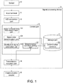
- FIG. 1 is a block diagram showing an example of the main part configuration of the signal processing device 10 in the embodiment.
- the signal processing device 10 is an A/D converter which converts the input analog signal into a digital signal.
- the signal processing device 10 includes an input terminal 11, an A/D conversion part 12, a control part 13, a transmission-reception part (a notification part, a reception part)14 and a storage part 15.
- the input terminal 11 accepts the input of a signal from an external machine.
- the input terminal 11 accepts the input of an analog signal from the sensor 20 in particular.
- the signal processing device 10 may also accept the input of an analog signal from each of a plurality of the sensors 20 by each of a plurality of channels.
- the signal processing device 10 may include a plurality of input terminals 11 corresponding to the plurality of channels.
- the A/D conversion part 12 converts the analog signal output by the sensor 20 into a digital signal cyclically (at a sampling cycle).
- the A/D conversion part 12 directly converts the value of the analog input signal into a digital signal.
- the A/D conversion part 12 converts the value of the analog input signal into a digital signal with the value of the analog input signal as the upper limit value (or the lower limit value) of the input conversion range.
- the A/D conversion part 12 transmits the digital signal to the control part 13.
- the digital signal is transmitted to a signal state determination part 131 in particular.
- the control part 13 includes a CPU (Central Processing Unit), a RAM (Random Access Memory), a ROM (Read Only Memory) and the like, and controls each configuration element according to the information processing.
- the control part 13 includes an upper and lower limit value determination part 130, a signal state determination part 131, a notification signal generation part (a notification part, a display instruction part) 132 and a determination condition setting part 133.
- control part 13 may conduct a filter processing to eliminate the noise of the digital signal.
- the control part 13 may transmits the digital signal to which the filter processing is conducted to the controller 40 via the communication coupler 30.
- the upper and lower limit value determination part 130 determines, in each sampling cycle, whether the value of the digital signal received from the A/D conversion part 12 is the upper limit value or lower limit value of the input conversion range, and notifies, in each sampling cycle for example, the signal state determination part 131 of the determination result.
- the upper and lower limit value determination part 130 may transmit the received digital signal to the signal state determination part 131 only when the value of the received digital signal is the upper limit value or lower limit value of the input conversion range.
- the upper and lower limit value determination part 130 may cause the time series data of the analog input signal to be displayed on an external machine.
- the upper and lower limit value determination part 130 determines whether the value of the digital signal received from the A/D conversion part 12 is above or below a predetermined value.
- the predetermined value is a value set within the input conversion range, and is a value used to determine whether the value of the analog input signal is close to the upper limit value or lower limit value of the input conversion range.
- the predetermined value may be set to two values, one of which is used to determine whether the value of the analog input signal is close to the upper limit value of the input conversion range, and the other of which is used to determine whether the value of the analog input signal is close to the lower limit value of the input conversion range.
- the upper and lower limit value determination part 130 may notify, in accordance with the determination result, the notification signal generation part 132 that the value of the digital signal is above or below the predetermined value (close to the upper limit value or lower limit value of the input conversion range).
- the time series data of the analog input signal can be displayed to the user.
- the display input device 50 may also be a configuration which accepts an instruction of the time series data of the analog input signal from the user and displays the time series data.
- the signal state determination part 131 determines, for the analog input signal, whether an over-range or under-range state lasts longer than a predetermined time.
- the signal state determination part 131 determines whether the receiving of the digital signal indicating the upper limit value or lower limit value of the input conversion range lasts longer than a predetermined time. That is, the signal state determination part 131 determines whether the digital signal in each sampling cycle is continuously determined by the upper and lower limit value determination part 130 to be the upper limit value or lower limit value for longer than a predetermined time (for example, the duration of predetermined integer multiple of the sampling cycle).
- a predetermined time for example, the duration of predetermined integer multiple of the sampling cycle.
- the signal state determination part 131 notifies the notification signal generation part 132 that the analog input signal is in an over-range or under-range state (abnormal state).
- the signal state determination part 131 may also perform the determination with reference to, for example, determination condition 151 stored in the storage part 15 which indicates the predetermined time.
- the signal state determination part 131 determines that the determination result of the upper and lower limit value determination part 130 in each sampling cycle "is the upper limit value or lower limit value” continuously form more than n times. Moreover, in the description below, “n” is “an integer of 1 or more”.
- the signal state determination part 131 determines that an over-range or under-range state occurs. Then, the signal state determination part 131 notifies the notification signal generation part 132 of the determination result. In contrast, when the determination result of the upper and lower limit value determination part 130 is not continuously “the upper limit value or lower limit value" for more than n times, the signal state determination part 131 determines that an over-range or under-range state does not occur.
- the signal state determination part 131 conducts the following processing. That is, the signal state determination part 131 determines whether "the determination result of the upper and lower limit value determination part 130 in each sampling cycle is continuously the upper limit value or lower limit value for more than twice".
- the signal state determination part 131 determines that an over-range or under-range state occurs.
- the signal state determination part 131 determines, when the determination result of the upper and lower limit value determination part 130 in the n-th cycle is "the upper limit value or lower limit value”, and the determination result of the upper and lower limit value determination part 130 in the n+1-th cycle is also "the upper limit value or lower limit value", that an over-range or under-range state occurs.
- the signal state determination part 131 determines that an over-range or under-range state does not occur. That is, even when the determination result of the upper and lower limit value determination part 130 in the n-th cycle is "the upper limit value or lower limit value", if the determination result of the upper and lower limit value determination part 130 in the n+1-th cycle is not "the upper limit value or lower limit value", the signal state determination part 131 determines that an over-range or under-range state does not occur.
- the predetermined time may be set to integer multiple of the sampling period of the analog input signal in the A/D conversion part 12.
- the signal processing device 10 may further include a plurality of channels for the connection to each of the plurality of sensors 20.
- the above-mentioned time series data may be the time series data of one analog input signal input by one channel or the time series data of a plurality of analog input signals input by a plurality of different channels.
- the time series data of one analog input signal input by one channel or the time series data of a plurality of analog input signals input by a plurality of different channels can be displayed to the user. Besides, by displaying the time series data of a plurality of analog input signals input by a plurality of different channels, the user can compare the time series data of the analog input signals input by each channel with each other.
- the notification signal generation part 132 notifies the controller 40 that an over-range or under-range state occurs in the analog input signal.
- the notification signal generation part 132 generates a signal which indicates the state of the analog input signal.
- the notification signal generation part 132 generates, in accordance with an instruction of generating a signal which indicates that the analog input signal of the signal state determination part 131 is in an abnormal state, a signal which indicates that the analog input signal is in an abnormal state.
- the notification signal generation part 132 may generates a signal which indicates that the analog input signal is in a normal state.
- the notification signal generation part 132 transmits the generated signal to the transmission-reception part 14 and instructs a transmission to the controller 40.
- the notification signal generation part 132 may be configured so that once the signal indicating that the analog input signal is in an abnormal state is generated, the signal generation goes on until an input operation of notification cancellation from the user is accepted.
- the notification signal generation part 132 may accept the input operation of notification cancellation of the user from the display input device 50 via the controller 40 and the transmission-reception part 14.
- the notification signal generation part 132 may also perform the following processing.
- the notification signal generation part 132 generates a signal which instructs the controller 40 to display the time series data of the analog input signal through the transmission-reception part 14 and the communication coupler 30.
- the notification signal generation part 132 transmits the generated signal to the transmission-reception part 14 and instructs a transmission to the controller 40.
- the controller 40 may instruct the display input device 50 and so on to display upon receiving the instruction.
- the display of the time series data of the analog input signal may also be conducted when the controller 40 accepts an operation of the user instructing the display via the display input device 50 and so on.
- the determination condition setting part 133 sets the predetermined time according to the user operation. Specifically, the determination condition setting part 133 accepts, from the support device 60 and via the transmission-reception part 14, the user operation on the setting of the predetermined time indicated by the determination condition 151. The determination condition setting part 133 sets the predetermined time indicated by the determination condition 151 based on this operation.
- the controller 40 can be notified of the occurrence of the state.
- the signal processing device 10 when the signal processing device 10 is configured to process a plurality of analog input signals, it may be configured so that the user can set the predetermined time indicated by the determination condition 151 for each analog input signal.
- the signal processing device 10 may be configured as follows. The signal processing device 10 accepts the input data from the user regarding the setting (change) of the predetermined time indicated by the determination condition 151 for each analog input signal, and sets the predetermined time for each analog input signal.
- the transmission-reception part 14 receives the signal from the notification signal generation part 132 and transmits the signal to the communication coupler 30. Besides, the transmission-reception part 14 receives, from the communication coupler 30, the operation input of the user related to the setting of the predetermined time indicated by the determination condition 151, and transmits to the determination condition setting part 133.
- the transmission-reception part 14 transmits the digital signal converted by the A/D conversion part 12 to the communication coupler 30.
- the communication coupler 30 cyclically delivers the signal received from the signal processing device 10 (the transmission-reception part 14) to the controller 40 (control device) in a predetermined delivery cycle.
- the transmission-reception part 14 acquires, from the support device 60 and via the communication coupler 30 and the controller 40, the user operation which sets the predetermined time indicated by the determination condition 151.
- the transmission-reception part 14 transmits the input data to the determination condition setting part 133.
- the storage part 15 is, for example, an auxiliary storage device such as a solid state drive, and stores the above-mentioned determination condition 151 and so on.
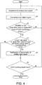
- FIG. 4 is a flowchart showing an example of the flow of abnormality notification determination processing of the analog input signal of the signal processing device 10. An example of the processing flow of the signal processing device 10 is described using FIG. 4 .
- the A/D conversion part 12 cyclically samples (acquires) the analog input signal (SI), and converts the analog input signal into a digital signal (S2).
- the upper and lower limit value determination part 130 determines, in each sampling cycle, whether the value of the converted digital signal is the upper limit value or lower limit value of the input conversion range (S3).
- the processing proceeds to S4 described below.
- the signal state determination part 131 determines, for the converted digital signal, whether the lower limit value or upper limit value of the input conversion range lasts for the predetermined time (S4: signal state determination step). That is, for the number n which satisfies "n times of sampling cycle ⁇ predetermined time", the signal state determination part 131 determines whether the determination result of the upper and lower limit value determination part 130 in each sampling cycle is continuously "the upper limit value or lower limit value" for more than n times.
- the notification signal generation part 132 notifies the controller 40 of the abnormality of the analog signal by transmitting a signal which indicates the state of the analog input signal (S5: notification step).
- S5 notification step
- the processing is ended.
- the processing returns to S1.
- the processing proceeds to S6.
- the processing proceeds to S6.
- FIG. 5 is a flowchart showing an example of the condition setting processing flow of the abnormality notification determination of the analog input signal of the signal processing device 10. An example of the processing flow of the signal processing device 10 is described using FIG. 5 .
- the notification signal generation part 132 instructs the controller 40 to display the time series data of the analog input signal (S11).
- the transmission-reception part 14 receives the input data of the user related to the predetermined time indicated by the determination condition 151 (S12).
- the determination condition setting part 133 changes the predetermined time indicated by the determination condition 151 based on the input data (sets the determination condition) (S13). Then, the processing is ended.
- FIG. 6 is a drawing showing an example of the setting of the predetermined time used for the determination performed by the signal state determination part 131.
- the graph in FIG. 6 represents the time series data of a plurality of analog input signals.
- the display input device 50 may display the graph shown in FIG. 6 as the time series data of the analog input signal.
- channel numbers (ch1-ch4) corresponding to each analog input signal are associated.
- the waveform in the circle of the dotted line in FIG. 6 is the time series data of the analog input signal of ch4. More specifically, the behavior of the value of analog input signal caused by overshoot is shown. As shown in FIG.
- the value of the analog input signal having the time series data of the analog input signal of ch4 exceeds the upper limit value of the input conversion range for 500 microseconds due to overshoot. That is, the analog input signal of ch4 is in an over-range state for 500 microseconds due to overshoot.
- the signal state determination part 131 does not determine the generation of over-range state of the analog input signal caused by overshoot as an abnormal state. Therefore, the controller 40 is not notified of the over-range of the analog input signal caused by overshoot.
- the predetermined time may be set to twice the length of the time in which the analog input signal is in an over-range state (1 millisecond in the example shown in FIG. 7(a) and 7(b) ).
- the signal processing device 10 may also be capable of performing, for example, an A/D conversion processing in which the resolution is 16 Bit or 18 Bit.
- the control block (in particular, the signal state determination part 131, the notification signal generation part 132 and the determination condition setting part 133) of the signal processing device 10 may be realized by a logical circuit (hardware) formed into an integrated circuit (IC chip) or be realized by software.
- the signal processing device 10 includes a computer for executing commands of programs acting as software which fulfills various functions.
- the computer includes, for example, more than one processor and computer readable storage medium which stores the programs. Then, the aim of the present invention is achieved by the processor reading the programs from the storage medium and executing the programs in the computer.
- the processor can be a CPU (Central Processing Unit) for example.
- non-temporary tangible medium such as a ROM (Read Only Memory)
- the storage medium may also be a tape, a disk, a card, a semiconductor memory, a programmable logical circuit and so on.
- a RAM Random Access Memory which develops the program may also be included.
- the program may be supplied to the computer via any transmission medium (a communication network, a broadcast wave or the like) capable of transmitting the program.
- a transmission medium a communication network, a broadcast wave or the like
- one aspect of the present invention can also be realized by the form of a data signal which is embedded in a carrier wave and for which the program is embodied by electronic transmission.
Landscapes
- Engineering & Computer Science (AREA)
- Theoretical Computer Science (AREA)
- Physics & Mathematics (AREA)
- General Physics & Mathematics (AREA)
- Automation & Control Theory (AREA)
- Health & Medical Sciences (AREA)
- Computing Systems (AREA)
- General Health & Medical Sciences (AREA)
- Medical Informatics (AREA)
- Computer Networks & Wireless Communication (AREA)
- Signal Processing (AREA)
- Analogue/Digital Conversion (AREA)
- Arrangements For Transmission Of Measured Signals (AREA)
Abstract
Description
- The present invention relates to a signal processing device and the like, in particular, to a signal processing device which processes a signal from a sensor and delivers the signal to a control device.
- A signal processing device is known which acquires, from a sensor mounted on an industrial machine, such as a measuring device, the physical quantity detected by the sensor, processes the detected signal that is acquired, and delivers the signal to a control device which controls the industrial machine. In such a signal processing device, an analog signal acquired from the sensor is converted into a digital signal by an A/D converter and delivered to the control device.
- For example, in patent literature 1 (Japanese Laid-Open No.
2017-134769 (published on August 3, 2017 - Here, for A/D converters with equal performance, in a case that a division number of an analog input signal is set high, the input conversion range of the analog input signal is limited. Therefore, compared with a case in which the division number of the analog input signal is set low, in the case that the division number of the analog input signal is set high, the value of the analog input signal easily turns into such a state as described below. For example, the value of the analog input signal is in an over-range state in which the value exceeds the input conversion range of the A/D converter, or the value of the analog input signal is in an under-range state in which the value falls below the input conversion range. The detail is described below.
-
FIG. 7(a) and 7(b) are drawings showing an example in which an analog input signal turns into an over-range or under-range state in an A/D converter having a resolution of 16 Bit or 18 Bit.FIG. 7(a) shows an example of the state of the analog input signal when a division number of the analog input signal is set to 30000 under full-scale upper and lower limit values (+10 V, -10 V). Besides,FIG. 7(b) shows an example of the state of the analog input signal when the division number of the analog input signal is set to 64000 under the full-scale upper and lower limit values (+10 V, -10 V). As shown inFIG. 7(a) , when the division number is set to as low as 30000, the input conversion range is set to 105% and -5% of the full-scale upper and lower limit values. That is, the upper limit value of the input conversion range is +11 V, and the lower limit value is -11 V. Therefore, as long as the value of the analog input signal does not reach +11 V or not fall below -11 V, the analog input signal does not turn to an over-range or under-range state. In contrast, as shown inFIG. 7(b) , when the division number is set to as high as 64000, the input conversion range is necessarily limited to 101% and -1% of the full-scale upper and lower limit values. That is, the upper limit value of the input conversion range is +10.2 V, and the lower limit value is -10.2 V. Therefore, compared with the case that the division number is set to as low as 30000, the frequency at which the analog input signal turns into an over-range or under-range state increases. Besides, inFIG. 7(a) and FIG. 7(b) , the time series data of the analog input signal when overshoot occurs is shown. As shown inFIG. 7(a) , when the upper limit value of the input conversion range is +11 V, the value of the analog input signal does not exceed the upper limit value. On the other hand, as shown inFIG. 7(b) , when the upper limit value of the input conversion range is +10.2 V, the value of the analog input signal exceeds the upper limit value. That is, by setting a high division number, the input conversion range becomes narrow; as a result, the analog input signal easily turns over-range or under-range. - For example, when the analog input signal turns into an over-range or under-range state, in a configuration in which a notification showing the abnormality of the analog signal is given, such problems as described below come up. That is, when the division number is set high, the notification showing the abnormality of the analog signal is frequently given. For example, the over-range or under-range state of the analog input signal caused by overshoot or undershoot is not necessarily a case in which an abnormal state occurs. However, if the notification showing the abnormality of the analog signal is frequently given even in such a case, problems such a decrease in the operation rate are caused.
- Such related art as shown in the above-mentioned
patent literature 1 is a technology of eliminating the noise in the signal, other than a technology intending to suppress an unnecessary "notification that shows an abnormality". One aspect of the present invention aims to realize a signal processing device which can suppress an unnecessary notification in the notification showing an abnormality of the analog signal. - In order to solve the problems, the signal processing device of one aspect of the present invention is a signal processing device that processes an analog input signal from a sensor and delivers the signal to a control device, and includes: a signal state determination part, which determines, for the analog input signal, whether an over-range or under-range state lasts longer than a predetermined time; and a notification part, which notifies the control device that an over-range or under-range state occurs when the signal state determination part determines that the state lasts longer than the predetermined time.
- Besides, a control method of the signal processing device of one aspect of the present invention is a control method of a signal processing device which processes an analog input signal from a sensor and delivers the signal to a control device, and includes: a signal state determination step, which determines, for the analog input signal, whether an over-range or under-range state lasts longer than a predetermined time; and a notification step, which notifies the control device that the over-range or under-range state occurs when it is determined in the signal state determination step that the state lasts longer than the predetermined time.
- According to the above configuration, even if the analog input signal turns into an over-range or under-range state (abnormal state), when the state does not last for a predetermined time, the notification is not given which shows the over-range or under-range state of the analog input signal. For example, when the analog input signal turns into an abnormal state because of overshoot or undershoot, the cause of the state is not the failure in the sensor and so on. Therefore, the notification to the effect that the analog input signal is in an abnormal state is unnecessary. Besides, the duration of the abnormal state of the analog input signal caused by overshoot or undershoot is limited. Therefore, by appropriately setting the predetermined time, the notification of abnormal state caused by overshoot or undershoot can be suppressed.
- The signal processing device of one aspect of the present invention may also include a reception part which acquires a user operation that sets the predetermined time; and a determination condition setting part which sets the predetermined time in accordance with the user operation.
- According to the above configuration, for the analog input signal, when the over-range or under-range state lasts longer than the predetermined time desired by the user, the control device can be notified that the state occurs.
- The signal processing device of one aspect of the present invention may also include a display instruction part which causes time series data of the analog input signal to be displayed on an external machine. According to the above-mentioned configuration, the time series data of the analog input signal can be shown to the user.
- The signal processing device of one aspect of the present invention may further include a plurality of channels for connection to each of a plurality of the sensors, and the time series data may be the time series data of one of the analog input signals input by one of the channels, or be the time series data of a plurality of the analog input signals input by a plurality of different channels.
- According to the above-mentioned configuration, the time series data of one analog input signal input by one channel, or the time series data of a plurality of analog input signals input by a plurality of different channels can be shown to the user. Besides, by displaying the time series data of a plurality of analog input signals input by a plurality of different channels, the user can compare the time series data of the analog input signals input by each channel.
- In the signal processing device of one aspect of the present invention, the predetermined time may be the integer multiple of a sampling period of the analog input signals by the signal processing device.
- According to the above-mentioned configuration, for the analog input signals sampled continuously by the signal processing device for predetermined times, when the over-range or under-range state lasts, the occurrence of the state can be notified.
- In the signal processing device of one aspect of the present invention, the control device may be a master device in a master-slave control system, and the signal processing device may be a slave device connected to the master device via a network.
- According to the above-mentioned configuration, the signal processing device can be applied in a master-slave control system.
- According to one aspect of the present invention, unnecessary notification can be suppressed in the notification showing abnormality of the analog signal.
-
-
FIG. 1 is a block diagram showing an example of a main part configuration of a signal processing device in an embodiment of the present invention. - (a) of
FIG. 2 and (b) ofFIG.2 are drawings showing an example of a processing performed to an analog input signal by a signal processing device of an embodiment of the present invention. -
FIG. 3 is a drawing showing an overview of a control system of an embodiment of the present invention. -
FIG. 4 is a flowchart showing an example of a processing flow of a signal processing device in an embodiment of the present invention. -
FIG. 5 is a flowchart showing another example of a processing flow of a signal processing device in an embodiment of the present invention. -
FIG. 6 is a drawing showing an example of setting a predetermined time used for the determination performed by a signal state determination part of an embodiment of the present invention. -
FIG. 7(a) and 7(b) are drawings showing an example in which an analog input signal turns into an over-range or under-range state. - Next, an embodiment of one aspect of the present invention (also referred to as "the embodiment" hereinafter) is described based on the drawings.
- A
signal processing device 10 determines, for an analog input signal, whether an over-range or under-range state lasts longer than a predetermined time. When the state lasts longer than a predetermined time, thesignal processing device 10 notifies a controller (control device) 40 that an over-range or under-range state occurs in the analog input signal. - (a) of
FIG. 2 and (b) ofFIG.2 are drawings showing an example of a processing performed to the analog input signal by thesignal processing device 10 of the embodiment. Specifically, (a) ofFIG. 2 is a drawing showing an example of a processing in which thesignal processing device 10 converts the analog input signal into a digital signal. In (a) ofFIG. 2 , the value of the analog input signal (analog input signal) is represented by a solid line, and the value of the digital signal (converted value) is represented a dotted line. As shown in (a) ofFIG. 2 , when the value of the analog input signal is within the input conversion range, thesignal processing device 10 directly converts the value of the analog input signal into a digital signal. On the other hand, when the value of the analog input signal is out of the input conversion range, thesignal processing device 10 converts the value of the analog input signal into a digital signal with the value of the analog input signal as the upper limit value (or the lower limit value) of the input conversion range. - (b) of
FIG.2 is a drawing showing an example of the generation of the signal sent by thesignal processing device 10 to the controller 40 (the signal which notifies thecontroller 40 that an over-range or under-range state occurs). The signal indicates the state of the analog input signal by values. As shown in (b) ofFIG. 2 , the signal indicating the value of 1 indicates that analog input signal is in an over-range or under-range state (abnormal state). Besides, the signal indicating the value of 0 indicates that the analog input signal is in a normal state. In the example shown in (b) ofFIG. 2 , when the over-range or under-range state lasts longer than the predetermined time (100 ms in the example shown in (b) ofFIG. 2 ), thesignal processing device 10 generates the signal which indicates the value of 1. Upon receiving the signal which indicates the value of 1 (the signal which indicates that the analog input signal is in an abnormal state), thecontroller 40 causes the images showing that the analog input signal is in an abnormal state to be displayed on adisplay input device 50. Besides, thesignal processing device 10 may be configured to accept an input operation of the user which cancels the normality notification through an external machine (such as asupport device 60 described below), and restore the value of the signal to 0. - According to the above-mentioned configuration, even if the analog input signal turns into an over-range or under-range state, when the state does not last longer than 100 ms, the notification that the analog input signal is in an abnormal state is not performed. For example, when the analog input signal is in an over-range or under-range state (abnormal state) because of overshoot or undershoot, the cause of the state is not the failure in the sensor and so on. Therefore, the notification to the effect that the analog input signal is in an abnormal state is unnecessary. Besides, the duration of the abnormal state of the analog input signal caused by overshoot or undershoot is limited. Therefore, by appropriately setting the predetermined time, the notification of abnormal state of the analog input signal caused by overshoot or undershoot can be suppressed.
- Besides, the
signal processing device 10 may be configured to receive a plurality of analog input signals from a plurality of sensors, and may perform the abnormality notification processing to each analog input signal. -
FIG. 3 is a drawing showing an overview of acontrol system 1 of the embodiment. As shown inFIG. 3 , thecontrol system 1 includes a plurality ofsensors 20, asignal processing device 10, acommunication coupler 30, acontroller 40, adisplay input device 50 and asupport device 60. - For example, the
controller 40 is a master device, and thesignal processing device 10 is a slave device connected to the master device via a high-order bus, namely a high-order communication network. In other words, thecontrol system 1 may be a master-slave control system which includes thecontroller 40 serving as the master device, and more than onesignal processing devices 10 connected to the master device via the network and serving as slave devices. While thecontroller 40 is called a "master device" in the sense of management of data transmission via the high-order communication network, thesignal processing device 10 is called a "slave device". - As shown in
FIG. 3 , thesignal processing device 10 is a relay device which relays data between a high-order network including thecontroller 40 and the like and the sensor 2. In the embodiment, thesignal processing device 10 is an A/D converter which converts the analog signal to a digital signal. - The
communication coupler 30 is a relay device which relays the communication between the high-order network and thesignal processing device 10. Thecommunication coupler 30 relays the communication between the machine included in the high-order network and thesignal processing device 10. - The
sensor 20 detects the physical quantity (state value) of a control target (not shown), and outputs the signal corresponding to the detected physical quantity (for example, an analog signal) to thesignal processing device 10. The state value of the control target detected by thesensor 20 may be any physical quantity such as weight, pressure and so on. As shown inFIG. 3 , thesensor 20 is a device connected to thesignal processing device 10 for communication and becomes the control target of thecontroller 40. - The
controller 40 is a control device which integrally controls thewhole control system 1, for example, a PLC (Programmable Logic Controller). Thecontroller 40 acts as the master device of thesignal processing device 10 in thecontrol system 1. As shown inFIG. 3 , thesupport device 60, thedisplay input device 50 and so on may be connected to thecontroller 40 via a connection cable and the like. - The
support device 60 is a device connected to thecontrol system 1 to be used for various settings in thecontrol system 1 such as the operation setting of thesensor 20 and thesignal processing device 10. Thesupport device 60 can be connected to thecontrol system 1 through thecontroller 40. Thesupport device 60 may be an information processing device such as a personal computer or a portable information device such as a notebook computer. Moreover, thesupport device 60 may also connected to thesignal processing device 10 via thecommunication coupler 30 and perform various settings. - The
display input device 50 is, for example, a touch-panel type display input device. The user of thecontrol system 1 can operate thecontroller 40 via thedisplay input device 50, or confirm the operation state of thecontrol system 1 with thedisplay input device 50. -
FIG. 1 is a block diagram showing an example of the main part configuration of thesignal processing device 10 in the embodiment. As described above, thesignal processing device 10 is an A/D converter which converts the input analog signal into a digital signal. As shown inFIG. 1 , thesignal processing device 10 includes aninput terminal 11, an A/D conversion part 12, acontrol part 13, a transmission-reception part (a notification part, a reception part)14 and astorage part 15. - The
input terminal 11 accepts the input of a signal from an external machine. In the embodiment, theinput terminal 11 accepts the input of an analog signal from thesensor 20 in particular. Besides, thesignal processing device 10 may also accept the input of an analog signal from each of a plurality of thesensors 20 by each of a plurality of channels. In this configuration, thesignal processing device 10 may include a plurality ofinput terminals 11 corresponding to the plurality of channels. - The A/
D conversion part 12 converts the analog signal output by thesensor 20 into a digital signal cyclically (at a sampling cycle). - Specifically, when the value of the analog signal (analog input signal) output by the
sensor 20 is within the input conversion range, the A/D conversion part 12 directly converts the value of the analog input signal into a digital signal. On the other hand, when the value of the analog input signal is out of the input conversion range, the A/D conversion part 12 converts the value of the analog input signal into a digital signal with the value of the analog input signal as the upper limit value (or the lower limit value) of the input conversion range. - The A/
D conversion part 12 transmits the digital signal to thecontrol part 13. In the embodiment, the digital signal is transmitted to a signalstate determination part 131 in particular. - The
control part 13 includes a CPU (Central Processing Unit), a RAM (Random Access Memory), a ROM (Read Only Memory) and the like, and controls each configuration element according to the information processing. Thecontrol part 13 includes an upper and lower limitvalue determination part 130, a signalstate determination part 131, a notification signal generation part (a notification part, a display instruction part) 132 and a determinationcondition setting part 133. - Besides, the
control part 13 may conduct a filter processing to eliminate the noise of the digital signal. Thecontrol part 13 may transmits the digital signal to which the filter processing is conducted to thecontroller 40 via thecommunication coupler 30. - The upper and lower limit
value determination part 130 determines, in each sampling cycle, whether the value of the digital signal received from the A/D conversion part 12 is the upper limit value or lower limit value of the input conversion range, and notifies, in each sampling cycle for example, the signalstate determination part 131 of the determination result. The upper and lower limitvalue determination part 130 may transmit the received digital signal to the signalstate determination part 131 only when the value of the received digital signal is the upper limit value or lower limit value of the input conversion range. - Besides, the upper and lower limit
value determination part 130 may cause the time series data of the analog input signal to be displayed on an external machine. - For example, the upper and lower limit
value determination part 130 determines whether the value of the digital signal received from the A/D conversion part 12 is above or below a predetermined value. Here, the predetermined value is a value set within the input conversion range, and is a value used to determine whether the value of the analog input signal is close to the upper limit value or lower limit value of the input conversion range. For example, the predetermined value may be set to two values, one of which is used to determine whether the value of the analog input signal is close to the upper limit value of the input conversion range, and the other of which is used to determine whether the value of the analog input signal is close to the lower limit value of the input conversion range. The upper and lower limitvalue determination part 130 may notify, in accordance with the determination result, the notificationsignal generation part 132 that the value of the digital signal is above or below the predetermined value (close to the upper limit value or lower limit value of the input conversion range). - According to the above-mentioned configuration, the time series data of the analog input signal can be displayed to the user. Moreover, the
display input device 50 may also be a configuration which accepts an instruction of the time series data of the analog input signal from the user and displays the time series data. - The signal
state determination part 131 determines, for the analog input signal, whether an over-range or under-range state lasts longer than a predetermined time. - Specifically, the signal
state determination part 131 determines whether the receiving of the digital signal indicating the upper limit value or lower limit value of the input conversion range lasts longer than a predetermined time. That is, the signalstate determination part 131 determines whether the digital signal in each sampling cycle is continuously determined by the upper and lower limitvalue determination part 130 to be the upper limit value or lower limit value for longer than a predetermined time (for example, the duration of predetermined integer multiple of the sampling cycle). When the receiving of the digital signal indicating the upper limit value or lower limit value of the input conversion range lasts longer than the predetermined time, the signalstate determination part 131 notifies the notificationsignal generation part 132 that the analog input signal is in an over-range or under-range state (abnormal state). The signalstate determination part 131 may also perform the determination with reference to, for example,determination condition 151 stored in thestorage part 15 which indicates the predetermined time. - When "n times of the sampling cycle ≥ the predetermined time", the signal
state determination part 131 determines that the determination result of the upper and lower limitvalue determination part 130 in each sampling cycle "is the upper limit value or lower limit value" continuously form more than n times. Moreover, in the description below, "n" is "an integer of 1 or more". - When the determination result of the upper and lower limit
value determination part 130 in each sampling cycle is continuously "the upper limit value or lower limit value" for more than n times, the signalstate determination part 131 determines that an over-range or under-range state occurs. Then, the signalstate determination part 131 notifies the notificationsignal generation part 132 of the determination result. In contrast, when the determination result of the upper and lower limitvalue determination part 130 is not continuously "the upper limit value or lower limit value" for more than n times, the signalstate determination part 131 determines that an over-range or under-range state does not occur. - For example, in a case of "sampling cycle = 50 ms", and "twice of sampling cycle=100 ms ≥ predetermined time > 50 ms = one time of sampling cycle", the signal
state determination part 131 conducts the following processing. That is, the signalstate determination part 131 determines whether "the determination result of the upper and lower limitvalue determination part 130 in each sampling cycle is continuously the upper limit value or lower limit value for more than twice". - When it is determined that "the determination result of the upper and lower limit
value determination part 130 in each sampling cycle is continuously 'the upper limit value or lower limit value' for more than twice", the signalstate determination part 131 determines that an over-range or under-range state occurs. The signalstate determination part 131 determines, when the determination result of the upper and lower limitvalue determination part 130 in the n-th cycle is "the upper limit value or lower limit value", and the determination result of the upper and lower limitvalue determination part 130 in the n+1-th cycle is also "the upper limit value or lower limit value", that an over-range or under-range state occurs. - In contrast, when it is determined that "even if one of the determination result of the upper and lower limit
value determination part 130 in each sampling cycle is 'the upper limit value or lower limit value', the determination result of the upper and lower limitvalue determination part 130 is not continuously 'the upper limit value or lower limit value"', the signalstate determination part 131 determines that an over-range or under-range state does not occur. That is, even when the determination result of the upper and lower limitvalue determination part 130 in the n-th cycle is "the upper limit value or lower limit value", if the determination result of the upper and lower limitvalue determination part 130 in the n+1-th cycle is not "the upper limit value or lower limit value", the signalstate determination part 131 determines that an over-range or under-range state does not occur. - Besides, the predetermined time may be set to integer multiple of the sampling period of the analog input signal in the A/
D conversion part 12. - According to the above-mentioned configuration, when an over-range or under-range state lasts for analog input signals continuously sampled by the A/
D conversion part 12 for predetermined times, it can be determined that the state occurs. - Besides, the
signal processing device 10 may further include a plurality of channels for the connection to each of the plurality ofsensors 20. The above-mentioned time series data may be the time series data of one analog input signal input by one channel or the time series data of a plurality of analog input signals input by a plurality of different channels. - According to the above-mentioned configuration, the time series data of one analog input signal input by one channel or the time series data of a plurality of analog input signals input by a plurality of different channels can be displayed to the user. Besides, by displaying the time series data of a plurality of analog input signals input by a plurality of different channels, the user can compare the time series data of the analog input signals input by each channel with each other.
- In accordance with the determination result of the signal
state determination part 131, the notificationsignal generation part 132 notifies thecontroller 40 that an over-range or under-range state occurs in the analog input signal. - Specifically, the notification
signal generation part 132 generates a signal which indicates the state of the analog input signal. The notificationsignal generation part 132 generates, in accordance with an instruction of generating a signal which indicates that the analog input signal of the signalstate determination part 131 is in an abnormal state, a signal which indicates that the analog input signal is in an abnormal state. Moreover, when such an instruction is not received from the signalstate determination part 131, the notificationsignal generation part 132 may generates a signal which indicates that the analog input signal is in a normal state. Detailed example of the signal which indicates the state of the analog input signal is described in the above-mentioned ''§1 Application example", therefore repeated description is omitted here. The notificationsignal generation part 132 transmits the generated signal to the transmission-reception part 14 and instructs a transmission to thecontroller 40. - Besides, the notification
signal generation part 132 may be configured so that once the signal indicating that the analog input signal is in an abnormal state is generated, the signal generation goes on until an input operation of notification cancellation from the user is accepted. For example, the notificationsignal generation part 132 may accept the input operation of notification cancellation of the user from thedisplay input device 50 via thecontroller 40 and the transmission-reception part 14. - Besides, when the upper and lower limit
value determination part 130 determines that the value of the analog input signal is close to the upper limit value or lower limit value of the input conversion range, the notificationsignal generation part 132 may also perform the following processing. The notificationsignal generation part 132 generates a signal which instructs thecontroller 40 to display the time series data of the analog input signal through the transmission-reception part 14 and thecommunication coupler 30. - The notification
signal generation part 132 transmits the generated signal to the transmission-reception part 14 and instructs a transmission to thecontroller 40. Thecontroller 40 may instruct thedisplay input device 50 and so on to display upon receiving the instruction. - Besides, the display of the time series data of the analog input signal may also be conducted when the
controller 40 accepts an operation of the user instructing the display via thedisplay input device 50 and so on. - The determination
condition setting part 133 sets the predetermined time according to the user operation. Specifically, the determinationcondition setting part 133 accepts, from thesupport device 60 and via the transmission-reception part 14, the user operation on the setting of the predetermined time indicated by thedetermination condition 151. The determinationcondition setting part 133 sets the predetermined time indicated by thedetermination condition 151 based on this operation. - According to the above-mentioned configuration, for the analog input signal, when an over-range or under-range state lasts longer than the predetermined time desired by the user, the
controller 40 can be notified of the occurrence of the state. Besides, when thesignal processing device 10 is configured to process a plurality of analog input signals, it may be configured so that the user can set the predetermined time indicated by thedetermination condition 151 for each analog input signal. For example, when thedisplay input device 50 is configured to display the time series data (for example, waveform data) of a plurality of analog input signals, thesignal processing device 10 may be configured as follows. Thesignal processing device 10 accepts the input data from the user regarding the setting (change) of the predetermined time indicated by thedetermination condition 151 for each analog input signal, and sets the predetermined time for each analog input signal. - The transmission-
reception part 14 receives the signal from the notificationsignal generation part 132 and transmits the signal to thecommunication coupler 30. Besides, the transmission-reception part 14 receives, from thecommunication coupler 30, the operation input of the user related to the setting of the predetermined time indicated by thedetermination condition 151, and transmits to the determinationcondition setting part 133. - Besides, the transmission-
reception part 14 transmits the digital signal converted by the A/D conversion part 12 to thecommunication coupler 30. Thecommunication coupler 30 cyclically delivers the signal received from the signal processing device 10 (the transmission-reception part 14) to the controller 40 (control device) in a predetermined delivery cycle. - Besides, the transmission-
reception part 14 acquires, from thesupport device 60 and via thecommunication coupler 30 and thecontroller 40, the user operation which sets the predetermined time indicated by thedetermination condition 151. The transmission-reception part 14 transmits the input data to the determinationcondition setting part 133. - The
storage part 15 is, for example, an auxiliary storage device such as a solid state drive, and stores the above-mentioneddetermination condition 151 and so on. -
FIG. 4 is a flowchart showing an example of the flow of abnormality notification determination processing of the analog input signal of thesignal processing device 10. An example of the processing flow of thesignal processing device 10 is described usingFIG. 4 . The A/D conversion part 12 cyclically samples (acquires) the analog input signal (SI), and converts the analog input signal into a digital signal (S2). Next, the upper and lower limitvalue determination part 130 determines, in each sampling cycle, whether the value of the converted digital signal is the upper limit value or lower limit value of the input conversion range (S3). When the value of the converted digital signal is the upper limit value or lower limit value of the input conversion range ("YES" in S3), the processing proceeds to S4 described below. The signalstate determination part 131 determines, for the converted digital signal, whether the lower limit value or upper limit value of the input conversion range lasts for the predetermined time (S4: signal state determination step). That is, for the number n which satisfies "n times of sampling cycle ≥ predetermined time", the signalstate determination part 131 determines whether the determination result of the upper and lower limitvalue determination part 130 in each sampling cycle is continuously "the upper limit value or lower limit value" for more than n times. When the value of the digital signal lasts for the predetermined time in the form of the lower limit value or the upper limit value ("YES" in S4), the notificationsignal generation part 132 notifies thecontroller 40 of the abnormality of the analog signal by transmitting a signal which indicates the state of the analog input signal (S5: notification step). Next, when the input of the analog signal is ended ("YES" in S6), the processing is ended. Moreover, when the input of the analog signal is not ended ("NO" in S6), the processing returns to S1. Besides, when the lower limit value or upper limit value does not last for the predetermined time ("NO" in S4), the processing proceeds to S6. Besides, when the value of the converted digital signal is not the upper limit value or lower limit value of the input conversion range ("NO" in S3), the processing also proceeds to S6. -
FIG. 5 is a flowchart showing an example of the condition setting processing flow of the abnormality notification determination of the analog input signal of thesignal processing device 10. An example of the processing flow of thesignal processing device 10 is described usingFIG. 5 . The notificationsignal generation part 132 instructs thecontroller 40 to display the time series data of the analog input signal (S11). Next, the transmission-reception part 14 receives the input data of the user related to the predetermined time indicated by the determination condition 151 (S12). Next, the determinationcondition setting part 133 changes the predetermined time indicated by thedetermination condition 151 based on the input data (sets the determination condition) (S13). Then, the processing is ended. -
FIG. 6 is a drawing showing an example of the setting of the predetermined time used for the determination performed by the signalstate determination part 131. The graph inFIG. 6 represents the time series data of a plurality of analog input signals. For example, thedisplay input device 50 may display the graph shown inFIG. 6 as the time series data of the analog input signal. In the graph shown inFIG. 6 , channel numbers (ch1-ch4) corresponding to each analog input signal are associated. The waveform in the circle of the dotted line inFIG. 6 is the time series data of the analog input signal of ch4. More specifically, the behavior of the value of analog input signal caused by overshoot is shown. As shown inFIG. 6 , the value of the analog input signal having the time series data of the analog input signal of ch4 exceeds the upper limit value of the input conversion range for 500 microseconds due to overshoot. That is, the analog input signal of ch4 is in an over-range state for 500 microseconds due to overshoot. - For example, when the predetermined time is set longer than 500 microseconds, the signal
state determination part 131 does not determine the generation of over-range state of the analog input signal caused by overshoot as an abnormal state. Therefore, thecontroller 40 is not notified of the over-range of the analog input signal caused by overshoot. For example, taking the margin into consideration, the predetermined time may be set to twice the length of the time in which the analog input signal is in an over-range state (1 millisecond in the example shown inFIG. 7(a) and 7(b) ). - The
signal processing device 10 may also be capable of performing, for example, an A/D conversion processing in which the resolution is 16 Bit or 18 Bit. - The control block (in particular, the signal
state determination part 131, the notificationsignal generation part 132 and the determination condition setting part 133) of thesignal processing device 10 may be realized by a logical circuit (hardware) formed into an integrated circuit (IC chip) or be realized by software. - In the case of the latter, the
signal processing device 10 includes a computer for executing commands of programs acting as software which fulfills various functions. The computer includes, for example, more than one processor and computer readable storage medium which stores the programs. Then, the aim of the present invention is achieved by the processor reading the programs from the storage medium and executing the programs in the computer. The processor can be a CPU (Central Processing Unit) for example. Besides "non-temporary tangible medium" such as a ROM (Read Only Memory), the storage medium may also be a tape, a disk, a card, a semiconductor memory, a programmable logical circuit and so on. In addition, a RAM (Random Access Memory) which develops the program may also be included. Besides, the program may be supplied to the computer via any transmission medium (a communication network, a broadcast wave or the like) capable of transmitting the program. Moreover, one aspect of the present invention can also be realized by the form of a data signal which is embedded in a carrier wave and for which the program is embodied by electronic transmission. -
- 1
- control system (master-slave control system)
- 10
- signal processing device
- 14
- transmission-reception part (notification part, reception part)
- 20
- sensor
- 40
- controller (control device)
- 130
- upper and lower limit value determination part (display instruction part)
- 131
- signal state determination part
- 132
- notification signal generation part (notification part, display instruction part)
- 133
- determination condition setting part
- S3
- signal state determination step
- S4
- notification step
Claims (7)
- A signal processing device (10), characterized in that the signal processing device (10) processes an analog input signal from a sensor (20) and delivers the signal to a control device (40), the signal processing device (10) comprises:a signal state determination part (131), which determines, for the analog input signal, whether an over-range or under-range state lasts longer than a predetermined time; anda notification part (132), which notifies the control device (40) that the over-range or under-range state occurs when the signal state determination part (131) determines that the state lasts longer than the predetermined time.
- The signal processing device (10) according to claim 1, comprising:a reception part (14), which acquires a user operation that sets the predetermined time; anda determination condition setting part (133), which sets the predetermined time in accordance with the user operation.
- The signal processing device (10) according to claim 1 or 2, comprising:a display instruction part, which causes time series data of the analog input signal to be displayed on an external machine.
- The signal processing device (10) according to claim 3, further comprising a plurality of channels (ch1, ch2, ch3, ch4) for connection to each of a plurality of the sensors (20),
wherein the time series data is the time series data of one of the analog input signals input by one of the channels (ch1, ch2, ch3, ch4), or the time series data of a plurality of the analog input signals input by a plurality of different channels. - The signal processing device (10) according to any one of claims 1 to 4, wherein the predetermined time is the integer multiple of a sampling period of the analog input signals in the signal processing device (10).
- The signal processing device (10) according to any one of claims 1 to 5, wherein the control device (40) is a master device in a master-slave control system (1), and
the signal processing device (10) is a slave device connected to the master device via a network. - A control method of a signal processing device (10), characterized in that the signal processing device (10) processes an analog input signal from a sensor (20) and delivers the signal to a control device (40), the control method comprises:a signal state determination step, which determines, for the analog input signal, whether an over-range or under-range state lasts longer than a predetermined time; anda notification step, which notifies the control device (40) that the over-range or under-range state occurs when it is determined in the signal state determination step that the state lasts longer than the predetermined time.
Applications Claiming Priority (1)
| Application Number | Priority Date | Filing Date | Title |
|---|---|---|---|
| JP2018001761A JP6984422B2 (en) | 2018-01-10 | 2018-01-10 | Signal processing device and control method of signal processing device |
Publications (2)
| Publication Number | Publication Date |
|---|---|
| EP3511786A1 true EP3511786A1 (en) | 2019-07-17 |
| EP3511786B1 EP3511786B1 (en) | 2021-01-13 |
Family
ID=63921504
Family Applications (1)
| Application Number | Title | Priority Date | Filing Date |
|---|---|---|---|
| EP18200199.0A Not-in-force EP3511786B1 (en) | 2018-01-10 | 2018-10-12 | Signal processing device and control method of signal processing device |
Country Status (4)
| Country | Link |
|---|---|
| US (1) | US20190212715A1 (en) |
| EP (1) | EP3511786B1 (en) |
| JP (1) | JP6984422B2 (en) |
| CN (1) | CN110018650B (en) |
Families Citing this family (4)
| Publication number | Priority date | Publication date | Assignee | Title |
|---|---|---|---|---|
| US12580601B2 (en) | 2022-06-28 | 2026-03-17 | Silicon Laboratories Inc. | Control of configurable receiver front end module based at least in part on signal metric information |
| US12431929B2 (en) | 2022-06-28 | 2025-09-30 | Silicon Laboratories Inc. | Configurable receiver front end module having configurable detection capabilities |
| US12593222B2 (en) | 2022-06-28 | 2026-03-31 | Silicon Laboratories Inc. | Central entity update of configurable receiver front end module between static modes |
| US20230421193A1 (en) * | 2022-06-28 | 2023-12-28 | Silicon Laboratories Inc. | Reconfiguration of configurable receiver front end module between plurality of modes |
Citations (3)
| Publication number | Priority date | Publication date | Assignee | Title |
|---|---|---|---|---|
| US4596977A (en) * | 1984-12-03 | 1986-06-24 | Honeywell Inc. | Dual slope analog to digital converter with out-of-range reset |
| US4908623A (en) * | 1988-08-08 | 1990-03-13 | Honeywell Inc. | Apparatus and method for range control and supply voltage compensation in a dual slope analog to digital converter |
| JP2017134769A (en) | 2016-01-29 | 2017-08-03 | オムロン株式会社 | Signal processing apparatus, signal processing method, information processing program, and recording medium |
Family Cites Families (13)
| Publication number | Priority date | Publication date | Assignee | Title |
|---|---|---|---|---|
| US5296856A (en) * | 1993-03-04 | 1994-03-22 | Mantong Frank L | Window tracking ADC |
| US5886622A (en) * | 1994-06-24 | 1999-03-23 | Jon Snyder, Inc. | Alarm system with sensor signal evaluator |
| US6741169B2 (en) * | 2001-07-06 | 2004-05-25 | Trw Inc. | Tire tread integrity monitoring system and method |
| US7049824B2 (en) * | 2003-03-27 | 2006-05-23 | International Business Machines Corporation | Differential particulate detection system for electronic devices |
| US20070257642A1 (en) * | 2003-06-19 | 2007-11-08 | Sean Xiao | Battery cell monitoring and balancing circuit |
| JP5644586B2 (en) * | 2011-02-28 | 2014-12-24 | 株式会社ノーリツ | Remote control and remote control system |
| CN202102074U (en) * | 2011-06-03 | 2012-01-04 | 北京恒源利通电力技术有限公司 | Ekl fault indicator |
| US10289108B2 (en) * | 2012-03-15 | 2019-05-14 | General Electric Company | Methods and apparatus for monitoring operation of a system asset |
| CN102801422B (en) * | 2012-08-17 | 2016-06-15 | 中国科学院微电子研究所 | Successive Approximation Analog-to-Digital Converter |
| CA2836431C (en) * | 2013-12-16 | 2018-02-20 | Blue Ocean Laboratories, Inc. | A sleep system for obtaining sleep information |
| MX2023002575A (en) * | 2014-06-05 | 2023-03-13 | Deka Products Lp | System for calculating a change in fluid volume in a pumping chamber. |
| US20160217674A1 (en) * | 2015-01-26 | 2016-07-28 | Trane International Inc. | Remote monitoring of an hvac system for fault detection and diagnostics |
| JP6598592B2 (en) * | 2015-08-28 | 2019-10-30 | ルネサスエレクトロニクス株式会社 | Semiconductor integrated circuit and electronic control unit |
-
2018
- 2018-01-10 JP JP2018001761A patent/JP6984422B2/en not_active Expired - Fee Related
- 2018-10-11 CN CN201811184801.2A patent/CN110018650B/en not_active Expired - Fee Related
- 2018-10-12 EP EP18200199.0A patent/EP3511786B1/en not_active Not-in-force
- 2018-10-17 US US16/162,404 patent/US20190212715A1/en not_active Abandoned
Patent Citations (3)
| Publication number | Priority date | Publication date | Assignee | Title |
|---|---|---|---|---|
| US4596977A (en) * | 1984-12-03 | 1986-06-24 | Honeywell Inc. | Dual slope analog to digital converter with out-of-range reset |
| US4908623A (en) * | 1988-08-08 | 1990-03-13 | Honeywell Inc. | Apparatus and method for range control and supply voltage compensation in a dual slope analog to digital converter |
| JP2017134769A (en) | 2016-01-29 | 2017-08-03 | オムロン株式会社 | Signal processing apparatus, signal processing method, information processing program, and recording medium |
Also Published As
| Publication number | Publication date |
|---|---|
| CN110018650A (en) | 2019-07-16 |
| JP6984422B2 (en) | 2021-12-22 |
| JP2019121262A (en) | 2019-07-22 |
| CN110018650B (en) | 2022-08-30 |
| EP3511786B1 (en) | 2021-01-13 |
| US20190212715A1 (en) | 2019-07-11 |
Similar Documents
| Publication | Publication Date | Title |
|---|---|---|
| EP3511786B1 (en) | Signal processing device and control method of signal processing device | |
| EP2658129B1 (en) | Synchronization of multiple signal converters | |
| US8176351B2 (en) | Sampling mechanism for data acquisition counters | |
| US9970974B2 (en) | On-line status diagnosis device and on-line status diagnosis method for electric power utilities | |
| EP3200346B1 (en) | Signal processing device, control method thereof, control procedure and recording medium | |
| EP1875611A1 (en) | Selectable real time sample triggering for a plurality of inputs of an analog-to-digital converter | |
| KR20140072373A (en) | Apparatus of Digital-data Transmission for Controling Multi-channel SQUID System | |
| EP3222976A1 (en) | Field device and detector | |
| US10986556B2 (en) | Circuit for monitoring a data processing system | |
| US7209868B2 (en) | Signal monitoring system and method | |
| US20200116785A1 (en) | Safety circuit and method for testing a safety circuit in an automation system | |
| EP3968302B1 (en) | Signal measurement unit | |
| WO2019155985A1 (en) | Recording device and recording method | |
| KR101963524B1 (en) | Data acquisition system | |
| CN108918937B (en) | Universal oscillographic card and system based on PCI interface | |
| EP3404427B1 (en) | Electrical test and measurement device, measurement extension device as well as test and measurement system | |
| US11791928B2 (en) | Digital data rate enhancement filter, digital data rate reduction filter, and digital oscilloscope | |
| CN212785392U (en) | Intermediate frequency signal synchronous processing device and network analyzer | |
| CN205083479U (en) | Magnetic resonance apparatus | |
| EP3716482A1 (en) | Digital noise filter | |
| KR20000056025A (en) | Analog input circuit for plc system and control method thereof | |
| EP4135017B1 (en) | Integrated circuit | |
| JP5503865B2 (en) | Power storage device charge / discharge test system | |
| US20230263503A1 (en) | Ultrasonic device and control method of ultrasonic device | |
| JP2014003819A (en) | Digital protection control device |
Legal Events
| Date | Code | Title | Description |
|---|---|---|---|
| PUAI | Public reference made under article 153(3) epc to a published international application that has entered the european phase |
Free format text: ORIGINAL CODE: 0009012 |
|
| STAA | Information on the status of an ep patent application or granted ep patent |
Free format text: STATUS: REQUEST FOR EXAMINATION WAS MADE |
|
| 17P | Request for examination filed |
Effective date: 20181213 |
|
| AK | Designated contracting states |
Kind code of ref document: A1 Designated state(s): AL AT BE BG CH CY CZ DE DK EE ES FI FR GB GR HR HU IE IS IT LI LT LU LV MC MK MT NL NO PL PT RO RS SE SI SK SM TR |
|
| AX | Request for extension of the european patent |
Extension state: BA ME |
|
| RBV | Designated contracting states (corrected) |
Designated state(s): AL AT BE BG CH CY CZ DE DK EE ES FI FR GB GR HR HU IE IS IT LI LT LU LV MC MK MT NL NO PL PT RO RS SE SI SK SM TR |
|
| RIC1 | Information provided on ipc code assigned before grant |
Ipc: H03M 1/12 20060101ALI20200831BHEP Ipc: G05B 19/05 20060101AFI20200831BHEP |
|
| GRAP | Despatch of communication of intention to grant a patent |
Free format text: ORIGINAL CODE: EPIDOSNIGR1 |
|
| STAA | Information on the status of an ep patent application or granted ep patent |
Free format text: STATUS: GRANT OF PATENT IS INTENDED |
|
| INTG | Intention to grant announced |
Effective date: 20201009 |
|
| GRAS | Grant fee paid |
Free format text: ORIGINAL CODE: EPIDOSNIGR3 |
|
| GRAA | (expected) grant |
Free format text: ORIGINAL CODE: 0009210 |
|
| STAA | Information on the status of an ep patent application or granted ep patent |
Free format text: STATUS: THE PATENT HAS BEEN GRANTED |
|
| AK | Designated contracting states |
Kind code of ref document: B1 Designated state(s): AL AT BE BG CH CY CZ DE DK EE ES FI FR GB GR HR HU IE IS IT LI LT LU LV MC MK MT NL NO PL PT RO RS SE SI SK SM TR |
|
| REG | Reference to a national code |
Ref country code: GB Ref legal event code: FG4D |
|
| REG | Reference to a national code |
Ref country code: CH Ref legal event code: EP |
|
| REG | Reference to a national code |
Ref country code: IE Ref legal event code: FG4D |
|
| REG | Reference to a national code |
Ref country code: DE Ref legal event code: R096 Ref document number: 602018011794 Country of ref document: DE |
|
| REG | Reference to a national code |
Ref country code: AT Ref legal event code: REF Ref document number: 1355035 Country of ref document: AT Kind code of ref document: T Effective date: 20210215 |
|
| REG | Reference to a national code |
Ref country code: AT Ref legal event code: MK05 Ref document number: 1355035 Country of ref document: AT Kind code of ref document: T Effective date: 20210113 |
|
| REG | Reference to a national code |
Ref country code: NL Ref legal event code: MP Effective date: 20210113 |
|
| REG | Reference to a national code |
Ref country code: LT Ref legal event code: MG9D |
|
| PG25 | Lapsed in a contracting state [announced via postgrant information from national office to epo] |
Ref country code: NO Free format text: LAPSE BECAUSE OF FAILURE TO SUBMIT A TRANSLATION OF THE DESCRIPTION OR TO PAY THE FEE WITHIN THE PRESCRIBED TIME-LIMIT Effective date: 20210413 Ref country code: PT Free format text: LAPSE BECAUSE OF FAILURE TO SUBMIT A TRANSLATION OF THE DESCRIPTION OR TO PAY THE FEE WITHIN THE PRESCRIBED TIME-LIMIT Effective date: 20210513 Ref country code: LT Free format text: LAPSE BECAUSE OF FAILURE TO SUBMIT A TRANSLATION OF THE DESCRIPTION OR TO PAY THE FEE WITHIN THE PRESCRIBED TIME-LIMIT Effective date: 20210113 Ref country code: FI Free format text: LAPSE BECAUSE OF FAILURE TO SUBMIT A TRANSLATION OF THE DESCRIPTION OR TO PAY THE FEE WITHIN THE PRESCRIBED TIME-LIMIT Effective date: 20210113 Ref country code: GR Free format text: LAPSE BECAUSE OF FAILURE TO SUBMIT A TRANSLATION OF THE DESCRIPTION OR TO PAY THE FEE WITHIN THE PRESCRIBED TIME-LIMIT Effective date: 20210414 Ref country code: HR Free format text: LAPSE BECAUSE OF FAILURE TO SUBMIT A TRANSLATION OF THE DESCRIPTION OR TO PAY THE FEE WITHIN THE PRESCRIBED TIME-LIMIT Effective date: 20210113 Ref country code: BG Free format text: LAPSE BECAUSE OF FAILURE TO SUBMIT A TRANSLATION OF THE DESCRIPTION OR TO PAY THE FEE WITHIN THE PRESCRIBED TIME-LIMIT Effective date: 20210413 |
|
| PG25 | Lapsed in a contracting state [announced via postgrant information from national office to epo] |
Ref country code: SE Free format text: LAPSE BECAUSE OF FAILURE TO SUBMIT A TRANSLATION OF THE DESCRIPTION OR TO PAY THE FEE WITHIN THE PRESCRIBED TIME-LIMIT Effective date: 20210113 Ref country code: AT Free format text: LAPSE BECAUSE OF FAILURE TO SUBMIT A TRANSLATION OF THE DESCRIPTION OR TO PAY THE FEE WITHIN THE PRESCRIBED TIME-LIMIT Effective date: 20210113 Ref country code: LV Free format text: LAPSE BECAUSE OF FAILURE TO SUBMIT A TRANSLATION OF THE DESCRIPTION OR TO PAY THE FEE WITHIN THE PRESCRIBED TIME-LIMIT Effective date: 20210113 Ref country code: RS Free format text: LAPSE BECAUSE OF FAILURE TO SUBMIT A TRANSLATION OF THE DESCRIPTION OR TO PAY THE FEE WITHIN THE PRESCRIBED TIME-LIMIT Effective date: 20210113 Ref country code: PL Free format text: LAPSE BECAUSE OF FAILURE TO SUBMIT A TRANSLATION OF THE DESCRIPTION OR TO PAY THE FEE WITHIN THE PRESCRIBED TIME-LIMIT Effective date: 20210113 |
|
| PG25 | Lapsed in a contracting state [announced via postgrant information from national office to epo] |
Ref country code: IS Free format text: LAPSE BECAUSE OF FAILURE TO SUBMIT A TRANSLATION OF THE DESCRIPTION OR TO PAY THE FEE WITHIN THE PRESCRIBED TIME-LIMIT Effective date: 20210513 |
|
| REG | Reference to a national code |
Ref country code: DE Ref legal event code: R097 Ref document number: 602018011794 Country of ref document: DE |
|
| PG25 | Lapsed in a contracting state [announced via postgrant information from national office to epo] |
Ref country code: SM Free format text: LAPSE BECAUSE OF FAILURE TO SUBMIT A TRANSLATION OF THE DESCRIPTION OR TO PAY THE FEE WITHIN THE PRESCRIBED TIME-LIMIT Effective date: 20210113 Ref country code: EE Free format text: LAPSE BECAUSE OF FAILURE TO SUBMIT A TRANSLATION OF THE DESCRIPTION OR TO PAY THE FEE WITHIN THE PRESCRIBED TIME-LIMIT Effective date: 20210113 Ref country code: CZ Free format text: LAPSE BECAUSE OF FAILURE TO SUBMIT A TRANSLATION OF THE DESCRIPTION OR TO PAY THE FEE WITHIN THE PRESCRIBED TIME-LIMIT Effective date: 20210113 |
|
| PLBE | No opposition filed within time limit |
Free format text: ORIGINAL CODE: 0009261 |
|
| STAA | Information on the status of an ep patent application or granted ep patent |
Free format text: STATUS: NO OPPOSITION FILED WITHIN TIME LIMIT |
|
| PG25 | Lapsed in a contracting state [announced via postgrant information from national office to epo] |
Ref country code: DK Free format text: LAPSE BECAUSE OF FAILURE TO SUBMIT A TRANSLATION OF THE DESCRIPTION OR TO PAY THE FEE WITHIN THE PRESCRIBED TIME-LIMIT Effective date: 20210113 Ref country code: SK Free format text: LAPSE BECAUSE OF FAILURE TO SUBMIT A TRANSLATION OF THE DESCRIPTION OR TO PAY THE FEE WITHIN THE PRESCRIBED TIME-LIMIT Effective date: 20210113 Ref country code: RO Free format text: LAPSE BECAUSE OF FAILURE TO SUBMIT A TRANSLATION OF THE DESCRIPTION OR TO PAY THE FEE WITHIN THE PRESCRIBED TIME-LIMIT Effective date: 20210113 |
|
| 26N | No opposition filed |
Effective date: 20211014 |
|
| PG25 | Lapsed in a contracting state [announced via postgrant information from national office to epo] |
Ref country code: ES Free format text: LAPSE BECAUSE OF FAILURE TO SUBMIT A TRANSLATION OF THE DESCRIPTION OR TO PAY THE FEE WITHIN THE PRESCRIBED TIME-LIMIT Effective date: 20210113 Ref country code: AL Free format text: LAPSE BECAUSE OF FAILURE TO SUBMIT A TRANSLATION OF THE DESCRIPTION OR TO PAY THE FEE WITHIN THE PRESCRIBED TIME-LIMIT Effective date: 20210113 |
|
| PG25 | Lapsed in a contracting state [announced via postgrant information from national office to epo] |
Ref country code: SI Free format text: LAPSE BECAUSE OF FAILURE TO SUBMIT A TRANSLATION OF THE DESCRIPTION OR TO PAY THE FEE WITHIN THE PRESCRIBED TIME-LIMIT Effective date: 20210113 |
|
| PG25 | Lapsed in a contracting state [announced via postgrant information from national office to epo] |
Ref country code: IT Free format text: LAPSE BECAUSE OF FAILURE TO SUBMIT A TRANSLATION OF THE DESCRIPTION OR TO PAY THE FEE WITHIN THE PRESCRIBED TIME-LIMIT Effective date: 20210113 |
|
| REG | Reference to a national code |
Ref country code: CH Ref legal event code: PL |
|
| PG25 | Lapsed in a contracting state [announced via postgrant information from national office to epo] |
Ref country code: IS Free format text: LAPSE BECAUSE OF FAILURE TO SUBMIT A TRANSLATION OF THE DESCRIPTION OR TO PAY THE FEE WITHIN THE PRESCRIBED TIME-LIMIT Effective date: 20210513 |
|
| REG | Reference to a national code |
Ref country code: BE Ref legal event code: MM Effective date: 20211031 |
|
| PG25 | Lapsed in a contracting state [announced via postgrant information from national office to epo] |
Ref country code: MC Free format text: LAPSE BECAUSE OF FAILURE TO SUBMIT A TRANSLATION OF THE DESCRIPTION OR TO PAY THE FEE WITHIN THE PRESCRIBED TIME-LIMIT Effective date: 20210113 |
|
| PG25 | Lapsed in a contracting state [announced via postgrant information from national office to epo] |
Ref country code: LU Free format text: LAPSE BECAUSE OF NON-PAYMENT OF DUE FEES Effective date: 20211012 Ref country code: BE Free format text: LAPSE BECAUSE OF NON-PAYMENT OF DUE FEES Effective date: 20211031 |
|
| PG25 | Lapsed in a contracting state [announced via postgrant information from national office to epo] |
Ref country code: LI Free format text: LAPSE BECAUSE OF NON-PAYMENT OF DUE FEES Effective date: 20211031 Ref country code: CH Free format text: LAPSE BECAUSE OF NON-PAYMENT OF DUE FEES Effective date: 20211031 |
|
| PG25 | Lapsed in a contracting state [announced via postgrant information from national office to epo] |
Ref country code: FR Free format text: LAPSE BECAUSE OF NON-PAYMENT OF DUE FEES Effective date: 20211031 |
|
| PG25 | Lapsed in a contracting state [announced via postgrant information from national office to epo] |
Ref country code: IE Free format text: LAPSE BECAUSE OF NON-PAYMENT OF DUE FEES Effective date: 20211012 |
|
| GBPC | Gb: european patent ceased through non-payment of renewal fee |
Effective date: 20221012 |
|
| PG25 | Lapsed in a contracting state [announced via postgrant information from national office to epo] |
Ref country code: NL Free format text: LAPSE BECAUSE OF NON-PAYMENT OF DUE FEES Effective date: 20210113 Ref country code: CY Free format text: LAPSE BECAUSE OF FAILURE TO SUBMIT A TRANSLATION OF THE DESCRIPTION OR TO PAY THE FEE WITHIN THE PRESCRIBED TIME-LIMIT Effective date: 20210113 |
|
| PG25 | Lapsed in a contracting state [announced via postgrant information from national office to epo] |
Ref country code: HU Free format text: LAPSE BECAUSE OF FAILURE TO SUBMIT A TRANSLATION OF THE DESCRIPTION OR TO PAY THE FEE WITHIN THE PRESCRIBED TIME-LIMIT; INVALID AB INITIO Effective date: 20181012 |
|
| PG25 | Lapsed in a contracting state [announced via postgrant information from national office to epo] |
Ref country code: GB Free format text: LAPSE BECAUSE OF NON-PAYMENT OF DUE FEES Effective date: 20221012 |
|
| PGFP | Annual fee paid to national office [announced via postgrant information from national office to epo] |
Ref country code: DE Payment date: 20230830 Year of fee payment: 6 |
|
| PG25 | Lapsed in a contracting state [announced via postgrant information from national office to epo] |
Ref country code: MK Free format text: LAPSE BECAUSE OF FAILURE TO SUBMIT A TRANSLATION OF THE DESCRIPTION OR TO PAY THE FEE WITHIN THE PRESCRIBED TIME-LIMIT Effective date: 20210113 |
|
| PG25 | Lapsed in a contracting state [announced via postgrant information from national office to epo] |
Ref country code: TR Free format text: LAPSE BECAUSE OF FAILURE TO SUBMIT A TRANSLATION OF THE DESCRIPTION OR TO PAY THE FEE WITHIN THE PRESCRIBED TIME-LIMIT Effective date: 20210113 |
|
| PG25 | Lapsed in a contracting state [announced via postgrant information from national office to epo] |
Ref country code: MT Free format text: LAPSE BECAUSE OF FAILURE TO SUBMIT A TRANSLATION OF THE DESCRIPTION OR TO PAY THE FEE WITHIN THE PRESCRIBED TIME-LIMIT Effective date: 20210113 |
|
| REG | Reference to a national code |
Ref country code: DE Ref legal event code: R119 Ref document number: 602018011794 Country of ref document: DE |
|
| PG25 | Lapsed in a contracting state [announced via postgrant information from national office to epo] |
Ref country code: DE Free format text: LAPSE BECAUSE OF NON-PAYMENT OF DUE FEES Effective date: 20250501 |