EP3509988B1 - Multi-doped graphene and method for preparing the same - Google Patents
Multi-doped graphene and method for preparing the same Download PDFInfo
- Publication number
- EP3509988B1 EP3509988B1 EP17848944.9A EP17848944A EP3509988B1 EP 3509988 B1 EP3509988 B1 EP 3509988B1 EP 17848944 A EP17848944 A EP 17848944A EP 3509988 B1 EP3509988 B1 EP 3509988B1
- Authority
- EP
- European Patent Office
- Prior art keywords
- graphene
- organic
- based dopant
- dopant
- metal
- Prior art date
- Legal status (The legal status is an assumption and is not a legal conclusion. Google has not performed a legal analysis and makes no representation as to the accuracy of the status listed.)
- Active
Links
Images





Classifications
-
- C—CHEMISTRY; METALLURGY
- C01—INORGANIC CHEMISTRY
- C01B—NON-METALLIC ELEMENTS; COMPOUNDS THEREOF; METALLOIDS OR COMPOUNDS THEREOF NOT COVERED BY SUBCLASS C01C
- C01B32/00—Carbon; Compounds thereof
- C01B32/15—Nano-sized carbon materials
- C01B32/182—Graphene
- C01B32/194—After-treatment
-
- H—ELECTRICITY
- H10—SEMICONDUCTOR DEVICES; ELECTRIC SOLID-STATE DEVICES NOT OTHERWISE PROVIDED FOR
- H10D—INORGANIC ELECTRIC SEMICONDUCTOR DEVICES
- H10D62/00—Semiconductor bodies, or regions thereof, of devices having potential barriers
- H10D62/80—Semiconductor bodies, or regions thereof, of devices having potential barriers characterised by the materials
- H10D62/83—Semiconductor bodies, or regions thereof, of devices having potential barriers characterised by the materials being Group IV materials, e.g. B-doped Si or undoped Ge
- H10D62/834—Semiconductor bodies, or regions thereof, of devices having potential barriers characterised by the materials being Group IV materials, e.g. B-doped Si or undoped Ge further characterised by the dopants
-
- H—ELECTRICITY
- H10—SEMICONDUCTOR DEVICES; ELECTRIC SOLID-STATE DEVICES NOT OTHERWISE PROVIDED FOR
- H10D—INORGANIC ELECTRIC SEMICONDUCTOR DEVICES
- H10D62/00—Semiconductor bodies, or regions thereof, of devices having potential barriers
- H10D62/80—Semiconductor bodies, or regions thereof, of devices having potential barriers characterised by the materials
- H10D62/881—Semiconductor bodies, or regions thereof, of devices having potential barriers characterised by the materials being a two-dimensional material
- H10D62/882—Graphene
-
- C—CHEMISTRY; METALLURGY
- C01—INORGANIC CHEMISTRY
- C01B—NON-METALLIC ELEMENTS; COMPOUNDS THEREOF; METALLOIDS OR COMPOUNDS THEREOF NOT COVERED BY SUBCLASS C01C
- C01B2204/00—Structure or properties of graphene
- C01B2204/20—Graphene characterized by its properties
- C01B2204/30—Purity
-
- C—CHEMISTRY; METALLURGY
- C01—INORGANIC CHEMISTRY
- C01P—INDEXING SCHEME RELATING TO STRUCTURAL AND PHYSICAL ASPECTS OF SOLID INORGANIC COMPOUNDS
- C01P2002/00—Crystal-structural characteristics
- C01P2002/50—Solid solutions
Definitions
- the present invention relates to a graphene doped with different dopants and a method for preparing the same.
- Graphitic carbon materials including fullerene, carbon nanotubes, and graphene as nano-materials composed only of carbon atoms have received much attention from the academic world and industries for their excellent electrical properties, and physical and chemical stability.
- graphene is a material which has come into the spotlight as an epoch-making new material due to the very high specific area compared with the volume, excellent electric conductivity, and physical and chemical stability.
- US 2011/0127471 describes a composition comprising graphene and a dopant including any one of organic and inorganic dopants.
- US 2011/0127471 also describes trifluoromethansulfoneimide as the organic dopant and AuCl 3 as the inorganic dopant.
- US 2015/0162408 discloses a graphene film doped with an organic dopant, inorganic dopant or combinations of organic and inorganic dopants by roll-to-roll process.
- an aspect of the detailed description is to provide a graphene doping method that may prevent a reddening phenomenon which may occur due to a metal-based dopant, may minimize the damage of a substrate, which may occur due to an organic-based dopant, and may simultaneously minimize the sheet resistance of graphene.
- Another aspect of the detailed description is to provide a multi-doped graphene.
- the present disclosure provides a method for preparing a multi-doped graphene, the method including: mixing a metal-based dopant and at least one organic-based dopant to prepare a doping solution; stacking a graphene layer on a substrate; and doping the graphene layer with the doping solution that includes the metal-based dopant and the at least one organic-based dopant as defined in the claims.
- the present disclosure provides a multi-doped graphene including a substrate; and a graphene layer formed on the substrate and doped with a metal-based dopant and an organic-based dopant as defined in the claims.
- the multi-doped graphene may be prepared by the above described method.
- Table 1 shows a rate of decrease in sheet resistance of graphene when the graphene is doped with a dopant solution having a predetermined concentration.
- one of embodiments of the present invention involves minimizing the sheet resistance of graphene by doping graphene with different dopants all together.
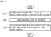
- FIG. 2 is a flowchart showing a method for preparing a multi-doped graphene according to an embodiment of the present invention.
- a step (S210) of mixing a metal-based dopant and at least one organic-based dopant is performed to prepare a doping solution.
- Graphene is doped with a metal-based dopant and an organic-based dopant all together. At this time, one metal-based dopant is used, and at least one organic-based dopant may be used.
- the metal-based dopant used according to the invention is AuCl 3 .
- Other useful metal-based dopants areHAuCl 4 , FeCl 3 , Ag compounds, Au compounds, or Pt compounds.
- the organic-based dopant used according to the invention is bis(trifluoromethanesulfonyl)imide, zinc di[bis(trifluoromethylsulfonyl)imide], or trifluoromethanesulfonyl chloride.
- organic-based dopants are bis(trifluoromethane)sulfonimide, silver(I) bis(trifluoromethanesulfonyl)imide, 1-(trifluoromethanesulfonyl)imidazole, N-(2-pyridyl) bis(trifluoromethanesulfonimide), bis(trifluoromethanesulfonyl)methane, N-(5-chloro-2-pyridyl)bis(trifluoromethanesulfonimide), N-phenyl-bis(trifluoromethanesulfonimide), methyl trifluoromethanesulfonate, trifluoromethanesulfonic anhydride, trifluoromethanesulfonamide, ethyl trifluoromethanesulfonate, zinc trifluoromethanesulfonate, tetracyanoethylene, 2,3,5,6-tetrafluoro-7,7
- a solvent for the doping solution may be an organic solvent.
- the solvent nitro methane, nitro benzene, or the like may be used.
- the metal-based dopant As the metal-based dopant, AuCl 3 is used, and as the organic-based dopant, bis(trifluoromethanesulfonyl)imide may be used. At this time, the metal-based dopant has a concentration of 1 to 10 mM, and the organic-based dopant has a concentration of 1 to 100 mM.
- the metal-based dopant As the metal-based dopant, AuCl 3 is used, and as the organic-based dopant, any one of zinc di[bis(trifluoromethylsulfonyl)imide] or trifluoromethanesulfonyl chloride may be used. At this time, the metal-based dopant has a concentration of 1 to 10 mM, and the organic-based dopant has a concentration of 1 to 200 mM.
- the metal-based dopant and two or more of the organic-based dopants may be mixed together in the doping solution.
- the doping solution may be composed of a mixture of the metal-based dopant, a first organic-based dopant, and a second organic-based dopant.
- AuCl 3 is used as the metal dopant
- bis(trifluoromethanesulfonyl)imide may be used as the first organic-based dopant
- any one of zinc di[bis(trifluoromethylsulfonyl)imide] or trifluoromethanesulfonyl chloride may be used as the second organic-based dopant.
- the metal-based dopant has a concentration of 1 to 10 mM
- the first organic-based dopant has a concentration of 1 to 100 mM
- the second organic-based dopant has a concentration of 1 to 200 mM.
- a step (S220) of synthesizing a graphene layer on a substrate is performed.
- stacking the graphene layer may be performed by a chemical vapor deposition (CVD) method.
- CVD chemical vapor deposition
- an already known method for preparing a graphene thin film may be utilized without being limited to CVD.
- a physical peel method, a chemical peel method, an epitaxial growth method, and the like may be utilized.
- CVD the method for synthesizing a graphene layer
- the substrate may vary depending on when doping in a series of steps of synthesizing a graphene layer is performed.
- the case of synthesizing a graphene layer using CVD will be explained as an example.
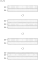
- FIGS. 3A and 3B are conceptual views showing a method for preparing a graphene layer using a chemical vapor deposition method.
- a graphene layer 320 is synthesized on a predetermined metal layer 310 in the CVD.
- the predetermined metal serves as a catalyst for synthesizing the graphene layer 320.
- the predetermined metal may be copper.
- Stacking a support layer 330 on the graphene layer 320 is performed.
- a Poly(methyl methacrylate) (PMMA) adhesive film, a UV film, a heat transfer film, and the like may be used.
- a support layer 330 is stacked on the graphene layer 320, and then removing the metal layer 310 is performed. At this time, the metal layer 310 may be removed by an etching method, and the like.
- the metal layer 310 is removed, and then doping may be performed on the graphene layer 320.
- the substrate may be the support layer 330.
- the doping result is illustrated as one layer 340 for convenience of explanation, but a separate layer may not be produced due to the doping of graphene.
- the metal layer 310 is removed, and then a graphene transfer layer 350 may be stacked on the graphene layer 320.
- the graphene transfer layer 350 may be PET and the like.
- the support layer 330 is removed.
- the support layer 330 is removed by using acetone, or removed by UV irradiation, or may be removed by adding heat thereto.
- the method of removing the support layer may vary depending on the material used as the support layer 330.
- the support layer 330 is removed, and then a doping 340 may be performed on the graphene layer 320.
- the substrate may be the graphene transfer layer.
- FIG. 3B illustrates the doping result as one layer 340 for convenience of explanation, but a separate layer may not be produced due to the doping of graphene.
- the doping of the graphene layer 320 may be performed immediately after the graphene layer is synthesized on the metal layer 310.
- the substrate may be a layer to which the graphene layer 320 is finally transferred.
- doping a graphene layer may be performed at any time after the graphene layer is synthesized.
- a step (S230) of doping the graphene layer with the doping solution that includes the metal-based dopant and the at least one organic-based dopant is performed.
- doping the graphene layer may be performed by any one of a spin coating, an immersion process, or a spray process.
- a doping solution is applied on a graphene layer in a state where a substrate and the graphene layer are rotated at a high speed. Thereafter, the graphene layer is dried under an air or nitrogen condition.
- the substrate and the graphene layer are immersed in the doping solution, and then dried under an air or nitrogen condition.
- the doping solution is sprayed onto the graphene layer by using a spray, and then the graphene layer is dried under an air or nitrogen atmosphere.
- a protective layer may be stacked on the graphene layer on which doping has been completed.
- the protective layer may be formed so as to protect the graphene layer from mechanical friction, and may be formed so as to prevent oxidation of a material doped on graphene.
- Graphene was prepared by using the above-described method for preparing graphene. At this time, as a dopant, two dopants (one metal-based dopant and one organic-based dopant) were used, and graphene was prepared by varying concentrations of the dopants dissolved in a doping solution.
- TFSI bis(trifluoromethanesulfonyl)imide
- Zn-(TFSI) 2 zinc di[bis(trifluoromethylsulfonyl)imide]
- TFSI -Cl trifluoromethanesulfonyl chloride
- Graphene was prepared by using the above-described method for preparing graphene. At this time, as a dopant, three dopants (one metal-based dopant and two organic-based dopants) were used, and graphene was prepared by varying concentrations of the dopants dissolved in a doping solution.
- Graphene was prepared by using the above-described method for preparing graphene. At this time, as the dopant, two organic dopants were used, and graphene was prepared by varying the concentrations of the dopants dissolved in a doping solution.
- Table 6 shows a rate of decrease in sheet resistance of graphene prepared by the above-described method. According to Table 6, it can be seen that when graphene is doped with the two organic dopants, the rate of decrease in sheet resistance is close to 0. [Table 6] TFSI Zn-(TFSI) 2 or TFSI -Cl Concentration (mM) 1 ⁇ 100 1 ⁇ 200 Rate of decrease 1 ⁇ 1.5%
- FIG. 4 is a graph showing a rate of decrease in sheet resistance of graphene during the single doping, the double-doping, and the triple-doping.
- the graphene used in the XPS analysis was a graphene single-doped with AuCl 3 and a graphene doped with AuCl 3 and an organic-based dopant TFSI all together.
- FIG. 5 is a graph showing the X-ray photoelectron spectroscopy results of single-doped and double-doped graphenes.
- TFSI does not directly work on the graphene, but serves as an assistant to increase the reduction potential of AuCl 3 , thereby increasing the effect of decreasing the sheet resistance.
Landscapes
- Chemical & Material Sciences (AREA)
- Organic Chemistry (AREA)
- Engineering & Computer Science (AREA)
- Materials Engineering (AREA)
- Nanotechnology (AREA)
- Inorganic Chemistry (AREA)
- Carbon And Carbon Compounds (AREA)
Description
- The present invention relates to a graphene doped with different dopants and a method for preparing the same.
- Graphitic carbon materials including fullerene, carbon nanotubes, and graphene as nano-materials composed only of carbon atoms have received much attention from the academic world and industries for their excellent electrical properties, and physical and chemical stability.
- In particular, graphene is a material which has come into the spotlight as an epoch-making new material due to the very high specific area compared with the volume, excellent electric conductivity, and physical and chemical stability.
- Meanwhile, studies have been experimentally conducted on doping into carbon lattices for several years. Doping is a process which may improve electrical properties such as sheet-resistance and charge mobility of graphene. When previous studies related to doping are reviewed, there are largely two methods, and examples thereof include a method in which doping is performed while graphene is synthesized, a method of modifying the material after graphene is synthesized, and the like.
- In particular, in order to reduce the sheet resistance of graphene in the related art, a technology of doping graphene with a metal-based dopant or an organic-based dopant has been used.
-
US 2011/0127471 describes a composition comprising graphene and a dopant including any one of organic and inorganic dopants.US 2011/0127471 also describes trifluoromethansulfoneimide as the organic dopant and AuCl3 as the inorganic dopant.US 2015/0162408 discloses a graphene film doped with an organic dopant, inorganic dopant or combinations of organic and inorganic dopants by roll-to-roll process. - Referring to
FIGS. 1A and 1B , there is a problem in that when graphene is doped with a predetermined amount or more of a metal-based dopant, graphene becomes reddened. Further, there is a problem in that when graphene is doped with a predetermined amount or more of an organic-based dopant, graphene and a substrate supporting graphene are damaged. - Meanwhile, referring to
FIGS. 1C and 1C , there is a problem in that when graphene is doped with a specific organic-based dopant, the sheet resistance of graphene is rather increased. - Due to the above-described problems, there is a limitation in reducing the sheet resistance of graphene through doping.
- Therefore, an aspect of the detailed description is to provide a graphene doping method that may prevent a reddening phenomenon which may occur due to a metal-based dopant, may minimize the damage of a substrate, which may occur due to an organic-based dopant, and may simultaneously minimize the sheet resistance of graphene. Another aspect of the detailed description is to provide a multi-doped graphene.
- The present disclosure provides a method for preparing a multi-doped graphene, the method including: mixing a metal-based dopant and at least one organic-based dopant to prepare a doping solution; stacking a graphene layer on a substrate; and doping the graphene layer with the doping solution that includes the metal-based dopant and the at least one organic-based dopant as defined in the claims.
- Further, the present disclosure provides a multi-doped graphene including a substrate; and a graphene layer formed on the substrate and doped with a metal-based dopant and an organic-based dopant as defined in the claims. In one aspect of the present invention, the multi-doped graphene may be prepared by the above described method.
- According to the present disclosure, it is possible to maintain the transparency of graphene and minimize the sheet resistance of graphene while not damaging a substrate on which the graphene is stacked.
- Further scope of applicability of the present application will become more apparent from the detailed description given hereinafter. However, it should be understood that the detailed description and specific examples, while indicating preferred embodiments of the disclosure, are given by way of illustration only.
- The accompanying drawings, which are included to provide a further understanding of the disclosure and are incorporated in and constitute a part of this specification, illustrate exemplary embodiments and together with the description serve to explain the principles of the disclosure.
-
FIGS. 1A to 1D are graphs showing a rate of decrease in graphene sheet resistance according to the concentration of a doping solution when graphene is doped with any one of a metal-based dopant and an organic-based dopant. -
FIG. 2 is a flowchart showing a method for preparing a multi-doped graphene according to an embodiment of the present invention. -
FIGS. 3A and3B are conceptual views showing a method for preparing a graphene layer using a chemical vapor deposition method according to an embodiment of the present invention. -
FIG. 4 is a graph showing a rate of decrease in sheet resistance of a doped graphene. -
FIG. 5 is a graph showing X-ray photoelectron spectroscopy (XPS) results of the doped graphene. - Description will now be given in detail according to exemplary embodiments disclosed herein, with reference to the accompanying drawings. For the sake of brief description with reference to the drawings, the same or equivalent components may be provided with the same or similar reference numbers, and description thereof will not be repeated. In general, a suffix such as "module" and "unit" may be used to refer to elements or components. Use of such a suffix herein is merely intended to facilitate description of the specification, and the suffix itself is not intended to give any special meaning or function. In the present disclosure, that which is well-known to one of ordinary skill in the relevant art has generally been omitted for the sake of brevity. The accompanying drawings are used to help easily understand various technical features and it should be understood that the embodiments presented herein are not limited by the accompanying drawings. As such, the present disclosure should be construed to extend to any alterations, equivalents and substitutes in addition to those which are particularly set out in the accompanying drawings.
- It will be understood that although the terms first, second, etc. may be used herein to describe various elements, these elements should not be limited by these terms. These terms are generally only used to distinguish one element from another.
- A singular representation may include a plural representation unless it represents a definitely different meaning from the context. Terms such as "include" or "has" are used herein and should be understood that they are intended to indicate an existence of several components, functions or steps, disclosed in the specification, and it is also understood that greater or fewer components, functions, or steps may likewise be utilized.
- Prior to explaining a multi-doped graphene according to the present invention and a method for preparing the same, a rate of decrease in sheet resistance of a single-doped graphene will be explained.
- The following Table 1 shows a rate of decrease in sheet resistance of graphene when the graphene is doped with a dopant solution having a predetermined concentration.
- Referring to Table 1, when graphene is doped by using a metal-based dopant AuCl3 and an organic-based dopant bis(trifluoromethanesulfonyl)imide, the higher the concentration of the dopant solution is, the higher the rate of decrease in sheet resistance of graphene is.
- However, when graphene is doped with AuCl3 at a concentration of 10 mM or more, a reddening phenomenon occurs, and when graphene is doped with a bis(trifluoromethanesulfonyl)imide solution at a concentration of 150 mM, a substrate is damaged by the dopant.
- Meanwhile, when graphene is doped with zinc di[bis(trifluoromethylsulfonyl)imide] and trifluoromethanesulfonyl chloride, the sheet resistance is rather increased.
[Table 1] High concentration AuCl3 (bis(trifluoro methanesulfo nyl)imide) Zinc di[bis(trifluoro methylsulfonyl )imide] Trifluoromethanes ulfonyl chloride Concentration 20 mM 20 mM 20 mM 20 mM Rate of decrease 70% 10% Increased by 5% Increased by 3 % Others When the concentration of AuCl3 is 10 mM or more, the rate of decrease is up to 70% or more, but the reddening phenomenon occurs When the graphene support layer is at a high concentration of 150 mM or more, the substrate is damaged by TFSI - According to Table 1, when graphene is doped with one dopant, the sheet resistance cannot be lowered to a predetermined level or less. In order to solve the above-described problem, one of embodiments of the present invention involves minimizing the sheet resistance of graphene by doping graphene with different dopants all together.
- Hereinafter, a method for preparing a multi-doped graphene according to an embodiment of the present invention will be described with reference to the accompanying drawings.
-
FIG. 2 is a flowchart showing a method for preparing a multi-doped graphene according to an embodiment of the present invention. - First, a step (S210) of mixing a metal-based dopant and at least one organic-based dopant is performed to prepare a doping solution. Graphene is doped with a metal-based dopant and an organic-based dopant all together. At this time, one metal-based dopant is used, and at least one organic-based dopant may be used.
- The metal-based dopant used according to the invention is AuCl3. Other useful metal-based dopants areHAuCl4, FeCl3, Ag compounds, Au compounds, or Pt compounds.
- The organic-based dopant used according to the invention is bis(trifluoromethanesulfonyl)imide, zinc di[bis(trifluoromethylsulfonyl)imide], or trifluoromethanesulfonyl chloride. Other useful organic-based dopants are bis(trifluoromethane)sulfonimide, silver(I) bis(trifluoromethanesulfonyl)imide, 1-(trifluoromethanesulfonyl)imidazole, N-(2-pyridyl) bis(trifluoromethanesulfonimide), bis(trifluoromethanesulfonyl)methane, N-(5-chloro-2-pyridyl)bis(trifluoromethanesulfonimide), N-phenyl-bis(trifluoromethanesulfonimide), methyl trifluoromethanesulfonate, trifluoromethanesulfonic anhydride, trifluoromethanesulfonamide, ethyl trifluoromethanesulfonate, zinc trifluoromethanesulfonate, tetracyanoethylene, 2,3,5,6-tetrafluoro-7,7,8,8-tetracyanoquinodimethane, potassium tetrafluoroborate, ammonium tetrafluoroborate, or ammonium hexafluorophosphate.
- A solvent for the doping solution may be an organic solvent. For example, as the solvent, nitro methane, nitro benzene, or the like may be used.
- As the metal-based dopant, AuCl3 is used, and as the organic-based dopant, bis(trifluoromethanesulfonyl)imide may be used. At this time, the metal-based dopant has a concentration of 1 to 10 mM, and the organic-based dopant has a concentration of 1 to 100 mM.
- As the metal-based dopant, AuCl3 is used, and as the organic-based dopant, any one of zinc di[bis(trifluoromethylsulfonyl)imide] or trifluoromethanesulfonyl chloride may be used. At this time, the metal-based dopant has a concentration of 1 to 10 mM, and the organic-based dopant has a concentration of 1 to 200 mM.
- According to an embodiment of the present invention, the metal-based dopant and two or more of the organic-based dopants may be mixed together in the doping solution.
- For example, the doping solution may be composed of a mixture of the metal-based dopant, a first organic-based dopant, and a second organic-based dopant. In one example, AuCl3 is used as the metal dopant, bis(trifluoromethanesulfonyl)imide may be used as the first organic-based dopant, and any one of zinc di[bis(trifluoromethylsulfonyl)imide] or trifluoromethanesulfonyl chloride may be used as the second organic-based dopant. At this time, the metal-based dopant has a concentration of 1 to 10 mM, the first organic-based dopant has a concentration of 1 to 100 mM, and the second organic-based dopant has a concentration of 1 to 200 mM.
- Meanwhile, apart from preparing the doping solution, a step (S220) of synthesizing a graphene layer on a substrate is performed.
- Here, stacking the graphene layer may be performed by a chemical vapor deposition (CVD) method. Meanwhile, in synthesizing the graphene layer, an already known method for preparing a graphene thin film may be utilized without being limited to CVD. Specifically, in the method for preparing a graphene layer, a physical peel method, a chemical peel method, an epitaxial growth method, and the like may be utilized.
- In the present specification, as the method for synthesizing a graphene layer, CVD will be explained as an example, but the method is not limited thereto.
- Meanwhile, the substrate may vary depending on when doping in a series of steps of synthesizing a graphene layer is performed. Hereinafter, the case of synthesizing a graphene layer using CVD will be explained as an example.
-
FIGS. 3A and3B are conceptual views showing a method for preparing a graphene layer using a chemical vapor deposition method. - Referring to
FIG. 3A , agraphene layer 320 is synthesized on apredetermined metal layer 310 in the CVD. Here, the predetermined metal serves as a catalyst for synthesizing thegraphene layer 320. The predetermined metal may be copper. - Stacking a
support layer 330 on thegraphene layer 320 is performed. As thesupport layer 330, a Poly(methyl methacrylate) (PMMA) adhesive film, a UV film, a heat transfer film, and the like may be used. - A
support layer 330 is stacked on thegraphene layer 320, and then removing themetal layer 310 is performed. At this time, themetal layer 310 may be removed by an etching method, and the like. - The
metal layer 310 is removed, and then doping may be performed on thegraphene layer 320. In this case, the substrate may be thesupport layer 330. InFIG. 3A , the doping result is illustrated as onelayer 340 for convenience of explanation, but a separate layer may not be produced due to the doping of graphene. - Meanwhile, referring to
FIG. 3B , themetal layer 310 is removed, and then agraphene transfer layer 350 may be stacked on thegraphene layer 320. Here, thegraphene transfer layer 350 may be PET and the like. - Thereafter, the
support layer 330 is removed. At this time, thesupport layer 330 is removed by using acetone, or removed by UV irradiation, or may be removed by adding heat thereto. The method of removing the support layer may vary depending on the material used as thesupport layer 330. - The
support layer 330 is removed, and then adoping 340 may be performed on thegraphene layer 320. In this case, the substrate may be the graphene transfer layer.FIG. 3B illustrates the doping result as onelayer 340 for convenience of explanation, but a separate layer may not be produced due to the doping of graphene. - Meanwhile, the doping of the
graphene layer 320 may be performed immediately after the graphene layer is synthesized on themetal layer 310. In this case, the substrate may be a layer to which thegraphene layer 320 is finally transferred. - As described above, doping a graphene layer may be performed at any time after the graphene layer is synthesized.
- Next, a step (S230) of doping the graphene layer with the doping solution that includes the metal-based dopant and the at least one organic-based dopant is performed. Here, doping the graphene layer may be performed by any one of a spin coating, an immersion process, or a spray process.
- In the case of a spin coating method, a doping solution is applied on a graphene layer in a state where a substrate and the graphene layer are rotated at a high speed. Thereafter, the graphene layer is dried under an air or nitrogen condition.
- In the case of an immersion process, the substrate and the graphene layer are immersed in the doping solution, and then dried under an air or nitrogen condition.
- In the case of a spray process, the doping solution is sprayed onto the graphene layer by using a spray, and then the graphene layer is dried under an air or nitrogen atmosphere.
- Meanwhile, a protective layer may be stacked on the graphene layer on which doping has been completed. The protective layer may be formed so as to protect the graphene layer from mechanical friction, and may be formed so as to prevent oxidation of a material doped on graphene.
- Hereinafter, embodiments of the present invention will be described in more detail through the Examples and the Experimental Examples. However, the scope and content of the present invention are not interpreted to be curtailed or limited by the Examples and the Experimental Examples to be described below.
- Graphene was prepared by using the above-described method for preparing graphene. At this time, as a dopant, two dopants (one metal-based dopant and one organic-based dopant) were used, and graphene was prepared by varying concentrations of the dopants dissolved in a doping solution.
- The following tables show a rate of decrease in sheet resistance of graphene prepared by the above-described method. In the following tables, bis(trifluoromethanesulfonyl)imide is represented by TFSI, zinc di[bis(trifluoromethylsulfonyl)imide] is represented by Zn-(TFSI)2, and trifluoromethanesulfonyl chloride is represented by TFSI -Cl.
[Table 2] AuCl3 TFSI Concentration (mM) 1 ∼ 10 1 ∼ 100 Rate of decrease 40 ∼ 52% [Table 3] AuCl3 Zn-(TFSI)2 or TFSI -Cl Concentration (mM) 1 ∼ 10 1 ∼ 200 Rate of decrease 40 ∼ 52% - Referring to Tables 2 and 3, it can be confirmed that when the graphene layer is doped with a metal-based dopant and an organic-based dopant all together, a higher rate of decrease in sheet resistance may be exhibited by using a doping solution even at a lower concentration than that shown in Table 1.
- Graphene was prepared by using the above-described method for preparing graphene. At this time, as a dopant, three dopants (one metal-based dopant and two organic-based dopants) were used, and graphene was prepared by varying concentrations of the dopants dissolved in a doping solution.
- The following tables show a rate of decrease in sheet resistance of graphene prepared by the above-described method.
[Table 4] AuCl3 TFSI Zn-(TFSI)2 Concentration (mM) 1 ∼ 10 0.2 ∼ 100 0.2 ∼ 200 Rate of decrease 50 - 70 % [Table 5] AuCl3 TFSI TFSI - Cl Concentration (mM) 1 ∼ 10 1 ∼ 100 0.2 ∼ 200 Rate of decrease 50 - 70 % - Referring to Tables 4 and 5, it can be confirmed that the three dopants have a higher rate of decrease in sheet resistance than those of the two dopants.
- Graphene was prepared by using the above-described method for preparing graphene. At this time, as the dopant, two organic dopants were used, and graphene was prepared by varying the concentrations of the dopants dissolved in a doping solution.
- The following Table 6 shows a rate of decrease in sheet resistance of graphene prepared by the above-described method. According to Table 6, it can be seen that when graphene is doped with the two organic dopants, the rate of decrease in sheet resistance is close to 0.
[Table 6] TFSI Zn-(TFSI)2 or TFSI -Cl Concentration (mM) 1 ∼ 100 1 ∼ 200 Rate of decrease 1 ∼ 1.5% - Meanwhile,
FIG. 4 is a graph showing a rate of decrease in sheet resistance of graphene during the single doping, the double-doping, and the triple-doping. - Referring to Tables 1 to 5 and
FIG. 4 , when graphene is doped with a metal-based dopant and at least one organic-based dopant all together, a high rate of decrease in sheet resistance is exhibited even at a relatively low dopant concentration. Accordingly, it is possible to significantly decrease the sheet resistance of graphene and simultaneously prevent the reddening phenomenon and the damage of a substrate according to the doping. - In order to check an effect of an organic-based dopant to dope graphene together with a metal-based dopant, the content of a metal in a reduced state present in doped graphene was measured. For this purpose, graphene of which doping has been completed was analyzed by an X-ray photoelectron spectroscopy (XPS).
- Here, the graphene used in the XPS analysis was a graphene single-doped with AuCl3 and a graphene doped with AuCl3 and an organic-based dopant TFSI all together.
-
FIG. 5 is a graph showing the X-ray photoelectron spectroscopy results of single-doped and double-doped graphenes. - Referring to
FIG. 5 , in the case of graphene single-doped with AuCl3, the content of Au(AuO) in a reduced state was 15.7%. In contrast, in the case of graphene doped with AuCl3 and TFSI all together, the content of AuO was 26.8%. - According to the above-described XPS analysis results, TFSI does not directly work on the graphene, but serves as an assistant to increase the reduction potential of AuCl3, thereby increasing the effect of decreasing the sheet resistance.
- The foregoing embodiments and advantages are merely exemplary and are not to be considered as limiting the present disclosure. The present teachings can be readily applied to other types of apparatuses. This description is intended to be illustrative, and not to limit the scope of the claims. Many alternatives, modifications, and variations will be apparent to those skilled in the art. The features, structures, methods, and other characteristics of the exemplary embodiments described herein may be combined in various ways to obtain additional and/or alternative exemplary embodiments.
- As the present features may be embodied in several forms without departing from the characteristics thereof, it should also be understood that the above-described embodiments are not limited by any of the details of the foregoing description, unless otherwise specified, but rather should be considered broadly within its scope as defined in the appended claims, and therefore all changes and modifications that fall within the metes and bounds of the claims, or equivalents of such metes and bounds are therefore intended to be embraced by the appended claims.
Claims (3)
- A method for preparing a multi-doped graphene, the method comprising:mixing a metal-based dopant and at least one organic-based dopant to prepare a doping solution;stacking a graphene layer on a substrate; anddoping the graphene layer with the doping solution that includes the metal-based dopant and the at least one organic-based dopant,wherein the metal-based dopant is AuCl3 and a concentration of AuCl3 in the doping solution is 1 to 10 mM; andwherein the at least one organic-based dopant isbis(trifluoromethanesulfonyl)imide and a concentration of bis(trifluoromethanesulfonyl)imide in the doping solution is 1 to 100 mM, or any one of zinc di[bis(trifluoromethylsulfonyl)imide] or trifluoromethanesulfonyl chloride and a concentration of zinc di[bis(trifluoromethylsulfonyl)imide] or trifluoromethanesulfonyl chloride in the doping solution is 1 to 200 mM.
- The method of claim 1, wherein the doping solution comprises a mixture of the metal-based dopant, a first organic-based dopant, and a second organic-based dopant,wherein the metal-based dopant is AuCl3 and a concentration of AuCl3 in the doping solution is 1 to 10 mM;the first organic-based dopant is bis(trifluoromethanesulfonyl)imide and a concentration of bis(trifluoromethanesulfonyl)imide in the doping solution is 1 to 100 mM; andthe second organic-based dopant is any one of zinc di[bis(trifluoromethylsulfonyl)imide] or trifluoromethanesulfonyl chloride and a concentration of zinc di[bis(trifluoromethylsulfonyl)imide] or trifluoromethanesulfonyl chloride in the doping solution is 1 to 200 mM.
- A multi-doped graphene comprising:a substrate; anda graphene layer formed on the substrate and doped with a metal-based dopant, a first organic-based dopant and a second organic-based dopant, wherein the metal-based dopant is AuCl3;the first organic-based dopant is bis(trifluoromethanesulfonyl)imide; andthe second organic-based dopant is any one of zinc di[bis(trifluoromethylsulfonyl)imide] or trifluoromethanesulfonyl chloride.
Applications Claiming Priority (2)
| Application Number | Priority Date | Filing Date | Title |
|---|---|---|---|
| KR1020160115130A KR102642749B1 (en) | 2016-09-07 | 2016-09-07 | Multi-doped graphene and method for producing the same |
| PCT/KR2017/005006 WO2018048059A1 (en) | 2016-09-07 | 2017-05-15 | Multi-doped graphene and method for preparing the same |
Publications (3)
| Publication Number | Publication Date |
|---|---|
| EP3509988A1 EP3509988A1 (en) | 2019-07-17 |
| EP3509988A4 EP3509988A4 (en) | 2020-05-06 |
| EP3509988B1 true EP3509988B1 (en) | 2023-04-12 |
Family
ID=61280821
Family Applications (1)
| Application Number | Title | Priority Date | Filing Date |
|---|---|---|---|
| EP17848944.9A Active EP3509988B1 (en) | 2016-09-07 | 2017-05-15 | Multi-doped graphene and method for preparing the same |
Country Status (5)
| Country | Link |
|---|---|
| US (1) | US10361275B2 (en) |
| EP (1) | EP3509988B1 (en) |
| KR (1) | KR102642749B1 (en) |
| CN (1) | CN109661369B (en) |
| WO (1) | WO2018048059A1 (en) |
Families Citing this family (4)
| Publication number | Priority date | Publication date | Assignee | Title |
|---|---|---|---|---|
| US11127509B2 (en) | 2016-10-11 | 2021-09-21 | Ultraconductive Copper Company Inc. | Graphene-copper composite structure and manufacturing method |
| US10828869B2 (en) * | 2017-08-30 | 2020-11-10 | Ultra Conductive Copper Company, Inc. | Graphene-copper structure and manufacturing method |
| KR102534569B1 (en) * | 2019-12-30 | 2023-05-22 | 한국전자통신연구원 | Semiconductor material and manufacturing method thereof |
| CN111410872B (en) * | 2020-04-15 | 2022-05-31 | 广东康烯科技有限公司 | Preparation method of platinum quantum dot doped graphene-based conductive ink, conductive ink and application |
Family Cites Families (11)
| Publication number | Priority date | Publication date | Assignee | Title |
|---|---|---|---|---|
| KR20110061909A (en) * | 2009-12-02 | 2011-06-10 | 삼성전자주식회사 | Graphene doped with dopant and device using same |
| WO2011081440A2 (en) * | 2009-12-30 | 2011-07-07 | 성균관대학교산학협력단 | Roll-to-roll doping method of graphene film, and doped graphene film |
| CN102142294A (en) * | 2010-01-29 | 2011-08-03 | 海洋王照明科技股份有限公司 | Graphene-ionic liquid composite material and preparation method thereof |
| WO2011108878A2 (en) | 2010-03-05 | 2011-09-09 | 성균관대학교산학협력단 | Electromagnetic shielding method using graphene and electromagnetic shielding material |
| US10177261B2 (en) * | 2010-10-05 | 2019-01-08 | Samsung Electronics Co., Ltd. | Transparent electrode comprising doped graphene, process of preparing the same, and display device and solar cell comprising the electrode |
| KR101802374B1 (en) * | 2010-10-05 | 2017-11-29 | 삼성전자주식회사 | Transparent electrode comprising doped graphene, process for preparing the same, and display device and solar cell comprising the electrode |
| KR101469450B1 (en) * | 2011-03-02 | 2014-12-05 | 그래핀스퀘어 주식회사 | N-doping method of graphene |
| KR102014993B1 (en) * | 2012-10-23 | 2019-08-27 | 삼성전자주식회사 | Doped graphene composition comprising hydrophobic organics, process for preparing the same, and transparent electrode, display device and solar cell comprising the electrode |
| CN104409177B (en) * | 2014-11-28 | 2017-02-22 | 中国科学院金属研究所 | Large-scale preparation method for stably-doped large-area graphene transparent conductive films |
| CN104528699B (en) * | 2014-12-22 | 2016-05-11 | 中国科学院重庆绿色智能技术研究院 | A kind of stable doping method of graphene film |
| CN104528698B (en) * | 2014-12-22 | 2016-06-08 | 重庆墨希科技有限公司 | A kind of stable doping method of Graphene |
-
2016
- 2016-09-07 KR KR1020160115130A patent/KR102642749B1/en active Active
-
2017
- 2017-03-10 US US15/456,421 patent/US10361275B2/en active Active
- 2017-05-15 CN CN201780054618.8A patent/CN109661369B/en active Active
- 2017-05-15 EP EP17848944.9A patent/EP3509988B1/en active Active
- 2017-05-15 WO PCT/KR2017/005006 patent/WO2018048059A1/en not_active Ceased
Also Published As
| Publication number | Publication date |
|---|---|
| EP3509988A1 (en) | 2019-07-17 |
| KR102642749B1 (en) | 2024-03-04 |
| CN109661369B (en) | 2022-10-18 |
| EP3509988A4 (en) | 2020-05-06 |
| WO2018048059A1 (en) | 2018-03-15 |
| US10361275B2 (en) | 2019-07-23 |
| KR20180027899A (en) | 2018-03-15 |
| US20180069082A1 (en) | 2018-03-08 |
| CN109661369A (en) | 2019-04-19 |
Similar Documents
| Publication | Publication Date | Title |
|---|---|---|
| Yoo et al. | Efficient perovskite solar mini-modules fabricated via bar-coating using 2-methoxyethanol-based formamidinium lead tri-iodide precursor solution | |
| Yao et al. | Fluorinated Perylene‐Diimides: Cathode Interlayers Facilitating Carrier Collection for High‐Performance Organic Solar Cells | |
| Lin et al. | Ionic liquid-induced ostwald ripening effect for efficient and stable tin-based perovskite solar cells | |
| Mahmood et al. | 16.1% Efficient hysteresis‐free mesostructured perovskite solar cells based on synergistically improved ZnO nanorod arrays | |
| Ercan et al. | A Redox‐Based Resistive Switching Memory Device Consisting of Organic–Inorganic Hybrid Perovskite/Polymer Composite Thin Film | |
| Liang et al. | CsPb0. 9Sn0. 1IBr2 based all-inorganic perovskite solar cells with exceptional efficiency and stability | |
| Thiemann et al. | Ionic liquids for electrolyte-gating of ZnO field-effect transistors | |
| JP5753584B2 (en) | Method for increasing the conductivity of graphene films | |
| EP2002492B1 (en) | Use of heterocyclic radicals for doping organic semiconductors | |
| EP1786050B1 (en) | Doped organic semiconductor material | |
| Dualeh et al. | Temperature dependence of transport properties of spiro-MeOTAD as a hole transport material in solid-state dye-sensitized solar cells | |
| Ma et al. | Pushing the conductance and transparency limit of monolayer graphene electrodes for flexible organic light-emitting diodes | |
| US9162883B2 (en) | Doped carbon nanotubes and transparent conducting films containing the same | |
| Zhou et al. | High-mobility and bias-stable field-effect transistors based on lead-free formamidinium tin iodide perovskites | |
| Higgins et al. | Dopant controlled trap-filling and conductivity enhancement in an electron-transport polymer | |
| US10361275B2 (en) | Multi-doped graphene and method for preparing the same | |
| EP2911977B1 (en) | Transparent electrode comprising a doped graphene structure and method for preparing the same | |
| CN102947414A (en) | Doping material for hole conducting layer of organic semiconductor device and its application | |
| Lu et al. | Pursuing high‐performance organic field‐effect transistors through organic salt doping | |
| Ali et al. | A simple Cu (II) polyelectrolyte as a method to increase the work function of electrodes and form effective p‐type contacts in perovskite solar cells | |
| US20130040146A1 (en) | Graphene structure and roduction method thereof | |
| Cho et al. | Anion‐Vacancy‐Defect Passivation of a 2D‐Layered Tin‐Based Perovskite Thin‐Film Transistor with Sulfur Doping | |
| US20150064839A1 (en) | Method of forming tin oxide semiconductor thin film | |
| KR101984930B1 (en) | Graphene laminate comprising reduced graphene oxide, method for manufacturing same, eletrode material using same, and electronic device | |
| Chen et al. | Effective Defect Passivation via Molecular Interactions Based on Amine-Functionalized Ionic Liquid for Perovskite Solar Cells |
Legal Events
| Date | Code | Title | Description |
|---|---|---|---|
| STAA | Information on the status of an ep patent application or granted ep patent |
Free format text: STATUS: THE INTERNATIONAL PUBLICATION HAS BEEN MADE |
|
| PUAI | Public reference made under article 153(3) epc to a published international application that has entered the european phase |
Free format text: ORIGINAL CODE: 0009012 |
|
| STAA | Information on the status of an ep patent application or granted ep patent |
Free format text: STATUS: REQUEST FOR EXAMINATION WAS MADE |
|
| 17P | Request for examination filed |
Effective date: 20190328 |
|
| AK | Designated contracting states |
Kind code of ref document: A1 Designated state(s): AL AT BE BG CH CY CZ DE DK EE ES FI FR GB GR HR HU IE IS IT LI LT LU LV MC MK MT NL NO PL PT RO RS SE SI SK SM TR |
|
| AX | Request for extension of the european patent |
Extension state: BA ME |
|
| DAV | Request for validation of the european patent (deleted) | ||
| DAX | Request for extension of the european patent (deleted) | ||
| A4 | Supplementary search report drawn up and despatched |
Effective date: 20200403 |
|
| RIC1 | Information provided on ipc code assigned before grant |
Ipc: H01L 29/167 20060101ALI20200330BHEP Ipc: C01B 32/182 20170101AFI20200330BHEP Ipc: C01B 32/194 20170101ALI20200330BHEP |
|
| GRAP | Despatch of communication of intention to grant a patent |
Free format text: ORIGINAL CODE: EPIDOSNIGR1 |
|
| STAA | Information on the status of an ep patent application or granted ep patent |
Free format text: STATUS: GRANT OF PATENT IS INTENDED |
|
| INTG | Intention to grant announced |
Effective date: 20221111 |
|
| GRAS | Grant fee paid |
Free format text: ORIGINAL CODE: EPIDOSNIGR3 |
|
| GRAA | (expected) grant |
Free format text: ORIGINAL CODE: 0009210 |
|
| STAA | Information on the status of an ep patent application or granted ep patent |
Free format text: STATUS: THE PATENT HAS BEEN GRANTED |
|
| AK | Designated contracting states |
Kind code of ref document: B1 Designated state(s): AL AT BE BG CH CY CZ DE DK EE ES FI FR GB GR HR HU IE IS IT LI LT LU LV MC MK MT NL NO PL PT RO RS SE SI SK SM TR |
|
| REG | Reference to a national code |
Ref country code: GB Ref legal event code: FG4D |
|
| REG | Reference to a national code |
Ref country code: CH Ref legal event code: EP |
|
| REG | Reference to a national code |
Ref country code: DE Ref legal event code: R096 Ref document number: 602017067717 Country of ref document: DE |
|
| REG | Reference to a national code |
Ref country code: IE Ref legal event code: FG4D |
|
| REG | Reference to a national code |
Ref country code: AT Ref legal event code: REF Ref document number: 1559691 Country of ref document: AT Kind code of ref document: T Effective date: 20230515 |
|
| REG | Reference to a national code |
Ref country code: LT Ref legal event code: MG9D |
|
| REG | Reference to a national code |
Ref country code: NL Ref legal event code: MP Effective date: 20230412 |
|
| REG | Reference to a national code |
Ref country code: AT Ref legal event code: MK05 Ref document number: 1559691 Country of ref document: AT Kind code of ref document: T Effective date: 20230412 |
|
| PG25 | Lapsed in a contracting state [announced via postgrant information from national office to epo] |
Ref country code: NL Free format text: LAPSE BECAUSE OF FAILURE TO SUBMIT A TRANSLATION OF THE DESCRIPTION OR TO PAY THE FEE WITHIN THE PRESCRIBED TIME-LIMIT Effective date: 20230412 |
|
| PG25 | Lapsed in a contracting state [announced via postgrant information from national office to epo] |
Ref country code: SE Free format text: LAPSE BECAUSE OF FAILURE TO SUBMIT A TRANSLATION OF THE DESCRIPTION OR TO PAY THE FEE WITHIN THE PRESCRIBED TIME-LIMIT Effective date: 20230412 Ref country code: PT Free format text: LAPSE BECAUSE OF FAILURE TO SUBMIT A TRANSLATION OF THE DESCRIPTION OR TO PAY THE FEE WITHIN THE PRESCRIBED TIME-LIMIT Effective date: 20230814 Ref country code: NO Free format text: LAPSE BECAUSE OF FAILURE TO SUBMIT A TRANSLATION OF THE DESCRIPTION OR TO PAY THE FEE WITHIN THE PRESCRIBED TIME-LIMIT Effective date: 20230712 Ref country code: ES Free format text: LAPSE BECAUSE OF FAILURE TO SUBMIT A TRANSLATION OF THE DESCRIPTION OR TO PAY THE FEE WITHIN THE PRESCRIBED TIME-LIMIT Effective date: 20230412 Ref country code: AT Free format text: LAPSE BECAUSE OF FAILURE TO SUBMIT A TRANSLATION OF THE DESCRIPTION OR TO PAY THE FEE WITHIN THE PRESCRIBED TIME-LIMIT Effective date: 20230412 |
|
| PG25 | Lapsed in a contracting state [announced via postgrant information from national office to epo] |
Ref country code: RS Free format text: LAPSE BECAUSE OF FAILURE TO SUBMIT A TRANSLATION OF THE DESCRIPTION OR TO PAY THE FEE WITHIN THE PRESCRIBED TIME-LIMIT Effective date: 20230412 Ref country code: PL Free format text: LAPSE BECAUSE OF FAILURE TO SUBMIT A TRANSLATION OF THE DESCRIPTION OR TO PAY THE FEE WITHIN THE PRESCRIBED TIME-LIMIT Effective date: 20230412 Ref country code: LV Free format text: LAPSE BECAUSE OF FAILURE TO SUBMIT A TRANSLATION OF THE DESCRIPTION OR TO PAY THE FEE WITHIN THE PRESCRIBED TIME-LIMIT Effective date: 20230412 Ref country code: LT Free format text: LAPSE BECAUSE OF FAILURE TO SUBMIT A TRANSLATION OF THE DESCRIPTION OR TO PAY THE FEE WITHIN THE PRESCRIBED TIME-LIMIT Effective date: 20230412 Ref country code: IS Free format text: LAPSE BECAUSE OF FAILURE TO SUBMIT A TRANSLATION OF THE DESCRIPTION OR TO PAY THE FEE WITHIN THE PRESCRIBED TIME-LIMIT Effective date: 20230812 Ref country code: HR Free format text: LAPSE BECAUSE OF FAILURE TO SUBMIT A TRANSLATION OF THE DESCRIPTION OR TO PAY THE FEE WITHIN THE PRESCRIBED TIME-LIMIT Effective date: 20230412 Ref country code: GR Free format text: LAPSE BECAUSE OF FAILURE TO SUBMIT A TRANSLATION OF THE DESCRIPTION OR TO PAY THE FEE WITHIN THE PRESCRIBED TIME-LIMIT Effective date: 20230713 Ref country code: AL Free format text: LAPSE BECAUSE OF FAILURE TO SUBMIT A TRANSLATION OF THE DESCRIPTION OR TO PAY THE FEE WITHIN THE PRESCRIBED TIME-LIMIT Effective date: 20230412 |
|
| PG25 | Lapsed in a contracting state [announced via postgrant information from national office to epo] |
Ref country code: FI Free format text: LAPSE BECAUSE OF FAILURE TO SUBMIT A TRANSLATION OF THE DESCRIPTION OR TO PAY THE FEE WITHIN THE PRESCRIBED TIME-LIMIT Effective date: 20230412 |
|
| REG | Reference to a national code |
Ref country code: CH Ref legal event code: PL |
|
| REG | Reference to a national code |
Ref country code: DE Ref legal event code: R097 Ref document number: 602017067717 Country of ref document: DE |
|
| PG25 | Lapsed in a contracting state [announced via postgrant information from national office to epo] |
Ref country code: SK Free format text: LAPSE BECAUSE OF FAILURE TO SUBMIT A TRANSLATION OF THE DESCRIPTION OR TO PAY THE FEE WITHIN THE PRESCRIBED TIME-LIMIT Effective date: 20230412 |
|
| PG25 | Lapsed in a contracting state [announced via postgrant information from national office to epo] |
Ref country code: MC Free format text: LAPSE BECAUSE OF FAILURE TO SUBMIT A TRANSLATION OF THE DESCRIPTION OR TO PAY THE FEE WITHIN THE PRESCRIBED TIME-LIMIT Effective date: 20230412 |
|
| REG | Reference to a national code |
Ref country code: BE Ref legal event code: MM Effective date: 20230531 |
|
| PG25 | Lapsed in a contracting state [announced via postgrant information from national office to epo] |
Ref country code: SM Free format text: LAPSE BECAUSE OF FAILURE TO SUBMIT A TRANSLATION OF THE DESCRIPTION OR TO PAY THE FEE WITHIN THE PRESCRIBED TIME-LIMIT Effective date: 20230412 Ref country code: SK Free format text: LAPSE BECAUSE OF FAILURE TO SUBMIT A TRANSLATION OF THE DESCRIPTION OR TO PAY THE FEE WITHIN THE PRESCRIBED TIME-LIMIT Effective date: 20230412 Ref country code: RO Free format text: LAPSE BECAUSE OF FAILURE TO SUBMIT A TRANSLATION OF THE DESCRIPTION OR TO PAY THE FEE WITHIN THE PRESCRIBED TIME-LIMIT Effective date: 20230412 Ref country code: MC Free format text: LAPSE BECAUSE OF FAILURE TO SUBMIT A TRANSLATION OF THE DESCRIPTION OR TO PAY THE FEE WITHIN THE PRESCRIBED TIME-LIMIT Effective date: 20230412 Ref country code: LU Free format text: LAPSE BECAUSE OF NON-PAYMENT OF DUE FEES Effective date: 20230515 Ref country code: LI Free format text: LAPSE BECAUSE OF NON-PAYMENT OF DUE FEES Effective date: 20230531 Ref country code: EE Free format text: LAPSE BECAUSE OF FAILURE TO SUBMIT A TRANSLATION OF THE DESCRIPTION OR TO PAY THE FEE WITHIN THE PRESCRIBED TIME-LIMIT Effective date: 20230412 Ref country code: DK Free format text: LAPSE BECAUSE OF FAILURE TO SUBMIT A TRANSLATION OF THE DESCRIPTION OR TO PAY THE FEE WITHIN THE PRESCRIBED TIME-LIMIT Effective date: 20230412 Ref country code: CZ Free format text: LAPSE BECAUSE OF FAILURE TO SUBMIT A TRANSLATION OF THE DESCRIPTION OR TO PAY THE FEE WITHIN THE PRESCRIBED TIME-LIMIT Effective date: 20230412 Ref country code: CH Free format text: LAPSE BECAUSE OF NON-PAYMENT OF DUE FEES Effective date: 20230531 |
|
| PLBE | No opposition filed within time limit |
Free format text: ORIGINAL CODE: 0009261 |
|
| STAA | Information on the status of an ep patent application or granted ep patent |
Free format text: STATUS: NO OPPOSITION FILED WITHIN TIME LIMIT |
|
| REG | Reference to a national code |
Ref country code: IE Ref legal event code: MM4A |
|
| 26N | No opposition filed |
Effective date: 20240115 |
|
| PG25 | Lapsed in a contracting state [announced via postgrant information from national office to epo] |
Ref country code: IE Free format text: LAPSE BECAUSE OF NON-PAYMENT OF DUE FEES Effective date: 20230515 |
|
| PG25 | Lapsed in a contracting state [announced via postgrant information from national office to epo] |
Ref country code: IE Free format text: LAPSE BECAUSE OF NON-PAYMENT OF DUE FEES Effective date: 20230515 |
|
| PG25 | Lapsed in a contracting state [announced via postgrant information from national office to epo] |
Ref country code: SI Free format text: LAPSE BECAUSE OF FAILURE TO SUBMIT A TRANSLATION OF THE DESCRIPTION OR TO PAY THE FEE WITHIN THE PRESCRIBED TIME-LIMIT Effective date: 20230412 |
|
| PG25 | Lapsed in a contracting state [announced via postgrant information from national office to epo] |
Ref country code: SI Free format text: LAPSE BECAUSE OF FAILURE TO SUBMIT A TRANSLATION OF THE DESCRIPTION OR TO PAY THE FEE WITHIN THE PRESCRIBED TIME-LIMIT Effective date: 20230412 Ref country code: IT Free format text: LAPSE BECAUSE OF FAILURE TO SUBMIT A TRANSLATION OF THE DESCRIPTION OR TO PAY THE FEE WITHIN THE PRESCRIBED TIME-LIMIT Effective date: 20230412 Ref country code: BE Free format text: LAPSE BECAUSE OF NON-PAYMENT OF DUE FEES Effective date: 20230531 |
|
| PG25 | Lapsed in a contracting state [announced via postgrant information from national office to epo] |
Ref country code: BG Free format text: LAPSE BECAUSE OF FAILURE TO SUBMIT A TRANSLATION OF THE DESCRIPTION OR TO PAY THE FEE WITHIN THE PRESCRIBED TIME-LIMIT Effective date: 20230412 |
|
| PG25 | Lapsed in a contracting state [announced via postgrant information from national office to epo] |
Ref country code: BG Free format text: LAPSE BECAUSE OF FAILURE TO SUBMIT A TRANSLATION OF THE DESCRIPTION OR TO PAY THE FEE WITHIN THE PRESCRIBED TIME-LIMIT Effective date: 20230412 |
|
| PGFP | Annual fee paid to national office [announced via postgrant information from national office to epo] |
Ref country code: DE Payment date: 20250407 Year of fee payment: 9 |
|
| PGFP | Annual fee paid to national office [announced via postgrant information from national office to epo] |
Ref country code: FR Payment date: 20250408 Year of fee payment: 9 |
|
| PG25 | Lapsed in a contracting state [announced via postgrant information from national office to epo] |
Ref country code: CY Free format text: LAPSE BECAUSE OF FAILURE TO SUBMIT A TRANSLATION OF THE DESCRIPTION OR TO PAY THE FEE WITHIN THE PRESCRIBED TIME-LIMIT; INVALID AB INITIO Effective date: 20170515 |
|
| PG25 | Lapsed in a contracting state [announced via postgrant information from national office to epo] |
Ref country code: HU Free format text: LAPSE BECAUSE OF FAILURE TO SUBMIT A TRANSLATION OF THE DESCRIPTION OR TO PAY THE FEE WITHIN THE PRESCRIBED TIME-LIMIT; INVALID AB INITIO Effective date: 20170515 |
|
| PG25 | Lapsed in a contracting state [announced via postgrant information from national office to epo] |
Ref country code: TR Free format text: LAPSE BECAUSE OF FAILURE TO SUBMIT A TRANSLATION OF THE DESCRIPTION OR TO PAY THE FEE WITHIN THE PRESCRIBED TIME-LIMIT Effective date: 20230412 |
|
| PGFP | Annual fee paid to national office [announced via postgrant information from national office to epo] |
Ref country code: GB Payment date: 20260309 Year of fee payment: 10 |