EP3509215A2 - Wireless system having local oscillator signal derived from reference clock output of active oscillator that has no electromechanical resonator - Google Patents
Wireless system having local oscillator signal derived from reference clock output of active oscillator that has no electromechanical resonator Download PDFInfo
- Publication number
- EP3509215A2 EP3509215A2 EP18202444.8A EP18202444A EP3509215A2 EP 3509215 A2 EP3509215 A2 EP 3509215A2 EP 18202444 A EP18202444 A EP 18202444A EP 3509215 A2 EP3509215 A2 EP 3509215A2
- Authority
- EP
- European Patent Office
- Prior art keywords
- frequency
- wireless system
- reference clock
- chip
- clock
- Prior art date
- Legal status (The legal status is an assumption and is not a legal conclusion. Google has not performed a legal analysis and makes no representation as to the accuracy of the status listed.)
- Granted
Links
Images




Classifications
-
- H—ELECTRICITY
- H04—ELECTRIC COMMUNICATION TECHNIQUE
- H04B—TRANSMISSION
- H04B1/00—Details of transmission systems, not covered by a single one of groups H04B3/00 - H04B13/00; Details of transmission systems not characterised by the medium used for transmission
- H04B1/38—Transceivers, i.e. devices in which transmitter and receiver form a structural unit and in which at least one part is used for functions of transmitting and receiving
- H04B1/40—Circuits
- H04B1/403—Circuits using the same oscillator for generating both the transmitter frequency and the receiver local oscillator frequency
-
- H—ELECTRICITY
- H04—ELECTRIC COMMUNICATION TECHNIQUE
- H04B—TRANSMISSION
- H04B1/00—Details of transmission systems, not covered by a single one of groups H04B3/00 - H04B13/00; Details of transmission systems not characterised by the medium used for transmission
- H04B1/38—Transceivers, i.e. devices in which transmitter and receiver form a structural unit and in which at least one part is used for functions of transmitting and receiving
- H04B1/40—Circuits
-
- G—PHYSICS
- G01—MEASURING; TESTING
- G01S—RADIO DIRECTION-FINDING; RADIO NAVIGATION; DETERMINING DISTANCE OR VELOCITY BY USE OF RADIO WAVES; LOCATING OR PRESENCE-DETECTING BY USE OF THE REFLECTION OR RERADIATION OF RADIO WAVES; ANALOGOUS ARRANGEMENTS USING OTHER WAVES
- G01S7/00—Details of systems according to groups G01S13/00, G01S15/00, G01S17/00
- G01S7/02—Details of systems according to groups G01S13/00, G01S15/00, G01S17/00 of systems according to group G01S13/00
- G01S7/03—Details of HF subsystems specially adapted therefor, e.g. common to transmitter and receiver
-
- G—PHYSICS
- G01—MEASURING; TESTING
- G01S—RADIO DIRECTION-FINDING; RADIO NAVIGATION; DETERMINING DISTANCE OR VELOCITY BY USE OF RADIO WAVES; LOCATING OR PRESENCE-DETECTING BY USE OF THE REFLECTION OR RERADIATION OF RADIO WAVES; ANALOGOUS ARRANGEMENTS USING OTHER WAVES
- G01S7/00—Details of systems according to groups G01S13/00, G01S15/00, G01S17/00
- G01S7/02—Details of systems according to groups G01S13/00, G01S15/00, G01S17/00 of systems according to group G01S13/00
- G01S7/03—Details of HF subsystems specially adapted therefor, e.g. common to transmitter and receiver
- G01S7/032—Constructional details for solid-state radar subsystems
-
- H—ELECTRICITY
- H03—ELECTRONIC CIRCUITRY
- H03B—GENERATION OF OSCILLATIONS, DIRECTLY OR BY FREQUENCY-CHANGING, BY CIRCUITS EMPLOYING ACTIVE ELEMENTS WHICH OPERATE IN A NON-SWITCHING MANNER; GENERATION OF NOISE BY SUCH CIRCUITS
- H03B5/00—Generation of oscillations using amplifier with regenerative feedback from output to input
- H03B5/08—Generation of oscillations using amplifier with regenerative feedback from output to input with frequency-determining element comprising lumped inductance and capacitance
- H03B5/12—Generation of oscillations using amplifier with regenerative feedback from output to input with frequency-determining element comprising lumped inductance and capacitance active element in amplifier being semiconductor device
-
- H—ELECTRICITY
- H03—ELECTRONIC CIRCUITRY
- H03K—PULSE TECHNIQUE
- H03K5/00—Manipulating of pulses not covered by one of the other main groups of this subclass
- H03K5/13—Arrangements having a single output and transforming input signals into pulses delivered at desired time intervals
- H03K5/135—Arrangements having a single output and transforming input signals into pulses delivered at desired time intervals by the use of time reference signals, e.g. clock signals
-
- H—ELECTRICITY
- H04—ELECTRIC COMMUNICATION TECHNIQUE
- H04B—TRANSMISSION
- H04B7/00—Radio transmission systems, i.e. using radiation field
- H04B7/24—Radio transmission systems, i.e. using radiation field for communication between two or more posts
- H04B7/26—Radio transmission systems, i.e. using radiation field for communication between two or more posts at least one of which is mobile
- H04B7/2662—Arrangements for Wireless System Synchronisation
-
- H—ELECTRICITY
- H03—ELECTRONIC CIRCUITRY
- H03B—GENERATION OF OSCILLATIONS, DIRECTLY OR BY FREQUENCY-CHANGING, BY CIRCUITS EMPLOYING ACTIVE ELEMENTS WHICH OPERATE IN A NON-SWITCHING MANNER; GENERATION OF NOISE BY SUCH CIRCUITS
- H03B2200/00—Indexing scheme relating to details of oscillators covered by H03B
- H03B2200/006—Functional aspects of oscillators
- H03B2200/008—Functional aspects of oscillators making use of a reference frequency
Definitions
- the present invention relates to wireless communications, and more particularly, to a wireless system that uses a local oscillator signal derived from a reference clock output of an active oscillator that has no electromechanical resonator (e.g., crystal).
- a local oscillator signal derived from a reference clock output of an active oscillator that has no electromechanical resonator (e.g., crystal).
- a transmit (TX) circuit in a wireless system chip is used to perform an up-conversion process that converts a TX signal from a lower frequency to a higher frequency for signal transmission.
- a receive (RX) circuit in the wireless system chip is used to perform a down-conversion process that converts an RX signal from a higher frequency to a lower frequency for signal reception.
- each of the up-conversion process and the down-conversion process requires a local oscillator (LO) signal with a proper LO frequency setting.
- the LO signal is derived from a reference clock that is supplied from an off-chip oscillator.
- the off-chip oscillator is a passive oscillator (e.g., a typical crystal oscillator (XO)).
- the off-chip oscillator is also used by the application device due to the fact that the reference clock needed by the wireless system chip is supplied from the off-chip oscillator (e.g., XO). If the off-chip oscillator can be omitted, the BOM (bill of material) cost and the PCB (printed circuit board) area of the application device can be reduced.
- the off-chip oscillator e.g., XO
- One of the objectives of the claimed invention is to provide a wireless system that uses a local oscillator signal derived from a reference clock output of an active oscillator that has no electromechanical resonator (e.g., crystal).
- the present invention proposes a crystal-less (XOless) technique for a wireless system.
- the XOless technique may be integrated in a wireless system chip. Since an off-chip oscillator such as a crystal oscillator (XO) is not needed by the proposed wireless system chip, a BOM cost of an application device using the proposed wireless system chip can be reduced. Further details of the XOless technique are described with reference to the accompanying drawings.
- the active oscillator 102 includes at least one active component (e.g., transistor(s) and/or amplifier(s)), and does not include an electromechanical resonator such as a crystal, a bulk acoustic wave (BAW) resonator, or a microelectromechanical system (MEMS) resonator. That is, the active oscillator 102 is an electromechanical-resonator-less oscillator (e.g., a crystal-less oscillator), and does not consist of passive components (e.g., inductor(s), resistor(s), and/or capacitor(s)) only.
- an electromechanical resonator-less oscillator e.g., a crystal-less oscillator
- passive components e.g., inductor(s), resistor(s), and/or capacitor(s)
- the active oscillator 102 may be an LC oscillator having an amplifier circuit and an LC frequency-selective network, where the LC frequency-selective network consists of on-chip passive components only, and is used to create a resonator needed for reference clock generation.
- the active oscillator 102 may be an RC oscillator having an amplifier circuit and an RC frequency-selective network, where the RC frequency-selective network consists of on-chip passive components only, and is used to create a resonator needed for reference clock generation.
- the active oscillator 102 is an on-chip oscillator circuit arranged to generate and output a reference clock CK_REF.
- pin (s) of the chip 101 are not coupled to an off-chip oscillator 130 when the wireless system 100 is in operation.
- the off-chip oscillator 130 is a crystal oscillator which uses the mechanical resonance of a vibrating crystal of piezoelectric material to create an electrical signal with a precise frequency.
- a normal operation of the wireless system 100 can be achieved with the reference clock CK_REF provided by the on-chip oscillator (i.e., active oscillator 102), and does not require a reference clock supplied from the off-chip oscillator 130 such as a typical crystal oscillator.
- the off-chip oscillator 130 can be omitted in an application device when the proposed wireless system 100 is used by the application device. In this way, the BOM cost of the application device using the proposed wireless system 100 can be reduced.
- the reference clock CK_REF may act as a system clock of the wireless system 100.
- the reference clock CK_REF generated from the active oscillator 102 can be used to create periodical signals needed by normal operations of other on-chip components, including the front-end circuit 104, the digital macro 106, etc.
- the front-end circuit 104 is arranged to process a transmit (TX) signal and/or a receive (RX) signal according to a local oscillator (LO) signal S_LO.
- the front-end circuit 104 is a transceiver circuit having a TX circuit 122 and an RX circuit 124, where the TX circuit 122 is coupled to an off-chip TX antenna 132, and the RX circuit 134 is coupled to an off-chip RX antenna 134.
- the TX circuit 122 is used to perform an up-conversion process that converts the TX signal from a lower frequency to a higher frequency for signal transmission via the TX antenna 132.
- the RX circuit 124 is used to receive the RX signal from the RX antenna 134, and perform a down-conversion process that converts the RX signal from a higher frequency to a lower frequency for signal reception.
- An LO frequency of the LO signal S_LO should be properly set to meet requirements of the up-conversion process and the down-conversion process.
- the LO frequency may be set by a frequency value at a millimeter wave (mmWave) band, lower than the mmWave band, or higher than the mmWave band, depending upon the actual design considerations .
- mmWave millimeter wave
- the LO signal S_LO may have the LO frequency at a 3.1-10.6GHz band, 24GHz, 60GHz, a 76-77GHz band, or a 77-81GHz band.
- a 3.1-10.6GHz band 24GHz, 60GHz, a 76-77GHz band, or a 77-81GHz band.
- this is for illustrative purposes only, and is not meant to be a limitation of the present invention.
- the digital macro 106 is arranged to perform at least one data processing function according to a first clock CK_1 with a first frequency.
- the digital macro 106 may have a digital circuit such as an on-chip central processing unit (CPU) or an on-chip radar signal processor (RSP) .
- another frequency processing circuit 112 is arranged to receive the reference clock CK_REF with the reference frequency different from the first frequency, generate the first clock CK_1 with the first frequency according to the reference clock CK_REF, and output the first clock CK_1 to the digital macro 106.
- the frequency processing circuit 112 may include a PLL circuit, a frequency multiplier circuit, and/or a frequency divider circuit, depending upon the discrepancy between the first frequency of the first clock CK_1 and the reference frequency of the reference clock CK_REF.
- the first clock CK_1 generated from the frequency processing circuit 112 may be output to an external device 136 that is located outside of the chip 101.
- the external device 136 is coupled to the chip 101 via an interface 138 such as a UART (universal asynchronous receiver/transmitter) interface, an OWI (one-wire communication interface), a 3-wire interface, an SPI (serial peripheral interface), an LIN (local interconnect network) bus, or a CAN (controller area network) bus.
- the on-chip digital macro 106 and the external device 136 can share the same first clock CK_1 output from the frequency processing circuit 112.
- the external device 136 may be a digital signal processor (DSP) device or a Flash memory device.
- DSP digital signal processor
- a reference clock generated from an on-chip active oscillator may have less stability and accuracy.
- the calibration circuit 108 is arranged to control the active oscillator 102 for calibrating the reference frequency of the reference clock CK_REF.
- the active oscillator 102 changes the reference frequency of the reference clock CK_REF in response to a control signal S_CTRL generated from the calibration circuit 108.
- the calibration circuit 108 is a self-calibration circuit that applies frequency calibration to the active oscillator 102 in response to frequency drift resulting from temperature variation.
- the calibration circuit 108 may be an optional component. Hence, the calibration circuit 108 may be omitted in some embodiments of the present invention.
- any wireless system e.g., wireless system chip
- an active oscillator e.g., on-chip active oscillator
- FIG. 2 is a diagram illustrating a second wireless system according to an embodiment of the present invention.
- the wireless system 200 may be a radar system such as an automotive radar system.
- the wireless system 200 may be a wireless communication system such as a Wi-Fi system.
- the wireless system 200 is implemented on a chip 201, and therefore has a plurality of on-chip components.
- the major difference between the wireless systems 100 and 200 is that the wireless system 200 has a direct path 203 connected between an output port of the active oscillator 102 and an input port of the front-end circuit 104.
- the reference frequency of the reference clock CK_REF generated from the active oscillator 102 is different from (e.g., higher than or lower than) the clock frequency needed by both of the digital macro 106 and the external device 136.
- the frequency processing circuit 112 is implemented to process the reference clock CK_REF for creating the first clock CK_1 with the needed first frequency, where the same first clock CK_1 is shared by the on-chip digital macro 106 and the external device 136.
- this is for illustrative purposes only, and is not meant to be a limitation of the present invention.
- the clock frequency needed by the digital macro 106 and the clock frequency needed by the external device 136 are not necessarily the same.
- multiple frequency processing circuits may be used in a wireless system.
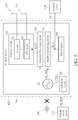
- FIG. 3 is a diagram illustrating a third wireless system according to an embodiment of the present invention.
- the wireless system 300 may be a radar system such as an automotive radar system.
- the wireless system 300 may be a wireless communication system such as a Wi-Fi system.
- the wireless system 300 is implemented on a chip 301, and therefore has a plurality of on-chip components.
- the major difference between the wireless systems 100 and 300 is that the wireless system 300 further includes a frequency processing circuit 302, and the first clock CK_1 is not output to the external device 136.
- the frequency processing circuit 302 is arranged to receive the reference clock CK_REF with the reference frequency different from a second frequency (which may be different from the first frequency of the first clock CK_1), generate a second clock CK_2 with the second frequency according to the reference clock CK_REF, and output the second clock CK_2 to the external device 136 via the interface 138.
- the frequency processing circuit 302 may include a PLL circuit, a frequency multiplier circuit, and/or a frequency divider circuit, depending upon the discrepancy between the second frequency of the second clock CK_2 and the reference frequency of the reference clock CK_REF.
- FIG. 4 is a diagram illustrating a fourth wireless system according to an embodiment of the present invention.
- the wireless system 400 may be a radar system such as an automotive radar system.
- the wireless system 400 may be a wireless communication system such as a Wi-Fi system.
- the wireless system 400 is implemented on a chip 401, and therefore has a plurality of on-chip components.
- the major difference between the wireless systems 300 and 400 is that the wireless system 400 has a direct path 403 connected between an output port of the active oscillator 102 and an input port of the front-end circuit 104.
- the reference clock CK_REF with a reference frequency equal to an LO frequency is supplied to the front-end circuit 104 via the direct path 403, such that the reference clock CK_REF received by the front-end circuit 104 acts as the LO signal S_LO directly.
- the frequency processing circuit 110 used in the wireless system 100/300 may be modified to generate a range of frequencies according to the reference frequency of the reference clock CK_REF and then select one frequency from the range of frequencies as the LO frequency. Selecting an accurate frequency from the range of frequencies can compensate for the drift of the reference frequency, either before or after the frequency calibration of the active oscillator 102. In this way, the frequency regulation can be met.
- FIG. 5 is a diagram illustrating a fifth wireless system according to an embodiment of the present invention.
- the wireless system 500 may be a radar system such as an automotive radar system.
- the wireless system 500 may be a wireless communication system such as a Wi-Fi system.
- the wireless system 500 is implemented on a chip 501, and therefore has a plurality of on-chip components.
- the major difference between the wireless systems 100 and 500 is that the wireless system 500 has a calibration circuit 508 that is arranged to receive an external reference clock CK_EXT from an external source device 502 located outside of the chip 501 and apply frequency calibration to the active oscillator 102 according to the external reference clock CK_EXT.
- FIG. 8 is a diagram illustrating an eighth wireless system according to an embodiment of the present invention.
- the wireless system 800 may be a radar system such as an automotive radar system.
- the wireless system 800 may be a wireless communication system such as a Wi-Fi system.
- the wireless system 800 is implemented on a chip 801, and therefore has a plurality of on-chip components.
- the major difference between the wireless systems 400 and 800 is that the wireless system 800 has the calibration circuit 508 that is arranged to receive the external reference clock CK_EXT from the external source device 502 located outside of the chip 801 and apply frequency calibration to the active oscillator 102 according to the external reference clock CK_EXT.
- the external source device 502 may be an electronic control unit (ECU).
- the calibration circuit 508 may receive an ECU reference clock from a defined interface, and may apply frequency calibration to the active oscillator 102 according to the ECU reference clock, where the frequency calibration may be real-time calibration or power-on calibration. In this way, clock alignment with the external ECU located outside of the chip 501/601/701/801 can be achieved.
- the external reference clock CK_EXT needed by frequency calibration of the active oscillator 102 may be extracted from a radio-frequency (RF) signal and then supplied by the external source device 502.
- RF radio-frequency
- the calibration circuit 508 may be an optional component. Hence, the calibration circuit 508 may be omitted in some embodiments of the present invention.
- any wireless system e.g., wireless system chip
- an active oscillator e.g., on-chip active oscillator
Landscapes
- Engineering & Computer Science (AREA)
- Computer Networks & Wireless Communication (AREA)
- Physics & Mathematics (AREA)
- Radar, Positioning & Navigation (AREA)
- Remote Sensing (AREA)
- Signal Processing (AREA)
- General Physics & Mathematics (AREA)
- Nonlinear Science (AREA)
- Transceivers (AREA)
- Radar Systems Or Details Thereof (AREA)
- Stabilization Of Oscillater, Synchronisation, Frequency Synthesizers (AREA)
Abstract
Description
- This application claims the benefit of
U.S. provisional application No. 62/613,441 filed 01/04/2018 andU.S. provisional application No. 62/655,325 filed 04/10/2018 . The entire contents of the related applications, includingU.S. provisional application No. 62/613,441 U.S. provisional application No. 62/655,325 - The present invention relates to wireless communications, and more particularly, to a wireless system that uses a local oscillator signal derived from a reference clock output of an active oscillator that has no electromechanical resonator (e.g., crystal).
- A transmit (TX) circuit in a wireless system chip is used to perform an up-conversion process that converts a TX signal from a lower frequency to a higher frequency for signal transmission. A receive (RX) circuit in the wireless system chip is used to perform a down-conversion process that converts an RX signal from a higher frequency to a lower frequency for signal reception. Further, each of the up-conversion process and the down-conversion process requires a local oscillator (LO) signal with a proper LO frequency setting. Typically, the LO signal is derived from a reference clock that is supplied from an off-chip oscillator. For example, the off-chip oscillator is a passive oscillator (e.g., a typical crystal oscillator (XO)). When the wireless system chip is used by an application device, the off-chip oscillator is also used by the application device due to the fact that the reference clock needed by the wireless system chip is supplied from the off-chip oscillator (e.g., XO). If the off-chip oscillator can be omitted, the BOM (bill of material) cost and the PCB (printed circuit board) area of the application device can be reduced.
- One of the objectives of the claimed invention is to provide a wireless system that uses a local oscillator signal derived from a reference clock output of an active oscillator that has no electromechanical resonator (e.g., crystal).
- According to a first aspect of the present invention, an exemplary wireless system is disclosed. The exemplary wireless system includes an active oscillator and a front-end circuit. The active oscillator is arranged to generate and output a reference clock. The active oscillator comprises at least one active component, and does not include an electromechanical resonator. The front-end circuit is arranged to process a transmit (TX) signal or a receive (RX) signal according to a local oscillator (LO) signal, wherein the LO signal is derived from the reference clock.
- According to a second aspect of the present invention, an exemplary wireless system implemented on a chip is disclosed. The exemplary wireless system includes an on-chip oscillator and a front-end circuit. The on-chip oscillator is arranged to generate and output a reference clock. The front-end circuit is arranged to process a transmit (TX) signal or a receive (RX) signal according to a local oscillator (LO) signal, wherein the LO signal is derived from the reference clock. The chip is not coupled to an off-chip oscillator when the wireless system is in operation.
- These and other objectives of the present invention will no doubt become obvious to those of ordinary skill in the art after reading the following detailed description of the preferred embodiment that is illustrated in the various figures and drawings.
-
-
FIG. 1 is a diagram illustrating a first wireless system according to an embodiment of the present invention. -
FIG. 2 is a diagram illustrating a second wireless system according to an embodiment of the present invention. -
FIG. 3 is a diagram illustrating a third wireless system according to an embodiment of the present invention. -
FIG. 4 is a diagram illustrating a fourth wireless system according to an embodiment of the present invention. -
FIG. 5 is a diagram illustrating a fifth wireless system according to an embodiment of the present invention. -
FIG. 6 is a diagram illustrating a sixth wireless system according to an embodiment of the present invention. -
FIG. 7 is a diagram illustrating a seventh wireless system according to an embodiment of the present invention. -
FIG. 8 is a diagram illustrating an eighth wireless system according to an embodiment of the present invention. - Certain terms are used throughout the following description and claims, which refer to particular components. As one skilled in the art will appreciate, electronic equipment manufacturers may refer to a component by different names. This document does not intend to distinguish between components that differ in name but not in function. In the following description and in the claims, the terms "include" and "comprise" are used in an open-ended fashion, and thus should be interpreted to mean "include, but not limited to ...". Also, the term "couple" is intended to mean either an indirect or direct electrical connection. Accordingly, if one device is coupled to another device, that connection may be through a direct electrical connection, or through an indirect electrical connection via other devices and connections.
- The present invention proposes a crystal-less (XOless) technique for a wireless system. For example, the XOless technique may be integrated in a wireless system chip. Since an off-chip oscillator such as a crystal oscillator (XO) is not needed by the proposed wireless system chip, a BOM cost of an application device using the proposed wireless system chip can be reduced. Further details of the XOless technique are described with reference to the accompanying drawings.
-
FIG. 1 is a diagram illustrating a first wireless system according to an embodiment of the present invention. For example, thewireless system 100 may be a Radio Detection and Ranging (radar) system. For another example, thewireless system 100 may be a wireless communications system such as a Wi-Fi system. In this embodiment, thewireless system 100 is implemented on achip 101, and therefore has a plurality of on-chip components including anactive oscillator 102, a front-end circuit 104, adigital macro 106, acalibration circuit 108, and a plurality offrequency processing circuits active oscillator 102 includes at least one active component (e.g., transistor(s) and/or amplifier(s)), and does not include an electromechanical resonator such as a crystal, a bulk acoustic wave (BAW) resonator, or a microelectromechanical system (MEMS) resonator. That is, theactive oscillator 102 is an electromechanical-resonator-less oscillator (e.g., a crystal-less oscillator), and does not consist of passive components (e.g., inductor(s), resistor(s), and/or capacitor(s)) only. For example, theactive oscillator 102 may be an LC oscillator having an amplifier circuit and an LC frequency-selective network, where the LC frequency-selective network consists of on-chip passive components only, and is used to create a resonator needed for reference clock generation. For another example, theactive oscillator 102 may be an RC oscillator having an amplifier circuit and an RC frequency-selective network, where the RC frequency-selective network consists of on-chip passive components only, and is used to create a resonator needed for reference clock generation. In this embodiment, theactive oscillator 102 is an on-chip oscillator circuit arranged to generate and output a reference clock CK_REF. - In this embodiment, pin (s) of the
chip 101 are not coupled to an off-chip oscillator 130 when thewireless system 100 is in operation. For example, the off-chip oscillator 130 is a crystal oscillator which uses the mechanical resonance of a vibrating crystal of piezoelectric material to create an electrical signal with a precise frequency. In other words, a normal operation of thewireless system 100 can be achieved with the reference clock CK_REF provided by the on-chip oscillator (i.e., active oscillator 102), and does not require a reference clock supplied from the off-chip oscillator 130 such as a typical crystal oscillator. The off-chip oscillator 130 can be omitted in an application device when the proposedwireless system 100 is used by the application device. In this way, the BOM cost of the application device using the proposedwireless system 100 can be reduced. - The reference clock CK_REF may act as a system clock of the
wireless system 100. Hence, the reference clock CK_REF generated from theactive oscillator 102 can be used to create periodical signals needed by normal operations of other on-chip components, including the front-end circuit 104, thedigital macro 106, etc. - The front-
end circuit 104 is arranged to process a transmit (TX) signal and/or a receive (RX) signal according to a local oscillator (LO) signal S_LO. In this embodiment, the front-end circuit 104 is a transceiver circuit having aTX circuit 122 and anRX circuit 124, where theTX circuit 122 is coupled to an off-chip TX antenna 132, and theRX circuit 134 is coupled to an off-chip RX antenna 134. TheTX circuit 122 is used to perform an up-conversion process that converts the TX signal from a lower frequency to a higher frequency for signal transmission via theTX antenna 132. TheRX circuit 124 is used to receive the RX signal from theRX antenna 134, and perform a down-conversion process that converts the RX signal from a higher frequency to a lower frequency for signal reception. An LO frequency of the LO signal S_LO should be properly set to meet requirements of the up-conversion process and the down-conversion process. For example, the LO frequency may be set by a frequency value at a millimeter wave (mmWave) band, lower than the mmWave band, or higher than the mmWave band, depending upon the actual design considerations . In a case where thewireless system 100 is a radar system (e.g., an automotive radar system), the LO signal S_LO may have the LO frequency at a 3.1-10.6GHz band, 24GHz, 60GHz, a 76-77GHz band, or a 77-81GHz band. However, this is for illustrative purposes only, and is not meant to be a limitation of the present invention. - As shown in
FIG. 1 , onefrequency processing circuit 110 is arranged to receive the reference clock CK_REF with a reference frequency different from the LO frequency, generate the LO signal S_LO with the LO frequency according to the reference clock CK_REF, and output the LO signal S_LO to the front-end circuit 104 (particularly,TX circuit 122 and RX circuit 124). For example, thefrequency processing circuit 110 may include a phase-locked loop (PLL) circuit, a frequency multiplier circuit, and/or a frequency divider circuit, depending upon the discrepancy between the LO frequency of the LO signal S_LO and the reference frequency of the reference clock CK_REF. - The
digital macro 106 is arranged to perform at least one data processing function according to a first clock CK_1 with a first frequency. For example, thedigital macro 106 may have a digital circuit such as an on-chip central processing unit (CPU) or an on-chip radar signal processor (RSP) . As shown inFIG. 1 , anotherfrequency processing circuit 112 is arranged to receive the reference clock CK_REF with the reference frequency different from the first frequency, generate the first clock CK_1 with the first frequency according to the reference clock CK_REF, and output the first clock CK_1 to thedigital macro 106. For example, thefrequency processing circuit 112 may include a PLL circuit, a frequency multiplier circuit, and/or a frequency divider circuit, depending upon the discrepancy between the first frequency of the first clock CK_1 and the reference frequency of the reference clock CK_REF. - Moreover, the first clock CK_1 generated from the
frequency processing circuit 112 may be output to anexternal device 136 that is located outside of thechip 101. Theexternal device 136 is coupled to thechip 101 via aninterface 138 such as a UART (universal asynchronous receiver/transmitter) interface, an OWI (one-wire communication interface), a 3-wire interface, an SPI (serial peripheral interface), an LIN (local interconnect network) bus, or a CAN (controller area network) bus. In other words, the on-chipdigital macro 106 and theexternal device 136 can share the same first clock CK_1 output from thefrequency processing circuit 112. For example, theexternal device 136 may be a digital signal processor (DSP) device or a Flash memory device. - Compared to a reference clock generated from an off-chip crystal oscillator, a reference clock generated from an on-chip active oscillator may have less stability and accuracy. In this embodiment, the
calibration circuit 108 is arranged to control theactive oscillator 102 for calibrating the reference frequency of the reference clock CK_REF. Theactive oscillator 102 changes the reference frequency of the reference clock CK_REF in response to a control signal S_CTRL generated from thecalibration circuit 108. For example, thecalibration circuit 108 is a self-calibration circuit that applies frequency calibration to theactive oscillator 102 in response to frequency drift resulting from temperature variation. - It should be noted that the
calibration circuit 108 may be an optional component. Hence, thecalibration circuit 108 may be omitted in some embodiments of the present invention. In practice, any wireless system (e.g., wireless system chip) using an active oscillator (e.g., on-chip active oscillator) with/without frequency calibration falls within the scope of the present invention. - In the embodiment shown in
FIG. 1 , the reference frequency of the reference clock CK_REF generated from theactive oscillator 102 is different from (e.g., higher than or lower than) the LO frequency needed by the front-end circuit 104. Hence, thefrequency processing circuit 110 is implemented to process the reference clock CK_REF for creating the LO signal S_LO with the needed LO frequency. However, this is for illustrative purposes only, and is not meant to be a limitation of the present invention. In an alternative design, thefrequency processing circuit 110 can be omitted when the reference frequency of the reference clock CK_REF generated from theactive oscillator 102 is equal to the LO frequency needed by the front-end circuit 104. -
FIG. 2 is a diagram illustrating a second wireless system according to an embodiment of the present invention. For example, thewireless system 200 may be a radar system such as an automotive radar system. For another example, thewireless system 200 may be a wireless communication system such as a Wi-Fi system. In this embodiment, thewireless system 200 is implemented on achip 201, and therefore has a plurality of on-chip components. The major difference between thewireless systems wireless system 200 has adirect path 203 connected between an output port of theactive oscillator 102 and an input port of the front-end circuit 104. Hence, the reference clock CK_REF with a reference frequency equal to an LO frequency is supplied to the front-end circuit 104 via thedirect path 203, such that the reference clock CK_REF received by the front-end circuit 104 acts as the LO signal S_LO directly. - In the embodiment shown in
FIG. 1 , the reference frequency of the reference clock CK_REF generated from theactive oscillator 102 is different from (e.g., higher than or lower than) the clock frequency needed by both of thedigital macro 106 and theexternal device 136. Hence, thefrequency processing circuit 112 is implemented to process the reference clock CK_REF for creating the first clock CK_1 with the needed first frequency, where the same first clock CK_1 is shared by the on-chipdigital macro 106 and theexternal device 136. However, this is for illustrative purposes only, and is not meant to be a limitation of the present invention. In an alternative design, the clock frequency needed by thedigital macro 106 and the clock frequency needed by theexternal device 136 are not necessarily the same. When the clock frequency needed by thedigital macro 106 is different from (e.g., higher than or lower than) the clock frequency needed by theexternal device 136, multiple frequency processing circuits may be used in a wireless system. -
FIG. 3 is a diagram illustrating a third wireless system according to an embodiment of the present invention. For example, thewireless system 300 may be a radar system such as an automotive radar system. For another example, thewireless system 300 may be a wireless communication system such as a Wi-Fi system. In this embodiment, thewireless system 300 is implemented on achip 301, and therefore has a plurality of on-chip components. The major difference between thewireless systems wireless system 300 further includes afrequency processing circuit 302, and the first clock CK_1 is not output to theexternal device 136. - The
frequency processing circuit 302 is arranged to receive the reference clock CK_REF with the reference frequency different from a second frequency (which may be different from the first frequency of the first clock CK_1), generate a second clock CK_2 with the second frequency according to the reference clock CK_REF, and output the second clock CK_2 to theexternal device 136 via theinterface 138. For example, thefrequency processing circuit 302 may include a PLL circuit, a frequency multiplier circuit, and/or a frequency divider circuit, depending upon the discrepancy between the second frequency of the second clock CK_2 and the reference frequency of the reference clock CK_REF. - In the embodiment shown in
FIG. 3 , the reference frequency of the reference clock CK_REF generated from theactive oscillator 102 is different from (e.g., higher than or lower than) the LO frequency needed by the front-end circuit 104. Hence, thefrequency processing circuit 110 is implemented to process the reference clock CK_REF for creating the LO signal S_LO with the needed LO frequency. However, this is for illustrative purposes only, and is not meant to be a limitation of the present invention. In an alternative design, thefrequency processing circuit 110 can be omitted when the reference frequency of the reference clock CK_REF generated from theactive oscillator 102 is equal to the LO frequency needed by the front-end circuit 104. -
FIG. 4 is a diagram illustrating a fourth wireless system according to an embodiment of the present invention. For example, thewireless system 400 may be a radar system such as an automotive radar system. For another example, thewireless system 400 may be a wireless communication system such as a Wi-Fi system. In this embodiment, thewireless system 400 is implemented on achip 401, and therefore has a plurality of on-chip components. The major difference between thewireless systems wireless system 400 has adirect path 403 connected between an output port of theactive oscillator 102 and an input port of the front-end circuit 104. Hence, the reference clock CK_REF with a reference frequency equal to an LO frequency is supplied to the front-end circuit 104 via thedirect path 403, such that the reference clock CK_REF received by the front-end circuit 104 acts as the LO signal S_LO directly. - In some embodiments of the present invention, the
frequency processing circuit 110 used in thewireless system 100/300 may be modified to generate a range of frequencies according to the reference frequency of the reference clock CK_REF and then select one frequency from the range of frequencies as the LO frequency. Selecting an accurate frequency from the range of frequencies can compensate for the drift of the reference frequency, either before or after the frequency calibration of theactive oscillator 102. In this way, the frequency regulation can be met. - As mentioned above, the
calibration circuit 108 may be a self-calibration circuit that applies frequency calibration to theactive oscillator 102. However, this is for illustrative purposes only, and is not meant to be a limitation of the present invention. Alternatively, the frequency calibration of theactive oscillator 102 may be based on an external source. -
FIG. 5 is a diagram illustrating a fifth wireless system according to an embodiment of the present invention. For example, thewireless system 500 may be a radar system such as an automotive radar system. For another example, thewireless system 500 may be a wireless communication system such as a Wi-Fi system. In this embodiment, thewireless system 500 is implemented on achip 501, and therefore has a plurality of on-chip components. The major difference between thewireless systems wireless system 500 has acalibration circuit 508 that is arranged to receive an external reference clock CK_EXT from anexternal source device 502 located outside of thechip 501 and apply frequency calibration to theactive oscillator 102 according to the external reference clock CK_EXT. -
FIG. 6 is a diagram illustrating a sixth wireless system according to an embodiment of the present invention. For example, thewireless system 600 may be a radar system such as an automotive radar system. For another example, thewireless system 600 may be a wireless communication system such as a Wi-Fi system. In this embodiment, thewireless system 600 is implemented on achip 601, and therefore has a plurality of on-chip components. The major difference between thewireless systems wireless system 600 has thecalibration circuit 508 that is arranged to receive the external reference clock CK_EXT from theexternal source device 502 located outside of thechip 601 and apply frequency calibration to theactive oscillator 102 according to the external reference clock CK_EXT. -
FIG. 7 is a diagram illustrating a seventh wireless system according to an embodiment of the present invention. For example, thewireless system 700 may be a radar system such as an automotive radar system. For another example, thewireless system 700 may be a wireless communication system such as a Wi-Fi system. In this embodiment, thewireless system 700 is implemented on achip 701, and therefore has a plurality of on-chip components. The major difference between thewireless systems wireless system 700 has thecalibration circuit 508 that is arranged to receive the external reference clock CK_EXT from theexternal source device 502 located outside of thechip 701 and apply frequency calibration to theactive oscillator 102 according to the external reference clock CK_EXT. -
FIG. 8 is a diagram illustrating an eighth wireless system according to an embodiment of the present invention. For example, thewireless system 800 may be a radar system such as an automotive radar system. For another example, thewireless system 800 may be a wireless communication system such as a Wi-Fi system. In this embodiment, thewireless system 800 is implemented on achip 801, and therefore has a plurality of on-chip components. The major difference between thewireless systems wireless system 800 has thecalibration circuit 508 that is arranged to receive the external reference clock CK_EXT from theexternal source device 502 located outside of thechip 801 and apply frequency calibration to theactive oscillator 102 according to the external reference clock CK_EXT. - For example, when the
wireless system 500/600/700/800 is an automotive radar system, theexternal source device 502 may be an electronic control unit (ECU). Hence, thecalibration circuit 508 may receive an ECU reference clock from a defined interface, and may apply frequency calibration to theactive oscillator 102 according to the ECU reference clock, where the frequency calibration may be real-time calibration or power-on calibration. In this way, clock alignment with the external ECU located outside of thechip 501/601/701/801 can be achieved. For another example, the external reference clock CK_EXT needed by frequency calibration of theactive oscillator 102 may be extracted from a radio-frequency (RF) signal and then supplied by theexternal source device 502. - It should be noted that the
calibration circuit 508 may be an optional component. Hence, thecalibration circuit 508 may be omitted in some embodiments of the present invention. In practice, any wireless system (e.g., wireless system chip) using an active oscillator (e.g., on-chip active oscillator) with/without frequency calibration falls within the scope of the present invention. - Those skilled in the art will readily observe that numerous modifications and alterations of the device and method may be made while retaining the teachings of the invention. Accordingly, the above disclosure should be construed as limited only by the metes and bounds of the appended claims.
Claims (15)
- A wireless system (100, 200, 300, 400, 500, 600, 700, 800) comprising:an active oscillator (102), arranged to generate and output a reference clock, wherein the active oscillator (102) comprises at least one active component, and does not include an electromechanical resonator; anda front-end circuit (104), arranged to process a transmit, TX, signal or a receive, RX, signal according to a local oscillator, LO, signal, wherein the LO signal is derived from the reference clock.
- The wireless system (100, 200, 300, 400, 500, 600, 700, 800) of claim 1, wherein the wireless system (100, 200, 300, 400, 500, 600, 700, 800) is a Radio Detection and Ranging, radar, system; or wherein the LO signal has an LO frequency at a 3.1-10.6GHz band, 24GHz, 60GHz, a 76-77GHz band, or a 77-81GHz band; or wherein the wireless system (100, 200, 300, 400, 500, 600, 700, 800) is implemented on a chip, and the active oscillator (102) is an on-chip oscillator; or wherein the reference clock with an LO frequency is supplied to the front-end circuit, and the reference clock received by the front-end circuit acts as the LO signal directly.
- The wireless system (100, 200, 300, 400, 500, 600, 700, 800) of claim 1, further comprising:a frequency processing circuit (110, 112, 302), arranged to receive the reference clock with a reference frequency different from an LO frequency, generate the LO signal with the LO frequency according to the reference clock, and output the LO signal to the front-end circuit.
- The wireless system (100, 200, 300, 400, 500, 600, 700, 800) of claim 1, further comprising:a digital circuit, arranged to perform at least one data processing function according to a clock with a specific frequency; anda frequency processing circuit (110, 112, 302), arranged to receive the reference clock with a reference frequency different from the specific frequency, generate the clock with the specific frequency according to the reference clock, and output the clock to the digital circuit.
- The wireless system (100, 200, 300, 400, 500, 600, 700, 800) of claim 4, wherein the wireless system (100, 200, 300, 400, 500, 600, 700, 800) is implemented on a chip, and the frequency processing circuit (110, 112, 302) is further arranged to output the clock with the specific frequency to an external device that is located outside of the chip.
- The wireless system (100, 200, 300, 400, 500, 600, 700, 800) of claim 1, wherein the wireless system (100, 200, 300, 400, 500, 600, 700, 800) is implemented on a chip, and further comprises:a frequency processing circuit (110, 112, 302), arranged to receive the reference clock with a reference frequency different from a specific frequency, generate a clock with the specific frequency according to the reference clock, and output the clock to an external device that is located outside of the chip.
- The wireless system (100, 200, 300, 400, 500, 600, 700, 800) of claim 1, further comprising:a calibration circuit (108), arranged to control the active oscillator for calibrating a reference frequency of the reference clock.
- The wireless system (100, 200, 300, 400, 500, 600, 700, 800) of claim 7, wherein the wireless system (100, 200, 300, 400, 500, 600, 700, 800) is implemented on a chip, and the calibration circuit (108) is arranged to receive an external reference clock from an external source device located outside of the chip, and calibrate the reference frequency of the reference clock according to the external reference clock.
- A wireless system (100, 200, 300, 400, 500, 600, 700, 800) implemented on a chip, comprising:an on-chip oscillator, arranged to generate and output a reference clock; anda front-end circuit (104), arranged to process a transmit, TX, signal or a receive, RX, signal according to a local oscillator, LO, signal, wherein the LO signal is derived from the reference clock;wherein the chip is not coupled to an off-chip oscillator when the wireless system (100, 200, 300, 400, 500, 600, 700, 800) is in operation.
- The wireless system (100, 200, 300, 400, 500, 600, 700, 800) of claim 9, wherein the on-chip oscillator is an active oscillator having at least one active component, and does not include an electromechanical resonator; or
wherein the wireless system (100, 200, 300, 400, 500, 600, 700, 800) is a Radio Detection and Ranging, radar, system; or
wherein the LO signal has an LO frequency at a 3.1-10.6GHz band, 24GHz, 60GHz, a 76-77GHz band, or a 77-81GHz band; or
wherein the reference clock with an LO frequency is supplied to the front-end circuit, and the reference clock received by the front-end circuit acts as the LO signal directly. - The wireless system (100, 200, 300, 400, 500, 600, 700, 800) of claim 9, further comprising:a frequency processing circuit (110, 112, 302), arranged to receive the reference clock with a reference frequency different from an LO frequency, generate the LO signal with the LO frequency according to the reference clock, and output the LO signal to the front-end circuit; ora frequency processing circuit (110, 112, 302), arranged to receive the reference clock with a reference frequency different from a specific frequency, generate a clock with the specific frequency according to the reference clock, and output the clock to an external device that is located outside of the chip.
- The wireless system (100, 200, 300, 400, 500, 600, 700, 800) of claim 9, further comprising:a digital circuit, arranged to perform at least one data processing function according to a clock with a specific frequency; anda frequency processing circuit (110, 112, 302), arranged to receive the reference clock with a reference frequency different from the specific frequency, generate the clock with the specific frequency according to the reference clock, and output the clock to the digital circuit.
- The wireless system (100, 200, 300, 400, 500, 600, 700, 800) of claim 12, wherein the frequency processing circuit (110, 112, 302) is further arranged to output the clock with the specific frequency to an external device that is located outside of the chip.
- The wireless system (100, 200, 300, 400, 500, 600, 700, 800) of claim 9, further comprising:a calibration circuit (108), arranged to control the on-chip oscillator for calibrating a reference frequency of the reference clock.
- The wireless system (100, 200, 300, 400, 500, 600, 700, 800) of claim 14, wherein the calibration circuit (108)is arranged to receive an external reference clock from an external source device located outside of the chip, and calibrate the reference frequency of the reference clock according to the external reference clock.
Applications Claiming Priority (3)
| Application Number | Priority Date | Filing Date | Title |
|---|---|---|---|
| US201862613441P | 2018-01-04 | 2018-01-04 | |
| US201862655325P | 2018-04-10 | 2018-04-10 | |
| US16/152,391 US11677433B2 (en) | 2018-01-04 | 2018-10-04 | Wireless system having local oscillator signal derived from reference clock output of active oscillator that has no electromechanical resonator |
Publications (3)
| Publication Number | Publication Date |
|---|---|
| EP3509215A2 true EP3509215A2 (en) | 2019-07-10 |
| EP3509215A3 EP3509215A3 (en) | 2019-08-14 |
| EP3509215B1 EP3509215B1 (en) | 2025-07-16 |
Family
ID=64277488
Family Applications (1)
| Application Number | Title | Priority Date | Filing Date |
|---|---|---|---|
| EP18202444.8A Active EP3509215B1 (en) | 2018-01-04 | 2018-10-24 | Wireless system having local oscillator signal derived from reference clock output of active oscillator that has no electromechanical resonator |
Country Status (4)
| Country | Link |
|---|---|
| US (1) | US11677433B2 (en) |
| EP (1) | EP3509215B1 (en) |
| CN (1) | CN110022166A (en) |
| TW (1) | TW201931787A (en) |
Families Citing this family (1)
| Publication number | Priority date | Publication date | Assignee | Title |
|---|---|---|---|---|
| US11221395B2 (en) * | 2019-08-12 | 2022-01-11 | GM Global Technology Operations LLC | Chip-based transmit channel architecture |
Citations (2)
| Publication number | Priority date | Publication date | Assignee | Title |
|---|---|---|---|---|
| EP1807935A1 (en) * | 2004-09-30 | 2007-07-18 | Silicon Laboratories Inc. | Frequency-change rate-limit of capacitor-bank oscillator |
| US20090278617A1 (en) * | 2008-05-12 | 2009-11-12 | National Chiao Tung University | Crystal-less Communications Device and Self-Calibrated Embedded Virtual Crystal Clock Generation Method |
Family Cites Families (17)
| Publication number | Priority date | Publication date | Assignee | Title |
|---|---|---|---|---|
| KR100877253B1 (en) * | 1999-08-02 | 2009-01-07 | 콸콤 인코포레이티드 | Method and apparatus for multiple band voltage controlled oscillator with noise immunity |
| TW586263B (en) | 2003-01-29 | 2004-05-01 | Mediatek Inc | Analog demodulator in a low-IF receiver |
| DE10354521A1 (en) * | 2003-11-14 | 2005-06-23 | Atmel Germany Gmbh | Method for synchronizing several oscillators |
| US7002511B1 (en) | 2005-03-02 | 2006-02-21 | Xytrans, Inc. | Millimeter wave pulsed radar system |
| US7280001B2 (en) * | 2005-09-14 | 2007-10-09 | Silicon Laboratories Inc. | Capacitor array segmentation |
| KR20080051180A (en) | 2005-09-23 | 2008-06-10 | 캘리포니아 인스티튜트 오브 테크놀로지 | A mm-wave fully integrated phased array receiver and transmitter with on chip antennas |
| US7542445B2 (en) * | 2006-06-14 | 2009-06-02 | Sony Ericsson Mobile Communications Ab | Method and system for maintaining autonomous system clock accuracy for a mobile radio terminal |
| WO2009019639A2 (en) | 2007-08-06 | 2009-02-12 | Koninklijke Philips Electronics N.V. | Crystal-less transceivers |
| EP2355380A1 (en) | 2010-01-26 | 2011-08-10 | ST-Ericsson SA | Wireless communication apparatus having modulated Tx clock spur control |
| US8896386B2 (en) | 2012-03-08 | 2014-11-25 | Mediatek Singapore Pte. Ltd. | Calibration device for oscillator and method thereof |
| CN103455085A (en) | 2013-09-16 | 2013-12-18 | 四川和芯微电子股份有限公司 | Circuit and method for generating USB host work clock |
| US8890591B1 (en) | 2013-12-24 | 2014-11-18 | Liming Xiu | Circuit and method of using time-average-frequency direct period syntheszier for improving crystal-less frequency generator frequency stability |
| US9880261B2 (en) | 2014-09-30 | 2018-01-30 | Texas Instruments Incorporated | Loopback techniques for synchronization of oscillator signal in radar |
| US9853648B2 (en) | 2014-10-22 | 2017-12-26 | Mediatek Inc. | Compensation apparatus and inductor-based apparatus |
| TWI523432B (en) | 2014-11-05 | 2016-02-21 | 驊訊電子企業股份有限公司 | Reference frequency calibration module and apparatus using the same |
| US10084438B2 (en) | 2016-03-16 | 2018-09-25 | Mediatek Inc. | Clock generator using passive mixer and associated clock generating method |
| DE102017119212A1 (en) * | 2016-12-20 | 2018-06-21 | Infineon Technologies Ag | RF transceiver with test option |
-
2018
- 2018-10-04 US US16/152,391 patent/US11677433B2/en active Active
- 2018-10-24 EP EP18202444.8A patent/EP3509215B1/en active Active
-
2019
- 2019-01-02 CN CN201910001893.4A patent/CN110022166A/en active Pending
- 2019-01-03 TW TW108100166A patent/TW201931787A/en unknown
Patent Citations (2)
| Publication number | Priority date | Publication date | Assignee | Title |
|---|---|---|---|---|
| EP1807935A1 (en) * | 2004-09-30 | 2007-07-18 | Silicon Laboratories Inc. | Frequency-change rate-limit of capacitor-bank oscillator |
| US20090278617A1 (en) * | 2008-05-12 | 2009-11-12 | National Chiao Tung University | Crystal-less Communications Device and Self-Calibrated Embedded Virtual Crystal Clock Generation Method |
Also Published As
| Publication number | Publication date |
|---|---|
| US11677433B2 (en) | 2023-06-13 |
| US20190207640A1 (en) | 2019-07-04 |
| CN110022166A (en) | 2019-07-16 |
| TW201931787A (en) | 2019-08-01 |
| EP3509215A3 (en) | 2019-08-14 |
| EP3509215B1 (en) | 2025-07-16 |
Similar Documents
| Publication | Publication Date | Title |
|---|---|---|
| US11693089B2 (en) | Apparatus and method for applying frequency calibration to local oscillator signal derived from reference clock output of active oscillator | |
| US20160099700A1 (en) | CMOS Tuner And Related Tuning Algorithm For A Passive Adaptive Antenna Matching Network Suitable For Use With Agile RF Transceivers | |
| EP3502733B1 (en) | Radar system comprising coupling device | |
| US9893716B2 (en) | Resonant circuit calibration | |
| CN102185663B (en) | Frequency calibration method and device | |
| US8412134B2 (en) | Filter circuit, wireless transmitter, and wireless receiver | |
| JP2018023098A (en) | Method and system for conducting high resolution tuning of phase in active load modulation in nfc system | |
| US20240322855A1 (en) | Wireless Circuitry with Loopback Path All-Pass Filters | |
| US20030034852A1 (en) | Oscillation circuit and electronics using the same | |
| EP3761053B1 (en) | Radar sensor, method of operating the radar sensor and program code | |
| EP2336803A1 (en) | Communication device | |
| US11677433B2 (en) | Wireless system having local oscillator signal derived from reference clock output of active oscillator that has no electromechanical resonator | |
| US9531428B2 (en) | Wireless communication calibration system and associated method | |
| CN113300673B (en) | Drift compensation | |
| US11323125B2 (en) | Transceiver circuit and self-calibration method | |
| CN114301453B (en) | Transceiver circuit and self-correction method | |
| US20220268910A1 (en) | Ultra-wideband integrated circuit (uwb ic) and method of calibrating a uwb product that employs the uwb ic | |
| US8872593B2 (en) | On-chip R and C calibration using on-board supply bypass capacitance | |
| JP2002076773A (en) | Temperature compensated oscillator and electronic equipment using the same | |
| CN117278026A (en) | Radio frequency self-calibration method | |
| CN113904679A (en) | transceiver circuit | |
| JP2020052015A (en) | Electronic device and temperature estimation method |
Legal Events
| Date | Code | Title | Description |
|---|---|---|---|
| PUAI | Public reference made under article 153(3) epc to a published international application that has entered the european phase |
Free format text: ORIGINAL CODE: 0009012 |
|
| STAA | Information on the status of an ep patent application or granted ep patent |
Free format text: STATUS: THE APPLICATION HAS BEEN PUBLISHED |
|
| AK | Designated contracting states |
Kind code of ref document: A2 Designated state(s): AL AT BE BG CH CY CZ DE DK EE ES FI FR GB GR HR HU IE IS IT LI LT LU LV MC MK MT NL NO PL PT RO RS SE SI SK SM TR |
|
| AX | Request for extension of the european patent |
Extension state: BA ME |
|
| PUAL | Search report despatched |
Free format text: ORIGINAL CODE: 0009013 |
|
| AK | Designated contracting states |
Kind code of ref document: A3 Designated state(s): AL AT BE BG CH CY CZ DE DK EE ES FI FR GB GR HR HU IE IS IT LI LT LU LV MC MK MT NL NO PL PT RO RS SE SI SK SM TR |
|
| AX | Request for extension of the european patent |
Extension state: BA ME |
|
| RIC1 | Information provided on ipc code assigned before grant |
Ipc: H04B 7/26 20060101ALI20190710BHEP Ipc: H03K 5/135 20060101AFI20190710BHEP |
|
| STAA | Information on the status of an ep patent application or granted ep patent |
Free format text: STATUS: REQUEST FOR EXAMINATION WAS MADE |
|
| 17P | Request for examination filed |
Effective date: 20200120 |
|
| RBV | Designated contracting states (corrected) |
Designated state(s): AL AT BE BG CH CY CZ DE DK EE ES FI FR GB GR HR HU IE IS IT LI LT LU LV MC MK MT NL NO PL PT RO RS SE SI SK SM TR |
|
| STAA | Information on the status of an ep patent application or granted ep patent |
Free format text: STATUS: EXAMINATION IS IN PROGRESS |
|
| 17Q | First examination report despatched |
Effective date: 20200722 |
|
| P01 | Opt-out of the competence of the unified patent court (upc) registered |
Effective date: 20230607 |
|
| GRAP | Despatch of communication of intention to grant a patent |
Free format text: ORIGINAL CODE: EPIDOSNIGR1 |
|
| STAA | Information on the status of an ep patent application or granted ep patent |
Free format text: STATUS: GRANT OF PATENT IS INTENDED |
|
| INTG | Intention to grant announced |
Effective date: 20250214 |
|
| GRAS | Grant fee paid |
Free format text: ORIGINAL CODE: EPIDOSNIGR3 |
|
| GRAA | (expected) grant |
Free format text: ORIGINAL CODE: 0009210 |
|
| STAA | Information on the status of an ep patent application or granted ep patent |
Free format text: STATUS: THE PATENT HAS BEEN GRANTED |
|
| AK | Designated contracting states |
Kind code of ref document: B1 Designated state(s): AL AT BE BG CH CY CZ DE DK EE ES FI FR GB GR HR HU IE IS IT LI LT LU LV MC MK MT NL NO PL PT RO RS SE SI SK SM TR |
|
| REG | Reference to a national code |
Ref country code: GB Ref legal event code: FG4D |
|
| REG | Reference to a national code |
Ref country code: CH Ref legal event code: EP |
|
| REG | Reference to a national code |
Ref country code: DE Ref legal event code: R096 Ref document number: 602018083584 Country of ref document: DE |
|
| REG | Reference to a national code |
Ref country code: IE Ref legal event code: FG4D |
|
| PGFP | Annual fee paid to national office [announced via postgrant information from national office to epo] |
Ref country code: GB Payment date: 20250801 Year of fee payment: 8 |
|
| PGFP | Annual fee paid to national office [announced via postgrant information from national office to epo] |
Ref country code: FR Payment date: 20250730 Year of fee payment: 8 |
|
| REG | Reference to a national code |
Ref country code: NL Ref legal event code: MP Effective date: 20250716 |
|
| PG25 | Lapsed in a contracting state [announced via postgrant information from national office to epo] |
Ref country code: PT Free format text: LAPSE BECAUSE OF FAILURE TO SUBMIT A TRANSLATION OF THE DESCRIPTION OR TO PAY THE FEE WITHIN THE PRESCRIBED TIME-LIMIT Effective date: 20251117 |
|
| PG25 | Lapsed in a contracting state [announced via postgrant information from national office to epo] |
Ref country code: NL Free format text: LAPSE BECAUSE OF FAILURE TO SUBMIT A TRANSLATION OF THE DESCRIPTION OR TO PAY THE FEE WITHIN THE PRESCRIBED TIME-LIMIT Effective date: 20250716 |
|
| REG | Reference to a national code |
Ref country code: AT Ref legal event code: MK05 Ref document number: 1815015 Country of ref document: AT Kind code of ref document: T Effective date: 20250716 |
|
| PG25 | Lapsed in a contracting state [announced via postgrant information from national office to epo] |
Ref country code: IS Free format text: LAPSE BECAUSE OF FAILURE TO SUBMIT A TRANSLATION OF THE DESCRIPTION OR TO PAY THE FEE WITHIN THE PRESCRIBED TIME-LIMIT Effective date: 20251116 |
|
| PGFP | Annual fee paid to national office [announced via postgrant information from national office to epo] |
Ref country code: DE Payment date: 20250714 Year of fee payment: 8 |
|
| PG25 | Lapsed in a contracting state [announced via postgrant information from national office to epo] |
Ref country code: NO Free format text: LAPSE BECAUSE OF FAILURE TO SUBMIT A TRANSLATION OF THE DESCRIPTION OR TO PAY THE FEE WITHIN THE PRESCRIBED TIME-LIMIT Effective date: 20251016 |
|
| REG | Reference to a national code |
Ref country code: LT Ref legal event code: MG9D |
|
| PG25 | Lapsed in a contracting state [announced via postgrant information from national office to epo] |
Ref country code: AT Free format text: LAPSE BECAUSE OF FAILURE TO SUBMIT A TRANSLATION OF THE DESCRIPTION OR TO PAY THE FEE WITHIN THE PRESCRIBED TIME-LIMIT Effective date: 20250716 |
|
| PG25 | Lapsed in a contracting state [announced via postgrant information from national office to epo] |
Ref country code: FI Free format text: LAPSE BECAUSE OF FAILURE TO SUBMIT A TRANSLATION OF THE DESCRIPTION OR TO PAY THE FEE WITHIN THE PRESCRIBED TIME-LIMIT Effective date: 20250716 |
|
| PG25 | Lapsed in a contracting state [announced via postgrant information from national office to epo] |
Ref country code: HR Free format text: LAPSE BECAUSE OF FAILURE TO SUBMIT A TRANSLATION OF THE DESCRIPTION OR TO PAY THE FEE WITHIN THE PRESCRIBED TIME-LIMIT Effective date: 20250716 |
|
| PG25 | Lapsed in a contracting state [announced via postgrant information from national office to epo] |
Ref country code: GR Free format text: LAPSE BECAUSE OF FAILURE TO SUBMIT A TRANSLATION OF THE DESCRIPTION OR TO PAY THE FEE WITHIN THE PRESCRIBED TIME-LIMIT Effective date: 20251017 |
|
| PG25 | Lapsed in a contracting state [announced via postgrant information from national office to epo] |
Ref country code: SE Free format text: LAPSE BECAUSE OF FAILURE TO SUBMIT A TRANSLATION OF THE DESCRIPTION OR TO PAY THE FEE WITHIN THE PRESCRIBED TIME-LIMIT Effective date: 20250716 |
|
| PG25 | Lapsed in a contracting state [announced via postgrant information from national office to epo] |
Ref country code: LV Free format text: LAPSE BECAUSE OF FAILURE TO SUBMIT A TRANSLATION OF THE DESCRIPTION OR TO PAY THE FEE WITHIN THE PRESCRIBED TIME-LIMIT Effective date: 20250716 |
|
| PG25 | Lapsed in a contracting state [announced via postgrant information from national office to epo] |
Ref country code: BG Free format text: LAPSE BECAUSE OF FAILURE TO SUBMIT A TRANSLATION OF THE DESCRIPTION OR TO PAY THE FEE WITHIN THE PRESCRIBED TIME-LIMIT Effective date: 20250716 Ref country code: PL Free format text: LAPSE BECAUSE OF FAILURE TO SUBMIT A TRANSLATION OF THE DESCRIPTION OR TO PAY THE FEE WITHIN THE PRESCRIBED TIME-LIMIT Effective date: 20250716 |
|
| PG25 | Lapsed in a contracting state [announced via postgrant information from national office to epo] |
Ref country code: RS Free format text: LAPSE BECAUSE OF FAILURE TO SUBMIT A TRANSLATION OF THE DESCRIPTION OR TO PAY THE FEE WITHIN THE PRESCRIBED TIME-LIMIT Effective date: 20251016 |
|
| PG25 | Lapsed in a contracting state [announced via postgrant information from national office to epo] |
Ref country code: ES Free format text: LAPSE BECAUSE OF FAILURE TO SUBMIT A TRANSLATION OF THE DESCRIPTION OR TO PAY THE FEE WITHIN THE PRESCRIBED TIME-LIMIT Effective date: 20250716 |
|
| PG25 | Lapsed in a contracting state [announced via postgrant information from national office to epo] |
Ref country code: RO Free format text: LAPSE BECAUSE OF FAILURE TO SUBMIT A TRANSLATION OF THE DESCRIPTION OR TO PAY THE FEE WITHIN THE PRESCRIBED TIME-LIMIT Effective date: 20250716 |
|
| PG25 | Lapsed in a contracting state [announced via postgrant information from national office to epo] |
Ref country code: SM Free format text: LAPSE BECAUSE OF FAILURE TO SUBMIT A TRANSLATION OF THE DESCRIPTION OR TO PAY THE FEE WITHIN THE PRESCRIBED TIME-LIMIT Effective date: 20250716 |
|
| PG25 | Lapsed in a contracting state [announced via postgrant information from national office to epo] |
Ref country code: DK Free format text: LAPSE BECAUSE OF FAILURE TO SUBMIT A TRANSLATION OF THE DESCRIPTION OR TO PAY THE FEE WITHIN THE PRESCRIBED TIME-LIMIT Effective date: 20250716 |
|
| PG25 | Lapsed in a contracting state [announced via postgrant information from national office to epo] |
Ref country code: IT Free format text: LAPSE BECAUSE OF FAILURE TO SUBMIT A TRANSLATION OF THE DESCRIPTION OR TO PAY THE FEE WITHIN THE PRESCRIBED TIME-LIMIT Effective date: 20250716 |
|
| PG25 | Lapsed in a contracting state [announced via postgrant information from national office to epo] |
Ref country code: CZ Free format text: LAPSE BECAUSE OF FAILURE TO SUBMIT A TRANSLATION OF THE DESCRIPTION OR TO PAY THE FEE WITHIN THE PRESCRIBED TIME-LIMIT Effective date: 20250716 |
|
| PG25 | Lapsed in a contracting state [announced via postgrant information from national office to epo] |
Ref country code: SK Free format text: LAPSE BECAUSE OF FAILURE TO SUBMIT A TRANSLATION OF THE DESCRIPTION OR TO PAY THE FEE WITHIN THE PRESCRIBED TIME-LIMIT Effective date: 20250716 Ref country code: EE Free format text: LAPSE BECAUSE OF FAILURE TO SUBMIT A TRANSLATION OF THE DESCRIPTION OR TO PAY THE FEE WITHIN THE PRESCRIBED TIME-LIMIT Effective date: 20250716 |