EP3509125A1 - Hermetic thin film electrochemical cells housed in a ceramic casing and activated with a solid electrolyte - Google Patents
Hermetic thin film electrochemical cells housed in a ceramic casing and activated with a solid electrolyte Download PDFInfo
- Publication number
- EP3509125A1 EP3509125A1 EP19150718.5A EP19150718A EP3509125A1 EP 3509125 A1 EP3509125 A1 EP 3509125A1 EP 19150718 A EP19150718 A EP 19150718A EP 3509125 A1 EP3509125 A1 EP 3509125A1
- Authority
- EP
- European Patent Office
- Prior art keywords
- substrate
- current collector
- electrochemical cell
- ceramic
- electrode
- Prior art date
- Legal status (The legal status is an assumption and is not a legal conclusion. Google has not performed a legal analysis and makes no representation as to the accuracy of the status listed.)
- Granted
Links
- 239000000919 ceramic Substances 0.000 title claims abstract description 96
- 239000007784 solid electrolyte Substances 0.000 title claims abstract description 25
- 239000010409 thin film Substances 0.000 title abstract description 10
- 238000001465 metallisation Methods 0.000 claims abstract description 50
- PCHJSUWPFVWCPO-UHFFFAOYSA-N gold Chemical compound [Au] PCHJSUWPFVWCPO-UHFFFAOYSA-N 0.000 claims abstract description 34
- 229910052737 gold Inorganic materials 0.000 claims abstract description 34
- 239000010931 gold Substances 0.000 claims abstract description 34
- RTAQQCXQSZGOHL-UHFFFAOYSA-N Titanium Chemical compound [Ti] RTAQQCXQSZGOHL-UHFFFAOYSA-N 0.000 claims abstract description 14
- 239000010936 titanium Substances 0.000 claims abstract description 14
- 229910052719 titanium Inorganic materials 0.000 claims abstract description 14
- 229910014892 LixPOyNz Inorganic materials 0.000 claims abstract description 6
- 239000000758 substrate Substances 0.000 claims description 147
- 230000002093 peripheral effect Effects 0.000 claims description 31
- 229910052594 sapphire Inorganic materials 0.000 claims description 22
- 239000010980 sapphire Substances 0.000 claims description 21
- 239000006182 cathode active material Substances 0.000 claims description 17
- PNEYBMLMFCGWSK-UHFFFAOYSA-N aluminium oxide Inorganic materials [O-2].[O-2].[O-2].[Al+3].[Al+3] PNEYBMLMFCGWSK-UHFFFAOYSA-N 0.000 claims description 14
- 239000007772 electrode material Substances 0.000 claims description 14
- 239000006183 anode active material Substances 0.000 claims description 11
- PXHVJJICTQNCMI-UHFFFAOYSA-N Nickel Chemical compound [Ni] PXHVJJICTQNCMI-UHFFFAOYSA-N 0.000 claims description 10
- BASFCYQUMIYNBI-UHFFFAOYSA-N platinum Chemical compound [Pt] BASFCYQUMIYNBI-UHFFFAOYSA-N 0.000 claims description 8
- WHXSMMKQMYFTQS-UHFFFAOYSA-N Lithium Chemical compound [Li] WHXSMMKQMYFTQS-UHFFFAOYSA-N 0.000 claims description 6
- 229910045601 alloy Inorganic materials 0.000 claims description 6
- 239000000956 alloy Substances 0.000 claims description 6
- 229910052744 lithium Inorganic materials 0.000 claims description 6
- 239000010955 niobium Substances 0.000 claims description 6
- 229910052758 niobium Inorganic materials 0.000 claims description 6
- GUCVJGMIXFAOAE-UHFFFAOYSA-N niobium atom Chemical compound [Nb] GUCVJGMIXFAOAE-UHFFFAOYSA-N 0.000 claims description 6
- RYGMFSIKBFXOCR-UHFFFAOYSA-N Copper Chemical compound [Cu] RYGMFSIKBFXOCR-UHFFFAOYSA-N 0.000 claims description 5
- 229910052802 copper Inorganic materials 0.000 claims description 5
- 239000010949 copper Substances 0.000 claims description 5
- 239000003792 electrolyte Substances 0.000 claims description 5
- 230000003746 surface roughness Effects 0.000 claims description 5
- GNTDGMZSJNCJKK-UHFFFAOYSA-N divanadium pentaoxide Chemical compound O=[V](=O)O[V](=O)=O GNTDGMZSJNCJKK-UHFFFAOYSA-N 0.000 claims description 4
- 229910052759 nickel Inorganic materials 0.000 claims description 4
- 229910052697 platinum Inorganic materials 0.000 claims description 4
- 238000007789 sealing Methods 0.000 claims description 4
- 229910032387 LiCoO2 Inorganic materials 0.000 claims description 3
- ZOKXTWBITQBERF-UHFFFAOYSA-N Molybdenum Chemical compound [Mo] ZOKXTWBITQBERF-UHFFFAOYSA-N 0.000 claims description 3
- 229910017052 cobalt Inorganic materials 0.000 claims description 3
- 239000010941 cobalt Substances 0.000 claims description 3
- GUTLYIVDDKVIGB-UHFFFAOYSA-N cobalt atom Chemical compound [Co] GUTLYIVDDKVIGB-UHFFFAOYSA-N 0.000 claims description 3
- 229910052750 molybdenum Inorganic materials 0.000 claims description 3
- 239000011733 molybdenum Substances 0.000 claims description 3
- 229910001220 stainless steel Inorganic materials 0.000 claims description 3
- 239000010935 stainless steel Substances 0.000 claims description 3
- 229910052715 tantalum Inorganic materials 0.000 claims description 3
- GUVRBAGPIYLISA-UHFFFAOYSA-N tantalum atom Chemical compound [Ta] GUVRBAGPIYLISA-UHFFFAOYSA-N 0.000 claims description 3
- 229910017656 Ag2V4O11 Inorganic materials 0.000 claims description 2
- 229910007857 Li-Al Inorganic materials 0.000 claims description 2
- -1 Li-Si Inorganic materials 0.000 claims description 2
- 229910008365 Li-Sn Inorganic materials 0.000 claims description 2
- 229910052493 LiFePO4 Inorganic materials 0.000 claims description 2
- 229910002993 LiMnO2 Inorganic materials 0.000 claims description 2
- 229910002097 Lithium manganese(III,IV) oxide Inorganic materials 0.000 claims description 2
- 229910008447 Li—Al Inorganic materials 0.000 claims description 2
- 229910008290 Li—B Inorganic materials 0.000 claims description 2
- 229910006742 Li—Si—B Inorganic materials 0.000 claims description 2
- 229910006759 Li—Sn Inorganic materials 0.000 claims description 2
- 229910052782 aluminium Inorganic materials 0.000 claims description 2
- XAGFODPZIPBFFR-UHFFFAOYSA-N aluminium Chemical compound [Al] XAGFODPZIPBFFR-UHFFFAOYSA-N 0.000 claims description 2
- 239000000203 mixture Substances 0.000 claims description 2
- 239000010410 layer Substances 0.000 abstract description 26
- 239000011229 interlayer Substances 0.000 abstract description 5
- 229910052751 metal Inorganic materials 0.000 abstract description 5
- 239000002184 metal Substances 0.000 abstract description 5
- 238000005219 brazing Methods 0.000 abstract description 4
- 238000005304 joining Methods 0.000 abstract description 2
- 210000004027 cell Anatomy 0.000 description 74
- 239000013078 crystal Substances 0.000 description 5
- 239000000463 material Substances 0.000 description 5
- 238000004519 manufacturing process Methods 0.000 description 4
- 238000000576 coating method Methods 0.000 description 3
- 229910052593 corundum Inorganic materials 0.000 description 3
- 239000010431 corundum Substances 0.000 description 3
- 230000001351 cycling effect Effects 0.000 description 3
- 229910003460 diamond Inorganic materials 0.000 description 3
- 239000010432 diamond Substances 0.000 description 3
- 238000007599 discharging Methods 0.000 description 3
- 238000005538 encapsulation Methods 0.000 description 3
- 239000007769 metal material Substances 0.000 description 3
- 238000000034 method Methods 0.000 description 3
- 238000003466 welding Methods 0.000 description 3
- XEEYBQQBJWHFJM-UHFFFAOYSA-N Iron Chemical compound [Fe] XEEYBQQBJWHFJM-UHFFFAOYSA-N 0.000 description 2
- 239000012790 adhesive layer Substances 0.000 description 2
- 238000013459 approach Methods 0.000 description 2
- 238000003491 array Methods 0.000 description 2
- 239000011248 coating agent Substances 0.000 description 2
- 239000003086 colorant Substances 0.000 description 2
- 238000005516 engineering process Methods 0.000 description 2
- 238000011049 filling Methods 0.000 description 2
- 238000000227 grinding Methods 0.000 description 2
- 229910052500 inorganic mineral Inorganic materials 0.000 description 2
- 239000011707 mineral Substances 0.000 description 2
- 238000005240 physical vapour deposition Methods 0.000 description 2
- 238000005498 polishing Methods 0.000 description 2
- 239000002002 slurry Substances 0.000 description 2
- 239000000126 substance Substances 0.000 description 2
- OKTJSMMVPCPJKN-UHFFFAOYSA-N Carbon Chemical compound [C] OKTJSMMVPCPJKN-UHFFFAOYSA-N 0.000 description 1
- VYZAMTAEIAYCRO-UHFFFAOYSA-N Chromium Chemical compound [Cr] VYZAMTAEIAYCRO-UHFFFAOYSA-N 0.000 description 1
- 229910002986 Li4Ti5O12 Inorganic materials 0.000 description 1
- HBBGRARXTFLTSG-UHFFFAOYSA-N Lithium ion Chemical compound [Li+] HBBGRARXTFLTSG-UHFFFAOYSA-N 0.000 description 1
- FYYHWMGAXLPEAU-UHFFFAOYSA-N Magnesium Chemical compound [Mg] FYYHWMGAXLPEAU-UHFFFAOYSA-N 0.000 description 1
- 238000000137 annealing Methods 0.000 description 1
- 230000015572 biosynthetic process Effects 0.000 description 1
- 229910052793 cadmium Inorganic materials 0.000 description 1
- 229910052799 carbon Inorganic materials 0.000 description 1
- 229910010293 ceramic material Inorganic materials 0.000 description 1
- 238000006243 chemical reaction Methods 0.000 description 1
- 229910052804 chromium Inorganic materials 0.000 description 1
- 239000011651 chromium Substances 0.000 description 1
- 238000010276 construction Methods 0.000 description 1
- 239000000356 contaminant Substances 0.000 description 1
- 230000008602 contraction Effects 0.000 description 1
- 230000007797 corrosion Effects 0.000 description 1
- 238000005260 corrosion Methods 0.000 description 1
- 230000007547 defect Effects 0.000 description 1
- 230000002950 deficient Effects 0.000 description 1
- 210000001787 dendrite Anatomy 0.000 description 1
- 238000000151 deposition Methods 0.000 description 1
- 230000008021 deposition Effects 0.000 description 1
- 238000009792 diffusion process Methods 0.000 description 1
- 238000003487 electrochemical reaction Methods 0.000 description 1
- 238000010348 incorporation Methods 0.000 description 1
- 229910000765 intermetallic Inorganic materials 0.000 description 1
- 229910052742 iron Inorganic materials 0.000 description 1
- 238000002955 isolation Methods 0.000 description 1
- 229910001416 lithium ion Inorganic materials 0.000 description 1
- 229910021450 lithium metal oxide Inorganic materials 0.000 description 1
- VGYDTVNNDKLMHX-UHFFFAOYSA-N lithium;manganese;nickel;oxocobalt Chemical compound [Li].[Mn].[Ni].[Co]=O VGYDTVNNDKLMHX-UHFFFAOYSA-N 0.000 description 1
- 229910052749 magnesium Inorganic materials 0.000 description 1
- 239000011777 magnesium Substances 0.000 description 1
- 239000011572 manganese Substances 0.000 description 1
- 229910052987 metal hydride Inorganic materials 0.000 description 1
- 229910044991 metal oxide Inorganic materials 0.000 description 1
- 150000004706 metal oxides Chemical class 0.000 description 1
- 238000012986 modification Methods 0.000 description 1
- 230000004048 modification Effects 0.000 description 1
- 229910003465 moissanite Inorganic materials 0.000 description 1
- 238000012545 processing Methods 0.000 description 1
- 239000010979 ruby Substances 0.000 description 1
- 229910001750 ruby Inorganic materials 0.000 description 1
- 238000002560 therapeutic procedure Methods 0.000 description 1
- XLYOFNOQVPJJNP-UHFFFAOYSA-N water Substances O XLYOFNOQVPJJNP-UHFFFAOYSA-N 0.000 description 1
Images


Classifications
-
- H—ELECTRICITY
- H01—ELECTRIC ELEMENTS
- H01M—PROCESSES OR MEANS, e.g. BATTERIES, FOR THE DIRECT CONVERSION OF CHEMICAL ENERGY INTO ELECTRICAL ENERGY
- H01M50/00—Constructional details or processes of manufacture of the non-active parts of electrochemical cells other than fuel cells, e.g. hybrid cells
- H01M50/10—Primary casings; Jackets or wrappings
- H01M50/147—Lids or covers
- H01M50/166—Lids or covers characterised by the methods of assembling casings with lids
- H01M50/169—Lids or covers characterised by the methods of assembling casings with lids by welding, brazing or soldering
-
- H—ELECTRICITY
- H01—ELECTRIC ELEMENTS
- H01M—PROCESSES OR MEANS, e.g. BATTERIES, FOR THE DIRECT CONVERSION OF CHEMICAL ENERGY INTO ELECTRICAL ENERGY
- H01M50/00—Constructional details or processes of manufacture of the non-active parts of electrochemical cells other than fuel cells, e.g. hybrid cells
- H01M50/10—Primary casings; Jackets or wrappings
-
- H—ELECTRICITY
- H01—ELECTRIC ELEMENTS
- H01M—PROCESSES OR MEANS, e.g. BATTERIES, FOR THE DIRECT CONVERSION OF CHEMICAL ENERGY INTO ELECTRICAL ENERGY
- H01M10/00—Secondary cells; Manufacture thereof
- H01M10/05—Accumulators with non-aqueous electrolyte
- H01M10/052—Li-accumulators
- H01M10/0525—Rocking-chair batteries, i.e. batteries with lithium insertion or intercalation in both electrodes; Lithium-ion batteries
-
- H—ELECTRICITY
- H01—ELECTRIC ELEMENTS
- H01M—PROCESSES OR MEANS, e.g. BATTERIES, FOR THE DIRECT CONVERSION OF CHEMICAL ENERGY INTO ELECTRICAL ENERGY
- H01M4/00—Electrodes
- H01M4/02—Electrodes composed of, or comprising, active material
- H01M4/13—Electrodes for accumulators with non-aqueous electrolyte, e.g. for lithium-accumulators; Processes of manufacture thereof
- H01M4/131—Electrodes based on mixed oxides or hydroxides, or on mixtures of oxides or hydroxides, e.g. LiCoOx
-
- H—ELECTRICITY
- H01—ELECTRIC ELEMENTS
- H01M—PROCESSES OR MEANS, e.g. BATTERIES, FOR THE DIRECT CONVERSION OF CHEMICAL ENERGY INTO ELECTRICAL ENERGY
- H01M50/00—Constructional details or processes of manufacture of the non-active parts of electrochemical cells other than fuel cells, e.g. hybrid cells
- H01M50/10—Primary casings; Jackets or wrappings
- H01M50/116—Primary casings; Jackets or wrappings characterised by the material
-
- H—ELECTRICITY
- H01—ELECTRIC ELEMENTS
- H01M—PROCESSES OR MEANS, e.g. BATTERIES, FOR THE DIRECT CONVERSION OF CHEMICAL ENERGY INTO ELECTRICAL ENERGY
- H01M50/00—Constructional details or processes of manufacture of the non-active parts of electrochemical cells other than fuel cells, e.g. hybrid cells
- H01M50/10—Primary casings; Jackets or wrappings
- H01M50/116—Primary casings; Jackets or wrappings characterised by the material
- H01M50/117—Inorganic material
-
- H—ELECTRICITY
- H01—ELECTRIC ELEMENTS
- H01M—PROCESSES OR MEANS, e.g. BATTERIES, FOR THE DIRECT CONVERSION OF CHEMICAL ENERGY INTO ELECTRICAL ENERGY
- H01M50/00—Constructional details or processes of manufacture of the non-active parts of electrochemical cells other than fuel cells, e.g. hybrid cells
- H01M50/10—Primary casings; Jackets or wrappings
- H01M50/147—Lids or covers
-
- H—ELECTRICITY
- H01—ELECTRIC ELEMENTS
- H01M—PROCESSES OR MEANS, e.g. BATTERIES, FOR THE DIRECT CONVERSION OF CHEMICAL ENERGY INTO ELECTRICAL ENERGY
- H01M50/00—Constructional details or processes of manufacture of the non-active parts of electrochemical cells other than fuel cells, e.g. hybrid cells
- H01M50/10—Primary casings; Jackets or wrappings
- H01M50/147—Lids or covers
- H01M50/155—Lids or covers characterised by the material
-
- H—ELECTRICITY
- H01—ELECTRIC ELEMENTS
- H01M—PROCESSES OR MEANS, e.g. BATTERIES, FOR THE DIRECT CONVERSION OF CHEMICAL ENERGY INTO ELECTRICAL ENERGY
- H01M50/00—Constructional details or processes of manufacture of the non-active parts of electrochemical cells other than fuel cells, e.g. hybrid cells
- H01M50/10—Primary casings; Jackets or wrappings
- H01M50/183—Sealing members
- H01M50/186—Sealing members characterised by the disposition of the sealing members
-
- H—ELECTRICITY
- H01—ELECTRIC ELEMENTS
- H01M—PROCESSES OR MEANS, e.g. BATTERIES, FOR THE DIRECT CONVERSION OF CHEMICAL ENERGY INTO ELECTRICAL ENERGY
- H01M50/00—Constructional details or processes of manufacture of the non-active parts of electrochemical cells other than fuel cells, e.g. hybrid cells
- H01M50/10—Primary casings; Jackets or wrappings
- H01M50/183—Sealing members
- H01M50/19—Sealing members characterised by the material
- H01M50/191—Inorganic material
-
- H—ELECTRICITY
- H01—ELECTRIC ELEMENTS
- H01M—PROCESSES OR MEANS, e.g. BATTERIES, FOR THE DIRECT CONVERSION OF CHEMICAL ENERGY INTO ELECTRICAL ENERGY
- H01M50/00—Constructional details or processes of manufacture of the non-active parts of electrochemical cells other than fuel cells, e.g. hybrid cells
- H01M50/50—Current conducting connections for cells or batteries
- H01M50/543—Terminals
-
- H—ELECTRICITY
- H01—ELECTRIC ELEMENTS
- H01M—PROCESSES OR MEANS, e.g. BATTERIES, FOR THE DIRECT CONVERSION OF CHEMICAL ENERGY INTO ELECTRICAL ENERGY
- H01M50/00—Constructional details or processes of manufacture of the non-active parts of electrochemical cells other than fuel cells, e.g. hybrid cells
- H01M50/10—Primary casings; Jackets or wrappings
- H01M50/102—Primary casings; Jackets or wrappings characterised by their shape or physical structure
- H01M50/103—Primary casings; Jackets or wrappings characterised by their shape or physical structure prismatic or rectangular
-
- H—ELECTRICITY
- H01—ELECTRIC ELEMENTS
- H01M—PROCESSES OR MEANS, e.g. BATTERIES, FOR THE DIRECT CONVERSION OF CHEMICAL ENERGY INTO ELECTRICAL ENERGY
- H01M50/00—Constructional details or processes of manufacture of the non-active parts of electrochemical cells other than fuel cells, e.g. hybrid cells
- H01M50/10—Primary casings; Jackets or wrappings
- H01M50/116—Primary casings; Jackets or wrappings characterised by the material
- H01M50/117—Inorganic material
- H01M50/119—Metals
-
- H—ELECTRICITY
- H01—ELECTRIC ELEMENTS
- H01M—PROCESSES OR MEANS, e.g. BATTERIES, FOR THE DIRECT CONVERSION OF CHEMICAL ENERGY INTO ELECTRICAL ENERGY
- H01M50/00—Constructional details or processes of manufacture of the non-active parts of electrochemical cells other than fuel cells, e.g. hybrid cells
- H01M50/10—Primary casings; Jackets or wrappings
- H01M50/116—Primary casings; Jackets or wrappings characterised by the material
- H01M50/124—Primary casings; Jackets or wrappings characterised by the material having a layered structure
-
- H—ELECTRICITY
- H01—ELECTRIC ELEMENTS
- H01M—PROCESSES OR MEANS, e.g. BATTERIES, FOR THE DIRECT CONVERSION OF CHEMICAL ENERGY INTO ELECTRICAL ENERGY
- H01M50/00—Constructional details or processes of manufacture of the non-active parts of electrochemical cells other than fuel cells, e.g. hybrid cells
- H01M50/10—Primary casings; Jackets or wrappings
- H01M50/147—Lids or covers
- H01M50/155—Lids or covers characterised by the material
- H01M50/157—Inorganic material
-
- H—ELECTRICITY
- H01—ELECTRIC ELEMENTS
- H01M—PROCESSES OR MEANS, e.g. BATTERIES, FOR THE DIRECT CONVERSION OF CHEMICAL ENERGY INTO ELECTRICAL ENERGY
- H01M50/00—Constructional details or processes of manufacture of the non-active parts of electrochemical cells other than fuel cells, e.g. hybrid cells
- H01M50/50—Current conducting connections for cells or batteries
- H01M50/543—Terminals
- H01M50/547—Terminals characterised by the disposition of the terminals on the cells
- H01M50/55—Terminals characterised by the disposition of the terminals on the cells on the same side of the cell
-
- H—ELECTRICITY
- H01—ELECTRIC ELEMENTS
- H01M—PROCESSES OR MEANS, e.g. BATTERIES, FOR THE DIRECT CONVERSION OF CHEMICAL ENERGY INTO ELECTRICAL ENERGY
- H01M50/00—Constructional details or processes of manufacture of the non-active parts of electrochemical cells other than fuel cells, e.g. hybrid cells
- H01M50/50—Current conducting connections for cells or batteries
- H01M50/543—Terminals
- H01M50/562—Terminals characterised by the material
-
- Y—GENERAL TAGGING OF NEW TECHNOLOGICAL DEVELOPMENTS; GENERAL TAGGING OF CROSS-SECTIONAL TECHNOLOGIES SPANNING OVER SEVERAL SECTIONS OF THE IPC; TECHNICAL SUBJECTS COVERED BY FORMER USPC CROSS-REFERENCE ART COLLECTIONS [XRACs] AND DIGESTS
- Y02—TECHNOLOGIES OR APPLICATIONS FOR MITIGATION OR ADAPTATION AGAINST CLIMATE CHANGE
- Y02E—REDUCTION OF GREENHOUSE GAS [GHG] EMISSIONS, RELATED TO ENERGY GENERATION, TRANSMISSION OR DISTRIBUTION
- Y02E60/00—Enabling technologies; Technologies with a potential or indirect contribution to GHG emissions mitigation
- Y02E60/10—Energy storage using batteries
Definitions
- Electrochemical cells must have two opposite polarity terminals that are electrically isolated from each other. In use, the terminals are connected to a load, such as the circuitry in an implantable medical device to power the medical device. In that respect, an electrochemical cell which is sufficiently hermetic to prevent ingress of moisture and egress of electrolyte so that it can operate for 10 years or more requires robust sealing methodologies while still providing adequate electrical isolation between the opposite polarity terminals.
- convention sealing techniques are often not practical when cell size drops below 0.5 cc. That is because the seals themselves take up a major portion of the overall cell volume.
Landscapes
- Chemical & Material Sciences (AREA)
- Chemical Kinetics & Catalysis (AREA)
- Electrochemistry (AREA)
- General Chemical & Material Sciences (AREA)
- Engineering & Computer Science (AREA)
- Inorganic Chemistry (AREA)
- Materials Engineering (AREA)
- Manufacturing & Machinery (AREA)
- Cell Electrode Carriers And Collectors (AREA)
- Secondary Cells (AREA)
Abstract
Description
- This application claims priority to
U.S. Provisional Application Serial No. 62/614,623, filed on January 8, 2018 - This invention relates to the conversion of chemical energy to electrical energy. More particularly, the present invention relates to an electrochemical cell having a total size or volume that is less than 0.5 cc. Such so-called miniaturized electrochemical cells enable numerous new and improved medical device therapies. Miniature electrochemical cells are defined as those having a size or total volume that is less than 0.5 cc.
- Electrochemical cells must have two opposite polarity terminals that are electrically isolated from each other. In use, the terminals are connected to a load, such as the circuitry in an implantable medical device to power the medical device. In that respect, an electrochemical cell which is sufficiently hermetic to prevent ingress of moisture and egress of electrolyte so that it can operate for 10 years or more requires robust sealing methodologies while still providing adequate electrical isolation between the opposite polarity terminals. However, convention sealing techniques are often not practical when cell size drops below 0.5 cc. That is because the seals themselves take up a major portion of the overall cell volume.
- Thin film batteries are a convenient approach for the assembly of small cells. Electroactive layers are deposited, typically by physical vapor deposition, onto a substrate with an intermediary layer of solid electrolyte that also functions as a separator to electrically isolate the two terminals. The substrate must be able to withstand high temperatures during layer deposition and during any required annealing of the deposited layers. Typically, ceramics are used as substrates with a non-porous lid attached using a polymeric adhesive layer that also serves as the feedthrough for the electrically charged terminals. The problem is that the polymeric adhesive layer cannot consistently and adequately prevent egress or ingress of atmospheric contaminants that can disrupt charging and discharging of the cell. For example, ingress of water is particularly problematic for lithium cells. Thus, polymeric seals may not provide the consistent longevity required for some applications.
- Moreover, as electrochemical cells become smaller and smaller, it becomes more difficult to find space for a port for filling electrolyte into their casing. As the fill port becomes smaller, it becomes increasingly more difficult to find a practical means of plugging and hermetically sealing the fill port. For electrochemical cells that have a total volume or size that is less than 0.5 cc, it becomes advantageous to use a solid electrolyte so that no filling is required.
- Further, since secondary electrochemical cells activated with a solid electrolyte typically undergo expansion and contraction during charging and discharging, they require hermetic encapsulation approaches that suitably accommodate this cycling induced dimensional change. Those types of hermetic enclosures for miniature electrochemical cells do not currently exist.
- For that reason, the present invention provides encapsulation technologies that are suitable for use with hermetically sealed solid-state secondary or re-chargeable electrochemical cells and that have sufficient dimensional flexibility to accommodating the expected dimensional changes during cycling. While useful with cells of virtually any size, the present encapsulation techniques are particularly well suited for cells having a total volume or size that is less than 0.5 cc.
- The present invention describes various electrochemical cell constructions which are readily adapted to miniature cell designs. While the present cell designs are adapted for miniature electrochemical cells, the designs are also applicable to cells that are not classified as "miniature". A miniature electrochemical cell is defined as a cell having a total volume that is less than 0.5 cc. Moreover, the present electrochemical cells are not limited to any one chemistry and can be of an alkaline cell, a primary lithium cell, a rechargeable lithium cell, a Ni/cadmium cell, a Ni/metal hydride cell, a supercapacitor, a thin film solid-state cell, and the like. Preferably, the cell is a lithium-ion electrochemical cell comprising a carbon-based or Li4Ti5O12-based anode and a lithium metal oxide-based cathode, such as of LiCoO2 or lithium nickel manganese cobalt oxide (LiNiaMnbCo1-a-bO2). The present invention is also useful with a solid-state thin film electrochemical cell having a lithium anode, a metal-oxide based cathode and a solid electrolyte, such as an electrolyte of LiPON (LixPOyNz).
- Thus, there are many possible configurations for an electrochemical cell according to the present invention, which are generally categorized by the concepts listed below:
- An electrochemical cell according to the present invention comprises an electrode assembly comprising an anode of an anode active material conductively contacted to an anode current collector and a cathode of a cathode active material conductively contacted to a cathode current collector. The anode and cathode are segregated from direct physical contact with each other and activated with an electrolyte. Further, the electrode assembly is housed in a ceramic casing. The casing comprises a first ceramic substrate having a first peripheral edge extending to and meeting with opposed first substrate outer and inner major faces. A first ring-shaped metallization contacts the first substrate inner major face adjacent to the first substrate peripheral edge. A second ceramic substrate having a second substrate peripheral edge extends to and meets with opposed second substrate outer and inner major faces. A second ring-shaped metallization contacts the second substrate inner major face adjacent to the second substrate peripheral edge. The first and second ring-shaped metallizations are in a hermetically sealed relationship with each other to thereby hermetically seal the first and second ceramic substrates together to form the casing.
- Further, a first opening extends through the first ceramic substrate in alignment with the anode current collector, and a first gold body hermetically sealed to the first ceramic substrate in the first opening conductively contacts the anode current collector to thereby serve as a negative terminal for the cell. A second opening extends through the first ceramic substrate in alignment with the cathode current collector, and a second gold body hermetically sealed to the first ceramic substrate in the second opening conductively contacts the cathode current collector to thereby serve as a positive terminal for the electrochemical cell.
- Preferably, at least one of the first and second ceramic substrates is of a substantially transparent sapphire ceramic.
-
- 1) The cell enclosure or casing is formed by joining two ceramic casing halves together. Suitable ceramics are selected from polycrystalline alumina, single-crystal alumina, or 3 mol% YSZ. One or both casing halves are machined from the ceramic to provide a recess that is sized and shaped to contain the electrode assembly.
- 2) Preferably the ceramic substrates or plates comprising the casing halves have a surface roughness that is greater than zero, but less than 50 nm, and more preferably less than 10 nm. The ceramic substrates are lapped and polished with a slurry or ceramic-coated grinding paper followed by diamond polishing to produce the desired surface roughness. Having a surface roughness that is greater than zero, but less than 50 nm, and more preferably, less than 10 nm helps prevent coating defects including cracks, protrusions, discontinuities and coating adhesion problems during subsequent cell processing steps. Suitable ceramics for this purpose are 3 mol% YSZ, polycrystalline alumina, and sapphire.
- 3) The opposite polarity terminals are metal feedthroughs, such as of gold, and are formed by brazing gold into openings machined into one or both ceramic casing halves. The perimeter surfaces of the ceramic defining these openings are pre-coated with a thin-film metallization of titanium, niobium or other metallic layer to facilitate adhesion of the gold to the ceramic.
- 4) The two ceramic casing halves are separated from each other by a metal interlayer, such as of gold, bonded to a thin film metallization adhesion layer, such as of titanium, that contacts an edge periphery of each ceramic casing half. The metal interlayer is present on one or both ceramic halves and the two casing halves are joined by diffusion bonding or laser welding. Alternatively, gold is eliminated, and a titanium metallization is used to bond the ceramic casing halves together.
- 5) Thin film metallic layers, preferably of titanium, copper, or platinum are applied to the inner surfaces of the ceramic casing halves. These metallic layers serve as the opposite polarity current collectors. Preferably the metallic current collector layers cover as much of the ceramic casing half as possible without contacting the adhesion layer residing between the casing halves. This spaced relationship prevents corrosion of the gold by the metallic current collector layers. Then, the electrode active materials are sequentially applied and adhered directly to the metallic current collectors using various types of physical vapor deposition.
- 6) A solid electrolyte (LixPOyNz) is deposited between the anode and cathode layers to activate the electrode assembly.
- 7) The cell casing is designed so that there is a gap between an upper surface of the electrode assembly and the casing that ranges from about 1 µm to about 100 µm. This gap allows for expansion of the electrode assembly during charging and discharging without compromising hermeticity of the ceramic casing.
- This cell concept includes all elements of Cell Concepts A and B except only one of the two ceramic casing halves is machined with a recess. The other casing half is a planar substantially transparent sapphire ceramic.
- In all of the cell concepts, the ceramic casing halves can be made of different ceramic materials. Preferably, the ceramic casing halves are of alumina, 3%-YSZ or another ceramic which can be machined. Preferably one of the two ceramic halves is of a single-crystal alumina (sapphire) or other ceramic which is transparent. The transparent ceramic allows the two case halves to be joined together by laser welding through the transparent ceramic to melt the gold interlayer. This facilitates fabrication of electrochemical cells in multi-cell arrays/sheets to make the manufacturing process more cost-effective and practical.
- These and other aspects of the present invention will become increasingly more apparent to those skilled in the art by reference to the following detailed description and to the appended drawings.
-
-
FIG. 1 is a plan view of a ceramiccathode base substrate 12 of a casing for theelectrochemical cell 10 illustrated inFIGs. 2 and2A . -
FIG. 2 is an exploded side-elevational view of anelectrochemical cell 10 according to one embodiment of the present invention. -
FIG. 2A is an exploded side-elevational view of theelectrochemical cell 10 shown inFIG. 2 , but without thegold metallization ring 50. -
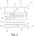
FIG. 3 is an exploded side-elevational view of another embodiment of anelectrochemical cell 10A according to the present invention. -
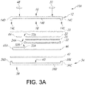
FIG. 3A is an exploded side-elevational view of theelectrochemical cell 10A shown inFIG. 3 , but without thegold metallization ring 50. - As used herein, the term "transparent" is defined as a material having the property of transmitting rays of light through its substance so that bodies situated beyond or behind can be distinctly seen.
- The term "sapphire" is defined as a variety of the mineral corundum, consisting of aluminium oxide (α-Al2O3) with trace amounts of elements such as iron, titanium, chromium, copper, or magnesium. It is typically blue, but can also occur in yellow, purple, orange, and green colors (parti-sapphires show two or more colors). The only color that sapphire cannot be is red - as red colored corundum is called ruby, another corundum variety. Sapphire is a remarkably hard material - 9 on the Mohs scale (the third hardest mineral, after diamond at 10 and moissanite at 9.5), which makes it uniquely suited for use as a casing material according to the present inventions.
- Turning now to the drawings,
FIGs. 1 and 2 illustrate one embodiment of anelectrochemical cell 10 according to the present invention. Theelectrochemical cell 10 comprises a first plate-shapedceramic substrate 12 that is preferably selected from polycrystalline alumina, 3 mol% YSZ, or a single-crystal alumina, and serves as one half of a casing for the cell. Theceramic substrate 12 is a planar structure forming the lid-side of the casing and comprises a lid substrateperipheral edge 14 meeting an outermajor face 16 opposite an innermajor face 18. - Since ceramic substrates are often formed with rough surfaces, which can lead to defective coatings such as interrupted interconnection traces, protrusions which may cause electric shorting between layers, uneven electrochemical reactions leading to poor cycling or dendrite formation, and the like, prior to incorporation into the cell, the
lid ceramic substrate 12 is preferably lapped and polished with slurry or ceramic coated grinding paper followed by diamond polishing. This provides a surface roughness that is greater than zero, but less than 50 nm, and more preferably less than 10 nm. - In the illustrated embodiment, the
peripheral edge 14 of thelid substrate 12 comprises opposed lid first andsecond edge portions fourth edge portions lid substrate 12 has a non-square shape. In any event, the surface area of the outermajor face 16 of thelid substrate 12 ranges from about 1 mm2 to about 10 cm2. - The
lid substrate 12 is provided with ametallization strip 20 that is a continuous or endless strip of titanium, niobium or other metallic material having a ring-shape with an outer edge that is coincident the outer surface of the first, second, third and fourth dependingedge portions lid metallization strip 20 has a width that ranges from about 1 µm to about 250 µm and a thickness that ranges from about 0.1 µm to 25 µm to define a surrounded open area immediately adjacent to the innermajor face 18 of the lid substrate. - A cathode
current collector 22 is deposited as a thin-film layer that contacts the innermajor face 18 of thelid substrate 12, spaced inwardly from thelid metallization strip 20. The cathode current collector is preferably a continuous layer of titanium, devoid of perforations, and has a thickness measured outwardly from the base substrate innermajor face 18 that ranges from about 0.1 µm to about 3 µm. Stainless steel, tantalum, platinum, gold, aluminum, cobalt, molybdenum, nickel, copper, nickel, and alloys thereof are also suitable materials for the cathode current collector. A gap of at least about 1 µm to about 250 µm separates the cathodecurrent collector 22 from thelid metallization strip 20. - A layer of cathode
active material 24 is supported on the cathodecurrent collector 22. The cathodeactive material 24 preferably extends to and is coincident with the outer peripheral edge of thecurrent collector 22. The cathodeactive material 24 has a thickness that ranges from about 1 µm to about 25 µm. Suitable cathode active materials are selected from LiCoO2, LiMnO2, LiMn2O4, LiFePO4, Ag2V4O11, V2O5. -
FIG. 1 further shows that thelid substrate 12 is provided with spaced-apart first andsecond openings lid ceramic substrate 12 is provided with respective perimeter metallizations surrounding theopenings Openings - The
first opening 26 is aligned over the cathodecurrent collector 22 and the cathodeactive material 24 and receives a first gold-braze button 30. In a separate brazing step prior to the cathodeactive material 24 being contacted to the cathodecurrent collector 22, the first gold-braze button 30 forms a hermetic seal with thelid ceramic substrate 12 and has an inner surface that contacts the cathode current collector. An outer surface of the first gold-braze button 30 is substantially co-planar with the lid substrate outermajor face 16 or it extends outwardly about 50 µm above the major face. That way, the first gold-braze button 30 serves as the positive terminal for theelectrochemical cell 10. - A layer of solid electrolyte 32 (LixPOyNz) contacts the cathode
active material layer 24, opposite the cathodecurrent collector 22 and the gold-braze button 30. Thesolid electrolyte layer 32 preferably extends to and curves over or around the outer peripheral edge of the cathodeactive material 24, but it is spaced inwardly from thelid metallization strip 20. Thesolid electrolyte layer 32 has a thickness that ranges from about 1 µm to about 5 µm with the curved peripheral edge contacting the innermajor face 18 of thelid substrate 12. - Separately, a second plate-shaped base
ceramic substrate 34 is selected from polycrystalline alumina, 3 mol% YSZ, and a single-crystal alumina and serves as the other half of the casing for theelectrochemical cell 10. The baseceramic substrate 34 has a peripheral edge 36 meeting an outermajor face 38 opposite an innermajor face 40. - The peripheral edge 36 of the
base substrate 34 comprises a rim that extends upwardly from the innermajor face 40 to thereby provide a recess that is bounded by the opposed first and secondupstanding edge portions 36A and 36B extending to and meeting with the third and fourthupstanding edge portions edge portions upstanding edge surface 36E aligned along an imaginary plane that is parallel to the outer and inner major faces 38, 40 of thebase substrate 34. The edge portions are of substantially equal lengths themselves and are also equal in length to those of the corresponding lid substrate first, second, third andfourth edge portions base substrate 34 with a square shape in plan-view that matches the square shape of thelid substrate 12. In any event, the surface area of the outermajor face 38 of thebase substrate 34 ranges from about 1 mm2 to about 10 cm2. - In alternate embodiments, the
base substrate 34 has a non-square shape that matches that of thelid substrate 12. In that respect, those skilled in the art will readily appreciate that the lid andbase substrates - The
upstanding edge surface 36E of the base ceramic substrate is provided with a surroundingmetallization 42. Thebase substrate metallization 42 is a continuous or endless strip of titanium, niobium or other metallic material having a ring-shape with an outer edge that is coincident the outer surface of the first, second, third andfourth edge portions base substrate 34. The upstanding edge of the base ceramic substrate has a width that ranges from about 1 µm to about 250 µm to define a surrounded open recess immediately adjacent to the innermajor face 40. Thebase metallization strip 42 has a width that ranges from about 1 µm to 250 µm and a thickness 21 that ranges from about 0.1 µm to about 25 µm. -
FIG. 2 illustrates that the cathodecurrent collector 22, cathodeactive material 24 and thesolid electrolyte layer 32 are provided with respective corner cut-outs fourth edge portions lid substrate 12 meet and where the second andfourth edge portions base substrate 34 meet. - The respective corner cut-
outs current collector 22, cathodeactive material 24 and thesolid electrolyte layer 32 provide a space for an anodecurrent collector 44 as a thin-film layer that contacts the innermajor face 18 of thelid substrate 12, spaced from the cathodecurrent collector 22. The anodecurrent collector 44 is a continuous layer, preferably of titanium or copper, that is devoid of perforations, and has a thickness that is comparable to that of the cathodecurrent collector 22. Stainless steel, tantalum, platinum, gold, cobalt, molybdenum, nickel, and alloys thereof are also suitable materials for the anodecurrent collector 44. A gap that ranges from about 1 µm to about 250 µm separates the anodecurrent collector 44 from the cathodecurrent collector 22. - A layer of anode
active material 46 contacts thesolid electrolyte 32 opposite the cathodeactive material 24. The anodeactive material 46 has an extendingportion 46A that laps over thesolid electrolyte 32 to contact the anodecurrent collector 44. Thesolid electrolyte 32 in turn has an upstandingperipheral edge 32B that physically segregates the anodeactive material 46 from the cathodeactive material 24 contacting the cathodecurrent collector 22. The anodeactive material 46 has a thickness that ranges from about 1 µm to about 25 µm, and the combined thickness of the anodecurrent collector 44 and the anodeactive material 46 is somewhat less than the thickness of the anode substrate upstanding peripheral edge 36. Suitable anode active materials include lithium and its alloys and intermetallic compounds including, for example, Li-Si, Li-Sn, Li-Al, Li-B and Li-Si-B alloys, and mixtures and oxides thereof. - In a similar manner as with the gold-
braze terminal button 30 that resides in thefirst opening 26 in thelid substrate 12 and contacts the cathodecurrent collector 22 to thereby serve as the positive terminal for theelectrochemical cell 10, a second gold-braze button 48 resides in thesecond opening 28 in thelid substrate 12. In the brazing step where the first gold-braze button 30 forms a hermetic seal with thelid ceramic substrate 12, the second gold-braze button 48 also forms a hermetic seal with the lid substrate and has an inner surface that contacts the anodecurrent collector 44. An outer surface of the second gold-braze 48 is substantially co-planar with the outermajor face 16 of the lid ceramic substrate or it extends outwardly about 50 µm above the major face. That way, the second gold-braze button 48 serves as the negative terminal for theelectrochemical cell 10. - During final cell assembly, with the
lid substrate 12 supporting the cathodecurrent collector 22, the cathodeactive material 24, thesolid electrolyte 32, the anodecurrent collector 44 and the anodeactive material 46, the lid and base substrates are moved into registry with each other. Anendless gold pre-form 50 having a ring-shape is supported on either thelid metallization strip 20 or thebase metallization strip 42. In either configuration, thecathode substrate 12 and theanode substrate 34 are moved together until thelid metallization strip 20 contacts one side of thegold pre-form 50 and the basesubstrate metallization strip 42 contacts the other side thereof. - The
lid substrate 12 is preferably of a single-crystal alumina (sapphire), which is substantially transparent. The transparentsapphire lid substrate 12 allows that substrate and thebase substrate 34 serving as the two case halves to be joined together by laser welding through the transparent ceramic 12 to melt thegold interlayer pre-form 50 into intimate hermetic contact with the opposed lid and base metallizations strips 20 and 42 to thereby hermetically seal the casing. This facilitates fabrication of electrochemical cells in multi-cell arrays/sheets to make the manufacturing process more cost-effective and practical. -
FIG. 2A illustrates an alternate embodiment of theelectrochemical cell 10 where thegold pre-form 50 has been eliminated. Instead, the lid and base metallization strips 20 and 42 are laser welded together without thegold pre-form 50. In still a further embodiment, gold is sputtered directly onto at least one or both metallization strips 20, 42, and a laser is preferably used to hermetically weld thelid substrate 12 to thebase substrate 34 to thereby hermetically seal the casing. - In an alternate embodiment, the anode and cathode active materials can be switched with each other. In this embodiment,
terminal button 30 conductively contacts the anode current collector andterminal button 48 conductively contacts the cathode current collector. -
FIG. 3 illustrate another embodiment of theelectrochemical cell 10A according to the present invention.Electrochemical cell 10A is similar to theelectrochemical cell 10 shown inFIGs. 1, 2 and2A with the exception that instead of being a planar structure, thelid substrate 12 has a depending rim-shapedperipheral edge 14E. Thebase substrate 34 has the upstanding rim-shapedperipheral edge 36E previously described with respect toFIGs. 2 and2A . This means that the combined height ofedges cell 10A inFIG. 3 is substantially equal to the height of the dependingedge 14E inFIGs. 2 and2A . In all other aspects, thecells - In a similar manner as with the
cell 10 illustrated inFIG. 2A where the lid and base metallization strips 20 and 42 are laser welded together without thegold pre-form 50,FIG. 3A illustrates a similar embodiment, but with thelid substrate 12 having a depending rim-shapedperipheral edge 14E. As before, gold is sputtered directly onto at least one or both the lid and base metallization strips 20, 42, and a laser is preferably used to hermetically weld thelid substrate 12 to thebase substrate 34 to thereby hermetically seal the casing. - Thus, with the outer major faces 16 and 38 of the respective lid and
base substrates major face 16 of thelid substrate 12 to the outermajor face 38 of thebase substrate 34 ranging from about 250 µm to about 2.5 mm, thecells - It is appreciated that various modifications to the inventive concepts described herein may be apparent to those of ordinary skill in the art without departing from the spirit and scope of the present invention as defined by the appended claims.
Claims (25)
- An electrochemical cell, comprising:a) a ceramic casing, comprising:i) a first ceramic substrate having a first peripheral edge extending to and meeting with opposed first substrate outer and inner major faces;ii) a first ring-shaped metallization contacting the first substrate inner major face adjacent to the first substrate peripheral edge;iii) a second ceramic substrate having a second substrate peripheral edge extending to and meeting with opposed second substrate outer and inner major faces; andiv) a second ring-shaped metallization contacting the second substrate inner major face adjacent to the second substrate peripheral edge;b) a first electrode current collector contacting the first substrate inner major face, spaced inwardly from the first ring-shaped metallization;c) a first electrode active material contacting the first electrode current collector;d) a second electrode current collector contacting the first substrate inner major face, spaced inwardly from the first ring-shaped metallization, wherein the second electrode current collector is side-by-side with the first electrode current collector;e) a solid electrolyte contacting the first electrode active material;f) a second electrode active material contacting the second electrode current collector and contacting the solid electrolyte opposite the first electrode active material;g) a first opening extending through the first ceramic substrate in alignment with the first electrode current collector, wherein a first gold body hermetically sealed to the first ceramic substrate in the first opening conductively contacts the first electrode current collector to thereby serve as a first terminal; andh) a second opening extending through the first ceramic substrate in alignment with the second electrode current collector, wherein a second gold body hermetically sealed to the first ceramic substrate in the second opening conductively contacts the second electrode current collector to thereby serve as a second, opposite polarity terminal for the electrochemical cell,i) wherein the first and second ring-shaped metallizations are in a hermetically sealed relationship with each other to thereby hermetically seal the first and second ceramic substrates together to form the casing.
- The electrochemical cell of claim 1, wherein the first electrode is a cathode and the second electrode is an anode, or the first electrode is an anode and the second electrode is a cathode.
- The electrochemical cell of one of claims 1 or 2, wherein the outer and inner major faces of the first ceramic substrate are both substantially planar.
- The electrochemical cell of one of claims 1 to 3, wherein the first and second ring-shaped metallizations are of titanium or niobium.
- The electrochemical cell of one of claims 1 to 4, wherein the first and second openings extending through the first ceramic substrate are each provided with a metallization of titanium or niobium, and wherein the respective first and second gold bodies are hermetically sealed to the respective first and second metallizations in the first and second openings.
- The electrochemical cell of one of claims 1 to 5, wherein both the first and second ceramic substrates have an extending peripheral rim supporting the respective first and second ring-shaped metallization.
- The electrochemical cell of one of claims 1 to 6, wherein the solid electrolyte contacting the first electrode active material opposite the first electrode current collector does not contact the second electrode current collector.
- The electrochemical cell of one of claims 1 to 7, wherein a gold layer hermetically seals the first and second ring-shaped metallizations together to thereby hermetically seal the first and second ceramic substrates to each other.
- The electrochemical cell of one of claims 1 to 8, wherein the first and second ring-shaped metallizations are hermetically sealed to each other to thereby hermetically seal the first and second ceramic substrates together to form the casing.
- The electrochemical cell of one of claims 1 to 9, wherein at least one of the first and second ceramic substrates has an extending peripheral rim supporting the respective first and second ring-shaped metallization, and wherein, with the first and second ring-shaped metallizations being hermetically sealed to each other to thereby hermetically seal the first and second ceramic substrates together, a sum of a first thickness of the first electrode current collector, a second thickness of the first electrode active material, a third thickness of the solid electrolyte, a fourth thickness of the second electrode active material and a fifth thickness of the second electrode current collector is less than the distance from the first ceramic substrate inner major face to the second ceramic substrate inner major face.
- The electrochemical cell of one of claims 1 to 10, wherein at least one of the first and second ceramic substrates has an extending peripheral rim supporting the respective first and second ring-shaped metallization, and wherein, with a gold layer hermetically sealing the first and second ring-shaped metallizations together to thereby hermetically seal the first and second ceramic substrates to each other, a sum of a first thickness of the first electrode current collector, a second thickness of the first electrode active material, a third thickness of the solid electrolyte, a fourth thickness of the second electrode active material and a fifth thickness of the second electrode current collector is less than the distance from the first ceramic substrate inner major face to the second ceramic substrate inner major face.
- The electrochemical cell of one of claims 10 or 11, wherein the sum of the first, second, third, fourth and fifth thicknesses is less than the distance from the first ceramic substrate inner major face to the second ceramic substrate inner major face by about 1 µm to 100 µm.
- The electrochemical cell of one of claims 1 to 12, wherein the first and second current collectors are individually selected from the group consisting of titanium, copper, stainless steel, tantalum, platinum, gold, aluminum, cobalt, molybdenum, nickel, and alloys thereof.
- The electrochemical cell of one of claims 1 to 13, wherein at least the first and second inner major faces of the respective first and second ceramic substrates have a surface roughness that is greater than zero, but less than 50 nm.
- The electrochemical cell of one of claims 1 to 14, wherein the solid electrolyte extends between the first and second electrode current collectors.
- The electrochemical cell of one of claims 1 to 15, wherein the first and second ceramic substrates are selected from the group consisting of 3 mol% YSZ, polycrystalline alumina, and sapphire.
- The electrochemical cell of one of claims 1 to 16, wherein at least one of the first and second ceramic substrates is of a substantially transparent sapphire.
- The electrochemical cell of one of claims 1 to 17, wherein the anode active material is selected from the group consisting of lithium, Li-Si, Li-Sn, Li-Al, Li-B and Li-Si-B alloys, and wherein the cathode active material is selected from the group consisting of LiCoO2, LiMnO2, LiMn2O4, LiFePO4, Ag2V4O11, V2O5, and mixtures thereof.
- The electrochemical cell of one of claims 1 to 18, wherein the solid electrolyte comprises LixPOyNz.
- The electrochemical cell of one of claims 1 to 19 having a total volume that is less than 0.5 cc.
- An electrochemical cell, comprising:a) a ceramic casing, comprising:i) a first sapphire substrate having a first peripheral edge extending to and meeting with opposed first substrate outer and inner major faces;ii) a first ring-shaped metallization contacting the first sapphire substrate inner major face adjacent to the first substrate peripheral edge;iii) a second ceramic substrate having a second substrate peripheral rim extending to and meeting with opposed second substrate outer and inner major faces; andiv) a second ring-shaped metallization contacting the second substrate peripheral rim;b) a first electrode current collector contacting the first sapphire substrate inner major face, spaced inwardly from the first ring-shaped metallization;c) a first electrode active material contacting the first electrode current collector;d) a second electrode current collector contacting the first sapphire substrate inner major face, spaced inwardly from the first ring-shaped metallization, wherein the second electrode current collector is side-by-side with the first electrode current collector;e) a solid electrolyte contacting the first electrode active material;f) a second electrode active material contacting the second electrode current collector and contacting the solid electrolyte opposite the first electrode active material;g) a first opening extending through the first sapphire substrate in alignment with the first electrode current collector, wherein a first gold body hermetically sealed to the first sapphire substrate in the first opening conductively contacts the first electrode current collector to thereby serve as a first terminal; andh) a second opening extending through the first sapphire substrate in alignment with the second electrode current collector, wherein a second gold body hermetically sealed to the first sapphire substrate in the second opening conductively contacts the second electrode current collector to thereby serve as a second, opposite polarity terminal for the electrochemical cell.
- The electrochemical cell of claim 21, wherein the first electrode is a cathode and the second electrode is an anode, or the first electrode is an anode and the second electrode is a cathode.
- The electrochemical cell of one of claims 21 or 22, wherein at least one of the first and second ceramic substrates is of a substantially transparent sapphire.
- An electrochemical cell, comprising:a) an electrode assembly comprising:i) an anode comprising an anode active material conductively contacted to an anode current collector; andii) a cathode comprising a cathode active material conductively contacted to a cathode current collector,iii) wherein the anode and cathode are segregated from direct physical contact with each other and activated with an electrolyte; andb) a ceramic casing housing the electrode assembly, the casing comprising:i) a first ceramic substrate having a first peripheral edge extending to and meeting with opposed first substrate outer and inner major faces;ii) a first ring-shaped metallization contacting the first substrate inner major face adjacent to the first substrate peripheral edge;iii) a second ceramic substrate having a second substrate peripheral edge extending to and meeting with opposed second substrate outer and inner major faces; andiv) a second ring-shaped metallization contacting the second substrate inner major face adjacent to the second substrate peripheral edge,v) wherein the first and second ring-shaped metallizations are in a hermetically sealed relationship with each other to thereby hermetically seal the first and second ceramic substrates together to form the casing;c) a first opening extending through the first ceramic substrate in alignment with the anode current collector, wherein a first gold body hermetically sealed to the first ceramic substrate in the first opening conductively contacts the anode current collector to thereby serve as a negative terminal; andd) a second opening extending through the first ceramic substrate in alignment with the cathode current collector, wherein a second gold body hermetically sealed to the first ceramic substrate in the second opening conductively contacts the cathode current collector to thereby serve as a positive terminal for the electrochemical cell.
- The electrochemical cell of claim 24, wherein at least one of the first and second ceramic substrates is of a substantially transparent sapphire.
Applications Claiming Priority (1)
| Application Number | Priority Date | Filing Date | Title |
|---|---|---|---|
| US201862614623P | 2018-01-08 | 2018-01-08 |
Publications (2)
| Publication Number | Publication Date |
|---|---|
| EP3509125A1 true EP3509125A1 (en) | 2019-07-10 |
| EP3509125B1 EP3509125B1 (en) | 2021-02-24 |
Family
ID=65010592
Family Applications (1)
| Application Number | Title | Priority Date | Filing Date |
|---|---|---|---|
| EP19150718.5A Not-in-force EP3509125B1 (en) | 2018-01-08 | 2019-01-08 | Hermetic thin film electrochemical cells housed in a ceramic casing and activated with a solid electrolyte |
Country Status (2)
| Country | Link |
|---|---|
| US (2) | US11011787B2 (en) |
| EP (1) | EP3509125B1 (en) |
Families Citing this family (2)
| Publication number | Priority date | Publication date | Assignee | Title |
|---|---|---|---|---|
| US20230361395A1 (en) * | 2022-05-06 | 2023-11-09 | Greatbatch Ltd. | Miniature Electrical Power Source Housed In A Casing Having An Intermediate Ceramic Ring Diffusion Bonded To Opposed Titanium Members |
| KR20260038352A (en) * | 2024-09-11 | 2026-03-19 | 삼성에스디아이 주식회사 | Cap assembly, secondary battery and method for manufacturing secondary battery |
Citations (6)
| Publication number | Priority date | Publication date | Assignee | Title |
|---|---|---|---|---|
| EP0269007A1 (en) * | 1986-11-28 | 1988-06-01 | Siemens Aktiengesellschaft | Ceramic-metal feedthrough assembly, in particular for cardiac or neural stimulation, and method of manufacturing it |
| US20050007718A1 (en) * | 2003-02-27 | 2005-01-13 | Stevenson Robert A. | EMI filter terminal assembly with wire bond pads for human implant applications |
| DE102011103975A1 (en) * | 2011-06-10 | 2012-12-13 | Schott Ag | Feed-through component for feeding conductors for lithium ion battery used for portable electronic device, has electrode connecting portion which are mechanically connected with head portions through welding process |
| US8642887B1 (en) * | 2010-12-03 | 2014-02-04 | Greatbatch Ltd. | Metallization barrier for a hermetic feedthrough |
| US8815450B1 (en) * | 2008-01-28 | 2014-08-26 | Oak Ridge Micro-Energy, Inc. | Low voltage thin film batteries |
| US20150004478A1 (en) * | 2010-04-29 | 2015-01-01 | Greatbatch Ltd. | Novel Method For Gold Plated Termination of Hermetic Device |
Family Cites Families (25)
| Publication number | Priority date | Publication date | Assignee | Title |
|---|---|---|---|---|
| US5338625A (en) | 1992-07-29 | 1994-08-16 | Martin Marietta Energy Systems, Inc. | Thin film battery and method for making same |
| US6268079B1 (en) | 1998-11-25 | 2001-07-31 | Japan Storage Battery Co., Ltd. | Nonaqueous-electrolyte battery |
| US6782290B2 (en) | 2001-04-27 | 2004-08-24 | Medtronic, Inc. | Implantable medical device with rechargeable thin-film microbattery power source |
| US6818356B1 (en) | 2002-07-09 | 2004-11-16 | Oak Ridge Micro-Energy, Inc. | Thin film battery and electrolyte therefor |
| EP1441400B1 (en) | 2003-01-17 | 2009-11-04 | Greatbatch Ltd. | Hermetically sealed coin cell |
| FR2874128B1 (en) | 2004-08-03 | 2006-10-13 | Commissariat Energie Atomique | MICROBATTERY COMPRISING THROUGH CONNECTIONS AND METHOD OF MAKING SUCH A MICROBATTERY |
| US8679674B2 (en) | 2005-03-25 | 2014-03-25 | Front Edge Technology, Inc. | Battery with protective packaging |
| US7524577B2 (en) | 2005-09-06 | 2009-04-28 | Oak Ridge Micro-Energy, Inc. | Long life thin film battery and method therefor |
| US7553582B2 (en) | 2005-09-06 | 2009-06-30 | Oak Ridge Micro-Energy, Inc. | Getters for thin film battery hermetic package |
| FR2925227B1 (en) | 2007-12-12 | 2009-11-27 | Commissariat Energie Atomique | ENCASPULATED LITHIUM ELECTROCHEMICAL DEVICE. |
| FR2938977B1 (en) | 2008-11-21 | 2011-04-01 | Commissariat Energie Atomique | MICROBATTERY ON MONOLITHIC ENCAPSULATION SUBSTRATE |
| FR2946461B1 (en) | 2009-06-09 | 2011-07-22 | Commissariat Energie Atomique | DEVICE FOR FLEXIBLE ENCAPSULATION OF A MICRO-BATTERY |
| EP2426750B1 (en) | 2010-09-07 | 2012-11-14 | swissbatt AG | Battery cell casing |
| EP2469620B1 (en) | 2010-12-24 | 2013-08-14 | swissbatt AG | Battery |
| US8865340B2 (en) | 2011-10-20 | 2014-10-21 | Front Edge Technology Inc. | Thin film battery packaging formed by localized heating |
| EP3366348B1 (en) | 2012-01-16 | 2023-08-23 | Greatbatch Ltd. | Emi filtered co-connected hermetic feedthrough, feedthrough capacitor and leadwire assembly for an active implantable medical device |
| US9887403B2 (en) | 2013-03-15 | 2018-02-06 | Apple Inc. | Thin film encapsulation battery systems |
| US9318774B2 (en) | 2013-06-28 | 2016-04-19 | Google Inc. | Substrate for solid-state battery |
| US9455423B2 (en) | 2014-01-24 | 2016-09-27 | Verily Life Sciences Llc | Battery |
| US9793522B2 (en) | 2014-08-13 | 2017-10-17 | Verily Life Sciences Llc | Sealed solid state battery |
| US9599842B2 (en) | 2014-08-21 | 2017-03-21 | Johnson & Johnson Vision Care, Inc. | Device and methods for sealing and encapsulation for biocompatible energization elements |
| US9991550B2 (en) | 2015-02-27 | 2018-06-05 | Verily Life Sciences Llc | Methods and devices associated with bonding of solid-state lithium batteries |
| US10052492B2 (en) | 2015-05-06 | 2018-08-21 | Verily Life Sciences Llc | Replaceable battery for implantable devices |
| US10044009B2 (en) | 2016-09-08 | 2018-08-07 | Stmicroelectronics (Tours) Sas | Encapsulated microbattery having terminal connected to active layer through a via |
| US20180108496A1 (en) * | 2016-10-19 | 2018-04-19 | Sagar Venkateswaran | Method of Assembly of Electrochemical Cells for High Temperature Applications |
-
2019
- 2019-01-04 US US16/240,173 patent/US11011787B2/en active Active
- 2019-01-08 EP EP19150718.5A patent/EP3509125B1/en not_active Not-in-force
-
2020
- 2020-02-12 US US16/788,679 patent/US11527795B2/en active Active
Patent Citations (6)
| Publication number | Priority date | Publication date | Assignee | Title |
|---|---|---|---|---|
| EP0269007A1 (en) * | 1986-11-28 | 1988-06-01 | Siemens Aktiengesellschaft | Ceramic-metal feedthrough assembly, in particular for cardiac or neural stimulation, and method of manufacturing it |
| US20050007718A1 (en) * | 2003-02-27 | 2005-01-13 | Stevenson Robert A. | EMI filter terminal assembly with wire bond pads for human implant applications |
| US8815450B1 (en) * | 2008-01-28 | 2014-08-26 | Oak Ridge Micro-Energy, Inc. | Low voltage thin film batteries |
| US20150004478A1 (en) * | 2010-04-29 | 2015-01-01 | Greatbatch Ltd. | Novel Method For Gold Plated Termination of Hermetic Device |
| US8642887B1 (en) * | 2010-12-03 | 2014-02-04 | Greatbatch Ltd. | Metallization barrier for a hermetic feedthrough |
| DE102011103975A1 (en) * | 2011-06-10 | 2012-12-13 | Schott Ag | Feed-through component for feeding conductors for lithium ion battery used for portable electronic device, has electrode connecting portion which are mechanically connected with head portions through welding process |
Also Published As
| Publication number | Publication date |
|---|---|
| EP3509125B1 (en) | 2021-02-24 |
| US11527795B2 (en) | 2022-12-13 |
| US11011787B2 (en) | 2021-05-18 |
| US20190214605A1 (en) | 2019-07-11 |
| US20200185662A1 (en) | 2020-06-11 |
Similar Documents
| Publication | Publication Date | Title |
|---|---|---|
| EP2850675B1 (en) | Electrochemical cells | |
| CN100517802C (en) | Thin Alkaline Batteries | |
| EP2840638B1 (en) | Electrode assembly, and battery cell and device comprising same | |
| KR101357092B1 (en) | Thin film battery with protective packaging | |
| US8790801B2 (en) | Integrated electrochemical and solar cell | |
| EP1914820B1 (en) | Battery module | |
| KR101379958B1 (en) | Lectrode assembly, battery cell, manufacturing mathod of electrode assembly and manufacturing mathod of battery cell | |
| KR100982468B1 (en) | High capacity thin film battery module and its manufacturing method | |
| EP1318561A1 (en) | Coin-shaped battery | |
| JP2006512745A5 (en) | ||
| JP2002042863A (en) | Thin-film solid-state lithium-ion secondary battery | |
| US4287273A (en) | Plural cell battery structure | |
| US20200052342A1 (en) | Lithium-ion rechargeable battery | |
| CN113675508A (en) | Batteries and Electronic Equipment | |
| US11527795B2 (en) | Hermetic weld for a thin film electrochemical cell activated with a solid electrolyte and housed in a ceramic casing | |
| KR101161154B1 (en) | Thin film battery contaning substrate with extention metal and multi-layered thin film battery module fabricated using the same | |
| JP2017152247A (en) | All-solid type electrode body and electrochemical cell | |
| US20220376290A1 (en) | Method For Providing A Substrate With Hermetic Vias For A Thin Film Electrochemical Cell Activated With A Solid Electrolyte And Housed In A Ceramic Casing | |
| JP2011258477A (en) | Nonaqueous electrolyte battery | |
| US11114714B2 (en) | Miniature electrochemical cell having a casing of a metal container closed with a ceramic plate having two via holes supporting opposite polarity platinum-containing conductive pathways | |
| CN215933699U (en) | Battery and electronic equipment | |
| US11251480B2 (en) | Miniature electrochemical cell having a casing of a conductive plate closing an open-ended ceramic container having two via holes supporting opposite polarity platinum-containing conductive pathways | |
| EP4274007A2 (en) | Miniature electrical power source housed in a casing having an intermediate ceramic ring diffusion bonded to opposed titanium members | |
| KR102941552B1 (en) | Method of producing all-solid-state battery and all-solid-state battery | |
| US20240387878A1 (en) | Lithium secondary battery |
Legal Events
| Date | Code | Title | Description |
|---|---|---|---|
| PUAI | Public reference made under article 153(3) epc to a published international application that has entered the european phase |
Free format text: ORIGINAL CODE: 0009012 |
|
| STAA | Information on the status of an ep patent application or granted ep patent |
Free format text: STATUS: THE APPLICATION HAS BEEN PUBLISHED |
|
| AK | Designated contracting states |
Kind code of ref document: A1 Designated state(s): AL AT BE BG CH CY CZ DE DK EE ES FI FR GB GR HR HU IE IS IT LI LT LU LV MC MK MT NL NO PL PT RO RS SE SI SK SM TR |
|
| AX | Request for extension of the european patent |
Extension state: BA ME |
|
| STAA | Information on the status of an ep patent application or granted ep patent |
Free format text: STATUS: REQUEST FOR EXAMINATION WAS MADE |
|
| 17P | Request for examination filed |
Effective date: 20191125 |
|
| RBV | Designated contracting states (corrected) |
Designated state(s): AL AT BE BG CH CY CZ DE DK EE ES FI FR GB GR HR HU IE IS IT LI LT LU LV MC MK MT NL NO PL PT RO RS SE SI SK SM TR |
|
| STAA | Information on the status of an ep patent application or granted ep patent |
Free format text: STATUS: EXAMINATION IS IN PROGRESS |
|
| 17Q | First examination report despatched |
Effective date: 20200306 |
|
| GRAP | Despatch of communication of intention to grant a patent |
Free format text: ORIGINAL CODE: EPIDOSNIGR1 |
|
| STAA | Information on the status of an ep patent application or granted ep patent |
Free format text: STATUS: GRANT OF PATENT IS INTENDED |
|
| INTG | Intention to grant announced |
Effective date: 20200814 |
|
| GRAS | Grant fee paid |
Free format text: ORIGINAL CODE: EPIDOSNIGR3 |
|
| GRAA | (expected) grant |
Free format text: ORIGINAL CODE: 0009210 |
|
| STAA | Information on the status of an ep patent application or granted ep patent |
Free format text: STATUS: THE PATENT HAS BEEN GRANTED |
|
| AK | Designated contracting states |
Kind code of ref document: B1 Designated state(s): AL AT BE BG CH CY CZ DE DK EE ES FI FR GB GR HR HU IE IS IT LI LT LU LV MC MK MT NL NO PL PT RO RS SE SI SK SM TR |
|
| REG | Reference to a national code |
Ref country code: CH Ref legal event code: EP |
|
| REG | Reference to a national code |
Ref country code: AT Ref legal event code: REF Ref document number: 1365600 Country of ref document: AT Kind code of ref document: T Effective date: 20210315 |
|
| REG | Reference to a national code |
Ref country code: IE Ref legal event code: FG4D |
|
| REG | Reference to a national code |
Ref country code: DE Ref legal event code: R096 Ref document number: 602019002637 Country of ref document: DE |
|
| REG | Reference to a national code |
Ref country code: LT Ref legal event code: MG9D |
|
| REG | Reference to a national code |
Ref country code: NL Ref legal event code: MP Effective date: 20210224 |
|
| PG25 | Lapsed in a contracting state [announced via postgrant information from national office to epo] |
Ref country code: LT Free format text: LAPSE BECAUSE OF FAILURE TO SUBMIT A TRANSLATION OF THE DESCRIPTION OR TO PAY THE FEE WITHIN THE PRESCRIBED TIME-LIMIT Effective date: 20210224 Ref country code: NO Free format text: LAPSE BECAUSE OF FAILURE TO SUBMIT A TRANSLATION OF THE DESCRIPTION OR TO PAY THE FEE WITHIN THE PRESCRIBED TIME-LIMIT Effective date: 20210524 Ref country code: PT Free format text: LAPSE BECAUSE OF FAILURE TO SUBMIT A TRANSLATION OF THE DESCRIPTION OR TO PAY THE FEE WITHIN THE PRESCRIBED TIME-LIMIT Effective date: 20210624 Ref country code: BG Free format text: LAPSE BECAUSE OF FAILURE TO SUBMIT A TRANSLATION OF THE DESCRIPTION OR TO PAY THE FEE WITHIN THE PRESCRIBED TIME-LIMIT Effective date: 20210524 Ref country code: GR Free format text: LAPSE BECAUSE OF FAILURE TO SUBMIT A TRANSLATION OF THE DESCRIPTION OR TO PAY THE FEE WITHIN THE PRESCRIBED TIME-LIMIT Effective date: 20210525 Ref country code: HR Free format text: LAPSE BECAUSE OF FAILURE TO SUBMIT A TRANSLATION OF THE DESCRIPTION OR TO PAY THE FEE WITHIN THE PRESCRIBED TIME-LIMIT Effective date: 20210224 Ref country code: FI Free format text: LAPSE BECAUSE OF FAILURE TO SUBMIT A TRANSLATION OF THE DESCRIPTION OR TO PAY THE FEE WITHIN THE PRESCRIBED TIME-LIMIT Effective date: 20210224 |
|
| REG | Reference to a national code |
Ref country code: AT Ref legal event code: MK05 Ref document number: 1365600 Country of ref document: AT Kind code of ref document: T Effective date: 20210224 |
|
| PG25 | Lapsed in a contracting state [announced via postgrant information from national office to epo] |
Ref country code: SE Free format text: LAPSE BECAUSE OF FAILURE TO SUBMIT A TRANSLATION OF THE DESCRIPTION OR TO PAY THE FEE WITHIN THE PRESCRIBED TIME-LIMIT Effective date: 20210224 Ref country code: NL Free format text: LAPSE BECAUSE OF FAILURE TO SUBMIT A TRANSLATION OF THE DESCRIPTION OR TO PAY THE FEE WITHIN THE PRESCRIBED TIME-LIMIT Effective date: 20210224 Ref country code: RS Free format text: LAPSE BECAUSE OF FAILURE TO SUBMIT A TRANSLATION OF THE DESCRIPTION OR TO PAY THE FEE WITHIN THE PRESCRIBED TIME-LIMIT Effective date: 20210224 Ref country code: PL Free format text: LAPSE BECAUSE OF FAILURE TO SUBMIT A TRANSLATION OF THE DESCRIPTION OR TO PAY THE FEE WITHIN THE PRESCRIBED TIME-LIMIT Effective date: 20210224 Ref country code: LV Free format text: LAPSE BECAUSE OF FAILURE TO SUBMIT A TRANSLATION OF THE DESCRIPTION OR TO PAY THE FEE WITHIN THE PRESCRIBED TIME-LIMIT Effective date: 20210224 |
|
| PG25 | Lapsed in a contracting state [announced via postgrant information from national office to epo] |
Ref country code: IS Free format text: LAPSE BECAUSE OF FAILURE TO SUBMIT A TRANSLATION OF THE DESCRIPTION OR TO PAY THE FEE WITHIN THE PRESCRIBED TIME-LIMIT Effective date: 20210624 |
|
| PG25 | Lapsed in a contracting state [announced via postgrant information from national office to epo] |
Ref country code: AT Free format text: LAPSE BECAUSE OF FAILURE TO SUBMIT A TRANSLATION OF THE DESCRIPTION OR TO PAY THE FEE WITHIN THE PRESCRIBED TIME-LIMIT Effective date: 20210224 Ref country code: SM Free format text: LAPSE BECAUSE OF FAILURE TO SUBMIT A TRANSLATION OF THE DESCRIPTION OR TO PAY THE FEE WITHIN THE PRESCRIBED TIME-LIMIT Effective date: 20210224 Ref country code: CZ Free format text: LAPSE BECAUSE OF FAILURE TO SUBMIT A TRANSLATION OF THE DESCRIPTION OR TO PAY THE FEE WITHIN THE PRESCRIBED TIME-LIMIT Effective date: 20210224 Ref country code: EE Free format text: LAPSE BECAUSE OF FAILURE TO SUBMIT A TRANSLATION OF THE DESCRIPTION OR TO PAY THE FEE WITHIN THE PRESCRIBED TIME-LIMIT Effective date: 20210224 |
|
| REG | Reference to a national code |
Ref country code: DE Ref legal event code: R097 Ref document number: 602019002637 Country of ref document: DE |
|
| PG25 | Lapsed in a contracting state [announced via postgrant information from national office to epo] |
Ref country code: DK Free format text: LAPSE BECAUSE OF FAILURE TO SUBMIT A TRANSLATION OF THE DESCRIPTION OR TO PAY THE FEE WITHIN THE PRESCRIBED TIME-LIMIT Effective date: 20210224 Ref country code: SK Free format text: LAPSE BECAUSE OF FAILURE TO SUBMIT A TRANSLATION OF THE DESCRIPTION OR TO PAY THE FEE WITHIN THE PRESCRIBED TIME-LIMIT Effective date: 20210224 Ref country code: RO Free format text: LAPSE BECAUSE OF FAILURE TO SUBMIT A TRANSLATION OF THE DESCRIPTION OR TO PAY THE FEE WITHIN THE PRESCRIBED TIME-LIMIT Effective date: 20210224 |
|
| PLBE | No opposition filed within time limit |
Free format text: ORIGINAL CODE: 0009261 |
|
| STAA | Information on the status of an ep patent application or granted ep patent |
Free format text: STATUS: NO OPPOSITION FILED WITHIN TIME LIMIT |
|
| PG25 | Lapsed in a contracting state [announced via postgrant information from national office to epo] |
Ref country code: ES Free format text: LAPSE BECAUSE OF FAILURE TO SUBMIT A TRANSLATION OF THE DESCRIPTION OR TO PAY THE FEE WITHIN THE PRESCRIBED TIME-LIMIT Effective date: 20210224 Ref country code: AL Free format text: LAPSE BECAUSE OF FAILURE TO SUBMIT A TRANSLATION OF THE DESCRIPTION OR TO PAY THE FEE WITHIN THE PRESCRIBED TIME-LIMIT Effective date: 20210224 |
|
| 26N | No opposition filed |
Effective date: 20211125 |
|
| PG25 | Lapsed in a contracting state [announced via postgrant information from national office to epo] |
Ref country code: SI Free format text: LAPSE BECAUSE OF FAILURE TO SUBMIT A TRANSLATION OF THE DESCRIPTION OR TO PAY THE FEE WITHIN THE PRESCRIBED TIME-LIMIT Effective date: 20210224 |
|
| PG25 | Lapsed in a contracting state [announced via postgrant information from national office to epo] |
Ref country code: IT Free format text: LAPSE BECAUSE OF FAILURE TO SUBMIT A TRANSLATION OF THE DESCRIPTION OR TO PAY THE FEE WITHIN THE PRESCRIBED TIME-LIMIT Effective date: 20210224 |
|
| PG25 | Lapsed in a contracting state [announced via postgrant information from national office to epo] |
Ref country code: IS Free format text: LAPSE BECAUSE OF FAILURE TO SUBMIT A TRANSLATION OF THE DESCRIPTION OR TO PAY THE FEE WITHIN THE PRESCRIBED TIME-LIMIT Effective date: 20210624 |
|
| PG25 | Lapsed in a contracting state [announced via postgrant information from national office to epo] |
Ref country code: MC Free format text: LAPSE BECAUSE OF FAILURE TO SUBMIT A TRANSLATION OF THE DESCRIPTION OR TO PAY THE FEE WITHIN THE PRESCRIBED TIME-LIMIT Effective date: 20210224 |
|
| REG | Reference to a national code |
Ref country code: CH Ref legal event code: PL |
|
| REG | Reference to a national code |
Ref country code: BE Ref legal event code: MM Effective date: 20220131 |
|
| PG25 | Lapsed in a contracting state [announced via postgrant information from national office to epo] |
Ref country code: LU Free format text: LAPSE BECAUSE OF NON-PAYMENT OF DUE FEES Effective date: 20220108 |
|
| PG25 | Lapsed in a contracting state [announced via postgrant information from national office to epo] |
Ref country code: BE Free format text: LAPSE BECAUSE OF NON-PAYMENT OF DUE FEES Effective date: 20220131 |
|
| PG25 | Lapsed in a contracting state [announced via postgrant information from national office to epo] |
Ref country code: LI Free format text: LAPSE BECAUSE OF NON-PAYMENT OF DUE FEES Effective date: 20220131 Ref country code: CH Free format text: LAPSE BECAUSE OF NON-PAYMENT OF DUE FEES Effective date: 20220131 |
|
| PG25 | Lapsed in a contracting state [announced via postgrant information from national office to epo] |
Ref country code: IE Free format text: LAPSE BECAUSE OF NON-PAYMENT OF DUE FEES Effective date: 20220108 |
|
| PGFP | Annual fee paid to national office [announced via postgrant information from national office to epo] |
Ref country code: FR Payment date: 20221208 Year of fee payment: 5 |
|
| PGFP | Annual fee paid to national office [announced via postgrant information from national office to epo] |
Ref country code: DE Payment date: 20221130 Year of fee payment: 5 |
|
| GBPC | Gb: european patent ceased through non-payment of renewal fee |
Effective date: 20230108 |
|
| PG25 | Lapsed in a contracting state [announced via postgrant information from national office to epo] |
Ref country code: GB Free format text: LAPSE BECAUSE OF NON-PAYMENT OF DUE FEES Effective date: 20230108 |
|
| PG25 | Lapsed in a contracting state [announced via postgrant information from national office to epo] |
Ref country code: HU Free format text: LAPSE BECAUSE OF FAILURE TO SUBMIT A TRANSLATION OF THE DESCRIPTION OR TO PAY THE FEE WITHIN THE PRESCRIBED TIME-LIMIT; INVALID AB INITIO Effective date: 20190108 |
|
| PG25 | Lapsed in a contracting state [announced via postgrant information from national office to epo] |
Ref country code: MK Free format text: LAPSE BECAUSE OF FAILURE TO SUBMIT A TRANSLATION OF THE DESCRIPTION OR TO PAY THE FEE WITHIN THE PRESCRIBED TIME-LIMIT Effective date: 20210224 Ref country code: CY Free format text: LAPSE BECAUSE OF FAILURE TO SUBMIT A TRANSLATION OF THE DESCRIPTION OR TO PAY THE FEE WITHIN THE PRESCRIBED TIME-LIMIT Effective date: 20210224 |
|
| PG25 | Lapsed in a contracting state [announced via postgrant information from national office to epo] |
Ref country code: TR Free format text: LAPSE BECAUSE OF FAILURE TO SUBMIT A TRANSLATION OF THE DESCRIPTION OR TO PAY THE FEE WITHIN THE PRESCRIBED TIME-LIMIT Effective date: 20210224 |
|
| REG | Reference to a national code |
Ref country code: DE Ref legal event code: R119 Ref document number: 602019002637 Country of ref document: DE |
|
| PG25 | Lapsed in a contracting state [announced via postgrant information from national office to epo] |
Ref country code: MT Free format text: LAPSE BECAUSE OF FAILURE TO SUBMIT A TRANSLATION OF THE DESCRIPTION OR TO PAY THE FEE WITHIN THE PRESCRIBED TIME-LIMIT Effective date: 20210224 |
|
| PG25 | Lapsed in a contracting state [announced via postgrant information from national office to epo] |
Ref country code: DE Free format text: LAPSE BECAUSE OF NON-PAYMENT OF DUE FEES Effective date: 20240801 |
|
| PG25 | Lapsed in a contracting state [announced via postgrant information from national office to epo] |
Ref country code: FR Free format text: LAPSE BECAUSE OF NON-PAYMENT OF DUE FEES Effective date: 20240131 |
|
| PG25 | Lapsed in a contracting state [announced via postgrant information from national office to epo] |
Ref country code: FR Free format text: LAPSE BECAUSE OF NON-PAYMENT OF DUE FEES Effective date: 20240131 Ref country code: DE Free format text: LAPSE BECAUSE OF NON-PAYMENT OF DUE FEES Effective date: 20240801 |