EP3509067A1 - Management method of real-time access to a differential memory, differential memory, and electronic system including the differential memory - Google Patents
Management method of real-time access to a differential memory, differential memory, and electronic system including the differential memory Download PDFInfo
- Publication number
- EP3509067A1 EP3509067A1 EP19150401.8A EP19150401A EP3509067A1 EP 3509067 A1 EP3509067 A1 EP 3509067A1 EP 19150401 A EP19150401 A EP 19150401A EP 3509067 A1 EP3509067 A1 EP 3509067A1
- Authority
- EP
- European Patent Office
- Prior art keywords
- logic data
- memory module
- memory
- main memory
- fetching
- Prior art date
- Legal status (The legal status is an assumption and is not a legal conclusion. Google has not performed a legal analysis and makes no representation as to the accuracy of the status listed.)
- Granted
Links
Images




Classifications
-
- G—PHYSICS
- G11—INFORMATION STORAGE
- G11C—STATIC STORES
- G11C13/00—Digital stores characterised by the use of storage elements not covered by groups G11C11/00, G11C23/00, or G11C25/00
- G11C13/0002—Digital stores characterised by the use of storage elements not covered by groups G11C11/00, G11C23/00, or G11C25/00 using resistive RAM [RRAM] elements
- G11C13/0021—Auxiliary circuits
- G11C13/0033—Disturbance prevention or evaluation; Refreshing of disturbed memory data
-
- G—PHYSICS
- G06—COMPUTING OR CALCULATING; COUNTING
- G06F—ELECTRIC DIGITAL DATA PROCESSING
- G06F13/00—Interconnection of, or transfer of information or other signals between, memories, input/output devices or central processing units
- G06F13/14—Handling requests for interconnection or transfer
- G06F13/16—Handling requests for interconnection or transfer for access to memory bus
- G06F13/1605—Handling requests for interconnection or transfer for access to memory bus based on arbitration
- G06F13/161—Handling requests for interconnection or transfer for access to memory bus based on arbitration with latency improvement
- G06F13/1636—Handling requests for interconnection or transfer for access to memory bus based on arbitration with latency improvement using refresh
-
- G—PHYSICS
- G11—INFORMATION STORAGE
- G11C—STATIC STORES
- G11C13/00—Digital stores characterised by the use of storage elements not covered by groups G11C11/00, G11C23/00, or G11C25/00
- G11C13/0002—Digital stores characterised by the use of storage elements not covered by groups G11C11/00, G11C23/00, or G11C25/00 using resistive RAM [RRAM] elements
- G11C13/0004—Digital stores characterised by the use of storage elements not covered by groups G11C11/00, G11C23/00, or G11C25/00 using resistive RAM [RRAM] elements comprising amorphous/crystalline phase transition cells
-
- G—PHYSICS
- G11—INFORMATION STORAGE
- G11C—STATIC STORES
- G11C13/00—Digital stores characterised by the use of storage elements not covered by groups G11C11/00, G11C23/00, or G11C25/00
- G11C13/0002—Digital stores characterised by the use of storage elements not covered by groups G11C11/00, G11C23/00, or G11C25/00 using resistive RAM [RRAM] elements
- G11C13/0021—Auxiliary circuits
- G11C13/004—Reading or sensing circuits or methods
-
- G—PHYSICS
- G11—INFORMATION STORAGE
- G11C—STATIC STORES
- G11C13/00—Digital stores characterised by the use of storage elements not covered by groups G11C11/00, G11C23/00, or G11C25/00
- G11C13/0002—Digital stores characterised by the use of storage elements not covered by groups G11C11/00, G11C23/00, or G11C25/00 using resistive RAM [RRAM] elements
- G11C13/0021—Auxiliary circuits
- G11C13/0069—Writing or programming circuits or methods
-
- G—PHYSICS
- G11—INFORMATION STORAGE
- G11C—STATIC STORES
- G11C7/00—Arrangements for writing information into, or reading information out from, a digital store
- G11C7/22—Read-write [R-W] timing or clocking circuits; Read-write [R-W] control signal generators or management
-
- G—PHYSICS
- G11—INFORMATION STORAGE
- G11C—STATIC STORES
- G11C13/00—Digital stores characterised by the use of storage elements not covered by groups G11C11/00, G11C23/00, or G11C25/00
- G11C13/0002—Digital stores characterised by the use of storage elements not covered by groups G11C11/00, G11C23/00, or G11C25/00 using resistive RAM [RRAM] elements
- G11C13/0021—Auxiliary circuits
- G11C13/004—Reading or sensing circuits or methods
- G11C2013/0042—Read using differential sensing, e.g. bit line [BL] and bit line bar [BLB]
Definitions
- the present disclosure relates to a management method of real-time access to a differential memory, a differential memory, and an electronic system including the differential memory.
- the differential memory is a phase-change memory.
- the differential memory may be operated in single-ended mode, i.e., accessing twice the number of address spaces with respect to differential memories of conventional use.
- nonvolatile phase-change memories represent a generation of integrated memories, where storage of information is obtained by exploiting phase-change materials, which have the property of being able to switch between phases that have electrical resistivities of considerably different value.
- phase-change materials which have the property of being able to switch between phases that have electrical resistivities of considerably different value.
- these materials may switch between an amorphous phase, with high resistivity, and a crystalline or polycrystalline phase, with low resistivity. Consequently, in a phase-change memory cell it is possible to associate a different value of a datum stored in the cell to a respective phase of a memory element of the cell.
- phase-change memory elements such as tellurium (Te), selenium (Se), or antimony (Sb), which are referred to as “chalcogenides” or “chalcogenic materials” to form phase-change memory elements.
- Te tellurium
- Se selenium
- Sb antimony
- GST tellurium
- Phase switching in a memory element may be obtained by locally increasing the temperature of the region of chalcogenic material, for example by causing passage of a programming electric current through resistive electrodes (generally known as "heaters") arranged in contact with the region of chalcogenic material. Said electric current, by the Joule effect, generates the temperature profile necessary for phase change.
- a programming electric current through resistive electrodes (generally known as "heaters) arranged in contact with the region of chalcogenic material.
- the Joule effect by the Joule effect, generates the temperature profile necessary for phase change.
- RESET state resistive electrodes
- the chalcogenic material changes state and switches from the high-resistivity state to a low-resistivity crystalline state (the so-called SET state). Conversely, when the chalcogenic material is in the SET state, it is necessary to apply a second current pulse (the so-called RESET pulse) of large amplitude and short duration so as to cause the chalcogenic material to return into the high-resistivity amorphous state.
- SET pulse a second current pulse
- reading of the datum stored in a memory cell may be carried out by applying to the memory element of chalcogenic material a voltage sufficiently low as not to cause a sensible heating thereof, and then by reading the value of the current flowing in the memory cell. Given that the current is proportional to the conductivity of the chalcogenic material, it is possible to determine in which phase the material is, and thus arrive at the datum stored in the memory cell.
- PCMs of a differential type are typically designed according to a scheme with an array of memory cells arranged in rows (word lines) and columns (bit lines). Each memory cell is provided by a phase-change storage element and by a selector transistor, connected in series.
- a column decoder and a row decoder enable, on the basis of address logic signals received at input and more or less complex decoding schemes, selection of the memory cells, and in particular of the corresponding word lines and bit lines, each time addressed.
- the column decoder comprises a plurality of analog selection switches (implemented with transistors), which receive on their respective control terminals the address signals.
- the selection switches are arranged according to a tree structure in hierarchical levels, and their number in each hierarchical level is linked to the arrangement and size of the memory array.
- the selection switches once enabled, make it possible to bring the bit line selected to a definite value of voltage and/or current, according to the operations that are to be implemented.
- a current path is created between a programming stage or a reading stage and the bit line selected. Said current path is defined by the series of a certain number of selection switches.
- sense amplifiers carry out reading of the data stored in the memory cells, comparing the current that flows in the memory cell selected (or an electrical quantity correlated thereto) with a reference current supplied by a reference-current generator (single-ended reading) and/or by one or more reference cells, used for the entire memory array.
- Single-ended reading is typically used during verification that programming of the cell has occurred or during testing.
- reading of a double-ended type is instead adopted, where the sense amplifiers compare the current flowing in the memory cell selected with the current flowing in a respective cell associated to the memory cell selected in the differential architecture.
- one input of the sense amplifier receives the current of the memory cell that is to be read, whereas the other input of the sense amplifier receives the reference current supplied by the reference-current generator.
- Reading architectures for PCMs of a differential type afford advantages in terms of reliability in so far as the datum is stored in a redundant way and further they do not require generation of a reference current, in so far as reading is carried out by simply comparing the respective currents that flow in the cells associated to a same bit.
- each memory cell may have a value independent of the value of the other memory cells, and it is consequently possible to double the amount of data that may be stored in the PCM.
- a drawback of the PCM devices used in single-ended mode lies in the fact that in this mode the degradation over time of the logic data stored may not be compensated and, in the absence of periodic refresh operations, the associated information is lost. Instead, when PCMs are used in double-ended mode, all the logic data undergo in time common-mode degradation and, consequently, via differential reading, it is in any case possible to arrive at the desired information content, cancelling out the offset due to common-mode degradation.
- Refresh methods are known for architectures based upon fast-writing technology, such as the dynamic random-access memory (DRAM), where the time necessary for each writing operation is of the order of nanoseconds. In these methods, the datum to be refreshed is read and overwritten periodically before it gets lost.
- DRAM dynamic random-access memory
- the duration of a writing operation is in the region of several microseconds, typically 10 microseconds. Consequently, it would not be possible to update entire memory banks if used for applications that require real-time access to the memory (in reading and/or writing).
- the aim of the present invention is to provide a management method of real-time access to a differential memory operated in single-ended mode, a differential memory that may be operated in single-ended mode, and an electronic system including the differential memory that will be able to overcome the drawbacks of the prior art.
- a management method of real-time access to a differential memory operated in single-ended mode, a differential memory that may be operated in single-ended mode, and an electronic system including the differential memory are provided, as defined in the annexed claims.
- the memory 1 is of a differential type, in particular of a PCM type.
- the nonvolatile-memory device 1 is shown limitedly to just the parts necessary for an understanding of the present disclosure.
- the nonvolatile memory device 1 comprises a memory array 2, constituted by a plurality of "n" main memory modules 4a-4n.
- Each main memory module 4a-4n comprises a first submodule 4a'-4n' and a second submodule 4a"-4n".
- each first submodule 4a'-4n' comprises a plurality of memory cells
- each second submodule 4a"-4n" comprises a plurality of respective memory cells.
- the plurality of first memory cells stores respective logic data of a binary type.
- the plurality of second memory cells corresponds, as regards number and manufacturing characteristics, to the plurality of first memory cells, and is configured to store respective logic data complementary to the logic data stored in the respective plurality of first memory cells so as to enable differential reading of said logic data.
- each main memory module 4a-4n may be used in single-ended mode, such that the logic data stored in the plurality of memory cells of each second submodule 4a"-4n" are not complementary to the logic data stored in the plurality of memory cells of the respective first submodule 4a'-4n', but are further information data. In this way, it is possible to double the total capacity of the memory array 2.
- the nonvolatile-memory device 1 further comprises an auxiliary memory module 6.
- the auxiliary memory module 6 structurally and operatively corresponds to each main memory module 4a-4n and is thus formed by a first submodule 6' and a second submodule 6".
- the first submodule 6' comprises a plurality of memory cells
- the second submodule 6" comprises a plurality of respective memory cells, which may be addressed and thus may be used in single-ended mode.
- the nonvolatile-memory device 1 comprises a controller 8, operatively coupled to the memory array 2 and to the auxiliary memory module 6.
- the controller 8 is configured to implement a method of reading and writing logic data in the memory array 2 and in the auxiliary memory module 6.
- the nonvolatile-memory device 1 comprises a bus 10.
- the controller 8, the main memory modules 4a-4n, and the auxiliary memory module 6 are each coupled to the bus 10 by respective communication lines 12a-12e so as to enable, as described in greater detail hereinafter, a transfer of data and control signals between the controller 8, the main memory modules 4a-4n, and the auxiliary memory module 6.
- the nonvolatile-memory device 1 comprises a controller interface 14.
- the controller interface 14 is coupled to the controller 8 so as to send to the controller 8, via a communication line 13, logic data to be written in the memory array 2.
- the nonvolatile-memory device 1 comprises a memory-array interface 16.
- the memory-array interface 16 is coupled to the bus 10 via a respective communication line 12f.
- a user of the nonvolatile-memory device 1 may gain access, for example in reading, to the data stored in the nonvolatile-memory device 1 via the memory-array interface 16.
- the user is, for example, a microprocessor, a DSP, or a microcontroller.
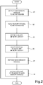
- FIG. 2 illustrates schematically, by a block diagram, a method of refresh of the memory array 2.
- the refresh method first of all comprises the step 20 of selection of a main memory module 4a-4n to be refreshed.
- the main memory module 4a is selected.
- Step 20 is followed by step 22, where the controller 8 reads the data contained in the main memory module 4a selected in step 20.
- step 22 is performed in a way transparent for the user of the nonvolatile-memory device 1, which may request reading operations by addressing any cell of any main memory module 4a-4n.
- the user requests access to the main memory module 4a simultaneously to step 22, there occurs a temporary conflict that has a negligible impact upon the reading times.
- a control signal READY assumes the logic value "0"; at the end of reading, the control signal READY assumes the logic value "1".
- the controller interface 14 has access to the control signal READY.
- step 22 If in the course of step 22 the value of the control signal READY is "0" (i.e., reading by the user is in progress), the controller interface 14 postpones the reading operation to the end of the reading operation of the user, and sets the control signal READY to the value "0" up until the end of its own reading operation. If, in the course of step 22, the value of the control signal READY is "1" (i.e., a reading access to the main memory module 4a by the user is not in progress), the controller interface 14 sets the control signal READY at the value "0" up until the end of its own reading operation so that the user may not gain access during the reading operation and thus conflicts are prevented. In any case, at the end of its own reading operation, the controller interface 14 sets the control signal READY to the logic value "1".
- Step 22 is followed by step 24, where the controller 8 writes in the auxiliary memory module 6 the data read in step 22.
- the entire contents of the main memory module 4a are copied into the auxiliary memory module 6.
- the controller 8 prevents in this step execution of operations of writing in the memory array 2.
- Step 24 is followed by step 26, where requests by the user for reading the information content of the main memory module 4a are re-addressed to the auxiliary memory module 6.
- Step 26 is followed by step 28, where the content of the main memory module 4a is physically refreshed, i.e., its content is read and overwritten.
- the user may access the auxiliary memory module 6 in order to read the content thereof, which, as has been said, corresponds to the information content of the main memory module 4a.
- the user has an uninterrupted access to the information content of the entire memory array 2, enabling use thereof for real-time applications.
- Step 28 is followed by step 30, where requests for reading the contents of the main memory module 4a, previously re-addressed to the auxiliary memory module 6 in step 26, are again addressed to the main memory module 4a.
- step 30 it is possible to return to step 20 in order to select a new main memory module 4a-4n to be refreshed.
- the controller 8 may select periodically and in a sequential way each main memory module 4a-4n according to pre-set time intervals.
- these time intervals have a duration compatible with the retention time of each memory cell of the nonvolatile-memory device 1 so as to enable an uninterrupted use of the single-ended mode of the memory array 2.
- the retention time of a memory cell is the duration that elapses between writing of a logic datum in the cell and the instant when the datum is no longer readable in so far as it is excessively degraded.
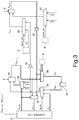
- Figure 3 shows in greater detail a portion of the nonvolatile-memory device 1 of Figure 1 , comprising the main memory module 4a, the auxiliary memory module 6, the controller 8, and the memory-array interface 16.
- the nonvolatile-memory device 1 further comprises a plurality of multiplexers designed to render transparent the refresh operation for the user of the nonvolatile-memory device 1.
- the controller 8 is further configured to generate a first control signal BUSY, a second control signal BUSY_SP, and a third control signal S COMM for controlling the plurality of multiplexers described more fully hereinafter.
- the controller 8 is further configured to receive data contained in the main memory module 4a and in the auxiliary memory module 6 via an input signal S DATA_IN .
- the signal S DATA_IN is one of the signals S MAIN_O (which carries the data contained in the main memory module 4a) and S SPARE_O (which carries the data contained in the auxiliary memory module 6) that are selected via a multiplexer 32 controlled by the first control signal BUSY.
- the multiplexer 32 is coupled to the main memory module 4a and to the auxiliary memory module 6 for receiving, respectively, the signal S MAIN_O and the signal S SPARE_O .
- the signal S SPARE_O is read following upon an operation of writing of the auxiliary memory module 6, in order to verify that the writing operation has been carried out correctly. Otherwise, according to known procedures, subsequent writing operations are carried out.
- the multiplexer 32 is coupled to the auxiliary memory module 6 via interposition of a first buffer 33 so as to reduce the propagation times associated to the auxiliary memory module 6.
- the controller 8 is further configured to: send to the main memory module 4a an output signal S DATA_OUT ' that carries data read from the main memory module 4a so as to implement step 28 of the method of Figure 2 ; and send to the auxiliary memory module 6 an output signal S DATA_OUT " that carries data read from the main memory module 4a so as to implement step 24 of the method of Figure 2 .
- the controller 8 is further configured to generate a signal S A ', containing an address of one of the memory cells of the main memory module 4a.
- the signal S A ' is supplied to an input of a multiplexer 34 controlled by the first control signal BUSY.
- the multiplexer 34 further receives a signal S INT_O from the memory-array interface 16, which contains an address for carrying out a writing operation of a conventional type of one of the memory cells of the main memory module 4a.
- the first control signal BUSY enables selection of one of the input signals S A ', S INT_O in order to generate a signal S ADDR ' at output from the multiplexer 34, according to whether it is executing the refresh method of Figure 2 or a writing operation of a conventional type.
- the signal S ADDR ' is supplied to the main memory module 4a for addressing one of the memory cells of the main memory module 4a so as to implement one of steps 24 and 28 of the refresh method of Figure 2 .
- the signal S MAIN_O at output from the main memory module 4a contains data corresponding to the data contained in the memory cell of the main memory module 4a addressed by the signal S ADDR '.
- Said signal S MAIN_O is further supplied to a multiplexer 36 controlled by the third control signal S COMM .
- the multiplexer 38 further receives at input the signal S SPARE_O from the auxiliary memory module 6 via interposition of the first buffer 33.
- the multiplexer 38 selects one of the signals S MAIN_O , S SPARE_O to generate a signal S INT_I at input to the memory-array interface 16.
- the signal S INT_I consequently contains data sent in response to reading requests from the user. These data come from the main memory module 4a or, during a refresh thereof, from the auxiliary memory module 6.
- the controller 8 is further configured to generate a signal S A ", containing an address of one of the memory cells of the auxiliary memory module 6.
- the signal S A " is supplied to an input of a multiplexer 38 controlled by the second control signal BUSY_SP.
- the multiplexer 38 further receives at input the signal S ADDR ' via interposition of a second buffer 39 so as to reduce the propagation times associated to the auxiliary memory module 6.
- the second control signal BUSY_SP enables selection of one of the input signals S A ", S ADDR ' in order to generate a signal S ADDR " at output from the multiplexer 38.
- the controller 8 is further configured to supply a multiplexer 40 with a clock signal CLK generated by a clock generator (not shown in Figure 3 ).
- the multiplexer 40 further receives at input a clock signal CLK A (generated by another clock generator not shown in Figure 3 ), which represents the standard operating clock of the main memory module 4a.
- the multiplexer 40 is controlled by the first control signal BUSY so as to generate an output signal used as clock of the main memory module 4a by selecting the signal CLK at output from the controller 8, during refresh of the main memory module 4a, and the signal CLK A , otherwise.
- the clock signal CLK at output from the controller 8 is further supplied to a multiplexer 42 controlled by the second control signal BUSY_SP.
- the multiplexer 42 further receives at input the clock signal CLK A .
- the multiplexer 42 generates an output signal used as clock of the auxiliary module 6 by selecting the signal CLK, during copying of the data of the main memory module 4a into the auxiliary memory module 6 (step 24 of the refresh method of Figure 2 ), and the signal CLK A , in the case where the user requests reading of the information content of the memory cell 4a during refresh of the main memory module 4a (step 28 of the refresh method of Figure 2 ).
- main memory modules 4b-4n are structurally equivalent to the main memory module 4a of Figure 3 , and are operatively coupled to the controller 8, to the auxiliary memory module 6, and to the memory-array interface 16 via respective multiplexers.
- each main memory module 4a-4n may be associated to a respective clock signal, for example different from the clock signal of the other main memory modules.
- each main memory module 4a-4n may operate asynchronously with respect to the others, and send respective address signals and clock signals at input to the multiplexers 38 and 42, respectively.
- each clock signal may have a frequency of its own different from the frequency of the other clock signals. Consequently, the auxiliary module 6 may be controlled for operating according to the synchronism of each clock signal and thus to the respective frequencies so as to replicate the operation of the main memory module during refresh.
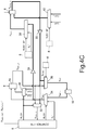
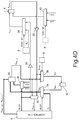
- each of Figures 4A-4E shows the portion of the nonvolatile-memory device 1 of Figure 3 during a different step of the method.
- communication lines corresponding to signals that are active in the corresponding step of the method are highlighted with the use of thick lines, where by "active signals” are meant signals that carry data during said step, signals that carry addresses to said data, and clock signals designed to time said data transport.
- Figure 4A regards step 22 of the method, where the controller 8 reads the data contained in the main memory module 4a.
- the controller 8 During Step 22, the controller 8 generates the first control signal BUSY so as to select the signals S MAIN_O , S A ', and CLK, which are thus supplied at output by the respective multiplexers 32, 34, 40. In this way, the controller 8 receives at input the signal S DATA_IN , corresponding to the datum contained in the memory cell that is addressed by the signal S A ' and is contained in the main memory module 4a. The controller 8 is configured to read in this way all the data contained in the main memory module 4a varying the address carried by the signal S A '.
- Figure 4B regards step 24 of the method, where the controller 8 writes in the auxiliary memory module 6 the data read during step 22.
- the controller 8 is configured to write in this way all the data read previously (step 22) from the main memory module 4a, varying the address carried by the signal S A ".
- Figure 4C regards step 26 of the method, and represents an operation of reading by the user of an information content of the main memory module 4a, re-addressed to the auxiliary memory module 6.
- Figure 4D regards step 28 of the method, where the content of the main memory module 4a is refreshed.
- the controller 8 generates the first control signal BUSY so as to select the signals S MAIN_O , S A ', and CLK, which are thus supplied at output by the respective multiplexers 32, 34, 40.
- step 28 Following upon reception by the controller 8 of the datum read and carried by the signal S DATA_IN , a second substep of step 28, shown in Figure 4D , is carried out, where the controller 8 continues to generate the first control signal BUSY as in the first substep, and further sends to the main memory module 4a the output signal S DATA_OUT ', containing the datum that is read in the first substep and is to be physically refreshed via overwriting.
- the controller 8 is configured to repeat the first and second substeps for each datum contained in the main memory module 4a. In particular, it is possible to carry out in a first time interval the first substep for each datum and in a second time interval the second substep. Alternatively, it is possible to carry out the second substep for one datum immediately after the first substep for the same datum, and then pass to the next datum.
- Figure 4E regards step 30 of the method and illustrates an operation of reading by the user of an information content of the main memory module 4a.
- the controller 8 controls the multiplexers 34, 36, 40 so as to select and supply at output the signals S INT_O , S MAIN_O and CLK A , respectively.
- the controller 8 controls the multiplexers 34, 36, 40 so as to select and supply at output the signals S INT_O , S MAIN_O and CLK A , respectively.
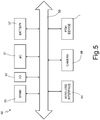
- Illustrated in Figure 5 is a portion of an electronic system 50, according to an embodiment of the present invention.
- the electronic system 50 may be used in electronic devices, such as: an electronic control unit of a vehicle; a PDA (Personal Digital Assistant); a portable or fixed computer, possibly with capacity of wireless data transfer; a mobile phone; a tablet; a smartphone; a digital audio player; a photographic or video camera; or further devices that are able to process, store, transmit and receive information.
- electronic devices such as: an electronic control unit of a vehicle; a PDA (Personal Digital Assistant); a portable or fixed computer, possibly with capacity of wireless data transfer; a mobile phone; a tablet; a smartphone; a digital audio player; a photographic or video camera; or further devices that are able to process, store, transmit and receive information.
- the electronic system 50 comprises a controller 51 (for example, provided with a microprocessor, a DSP, or a microcontroller) and the nonvolatile-memory device 1 described previously.
- the electronic system 50 comprises one or more from among an input/output device 52 (for example, provided with a keypad and a display), for input and display of data, a wireless interface 54, for example an antenna, for transmitting and receiving data through a radio-frequency wireless-communication network, and a RAM 55, all coupled through a bus 56.
- a battery 57 may be used as electrical supply source in the electronic system 50, which may further be provided with a photographic or video camera 58.
- the nonvolatile-memory device 1 may be embedded in the controller 51.
- implementation of the refresh method of the present invention enables uninterrupted use of a PCM of a differential type in single-ended mode, and consequently storage of different data in memory cells normally coupled for reading a single datum in differential mode.
- the refresh method is carried out in a way transparent for the user, which has an uninterrupted access in reading and writing to the information content of the entire nonvolatile-memory device, enabling use thereof for real-time applications.
- the refresh method may be applied to any memory of a differential type, not necessarily based upon phase-change technology.
Landscapes
- Engineering & Computer Science (AREA)
- Theoretical Computer Science (AREA)
- Physics & Mathematics (AREA)
- General Engineering & Computer Science (AREA)
- General Physics & Mathematics (AREA)
- Chemical & Material Sciences (AREA)
- Crystallography & Structural Chemistry (AREA)
- Dram (AREA)
- Debugging And Monitoring (AREA)
Abstract
Description
- The present disclosure relates to a management method of real-time access to a differential memory, a differential memory, and an electronic system including the differential memory. In particular, the differential memory is a phase-change memory. In particular, the differential memory may be operated in single-ended mode, i.e., accessing twice the number of address spaces with respect to differential memories of conventional use.
- As is known, nonvolatile phase-change memories (PCMs) represent a generation of integrated memories, where storage of information is obtained by exploiting phase-change materials, which have the property of being able to switch between phases that have electrical resistivities of considerably different value. In particular, these materials may switch between an amorphous phase, with high resistivity, and a crystalline or polycrystalline phase, with low resistivity. Consequently, in a phase-change memory cell it is possible to associate a different value of a datum stored in the cell to a respective phase of a memory element of the cell.
- For instance, it is possible to use elements of group VI of the periodic table, such as tellurium (Te), selenium (Se), or antimony (Sb), which are referred to as "chalcogenides" or "chalcogenic materials" to form phase-change memory elements. In particular, an alloy made up of germanium (Ge), antimony (Sb), and tellurium (Te), known as GST (having chemical composition Ge2Sb2Te5) currently finds wide use in such memory elements.
- Phase switching in a memory element may be obtained by locally increasing the temperature of the region of chalcogenic material, for example by causing passage of a programming electric current through resistive electrodes (generally known as "heaters") arranged in contact with the region of chalcogenic material. Said electric current, by the Joule effect, generates the temperature profile necessary for phase change. In particular, when the chalcogenic material is in the amorphous state, with high resistivity (the so-called RESET state), it is necessary to apply a first current pulse (the so-called SET pulse) of a duration and amplitude such as to enable the chalcogenic material to cool slowly. Subjected to this treatment, the chalcogenic material changes state and switches from the high-resistivity state to a low-resistivity crystalline state (the so-called SET state). Conversely, when the chalcogenic material is in the SET state, it is necessary to apply a second current pulse (the so-called RESET pulse) of large amplitude and short duration so as to cause the chalcogenic material to return into the high-resistivity amorphous state.
- In PCM circuits of a known type, reading of the datum stored in a memory cell may be carried out by applying to the memory element of chalcogenic material a voltage sufficiently low as not to cause a sensible heating thereof, and then by reading the value of the current flowing in the memory cell. Given that the current is proportional to the conductivity of the chalcogenic material, it is possible to determine in which phase the material is, and thus arrive at the datum stored in the memory cell.
- In a known way, PCMs of a differential type are typically designed according to a scheme with an array of memory cells arranged in rows (word lines) and columns (bit lines). Each memory cell is provided by a phase-change storage element and by a selector transistor, connected in series. A column decoder and a row decoder enable, on the basis of address logic signals received at input and more or less complex decoding schemes, selection of the memory cells, and in particular of the corresponding word lines and bit lines, each time addressed.
- The column decoder comprises a plurality of analog selection switches (implemented with transistors), which receive on their respective control terminals the address signals. The selection switches are arranged according to a tree structure in hierarchical levels, and their number in each hierarchical level is linked to the arrangement and size of the memory array. The selection switches, once enabled, make it possible to bring the bit line selected to a definite value of voltage and/or current, according to the operations that are to be implemented. In particular, a current path is created between a programming stage or a reading stage and the bit line selected. Said current path is defined by the series of a certain number of selection switches. In a known way, sense amplifiers carry out reading of the data stored in the memory cells, comparing the current that flows in the memory cell selected (or an electrical quantity correlated thereto) with a reference current supplied by a reference-current generator (single-ended reading) and/or by one or more reference cells, used for the entire memory array. Single-ended reading is typically used during verification that programming of the cell has occurred or during testing. During normal use of the memory, reading of a double-ended type is instead adopted, where the sense amplifiers compare the current flowing in the memory cell selected with the current flowing in a respective cell associated to the memory cell selected in the differential architecture.
- To carry out single-ended reading, one input of the sense amplifier receives the current of the memory cell that is to be read, whereas the other input of the sense amplifier receives the reference current supplied by the reference-current generator.
- Reading architectures for PCMs of a differential type afford advantages in terms of reliability in so far as the datum is stored in a redundant way and further they do not require generation of a reference current, in so far as reading is carried out by simply comparing the respective currents that flow in the cells associated to a same bit.
- In single-ended mode, it is possible to read and write independently two memory cells that are normally associated for carrying out differential reading. In effect, when it is operated in single-ended mode, each memory cell may have a value independent of the value of the other memory cells, and it is consequently possible to double the amount of data that may be stored in the PCM.
- A drawback of the PCM devices used in single-ended mode lies in the fact that in this mode the degradation over time of the logic data stored may not be compensated and, in the absence of periodic refresh operations, the associated information is lost. Instead, when PCMs are used in double-ended mode, all the logic data undergo in time common-mode degradation and, consequently, via differential reading, it is in any case possible to arrive at the desired information content, cancelling out the offset due to common-mode degradation.
- In order to prevent any loss of data in a memory cell, albeit continuing to use the single-ended mode, it is expedient to refresh the memory cell periodically. Refresh methods are known for architectures based upon fast-writing technology, such as the dynamic random-access memory (DRAM), where the time necessary for each writing operation is of the order of nanoseconds. In these methods, the datum to be refreshed is read and overwritten periodically before it gets lost.
- Conversely, in PCM technologies of a known type, the duration of a writing operation is in the region of several microseconds, typically 10 microseconds. Consequently, it would not be possible to update entire memory banks if used for applications that require real-time access to the memory (in reading and/or writing).
- The aim of the present invention is to provide a management method of real-time access to a differential memory operated in single-ended mode, a differential memory that may be operated in single-ended mode, and an electronic system including the differential memory that will be able to overcome the drawbacks of the prior art.
- According to the present invention a management method of real-time access to a differential memory operated in single-ended mode, a differential memory that may be operated in single-ended mode, and an electronic system including the differential memory are provided, as defined in the annexed claims.
- For a better understanding of the present invention, preferred embodiments thereof are now described, purely by way of non-limiting example, with reference to the attached drawings, wherein:
-
Figure 1 is a schematic illustration of a portion of a nonvolatile memory device according to one embodiment of the present invention; -
Figure 2 shows schematically, by a block diagram, a method for refresh of the nonvolatile-memory device ofFigure 1 ; -
Figure 3 shows an electrical circuit corresponding to a portion of the nonvolatile-memory device ofFigure 1 , included in the portion ofFigure 1 ; -
Figures 4A-4E show the circuit ofFigure 3 in respective steps of the method ofFigure 2 , where circuit connections of particular importance for implementation of the respective step of the method are highlighted by thick lines; and -
Figure 5 shows an electronic system that includes the nonvolatile-memory device ofFigure 1 . - Represented schematically in
Figure 1 and designated as a whole by the reference number 1 is a portion of a memory device, in particular a nonvolatile memory. According to an embodiment of the present invention, the memory 1 is of a differential type, in particular of a PCM type. The nonvolatile-memory device 1 is shown limitedly to just the parts necessary for an understanding of the present disclosure. - In particular, the nonvolatile memory device 1 comprises a
memory array 2, constituted by a plurality of "n"main memory modules 4a-4n. Eachmain memory module 4a-4n comprises afirst submodule 4a'-4n' and asecond submodule 4a"-4n". In particular, eachfirst submodule 4a'-4n' comprises a plurality of memory cells, and eachsecond submodule 4a"-4n" comprises a plurality of respective memory cells. - In a per se known manner and not shown in
Figure 1 , the plurality of first memory cells stores respective logic data of a binary type. The plurality of second memory cells corresponds, as regards number and manufacturing characteristics, to the plurality of first memory cells, and is configured to store respective logic data complementary to the logic data stored in the respective plurality of first memory cells so as to enable differential reading of said logic data. - In any case, each
main memory module 4a-4n may be used in single-ended mode, such that the logic data stored in the plurality of memory cells of eachsecond submodule 4a"-4n" are not complementary to the logic data stored in the plurality of memory cells of the respectivefirst submodule 4a'-4n', but are further information data. In this way, it is possible to double the total capacity of thememory array 2. - The nonvolatile-memory device 1 further comprises an
auxiliary memory module 6. In particular, theauxiliary memory module 6 structurally and operatively corresponds to eachmain memory module 4a-4n and is thus formed by a first submodule 6' and asecond submodule 6". In particular, the first submodule 6' comprises a plurality of memory cells, and thesecond submodule 6" comprises a plurality of respective memory cells, which may be addressed and thus may be used in single-ended mode. - In addition, the nonvolatile-memory device 1 comprises a
controller 8, operatively coupled to thememory array 2 and to theauxiliary memory module 6. Thecontroller 8 is configured to implement a method of reading and writing logic data in thememory array 2 and in theauxiliary memory module 6. - Furthermore, the nonvolatile-memory device 1 comprises a
bus 10. Thecontroller 8, themain memory modules 4a-4n, and theauxiliary memory module 6 are each coupled to thebus 10 byrespective communication lines 12a-12e so as to enable, as described in greater detail hereinafter, a transfer of data and control signals between thecontroller 8, themain memory modules 4a-4n, and theauxiliary memory module 6. - Further, the nonvolatile-memory device 1 comprises a
controller interface 14. Thecontroller interface 14 is coupled to thecontroller 8 so as to send to thecontroller 8, via acommunication line 13, logic data to be written in thememory array 2. - In addition, the nonvolatile-memory device 1 comprises a memory-
array interface 16. The memory-array interface 16 is coupled to thebus 10 via arespective communication line 12f. A user of the nonvolatile-memory device 1 may gain access, for example in reading, to the data stored in the nonvolatile-memory device 1 via the memory-array interface 16. The user is, for example, a microprocessor, a DSP, or a microcontroller. -
Figure 2 illustrates schematically, by a block diagram, a method of refresh of thememory array 2. The refresh method first of all comprises thestep 20 of selection of amain memory module 4a-4n to be refreshed. By way of example, in the course ofstep 20 themain memory module 4a is selected. -
Step 20 is followed bystep 22, where thecontroller 8 reads the data contained in themain memory module 4a selected instep 20. In particular,step 22 is performed in a way transparent for the user of the nonvolatile-memory device 1, which may request reading operations by addressing any cell of anymain memory module 4a-4n. In the case where the user requests access to themain memory module 4a simultaneously to step 22, there occurs a temporary conflict that has a negligible impact upon the reading times. In particular, when the user has access in reading to themain memory module 4a, a control signal READY assumes the logic value "0"; at the end of reading, the control signal READY assumes the logic value "1". Thecontroller interface 14 has access to the control signal READY. If in the course ofstep 22 the value of the control signal READY is "0" (i.e., reading by the user is in progress), thecontroller interface 14 postpones the reading operation to the end of the reading operation of the user, and sets the control signal READY to the value "0" up until the end of its own reading operation. If, in the course ofstep 22, the value of the control signal READY is "1" (i.e., a reading access to themain memory module 4a by the user is not in progress), thecontroller interface 14 sets the control signal READY at the value "0" up until the end of its own reading operation so that the user may not gain access during the reading operation and thus conflicts are prevented. In any case, at the end of its own reading operation, thecontroller interface 14 sets the control signal READY to the logic value "1". -
Step 22 is followed bystep 24, where thecontroller 8 writes in theauxiliary memory module 6 the data read instep 22. In particular, the entire contents of themain memory module 4a are copied into theauxiliary memory module 6. For this purpose, it could be necessary to reiterate in a number of cycles the succession ofsteps memory array 2, thecontroller 8 prevents in this step execution of operations of writing in thememory array 2. -
Step 24 is followed bystep 26, where requests by the user for reading the information content of themain memory module 4a are re-addressed to theauxiliary memory module 6. -
Step 26 is followed bystep 28, where the content of themain memory module 4a is physically refreshed, i.e., its content is read and overwritten. According to an aspect of the present invention, duringstep 28 the user may access theauxiliary memory module 6 in order to read the content thereof, which, as has been said, corresponds to the information content of themain memory module 4a. - In this way, the user has an uninterrupted access to the information content of the
entire memory array 2, enabling use thereof for real-time applications. -
Step 28 is followed bystep 30, where requests for reading the contents of themain memory module 4a, previously re-addressed to theauxiliary memory module 6 instep 26, are again addressed to themain memory module 4a. - Following upon
step 30, it is possible to return to step 20 in order to select a newmain memory module 4a-4n to be refreshed. For instance, thecontroller 8 may select periodically and in a sequential way eachmain memory module 4a-4n according to pre-set time intervals. In particular, these time intervals have a duration compatible with the retention time of each memory cell of the nonvolatile-memory device 1 so as to enable an uninterrupted use of the single-ended mode of thememory array 2. In particular, the retention time of a memory cell is the duration that elapses between writing of a logic datum in the cell and the instant when the datum is no longer readable in so far as it is excessively degraded. -
Figure 3 shows in greater detail a portion of the nonvolatile-memory device 1 ofFigure 1 , comprising themain memory module 4a, theauxiliary memory module 6, thecontroller 8, and the memory-array interface 16. In particular, the nonvolatile-memory device 1 further comprises a plurality of multiplexers designed to render transparent the refresh operation for the user of the nonvolatile-memory device 1. - The
controller 8 is further configured to generate a first control signal BUSY, a second control signal BUSY_SP, and a third control signal SCOMM for controlling the plurality of multiplexers described more fully hereinafter. - The
controller 8 is further configured to receive data contained in themain memory module 4a and in theauxiliary memory module 6 via an input signal SDATA_IN. In particular, the signal SDATA_IN is one of the signals SMAIN_O (which carries the data contained in themain memory module 4a) and SSPARE_O (which carries the data contained in the auxiliary memory module 6) that are selected via amultiplexer 32 controlled by the first control signal BUSY. For this purpose, themultiplexer 32 is coupled to themain memory module 4a and to theauxiliary memory module 6 for receiving, respectively, the signal SMAIN_O and the signal SSPARE_O. For instance, the signal SSPARE_O is read following upon an operation of writing of theauxiliary memory module 6, in order to verify that the writing operation has been carried out correctly. Otherwise, according to known procedures, subsequent writing operations are carried out. - In particular, the
multiplexer 32 is coupled to theauxiliary memory module 6 via interposition of afirst buffer 33 so as to reduce the propagation times associated to theauxiliary memory module 6. - The
controller 8 is further configured to: send to themain memory module 4a an output signal SDATA_OUT' that carries data read from themain memory module 4a so as to implementstep 28 of the method ofFigure 2 ; and send to theauxiliary memory module 6 an output signal SDATA_OUT" that carries data read from themain memory module 4a so as to implementstep 24 of the method ofFigure 2 . - The
controller 8 is further configured to generate a signal SA', containing an address of one of the memory cells of themain memory module 4a. The signal SA' is supplied to an input of amultiplexer 34 controlled by the first control signal BUSY. Themultiplexer 34 further receives a signal SINT_O from the memory-array interface 16, which contains an address for carrying out a writing operation of a conventional type of one of the memory cells of themain memory module 4a. The first control signal BUSY enables selection of one of the input signals SA', SINT_O in order to generate a signal SADDR' at output from themultiplexer 34, according to whether it is executing the refresh method ofFigure 2 or a writing operation of a conventional type. - The signal SADDR' is supplied to the
main memory module 4a for addressing one of the memory cells of themain memory module 4a so as to implement one ofsteps Figure 2 . - Consequently, the signal SMAIN_O at output from the
main memory module 4a contains data corresponding to the data contained in the memory cell of themain memory module 4a addressed by the signal SADDR'. - Said signal SMAIN_O is further supplied to a
multiplexer 36 controlled by the third control signal SCOMM. Themultiplexer 38 further receives at input the signal SSPARE_O from theauxiliary memory module 6 via interposition of thefirst buffer 33. Themultiplexer 38 selects one of the signals SMAIN_O, SSPARE_O to generate a signal SINT_I at input to the memory-array interface 16. The signal SINT_I consequently contains data sent in response to reading requests from the user. These data come from themain memory module 4a or, during a refresh thereof, from theauxiliary memory module 6. - The
controller 8 is further configured to generate a signal SA", containing an address of one of the memory cells of theauxiliary memory module 6. The signal SA" is supplied to an input of amultiplexer 38 controlled by the second control signal BUSY_SP. Themultiplexer 38 further receives at input the signal SADDR' via interposition of asecond buffer 39 so as to reduce the propagation times associated to theauxiliary memory module 6. The second control signal BUSY_SP enables selection of one of the input signals SA", SADDR' in order to generate a signal SADDR" at output from themultiplexer 38. In particular, the output signal SADDR" corresponds to the input signal SA" in the course of copying of the data of themain memory module 4a into the auxiliary memory module 6 (step 24 of the refresh method ofFigure 2 ), and to the input signal SADDR' = SINT_O in the case where the user requests reading of the information content of thememory cell 4a in the course of refresh of themain memory module 4a (step 28 of the refresh method ofFigure 2 ). - The
controller 8 is further configured to supply amultiplexer 40 with a clock signal CLK generated by a clock generator (not shown inFigure 3 ). Themultiplexer 40 further receives at input a clock signal CLKA (generated by another clock generator not shown inFigure 3 ), which represents the standard operating clock of themain memory module 4a. Themultiplexer 40 is controlled by the first control signal BUSY so as to generate an output signal used as clock of themain memory module 4a by selecting the signal CLK at output from thecontroller 8, during refresh of themain memory module 4a, and the signal CLKA, otherwise. - The clock signal CLK at output from the
controller 8 is further supplied to amultiplexer 42 controlled by the second control signal BUSY_SP. Themultiplexer 42 further receives at input the clock signal CLKA. Themultiplexer 42 generates an output signal used as clock of theauxiliary module 6 by selecting the signal CLK, during copying of the data of themain memory module 4a into the auxiliary memory module 6 (step 24 of the refresh method ofFigure 2 ), and the signal CLKA, in the case where the user requests reading of the information content of thememory cell 4a during refresh of themain memory module 4a (step 28 of the refresh method ofFigure 2 ). - It is evident that the other
main memory modules 4b-4n are structurally equivalent to themain memory module 4a ofFigure 3 , and are operatively coupled to thecontroller 8, to theauxiliary memory module 6, and to the memory-array interface 16 via respective multiplexers. Furthermore, eachmain memory module 4a-4n may be associated to a respective clock signal, for example different from the clock signal of the other main memory modules. In other words, eachmain memory module 4a-4n may operate asynchronously with respect to the others, and send respective address signals and clock signals at input to themultiplexers - In particular, each clock signal may have a frequency of its own different from the frequency of the other clock signals. Consequently, the
auxiliary module 6 may be controlled for operating according to the synchronism of each clock signal and thus to the respective frequencies so as to replicate the operation of the main memory module during refresh. - In order to describe in greater detail some steps of the refresh method of
Figure 2 , each ofFigures 4A-4E shows the portion of the nonvolatile-memory device 1 ofFigure 3 during a different step of the method. In each ofFigures 4A-4E , communication lines corresponding to signals that are active in the corresponding step of the method are highlighted with the use of thick lines, where by "active signals" are meant signals that carry data during said step, signals that carry addresses to said data, and clock signals designed to time said data transport. - In particular,
Figure 4A regardsstep 22 of the method, where thecontroller 8 reads the data contained in themain memory module 4a. - During
Step 22, thecontroller 8 generates the first control signal BUSY so as to select the signals SMAIN_O, SA', and CLK, which are thus supplied at output by therespective multiplexers controller 8 receives at input the signal SDATA_IN, corresponding to the datum contained in the memory cell that is addressed by the signal SA' and is contained in themain memory module 4a. Thecontroller 8 is configured to read in this way all the data contained in themain memory module 4a varying the address carried by the signal SA'. -
Figure 4B regardsstep 24 of the method, where thecontroller 8 writes in theauxiliary memory module 6 the data read duringstep 22. - During
step 24, thecontroller 8 generates the second control signal BUSY_SP so as to select the signals SA" and CLK, which are thus supplied at output by therespective multiplexers controller 8 sends to theauxiliary memory module 6 the output signal SDATA_OUT", containing data to be written in the memory cell of theauxiliary memory module 6 addressed by the signal SADDR" = SA". Thecontroller 8 is configured to write in this way all the data read previously (step 22) from themain memory module 4a, varying the address carried by the signal SA". -
Figure 4C regards step 26 of the method, and represents an operation of reading by the user of an information content of themain memory module 4a, re-addressed to theauxiliary memory module 6. - In the time interval that elapses from execution of
step 26 to start ofstep 30, thecontroller 8 generates the second control signal BUSY_SP so as to select the signals SINT_O, SADDR' and CLKA, which are thus supplied at output by therespective multiplexers controller 8 generates the third control signal SCOMM so as to select the signal SSPARE_O, supplied at output by themultiplexer 36. In this way, whenever in said time interval the user requests reading of the information content of themain memory module 4a associated to the memory cell addressed by the signal SINT_O, the datum contained in the memory cell of theauxiliary memory module 6 addressed by the signal SADDR" = SADDR' = SINT_O is read. Said datum, supplied at output by theauxiliary memory module 6 via the signal SSPARE_O, is thus sent to the memory-array interface 16 via the signal SINT_I. -
Figure 4D regards step 28 of the method, where the content of themain memory module 4a is refreshed. - In the course of
step 28, in a first substep (not illustrated graphically inFigure 4D ), thecontroller 8 reads the datum of the memory cell of themain memory module 4a addressed by the signal SADDR' = SA'. For this purpose, as already shown inFigure 4A forstep 22, thecontroller 8 generates the first control signal BUSY so as to select the signals SMAIN_O, SA', and CLK, which are thus supplied at output by therespective multiplexers - Following upon reception by the
controller 8 of the datum read and carried by the signal SDATA_IN, a second substep ofstep 28, shown inFigure 4D , is carried out, where thecontroller 8 continues to generate the first control signal BUSY as in the first substep, and further sends to themain memory module 4a the output signal SDATA_OUT', containing the datum that is read in the first substep and is to be physically refreshed via overwriting. - The
controller 8 is configured to repeat the first and second substeps for each datum contained in themain memory module 4a. In particular, it is possible to carry out in a first time interval the first substep for each datum and in a second time interval the second substep. Alternatively, it is possible to carry out the second substep for one datum immediately after the first substep for the same datum, and then pass to the next datum. -
Figure 4E regards step 30 of the method and illustrates an operation of reading by the user of an information content of themain memory module 4a. - In a time interval that elapses from execution of
step 30 up to execution ofstep 26 of a subsequent iteration of the refresh method ofFigure 2 , thecontroller 8 controls themultiplexers main memory module 4a associated to the memory cell addressed by the signal SINT_O, the datum contained in the memory cell of themain memory module 4a addressed by the signal SADDR' = SINT_O is read. This datum, supplied at output by themain memory module 4a via the signal SMAIN_O is thus sent to the memory-array interface 16 via the signal SINT_I. - Illustrated in
Figure 5 is a portion of anelectronic system 50, according to an embodiment of the present invention. Theelectronic system 50 may be used in electronic devices, such as: an electronic control unit of a vehicle; a PDA (Personal Digital Assistant); a portable or fixed computer, possibly with capacity of wireless data transfer; a mobile phone; a tablet; a smartphone; a digital audio player; a photographic or video camera; or further devices that are able to process, store, transmit and receive information. - In detail, the
electronic system 50 comprises a controller 51 (for example, provided with a microprocessor, a DSP, or a microcontroller) and the nonvolatile-memory device 1 described previously. Optionally, theelectronic system 50 comprises one or more from among an input/output device 52 (for example, provided with a keypad and a display), for input and display of data, awireless interface 54, for example an antenna, for transmitting and receiving data through a radio-frequency wireless-communication network, and aRAM 55, all coupled through abus 56. Abattery 57 may be used as electrical supply source in theelectronic system 50, which may further be provided with a photographic orvideo camera 58. - According to a further embodiment not illustrated in the figures, the nonvolatile-memory device 1 may be embedded in the
controller 51. - From an examination of the characteristics of the invention described and illustrated herein, the advantages that it affords are evident.
- In particular, implementation of the refresh method of the present invention enables uninterrupted use of a PCM of a differential type in single-ended mode, and consequently storage of different data in memory cells normally coupled for reading a single datum in differential mode.
- In this way, it is possible to increase the total capacity of a PCM designed for operating in differential mode, without appreciably increasing the size and costs thereof.
- Furthermore, the refresh method is carried out in a way transparent for the user, which has an uninterrupted access in reading and writing to the information content of the entire nonvolatile-memory device, enabling use thereof for real-time applications.
- Finally, it is clear that modifications and variations may be made to the disclosure described and illustrated herein, without thereby departing from the scope of the present invention, as defined in the annexed claims.
- For instance, the refresh method may be applied to any memory of a differential type, not necessarily based upon phase-change technology.
Claims (17)
- A management method of real-time access to logic data stored in a differential memory (1) carried out in single-ended mode and comprising a first main memory module (4a), which stores first logic data to be refreshed, and an auxiliary memory module (6), said method comprising the steps of:a- storing (24) second logic data in the auxiliary memory module (6), copying the first logic data;b- refreshing (28) the first logic data; andc- fetching (26, 30), in response to a request for reading the first logic data, the second logic data during the step of refreshing (28) the first logic data, and fetching the first logic data, otherwise.
- A method according to claim 1, wherein the step of refreshing (28) the first logic data is carried out following upon the step of storing (24) the second logic data.
- A method according to claim 1 or claim 2, further comprising, following upon the step of fetching (26, 30) the first logic data or the second logic data, supplying the first logic data or the second logic data that have been fetched to a user of said differential memory (1).
- A method according to any one of the preceding claims, wherein the refresh step (28) comprises reading the first logic data from the first main memory module (4a) and rewriting said first logic data into the first main memory module (4a).
- A method according to any one of the preceding claims, wherein the differential memory (1) further comprises a second main memory module (4b) that stores third logic data to be refreshed, said method further comprising the steps of:- storing (24) fourth logic data in the auxiliary memory module (6), copying the third logic data;- refreshing (28) the third logic data; and- fetching (26, 30), in response to a request for reading the third logic data, the fourth logic data during the step of refreshing (28) the third logic data, and fetching the third logic data, otherwise.
- A method according to claim 5, wherein the first main memory module (4a) is synchronised to a first clock signal (CLKA) having a first frequency, and the second main memory module (4b) is synchronised to a second clock signal having a second frequency different from the first frequency, the method further comprising the steps of:- causing the auxiliary memory module (6) to operate according to the synchronism of the first clock signal (CLKA) during fetching of the second logic data; and- causing the auxiliary memory module (6) to operate according to the synchronism of the second clock signal during fetching of the fourth logic data.
- A method according to any one of the preceding claims, further comprising repeating steps a to c at regular intervals having a duration shorter than a retention time of the first logic data.
- A method according to any one of the preceding claims, wherein the differential memory (1) is a phase-change memory.
- A differential memory (1) that may be operated in single-ended mode comprising:- a first main memory module (4a) that stores first logic data to be refreshed;- an auxiliary memory module (6); and- a controller (8) configured to:a- control storage (24) of second logic data in the auxiliary memory module (6), copying the first logic data;b- refresh (28) the first logic data;c- fetch (26, 30), in response to a request for reading the first logic data, the second logic data during the step of refreshing (28) the first logic data, and fetching the first logic data, otherwise.
- A memory according to claim 9, wherein the controller (8) is further configured to carry out the operation of refreshing (28) the first logic data subsequent to storage (24) of the second logic data.
- A memory according to claim 9 or claim 10, further comprising an interface (16) for input and output of logic data, the controller (8) being further configured to supply the first logic data or the second logic data that have been fetched to said interface (16).
- A memory according to any one of claims 9 to 11, wherein the controller (8) is further configured to carry out the refresh operation (28) by reading the first logic data from the first main memory module (4a) and rewrite said first logic data into the first main memory module (4a) .
- A memory according to any one of claims 9 to 12, further comprising a second main memory module (4b) that stores third logic data to be refreshed,
the controller (8) being further organised for:- controlling storage (24) of fourth logic data in the auxiliary memory module (6), copying the third logic data;- refreshing (28) the third logic data; and- fetching (26, 30), in response to a request for reading the third logic data, the fourth logic data during the step of refreshing (28) the third logic data, and fetching the third logic data, otherwise. - A memory according to claim 13, wherein the first main memory module (4a) is synchronised to a first clock signal (CLKA) having a first frequency, and the second main memory module (4b) is synchronised to a second clock signal having a second frequency different from the first frequency,
the memory further comprising a multiplexer (42) having a first input that receives the first clock signal (CLKA), a second input that receives the second clock signal, and an output coupled to the auxiliary memory module (6),
the controller (8) being further configured to:- control the multiplexer (42) so as to couple the first input to the output during fetching of the second logic data so that the auxiliary memory module (6) will operate according to the synchronism of the first clock signal (CLKA); and- control the multiplexer (42) so as to couple the second input to the output during fetching of the fourth logic data so that the auxiliary memory module (6) will operate according to the synchronism of the second clock signal. - A memory according to any one of claims 9 to 14, wherein the controller (8) is further configured to repeat steps a to c at regular intervals having a duration shorter than a retention time of the first logic data.
- A memory according to any one of claims 9 to 15, wherein the differential memory is a phase-change memory.
- An electronic system (50) comprising a differential memory (1) according to any one of claims 9 to 16, chosen from one of the following: an electronic control unit of a vehicle, a personal digital assistant (PDA); a notebook; a mobile phone; a smartphone; a tablet; a digital audio player; a photographic camera or video camera; or further devices that are able to process, store, transmit, and/or receive information.
Applications Claiming Priority (1)
| Application Number | Priority Date | Filing Date | Title |
|---|---|---|---|
| IT201800000581A IT201800000581A1 (en) | 2018-01-05 | 2018-01-05 | METHOD OF MANAGING REAL-TIME ACCESS TO A DIFFERENTIAL MEMORY, DIFFERENTIAL MEMORY AND ELECTRONIC SYSTEM INCLUDING THE DIFFERENTIAL MEMORY |
Publications (2)
| Publication Number | Publication Date |
|---|---|
| EP3509067A1 true EP3509067A1 (en) | 2019-07-10 |
| EP3509067B1 EP3509067B1 (en) | 2021-03-03 |
Family
ID=61873830
Family Applications (1)
| Application Number | Title | Priority Date | Filing Date |
|---|---|---|---|
| EP19150401.8A Active EP3509067B1 (en) | 2018-01-05 | 2019-01-04 | Management method of real-time access to a differential memory, differential memory, and electronic system including the differential memory |
Country Status (4)
| Country | Link |
|---|---|
| US (1) | US10811093B2 (en) |
| EP (1) | EP3509067B1 (en) |
| CN (1) | CN110010181B (en) |
| IT (1) | IT201800000581A1 (en) |
Families Citing this family (1)
| Publication number | Priority date | Publication date | Assignee | Title |
|---|---|---|---|---|
| US11256442B2 (en) | 2018-01-05 | 2022-02-22 | Stmicroelectronics S.R.L. | Real-time update method for a differential memory, differential memory and electronic system |
Citations (2)
| Publication number | Priority date | Publication date | Assignee | Title |
|---|---|---|---|---|
| US5950224A (en) * | 1996-02-20 | 1999-09-07 | Sgs-Thomas Microelectronics S.A. | Electrically modifiable non-volatile memory circuit having means for autonomous refreshing dependent upon on periodic clock pulses |
| US20080170431A1 (en) * | 2007-01-12 | 2008-07-17 | Industrial Technology Research Institute | Driving method and system for a phase change memory |
Family Cites Families (11)
| Publication number | Priority date | Publication date | Assignee | Title |
|---|---|---|---|---|
| US4292676A (en) * | 1978-11-15 | 1981-09-29 | Lockheed Electronics Co., Inc. | Refresh cycle minimizer in a dynamic semiconductor memory |
| US4819154A (en) * | 1982-12-09 | 1989-04-04 | Sequoia Systems, Inc. | Memory back up system with one cache memory and two physically separated main memories |
| US6151236A (en) * | 2000-02-29 | 2000-11-21 | Enhanced Memory Systems, Inc. | Enhanced bus turnaround integrated circuit dynamic random access memory device |
| JP4940824B2 (en) | 2006-08-18 | 2012-05-30 | 富士通セミコンダクター株式会社 | Nonvolatile semiconductor memory |
| WO2008058101A2 (en) | 2006-11-07 | 2008-05-15 | Sandisk Corporation | Memory controllers for performing resilient firmware upgrades to a functioning memory |
| IT1403899B1 (en) * | 2010-12-30 | 2013-11-08 | Incard Sa | METHOD AND SYSTEM TO CHECK THE LOSS OF RELIABILITY OF A NON-VOLATILE MEMORY |
| WO2015106162A1 (en) * | 2014-01-09 | 2015-07-16 | SanDisk Technologies, Inc. | Selective copyback for on die buffered non-volatile memory |
| US20150339069A1 (en) | 2014-05-22 | 2015-11-26 | Kabushiki Kaisha Toshiba | Memory system and method |
| US10120674B2 (en) | 2015-06-02 | 2018-11-06 | Texas Instruments Incorporated | Ferroelectric memory expansion for firmware updates |
| DE102016214879A1 (en) | 2016-08-10 | 2018-02-15 | Robert Bosch Gmbh | Method and device for operating a memory |
| US10269420B2 (en) * | 2016-12-13 | 2019-04-23 | Taiwan Semiconductor Manufacturing Co., Ltd. | Memory with symmetric read current profile and read method thereof |
-
2018
- 2018-01-05 IT IT201800000581A patent/IT201800000581A1/en unknown
- 2018-12-19 US US16/225,492 patent/US10811093B2/en active Active
-
2019
- 2019-01-04 EP EP19150401.8A patent/EP3509067B1/en active Active
- 2019-01-07 CN CN201910013551.4A patent/CN110010181B/en active Active
Patent Citations (2)
| Publication number | Priority date | Publication date | Assignee | Title |
|---|---|---|---|---|
| US5950224A (en) * | 1996-02-20 | 1999-09-07 | Sgs-Thomas Microelectronics S.A. | Electrically modifiable non-volatile memory circuit having means for autonomous refreshing dependent upon on periodic clock pulses |
| US20080170431A1 (en) * | 2007-01-12 | 2008-07-17 | Industrial Technology Research Institute | Driving method and system for a phase change memory |
Also Published As
| Publication number | Publication date |
|---|---|
| US10811093B2 (en) | 2020-10-20 |
| EP3509067B1 (en) | 2021-03-03 |
| IT201800000581A1 (en) | 2019-07-05 |
| US20190214083A1 (en) | 2019-07-11 |
| CN110010181B (en) | 2023-04-07 |
| CN110010181A (en) | 2019-07-12 |
Similar Documents
| Publication | Publication Date | Title |
|---|---|---|
| US20230110946A1 (en) | Counter-based methods and systems for accessing memory cells | |
| WO2008032394A1 (en) | Semiconductor device | |
| EP3509066B1 (en) | Real-time update method of a differential memory with continuous reading accessibility, differential memory and electronic system | |
| EP3509065A1 (en) | A device for switching between different reading modes of a non-volatile memory and method for reading a non-volatile memory | |
| US11645004B2 (en) | Real-time update method for a differential memory, differential memory and electronic system | |
| JP2006079609A (en) | Method and apparatus using phase change memory as a replacement for buffered flash memory | |
| JP5518441B2 (en) | Low power access method for phase change memory device | |
| EP3509067B1 (en) | Management method of real-time access to a differential memory, differential memory, and electronic system including the differential memory | |
| US11049561B2 (en) | Method for programming a phase-change memory device of differential type, memory device, and electronic system | |
| US10186317B2 (en) | Phase change memory device and method of operation | |
| US11756614B2 (en) | Phase change memory device, system including the memory device, and method for operating the memory device | |
| US11355191B2 (en) | Method for programming a phase-change memory device of differential type, phase-change memory device, and electronic system | |
| EP1733398A4 (en) | Circuit for accessing a chalcogenide memory array | |
| TW202340961A (en) | Memory device and memory control method | |
| US8760938B2 (en) | Writing bit alterable memories |
Legal Events
| Date | Code | Title | Description |
|---|---|---|---|
| PUAI | Public reference made under article 153(3) epc to a published international application that has entered the european phase |
Free format text: ORIGINAL CODE: 0009012 |
|
| STAA | Information on the status of an ep patent application or granted ep patent |
Free format text: STATUS: THE APPLICATION HAS BEEN PUBLISHED |
|
| AK | Designated contracting states |
Kind code of ref document: A1 Designated state(s): AL AT BE BG CH CY CZ DE DK EE ES FI FR GB GR HR HU IE IS IT LI LT LU LV MC MK MT NL NO PL PT RO RS SE SI SK SM TR |
|
| AX | Request for extension of the european patent |
Extension state: BA ME |
|
| STAA | Information on the status of an ep patent application or granted ep patent |
Free format text: STATUS: REQUEST FOR EXAMINATION WAS MADE |
|
| STAA | Information on the status of an ep patent application or granted ep patent |
Free format text: STATUS: EXAMINATION IS IN PROGRESS |
|
| 17P | Request for examination filed |
Effective date: 20191114 |
|
| RBV | Designated contracting states (corrected) |
Designated state(s): AL AT BE BG CH CY CZ DE DK EE ES FI FR GB GR HR HU IE IS IT LI LT LU LV MC MK MT NL NO PL PT RO RS SE SI SK SM TR |
|
| 17Q | First examination report despatched |
Effective date: 20200107 |
|
| GRAP | Despatch of communication of intention to grant a patent |
Free format text: ORIGINAL CODE: EPIDOSNIGR1 |
|
| STAA | Information on the status of an ep patent application or granted ep patent |
Free format text: STATUS: GRANT OF PATENT IS INTENDED |
|
| INTG | Intention to grant announced |
Effective date: 20200928 |
|
| GRAS | Grant fee paid |
Free format text: ORIGINAL CODE: EPIDOSNIGR3 |
|
| GRAA | (expected) grant |
Free format text: ORIGINAL CODE: 0009210 |
|
| STAA | Information on the status of an ep patent application or granted ep patent |
Free format text: STATUS: THE PATENT HAS BEEN GRANTED |
|
| AK | Designated contracting states |
Kind code of ref document: B1 Designated state(s): AL AT BE BG CH CY CZ DE DK EE ES FI FR GB GR HR HU IE IS IT LI LT LU LV MC MK MT NL NO PL PT RO RS SE SI SK SM TR |
|
| REG | Reference to a national code |
Ref country code: GB Ref legal event code: FG4D |
|
| REG | Reference to a national code |
Ref country code: CH Ref legal event code: EP Ref country code: AT Ref legal event code: REF Ref document number: 1368079 Country of ref document: AT Kind code of ref document: T Effective date: 20210315 |
|
| REG | Reference to a national code |
Ref country code: DE Ref legal event code: R096 Ref document number: 602019002809 Country of ref document: DE |
|
| REG | Reference to a national code |
Ref country code: IE Ref legal event code: FG4D |
|
| REG | Reference to a national code |
Ref country code: LT Ref legal event code: MG9D |
|
| PG25 | Lapsed in a contracting state [announced via postgrant information from national office to epo] |
Ref country code: HR Free format text: LAPSE BECAUSE OF FAILURE TO SUBMIT A TRANSLATION OF THE DESCRIPTION OR TO PAY THE FEE WITHIN THE PRESCRIBED TIME-LIMIT Effective date: 20210303 Ref country code: GR Free format text: LAPSE BECAUSE OF FAILURE TO SUBMIT A TRANSLATION OF THE DESCRIPTION OR TO PAY THE FEE WITHIN THE PRESCRIBED TIME-LIMIT Effective date: 20210604 Ref country code: FI Free format text: LAPSE BECAUSE OF FAILURE TO SUBMIT A TRANSLATION OF THE DESCRIPTION OR TO PAY THE FEE WITHIN THE PRESCRIBED TIME-LIMIT Effective date: 20210303 Ref country code: BG Free format text: LAPSE BECAUSE OF FAILURE TO SUBMIT A TRANSLATION OF THE DESCRIPTION OR TO PAY THE FEE WITHIN THE PRESCRIBED TIME-LIMIT Effective date: 20210603 Ref country code: LT Free format text: LAPSE BECAUSE OF FAILURE TO SUBMIT A TRANSLATION OF THE DESCRIPTION OR TO PAY THE FEE WITHIN THE PRESCRIBED TIME-LIMIT Effective date: 20210303 Ref country code: NO Free format text: LAPSE BECAUSE OF FAILURE TO SUBMIT A TRANSLATION OF THE DESCRIPTION OR TO PAY THE FEE WITHIN THE PRESCRIBED TIME-LIMIT Effective date: 20210603 |
|
| REG | Reference to a national code |
Ref country code: NL Ref legal event code: MP Effective date: 20210303 |
|
| REG | Reference to a national code |
Ref country code: AT Ref legal event code: MK05 Ref document number: 1368079 Country of ref document: AT Kind code of ref document: T Effective date: 20210303 |
|
| PG25 | Lapsed in a contracting state [announced via postgrant information from national office to epo] |
Ref country code: SE Free format text: LAPSE BECAUSE OF FAILURE TO SUBMIT A TRANSLATION OF THE DESCRIPTION OR TO PAY THE FEE WITHIN THE PRESCRIBED TIME-LIMIT Effective date: 20210303 Ref country code: RS Free format text: LAPSE BECAUSE OF FAILURE TO SUBMIT A TRANSLATION OF THE DESCRIPTION OR TO PAY THE FEE WITHIN THE PRESCRIBED TIME-LIMIT Effective date: 20210303 Ref country code: LV Free format text: LAPSE BECAUSE OF FAILURE TO SUBMIT A TRANSLATION OF THE DESCRIPTION OR TO PAY THE FEE WITHIN THE PRESCRIBED TIME-LIMIT Effective date: 20210303 Ref country code: PL Free format text: LAPSE BECAUSE OF FAILURE TO SUBMIT A TRANSLATION OF THE DESCRIPTION OR TO PAY THE FEE WITHIN THE PRESCRIBED TIME-LIMIT Effective date: 20210303 |
|
| PG25 | Lapsed in a contracting state [announced via postgrant information from national office to epo] |
Ref country code: NL Free format text: LAPSE BECAUSE OF FAILURE TO SUBMIT A TRANSLATION OF THE DESCRIPTION OR TO PAY THE FEE WITHIN THE PRESCRIBED TIME-LIMIT Effective date: 20210303 |
|
| PG25 | Lapsed in a contracting state [announced via postgrant information from national office to epo] |
Ref country code: SM Free format text: LAPSE BECAUSE OF FAILURE TO SUBMIT A TRANSLATION OF THE DESCRIPTION OR TO PAY THE FEE WITHIN THE PRESCRIBED TIME-LIMIT Effective date: 20210303 Ref country code: AT Free format text: LAPSE BECAUSE OF FAILURE TO SUBMIT A TRANSLATION OF THE DESCRIPTION OR TO PAY THE FEE WITHIN THE PRESCRIBED TIME-LIMIT Effective date: 20210303 Ref country code: CZ Free format text: LAPSE BECAUSE OF FAILURE TO SUBMIT A TRANSLATION OF THE DESCRIPTION OR TO PAY THE FEE WITHIN THE PRESCRIBED TIME-LIMIT Effective date: 20210303 Ref country code: EE Free format text: LAPSE BECAUSE OF FAILURE TO SUBMIT A TRANSLATION OF THE DESCRIPTION OR TO PAY THE FEE WITHIN THE PRESCRIBED TIME-LIMIT Effective date: 20210303 |
|
| PG25 | Lapsed in a contracting state [announced via postgrant information from national office to epo] |
Ref country code: PT Free format text: LAPSE BECAUSE OF FAILURE TO SUBMIT A TRANSLATION OF THE DESCRIPTION OR TO PAY THE FEE WITHIN THE PRESCRIBED TIME-LIMIT Effective date: 20210705 Ref country code: RO Free format text: LAPSE BECAUSE OF FAILURE TO SUBMIT A TRANSLATION OF THE DESCRIPTION OR TO PAY THE FEE WITHIN THE PRESCRIBED TIME-LIMIT Effective date: 20210303 Ref country code: SK Free format text: LAPSE BECAUSE OF FAILURE TO SUBMIT A TRANSLATION OF THE DESCRIPTION OR TO PAY THE FEE WITHIN THE PRESCRIBED TIME-LIMIT Effective date: 20210303 Ref country code: IS Free format text: LAPSE BECAUSE OF FAILURE TO SUBMIT A TRANSLATION OF THE DESCRIPTION OR TO PAY THE FEE WITHIN THE PRESCRIBED TIME-LIMIT Effective date: 20210703 |
|
| REG | Reference to a national code |
Ref country code: DE Ref legal event code: R097 Ref document number: 602019002809 Country of ref document: DE |
|
| PLBE | No opposition filed within time limit |
Free format text: ORIGINAL CODE: 0009261 |
|
| STAA | Information on the status of an ep patent application or granted ep patent |
Free format text: STATUS: NO OPPOSITION FILED WITHIN TIME LIMIT |
|
| PG25 | Lapsed in a contracting state [announced via postgrant information from national office to epo] |
Ref country code: ES Free format text: LAPSE BECAUSE OF FAILURE TO SUBMIT A TRANSLATION OF THE DESCRIPTION OR TO PAY THE FEE WITHIN THE PRESCRIBED TIME-LIMIT Effective date: 20210303 Ref country code: AL Free format text: LAPSE BECAUSE OF FAILURE TO SUBMIT A TRANSLATION OF THE DESCRIPTION OR TO PAY THE FEE WITHIN THE PRESCRIBED TIME-LIMIT Effective date: 20210303 Ref country code: DK Free format text: LAPSE BECAUSE OF FAILURE TO SUBMIT A TRANSLATION OF THE DESCRIPTION OR TO PAY THE FEE WITHIN THE PRESCRIBED TIME-LIMIT Effective date: 20210303 |
|
| 26N | No opposition filed |
Effective date: 20211206 |
|
| PG25 | Lapsed in a contracting state [announced via postgrant information from national office to epo] |
Ref country code: SI Free format text: LAPSE BECAUSE OF FAILURE TO SUBMIT A TRANSLATION OF THE DESCRIPTION OR TO PAY THE FEE WITHIN THE PRESCRIBED TIME-LIMIT Effective date: 20210303 |
|
| PG25 | Lapsed in a contracting state [announced via postgrant information from national office to epo] |
Ref country code: IT Free format text: LAPSE BECAUSE OF FAILURE TO SUBMIT A TRANSLATION OF THE DESCRIPTION OR TO PAY THE FEE WITHIN THE PRESCRIBED TIME-LIMIT Effective date: 20210303 |
|
| PG25 | Lapsed in a contracting state [announced via postgrant information from national office to epo] |
Ref country code: IS Free format text: LAPSE BECAUSE OF FAILURE TO SUBMIT A TRANSLATION OF THE DESCRIPTION OR TO PAY THE FEE WITHIN THE PRESCRIBED TIME-LIMIT Effective date: 20210703 |
|
| PG25 | Lapsed in a contracting state [announced via postgrant information from national office to epo] |
Ref country code: MC Free format text: LAPSE BECAUSE OF FAILURE TO SUBMIT A TRANSLATION OF THE DESCRIPTION OR TO PAY THE FEE WITHIN THE PRESCRIBED TIME-LIMIT Effective date: 20210303 |
|
| REG | Reference to a national code |
Ref country code: CH Ref legal event code: PL |
|
| REG | Reference to a national code |
Ref country code: BE Ref legal event code: MM Effective date: 20220131 |
|
| PG25 | Lapsed in a contracting state [announced via postgrant information from national office to epo] |
Ref country code: LU Free format text: LAPSE BECAUSE OF NON-PAYMENT OF DUE FEES Effective date: 20220104 |
|
| PG25 | Lapsed in a contracting state [announced via postgrant information from national office to epo] |
Ref country code: FR Free format text: LAPSE BECAUSE OF NON-PAYMENT OF DUE FEES Effective date: 20220131 Ref country code: BE Free format text: LAPSE BECAUSE OF NON-PAYMENT OF DUE FEES Effective date: 20220131 |
|
| PG25 | Lapsed in a contracting state [announced via postgrant information from national office to epo] |
Ref country code: LI Free format text: LAPSE BECAUSE OF NON-PAYMENT OF DUE FEES Effective date: 20220131 Ref country code: CH Free format text: LAPSE BECAUSE OF NON-PAYMENT OF DUE FEES Effective date: 20220131 |
|
| PG25 | Lapsed in a contracting state [announced via postgrant information from national office to epo] |
Ref country code: IE Free format text: LAPSE BECAUSE OF NON-PAYMENT OF DUE FEES Effective date: 20220104 |
|
| GBPC | Gb: european patent ceased through non-payment of renewal fee |
Effective date: 20230104 |
|
| PG25 | Lapsed in a contracting state [announced via postgrant information from national office to epo] |
Ref country code: GB Free format text: LAPSE BECAUSE OF NON-PAYMENT OF DUE FEES Effective date: 20230104 |
|
| PG25 | Lapsed in a contracting state [announced via postgrant information from national office to epo] |
Ref country code: HU Free format text: LAPSE BECAUSE OF FAILURE TO SUBMIT A TRANSLATION OF THE DESCRIPTION OR TO PAY THE FEE WITHIN THE PRESCRIBED TIME-LIMIT; INVALID AB INITIO Effective date: 20190104 |
|
| PG25 | Lapsed in a contracting state [announced via postgrant information from national office to epo] |
Ref country code: MK Free format text: LAPSE BECAUSE OF FAILURE TO SUBMIT A TRANSLATION OF THE DESCRIPTION OR TO PAY THE FEE WITHIN THE PRESCRIBED TIME-LIMIT Effective date: 20210303 Ref country code: CY Free format text: LAPSE BECAUSE OF FAILURE TO SUBMIT A TRANSLATION OF THE DESCRIPTION OR TO PAY THE FEE WITHIN THE PRESCRIBED TIME-LIMIT Effective date: 20210303 |
|
| PG25 | Lapsed in a contracting state [announced via postgrant information from national office to epo] |
Ref country code: TR Free format text: LAPSE BECAUSE OF FAILURE TO SUBMIT A TRANSLATION OF THE DESCRIPTION OR TO PAY THE FEE WITHIN THE PRESCRIBED TIME-LIMIT Effective date: 20210303 |
|
| PG25 | Lapsed in a contracting state [announced via postgrant information from national office to epo] |
Ref country code: MT Free format text: LAPSE BECAUSE OF FAILURE TO SUBMIT A TRANSLATION OF THE DESCRIPTION OR TO PAY THE FEE WITHIN THE PRESCRIBED TIME-LIMIT Effective date: 20210303 |
|
| PGFP | Annual fee paid to national office [announced via postgrant information from national office to epo] |
Ref country code: DE Payment date: 20251217 Year of fee payment: 8 |