EP3508979A2 - Semiconductor device - Google Patents
Semiconductor device Download PDFInfo
- Publication number
- EP3508979A2 EP3508979A2 EP18188636.7A EP18188636A EP3508979A2 EP 3508979 A2 EP3508979 A2 EP 3508979A2 EP 18188636 A EP18188636 A EP 18188636A EP 3508979 A2 EP3508979 A2 EP 3508979A2
- Authority
- EP
- European Patent Office
- Prior art keywords
- address
- circuit
- memory
- error
- access
- Prior art date
- Legal status (The legal status is an assumption and is not a legal conclusion. Google has not performed a legal analysis and makes no representation as to the accuracy of the status listed.)
- Granted
Links
Images


Classifications
-
- G—PHYSICS
- G11—INFORMATION STORAGE
- G11C—STATIC STORES
- G11C29/00—Checking stores for correct operation ; Subsequent repair; Testing stores during standby or offline operation
- G11C29/04—Detection or location of defective memory elements, e.g. cell constructio details, timing of test signals
- G11C29/08—Functional testing, e.g. testing during refresh, power-on self testing [POST] or distributed testing
- G11C29/12—Built-in arrangements for testing, e.g. built-in self testing [BIST] or interconnection details
- G11C29/18—Address generation devices; Devices for accessing memories, e.g. details of addressing circuits
-
- G—PHYSICS
- G06—COMPUTING OR CALCULATING; COUNTING
- G06F—ELECTRIC DIGITAL DATA PROCESSING
- G06F11/00—Error detection; Error correction; Monitoring
- G06F11/07—Responding to the occurrence of a fault, e.g. fault tolerance
- G06F11/08—Error detection or correction by redundancy in data representation, e.g. by using checking codes
- G06F11/10—Adding special bits or symbols to the coded information, e.g. parity check, casting out 9's or 11's
- G06F11/1008—Adding special bits or symbols to the coded information, e.g. parity check, casting out 9's or 11's in individual solid state devices
- G06F11/1048—Adding special bits or symbols to the coded information, e.g. parity check, casting out 9's or 11's in individual solid state devices using arrangements adapted for a specific error detection or correction feature
-
- G—PHYSICS
- G06—COMPUTING OR CALCULATING; COUNTING
- G06F—ELECTRIC DIGITAL DATA PROCESSING
- G06F11/00—Error detection; Error correction; Monitoring
- G06F11/22—Detection or location of defective computer hardware by testing during standby operation or during idle time, e.g. start-up testing
- G06F11/2205—Detection or location of defective computer hardware by testing during standby operation or during idle time, e.g. start-up testing using arrangements specific to the hardware being tested
- G06F11/2236—Detection or location of defective computer hardware by testing during standby operation or during idle time, e.g. start-up testing using arrangements specific to the hardware being tested to test CPU or processors
-
- G—PHYSICS
- G06—COMPUTING OR CALCULATING; COUNTING
- G06F—ELECTRIC DIGITAL DATA PROCESSING
- G06F9/00—Arrangements for program control, e.g. control units
- G06F9/06—Arrangements for program control, e.g. control units using stored programs, i.e. using an internal store of processing equipment to receive or retain programs
- G06F9/46—Multiprogramming arrangements
- G06F9/52—Program synchronisation; Mutual exclusion, e.g. by means of semaphores
- G06F9/524—Deadlock detection or avoidance
-
- G—PHYSICS
- G06—COMPUTING OR CALCULATING; COUNTING
- G06F—ELECTRIC DIGITAL DATA PROCESSING
- G06F11/00—Error detection; Error correction; Monitoring
- G06F11/07—Responding to the occurrence of a fault, e.g. fault tolerance
- G06F11/08—Error detection or correction by redundancy in data representation, e.g. by using checking codes
- G06F11/10—Adding special bits or symbols to the coded information, e.g. parity check, casting out 9's or 11's
- G06F11/1008—Adding special bits or symbols to the coded information, e.g. parity check, casting out 9's or 11's in individual solid state devices
- G06F11/1012—Adding special bits or symbols to the coded information, e.g. parity check, casting out 9's or 11's in individual solid state devices using codes or arrangements adapted for a specific type of error
- G06F11/1016—Error in accessing a memory location, i.e. addressing error
-
- G—PHYSICS
- G06—COMPUTING OR CALCULATING; COUNTING
- G06F—ELECTRIC DIGITAL DATA PROCESSING
- G06F11/00—Error detection; Error correction; Monitoring
- G06F11/07—Responding to the occurrence of a fault, e.g. fault tolerance
- G06F11/16—Error detection or correction of the data by redundancy in hardware
- G06F11/1608—Error detection by comparing the output signals of redundant hardware
-
- G—PHYSICS
- G06—COMPUTING OR CALCULATING; COUNTING
- G06F—ELECTRIC DIGITAL DATA PROCESSING
- G06F11/00—Error detection; Error correction; Monitoring
- G06F11/07—Responding to the occurrence of a fault, e.g. fault tolerance
- G06F11/16—Error detection or correction of the data by redundancy in hardware
- G06F11/1629—Error detection by comparing the output of redundant processing systems
- G06F11/1641—Error detection by comparing the output of redundant processing systems where the comparison is not performed by the redundant processing components
-
- G—PHYSICS
- G06—COMPUTING OR CALCULATING; COUNTING
- G06F—ELECTRIC DIGITAL DATA PROCESSING
- G06F11/00—Error detection; Error correction; Monitoring
- G06F11/22—Detection or location of defective computer hardware by testing during standby operation or during idle time, e.g. start-up testing
- G06F11/2205—Detection or location of defective computer hardware by testing during standby operation or during idle time, e.g. start-up testing using arrangements specific to the hardware being tested
- G06F11/221—Detection or location of defective computer hardware by testing during standby operation or during idle time, e.g. start-up testing using arrangements specific to the hardware being tested to test buses, lines or interfaces, e.g. stuck-at or open line faults
-
- G—PHYSICS
- G06—COMPUTING OR CALCULATING; COUNTING
- G06F—ELECTRIC DIGITAL DATA PROCESSING
- G06F11/00—Error detection; Error correction; Monitoring
- G06F11/22—Detection or location of defective computer hardware by testing during standby operation or during idle time, e.g. start-up testing
- G06F11/2273—Test methods
-
- G—PHYSICS
- G06—COMPUTING OR CALCULATING; COUNTING
- G06F—ELECTRIC DIGITAL DATA PROCESSING
- G06F11/00—Error detection; Error correction; Monitoring
- G06F11/22—Detection or location of defective computer hardware by testing during standby operation or during idle time, e.g. start-up testing
- G06F11/2289—Detection or location of defective computer hardware by testing during standby operation or during idle time, e.g. start-up testing by configuration test
-
- G—PHYSICS
- G06—COMPUTING OR CALCULATING; COUNTING
- G06F—ELECTRIC DIGITAL DATA PROCESSING
- G06F11/00—Error detection; Error correction; Monitoring
- G06F11/22—Detection or location of defective computer hardware by testing during standby operation or during idle time, e.g. start-up testing
- G06F11/26—Functional testing
- G06F11/27—Built-in tests
-
- G—PHYSICS
- G06—COMPUTING OR CALCULATING; COUNTING
- G06F—ELECTRIC DIGITAL DATA PROCESSING
- G06F11/00—Error detection; Error correction; Monitoring
- G06F11/30—Monitoring
- G06F11/3003—Monitoring arrangements specially adapted to the computing system or computing system component being monitored
- G06F11/3037—Monitoring arrangements specially adapted to the computing system or computing system component being monitored where the computing system component is a memory, e.g. virtual memory, cache
-
- G—PHYSICS
- G11—INFORMATION STORAGE
- G11C—STATIC STORES
- G11C29/00—Checking stores for correct operation ; Subsequent repair; Testing stores during standby or offline operation
- G11C29/02—Detection or location of defective auxiliary circuits, e.g. defective refresh counters
- G11C29/025—Detection or location of defective auxiliary circuits, e.g. defective refresh counters in signal lines
-
- G—PHYSICS
- G06—COMPUTING OR CALCULATING; COUNTING
- G06F—ELECTRIC DIGITAL DATA PROCESSING
- G06F11/00—Error detection; Error correction; Monitoring
- G06F11/07—Responding to the occurrence of a fault, e.g. fault tolerance
- G06F11/16—Error detection or correction of the data by redundancy in hardware
- G06F11/1629—Error detection by comparing the output of redundant processing systems
- G06F11/1654—Error detection by comparing the output of redundant processing systems where the output of only one of the redundant processing components can drive the attached hardware, e.g. memory or I/O
-
- G—PHYSICS
- G06—COMPUTING OR CALCULATING; COUNTING
- G06F—ELECTRIC DIGITAL DATA PROCESSING
- G06F11/00—Error detection; Error correction; Monitoring
- G06F11/22—Detection or location of defective computer hardware by testing during standby operation or during idle time, e.g. start-up testing
- G06F11/2205—Detection or location of defective computer hardware by testing during standby operation or during idle time, e.g. start-up testing using arrangements specific to the hardware being tested
- G06F11/2215—Detection or location of defective computer hardware by testing during standby operation or during idle time, e.g. start-up testing using arrangements specific to the hardware being tested to test error correction or detection circuits
Definitions
- the CPU 12 is configured similarly to the CPU 11.
- the address signal (CAA2) for memory access is transmitted to the duplexing comparison circuit 33 and a synchronization circuit 39 through a signal line 121.
- the address signal (CAA2) is synchronized with a clock at the synchronization circuit 39 and is transmitted to the address fault detection circuit 32.
- the memory selection signal (MS2) is transmitted to the duplexing comparison circuit 33 through a signal line 122.
- the duplexing comparison circuit 33 transmits an error signal (DE) to the error control circuit 36 when a signal from the side of the CPU 11 differs from a signal from the side of the CPU 12.
- the local memory 20 moreover includes a path 211 that outputs an address signal for memory access synchronized at the synchronization circuit 23 as a memory output address signal (LOA).
- the memory output address signal (LOA) from the path 211 is transmitted to the address fault detection circuits 31 and 32 through a signal line 212.
- the address fault detection circuit 32 includes the address comparison circuit 311 but does not include the error address retaining circuit 312, the error address injection circuit 313, and the synchronization circuit 314.
- the address comparison circuit 311 When the comparator 3111 detects an address signal mismatch, the address comparison circuit 311 outputs the memory output address signal (LOA) as an error address (EA1) and the error address retaining circuit 312 retains the error address (EA1). At this time, the address comparison circuit 311 inputs the error detection signal (ED1) to the error control circuit 36.
- LOA memory output address signal
- the address comparison circuit 311 inputs the error detection signal (ED1) to the error control circuit 36.
- the error address injection circuit 313 is used to diagnose a fault for the comparator 3111 of the address comparison circuit 311. Setting the error address injection circuit 313 inverts some bits of the memory output address signal (LOA) and allows the comparator 3111 to perform comparison with the address signal (CAA1). When the comparator 3111 is not faulty, there obviously occurs a mismatch between a signal output from the error address generation circuit 3112 and the address signal (CAA1), making it possible to test a fault for the comparator 3111.
- LOA memory output address signal
- CAA1 address signal
- Comparison between an address input to the memory from the memory access circuit and an address output from the memory makes it possible to detect address faults on the memory subsequent to the lockstep. Retaining an address output from the memory as an error address makes it possible to detect a destination address for incorrect writing and specify data destroyed by incorrect writing.
- the local memories 20A and 20B are configured similarly to the local memory 20.
- the local memory 20A outputs the address signal for memory access synchronized with the clock at the synchronization circuit 23 as a memory output address signal (LOAA).
- the local memory 20B outputs the address signal for memory access synchronized with the clock at the synchronization circuit 23 as a memory output address signal (LOAB).
- the memory output address signal (LOAA) is transmitted to the address fault detection circuits 31A and 32A.
- the memory output address signal (LOAB) is transmitted to the address fault detection circuits 31B and 32B.
- the error control circuit 36 detects the error detection signal (ED1A, ED1B, or DE) and outputs the interrupt request signal (IR), the reset request signal (RR), or the terminal output signal (TO) based on settings.
- the bus master such as the CPU or the system can thereby detect an error occurrence.
Landscapes
- Engineering & Computer Science (AREA)
- Theoretical Computer Science (AREA)
- General Engineering & Computer Science (AREA)
- Physics & Mathematics (AREA)
- General Physics & Mathematics (AREA)
- Quality & Reliability (AREA)
- Computer Hardware Design (AREA)
- Computing Systems (AREA)
- Software Systems (AREA)
- Mathematical Physics (AREA)
- Hardware Redundancy (AREA)
- For Increasing The Reliability Of Semiconductor Memories (AREA)
- Techniques For Improving Reliability Of Storages (AREA)
Abstract
Description
- The disclosure of Japanese Patent Application No.
2017-189496 filed on September 29, 2017 - The present disclosure relates to a semiconductor device and is applicable to a semiconductor device having a failure detection function, for example.
- An in-vehicle microcontroller includes a safety mechanism to monitor operation of a CPU of the microcontroller in addition to safety mechanisms such as an ECC (Error Correction Code) circuit provided for SRAM or flash memory and a BIST (Built in Self Test) circuit to perform self-diagnosis.
- The dual lockstep (hereinafter referred to as a lockstep) is a most popular system as the safety mechanism to monitor CPU operations. The system synchronizes clocks of two CPUs mounted on one semiconductor chip and concurrently allows each CPU to perform the same process. The system allows a comparison circuit to compare processing results from the CPUs with each other and performs the process only when the processing results are identical. The lockstep is disclosed in
U.S. Patent Application Publication No. 2013/038945 , for example. - Patent Literature 1:
U.S. Patent Application Publication No. 2013/038945 - A bus master such as the CPU, when using a lockstep configuration, can detect faults on the bus master. However, the lockstep configuration cannot detect faults outside the lockstep. That is, it is impossible to detect faults on a path between the bus master based on the lockstep configuration and a shared resource, faults in a logic circuit, and faults in the shared resource when the bus master accesses the shared resource such as the memory. These and other objects and novel features may be readily ascertained by referring to the following description of the present specification and appended drawings.
- The description below concisely explains an overview of representative aspects according to the present disclosure. That is, the semiconductor device includes a comparison circuit for access signals to the shared resource.
- The above-mentioned semiconductor device can detect a fault on an access path to the shared resource.
-
-
FIG. 1 is a diagram illustrating a configuration example of a microcontroller; -
FIG. 2 is a diagram illustrating a flow of addresses and data at the CPU side inFIG. 1 ; -
FIG. 3 is a diagram illustrating a flow of addresses and data at the memory controller side inFIG. 1 ; -
FIG. 4 is a block diagram illustrating a more detailed configuration of the CPU, the fault detection circuit, and the local memory inFIG. 2 ; -
FIG. 5 is a block diagram illustrating a configuration example of one address fault detection circuit inFIG. 4 ; -
FIG. 6 is a block diagram illustrating a configuration example of another address fault detection circuit inFIG. 4 ; -
FIG. 7 is a block diagram illustrating another configuration example of the CPU, the fault detection circuit, and the local memory inFIG. 2 ; -
FIG. 8 is a block diagram illustrating a configuration example of the address fault detection circuit inFIG. 7 ; -
FIG. 9 is a block diagram illustrating another configuration example of the CPU, the fault detection circuit, and the local memory inFIG. 2 ; and -
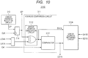
FIG. 10 is a block diagram illustrating a configuration example of the address fault detection circuit inFIG. 9 . - As above, the bus master such as the CPU using the lockstep configuration can detect faults on the bus master. However, the lockstep configuration cannot detect faults outside the lockstep. That is, it is impossible to detect faults on a path between the bus master based on the lockstep configuration and a shared resource, faults in a logic circuit, and faults in the shared resource when the bus master accesses the shared resource such as the memory.
- Concerning the memory, the BIST circuit can detect faults in the memory. However, the technique of the BIST circuit reads a test pattern into the memory using a path inoperable simultaneously with user operations and compares an expected pattern value with a read result. The circuit configuration therefore disables uninterrupted runtime monitoring. Operating the BIST circuit during the runtime allows the BIST circuit to rewrite the data in the memory. The bus master therefore needs to save the memory data in another memory before operating the BIST circuit.
- During the runtime, it may be impossible to detect a fault in the shared resource such as the memory subsequent to a lockstep-based duplexing comparison circuit.
- To solve this, the semiconductor device according to an embodiment includes a comparison circuit that compares a signal accessing the shared resource with an access signal output from the shared resource. It is thereby possible to detect an access signal fault. There is also provided a circuit to hold a faulty access signal. This can isolate a cause of the fault. Supplying the faulty access signal to a comparator can detect a fault of the comparator.
- The description below explains a working example and modifications with reference to the accompanying drawings. In the description below, the same constituent elements are designated by the same reference numerals and a repetitive explanation may be omitted for simplicity.
-
FIGS. 1 through 3 are used to outline a configuration and operation of a microcontroller.FIG. 1 is a block diagram illustrating a configuration example of the microcontroller.FIG. 2 is a block diagram illustrating a flow of addresses and data at the CPU side inFIG. 1 .FIG. 3 is a block diagram illustrating a flow of addresses and data at the memory controller side inFIG. 1 . - A microcontroller 1 is a semiconductor device that includes, in a single semiconductor chip, a
CPU 10 including a master-side CPU 11 and a checker-side CPU 12,local memory 20, afault detection circuit 30, amemory controller 40 including a master-side memory controller 41 and a checker-side memory controller 42, sharedmemory 50, afault detection circuit 60, a DMA controller (DMAC) 70, and abus 80. Thelocal memory 20 and the sharedmemory 50 are configured as SRAM, for example. TheCPU 10 can access thelocal memory 20 and can access also the sharedmemory 50 via thememory controller 40. The DMAC 70 can access also the sharedmemory 50 via thememory controller 40. - The
fault detection circuit 30 at the CPU side includes a master-side addressfault detection circuit 31, a checker-side addressfault detection circuit 32, aduplexing comparison circuit 33, a master-side ECC circuit 34, and a checker-side ECC circuit 35. - The
fault detection circuit 60 at the memory controller side includes a master-side addressfault detection circuit 61, a checker-side addressfault detection circuit 62, aduplexing comparison circuit 63, a master-side ECC circuit 64, and a checker-side ECC circuit 65. - The
CPU 11 as a memory access circuit may read data from thelocal memory 20. In this case, as illustrated inFIG. 2 , theCPU 11 outputs an address signal (CAA1) for memory access to thelocal memory 20, the addressfault detection circuit 31, and theduplexing comparison circuit 33, and reads a data signal (LD) from thelocal memory 20 via theECC circuit 34. TheCPU 12 outputs an address signal (CAA2) for memory access to the addressfault detection circuit 32 and theduplexing comparison circuit 33 and reads a data signal (LD) via theECC circuit 35. Thelocal memory 20 outputs the input address signal (CAA1) as a memory output address signal (LOA) to the addressfault detection circuits - The
CPU 10 may write data to thelocal memory 20. In this case, as illustrated inFIG. 2 , TheCPU 11 outputs an address signal (CAA1) for memory access to thelocal memory 20, the addressfault detection circuit 31, and theduplexing comparison circuit 33, and outputs a data signal (CD1) to thelocal memory 20 and theduplexing comparison circuit 33 via theECC circuit 34. TheCPU 12 outputs the address signal (CAA2) for memory access to the addressfault detection circuit 32 and theduplexing comparison circuit 33, and outputs a data signal (CD2) to theduplexing comparison circuit 33 via theECC circuit 35. Thelocal memory 20 outputs the input address signal (CAA1) as the memory output address signal (LOA) to the addressfault detection circuits - The
CPU 10 may write data to thebus 80. In this case, as illustrated inFIG. 2 , theCPU 11 outputs a data signal (WD1) to theduplexing comparison circuit 33. TheCPU 12 outputs a data signal (WD2) to theduplexing comparison circuit 33. TheCPU 11 may read a data signal (RD1) from thebus 80. In this case, as illustrated inFIG. 2 , theCPU 12 also reads the data signal (RD1). - The
memory controller 40 as a memory access circuit may read data from the sharedmemory 50. In this case, as illustrated inFIG. 3 , thememory controller 41 outputs an address signal (MAA1) for memory access to the sharedmemory 50, the addressfault detection circuit 61, and theduplexing comparison circuit 63, and reads a data signal (KD) from the sharedmemory 50 via theECC circuit 64. Thememory controller 42 outputs an address signal (MAA2) for memory access to the addressfault detection circuit 62 and theduplexing comparison circuit 63, and reads a data signal (KD) from the sharedmemory 50 via theECC circuit 65. The sharedmemory 50 outputs the input address signal (MAA1) as an address signal (KOA) to the addressfault detection circuits - The
memory controller 40 may write data to the sharedmemory 50. In this case, as illustrated inFIG. 3 , thememory controller 41 outputs an address signal (MAA1) for memory access to the sharedmemory 50, the addressfault detection circuit 61, and theduplexing comparison circuit 63, and outputs a data signal (MD1) to the sharedmemory 50 and theduplexing comparison circuit 63 via theECC circuit 64. Thememory controller 42 outputs an address signal (MAA2) for memory access to the addressfault detection circuit 62 and theduplexing comparison circuit 63, and outputs a data signal (MD2) to the via theECC circuit 65. The sharedmemory 50 outputs the input address signal (MAA1) as an address signal (KOA) to the addressfault detection circuits - The
memory controller 40 may read data to thebus 80. In this case, as illustrated inFIG. 3 , thememory controller 41 outputs a data signal (RD1) to theduplexing comparison circuit 63. Thememory controller 42 outputs a data signal (RD2) to theduplexing comparison circuit 63. TheCPU 11 may write a data signal (WD1) to thememory controller 41. In this case, as illustrated inFIG. 3 , the data signal (WD1) is also written to thememory controller 42. - The address
fault detection circuit 31 and theECC circuit 34 detect a fault of thelocal memory 20 in region X1. The addressfault detection circuit 31 detects a fault of an address line or a buffer circuit in region X2 where the address signal (CAA1) is transmitted. The addressfault detection circuit 31 and theduplexing comparison circuit 33 detect a fault of an address line or a buffer circuit in region X3 where the address signal (CAA1) is transmitted. Theduplexing comparison circuit 33 detects a fault of an address line or a buffer circuit in region X4 where the address signal (CAA1) is transmitted. -
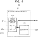
FIGS. 4 through 6 are then used to describe configurations of the fault detection circuits.FIG. 4 is a block diagram illustrating a more detailed configuration of the CPU, the fault detection circuit, and the local memory inFIG. 2 .FIG. 5 is a block diagram illustrating a configuration example of one address fault detection circuit inFIG. 4 .FIG. 6 is a block diagram illustrating a configuration example of another address fault detection circuit inFIG. 4 . - The
CPU 11 includes anaddress generation circuit 13 and anaddress decoder 14 that generates an address signal (CAA1) for memory access and a memory selection signal (MS1) from an original address generated by theaddress generation circuit 13. Theaddress decoder 14 decodes a high-order address of the original address (OA) to generate the memory selection signal (MS1) and outputs a low-order address of the original address (OA) as the address signal (CAA1) for memory access. - The address signal (CAA1) is transmitted to the
duplexing comparison circuit 33, a selection circuit 37, and asynchronization circuit 38 through asignal line 111. The address signal (CAA1) is synchronized with a clock at thesynchronization circuit 38 and is transmitted to the addressfault detection circuit 31. The selection circuit 37 selects the address signal (CAA1) or a test address (TA) for memory BIST. The selected address is transmitted to thelocal memory 20 through asignal line 113. The memory selection signal (MS1) is transmitted to thelocal memory 20 and theduplexing comparison circuit 33 through asignal line 112. - The
CPU 12 is configured similarly to theCPU 11. The address signal (CAA2) for memory access is transmitted to theduplexing comparison circuit 33 and asynchronization circuit 39 through asignal line 121. The address signal (CAA2) is synchronized with a clock at thesynchronization circuit 39 and is transmitted to the addressfault detection circuit 32. The memory selection signal (MS2) is transmitted to theduplexing comparison circuit 33 through a signal line 122. Theduplexing comparison circuit 33 transmits an error signal (DE) to theerror control circuit 36 when a signal from the side of theCPU 11 differs from a signal from the side of theCPU 12. - The
local memory 20 includes asynchronization circuit 23 and asynchronization circuit 24. Thesynchronization circuit 23 synchronizes the address signal (CAA1) for memory access with the clock. Thesynchronization circuit 24 synchronizes the memory selection signal (MS1) with the clock. Thelocal memory 20 further includes anaddress decoder 25, acontrol circuit 26, aword line driver 27, anIO 28, and amemory cell array 29. Theaddress decoder 25 decodes an address signal synchronized at thesynchronization circuit 23. Thecontrol circuit 26 is supplied with a memory selection signal synchronized at thesynchronization circuit 24. Theword line driver 27 is supplied with a row address. TheIO 28 inputs or outputs data from a column selected by a column address. Thelocal memory 20 moreover includes apath 211 that outputs an address signal for memory access synchronized at thesynchronization circuit 23 as a memory output address signal (LOA). The memory output address signal (LOA) from thepath 211 is transmitted to the addressfault detection circuits signal line 212. - As illustrated in
FIG. 5 , the addressfault detection circuit 31 includes anaddress comparison circuit 311, an erroraddress retaining circuit 312, an erroraddress injection circuit 313, and asynchronization circuit 314. Theaddress comparison circuit 311 includes acomparator 3111 and an erroraddress generation circuit 3112. Thecomparator 3111 compares the address signal (CAA1) input to thelocal memory 20 with the memory output address signal (LOA) output from thelocal memory 20 and outputs an error detection signal (ED1) if the compared address signals mismatch. The erroraddress generation circuit 3112 outputs the memory output address signal as an error address signal (EA1). The error detection signal (ED1) is transmitted to theerror control circuit 36. - The error
address retaining circuit 312 uses the error detection signal (ED1) to retain the error address signal (EA1). The erroraddress retaining circuit 312 retains only the first generated error address signal. This is because an address fault requires prompt transition to the safe state. For example, theCPU 11 can read the error address signal (EA1) retained by the erroraddress retaining circuit 312. - The error
address injection circuit 313 injects a predetermined pattern into the erroraddress generation circuit 3112. The erroraddress generation circuit 3112 generates a quasi-error address based on the injected pattern by using a circuit (EOR circuit) that inverts one or more bits in a memory output address (LOA). This can test thecomparator 3111. The erroraddress injection circuit 313 injects a predetermined pattern also into the erroraddress generation circuit 3112 of theaddress comparison circuit 311 of the addressfault detection circuit 32 to be described later. - As illustrated in
FIG. 6 , the addressfault detection circuit 32 includes theaddress comparison circuit 311 but does not include the erroraddress retaining circuit 312, the erroraddress injection circuit 313, and thesynchronization circuit 314. - The
error control circuit 36 detects the error detection signal (ED1 or DE) and outputs an interrupt request signal (IR), a reset request signal (RR), or a terminal output signal (TO) based on settings. The bus master such as the CPU or the system can thereby detect an error occurrence. - The description below explains operations of the entire circuit in
FIG. 4 . - The original address signal (OA) generated from the
address generation circuit 13 in the master-side CPU 11 is input to theaddress decoder 14 and is decoded into the memory selection signal (MS1) and the address signal (CAA1) for memory access. Before input to thelocal memory 20, the memory selection signal (MS1) and the address signal (CAA1) are input to theduplexing comparison circuit 33 and are compared to the memory selection signal (MS2) and the address signal (CAA2) from the checker-side CPU 12, respectively. - The address signal (CAA1) branches to an input to the
duplexing comparison circuit 33 and then passes through a selection circuit (multiplexer) 37 to select a test address signal (TA) for memory BIST. During the runtime (user mode), the selection circuit (multiplexer) 37 always selects the address signal (CAA1) output from the bus master. - The address signal along the
signal line 113 is subject to retiming in thesynchronization circuit 23 configured by a flip-flop in thelocal memory 20, branches prior to theaddress decoder 25, and is output from thelocal memory 20. At this time, a read/write (R/W) access to thelocal memory 20 is performed as usual while the asserted memory selection signal (MS1) and the address signal allow theaddress decoder 25 to select an address space for thememory cell array 29. The memory output address signal (LOA) is input to the addressfault detection circuit 31. Thecomparator 3111 of the addressfault detection circuit 31 compares the address signal (CAA1) with the memory output address signal (LOA). When thecomparator 3111 detects an address signal mismatch, theaddress comparison circuit 311 outputs the memory output address signal (LOA) as an error address (EA1) and the erroraddress retaining circuit 312 retains the error address (EA1). At this time, theaddress comparison circuit 311 inputs the error detection signal (ED1) to theerror control circuit 36. - The memory output address signal (LOA) is input to the address
fault detection circuit 32. Thecomparator 3111 of the addressfault detection circuit 32 compares the address signal (CAA2) with the memory output address signal (LOA). When thecomparator 3111 detects an address signal mismatch, the addressfault detection circuit 32 outputs the memory output address signal (LOA) as an error address (EA2) and outputs an error detection signal (ED2). - When a user predetermines a process for each error, the
error control circuit 36 outputs the reset request signal (RR), the interrupt request signal (IR), and the terminal output signal (TO). The system detects an error occurrence based on these signals output from theerror control circuit 36. Subsequently accessing theerror control circuit 36 and the erroraddress retaining circuit 312 can specify an error cause and a destination address of incorrect writing or reading. - The error
address injection circuit 313 is used to diagnose a fault for thecomparator 3111 of theaddress comparison circuit 311. Setting the erroraddress injection circuit 313 inverts some bits of the memory output address signal (LOA) and allows thecomparator 3111 to perform comparison with the address signal (CAA1). When thecomparator 3111 is not faulty, there obviously occurs a mismatch between a signal output from the erroraddress generation circuit 3112 and the address signal (CAA1), making it possible to test a fault for thecomparator 3111. - With reference to
FIGS. 4 and5 , there has been described the case where theCPU 10 as the memory access circuit accesses thelocal memory 20. The same applies to a case where theCPU 40 as the memory access circuit accesses the sharedmemory 50. - Comparison between an address input to the memory from the memory access circuit and an address output from the memory makes it possible to detect address faults on the memory subsequent to the lockstep. Retaining an address output from the memory as an error address makes it possible to detect a destination address for incorrect writing and specify data destroyed by incorrect writing.
- Typical modifications will be described below. The following description of the modifications assumes that the same reference symbols as used for the above-mentioned working example are used for the parts including the configuration and the function similar to those explained in the above-mentioned working example. The description of the above-mentioned working example is applicable to the description of those parts as needed within a technologically undeviating scope. Parts of the above-mentioned working example and all or part of the modifications are interchangeably applicable as needed within a technologically undeviating scope.
- With reference to
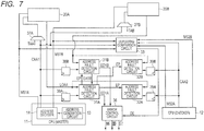
FIGS. 7 and8 , the description below explains a case where there is a plurality of the local memories 20 (for example, two local memories such aslocal memory 20A andlocal memory 20B).FIG. 7 is a block diagram illustrating another configuration example of the CPU, the fault detection circuit, and the local memory inFIG. 2 .FIG. 8 is a block diagram illustrating a configuration example of the address fault detection circuit inFIG. 7 . - The
CPU 11 includes theaddress generation circuit 13 and theaddress decoder 14 that generates an address signal (CAA1) for memory access and memory selection signals (MS1A and MS1B) from an original address generated by theaddress generation circuit 13. Theaddress decoder 14 decodes a high-order address of the original address (OA) to generate the memory selection signals (MS1A and MS1B) and outputs a low-order address of the original address (OA) as the address signal (CAA1) for memory access. - The address signal (CAA1) is transmitted to the
duplexing comparison circuit 33,selection circuits synchronization circuits synchronization circuits fault detection circuits selection circuits local memories local memory 20B and theduplexing comparison circuit 33. The memory selection signal (MS1A) is transmitted to thelocal memory 20A and theduplexing comparison circuit 33. - The
CPU 12 is configured similarly to theCPU 11. The address signal (CAA2) for memory access is transmitted to addressfault detection circuits duplexing comparison circuit 33, andsynchronization circuits duplexing comparison circuit 33. - The
local memories local memory 20. Thelocal memory 20A outputs the address signal for memory access synchronized with the clock at thesynchronization circuit 23 as a memory output address signal (LOAA). Thelocal memory 20B outputs the address signal for memory access synchronized with the clock at thesynchronization circuit 23 as a memory output address signal (LOAB). The memory output address signal (LOAA) is transmitted to the addressfault detection circuits fault detection circuits - As illustrated in
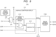
FIG. 8 , the addressfault detection circuit 31A includes theaddress comparison circuit 311, an erroraddress retaining circuit 312A, the erroraddress injection circuit 313, and thesynchronization circuit 314. Theaddress comparison circuit 311 includes thecomparator 3111 and the erroraddress generation circuit 3112. Thecomparator 3111 compares the address signal (CAA1) input to thelocal memory 20 with the memory output address signal (LOAA) output from thelocal memory 20A and outputs an error detection signal (ED1A) if the compared address signals mismatch. The erroraddress generation circuit 3112 outputs the memory output address signal as an error address signal (EA1A). The error detection signal (ED1A) is transmitted to theerror control circuit 36. - The error
address retaining circuit 312A uses the error detection signal (ED1A) to retain the error address signal (EA1A) and uses the error detection signal (ED1B) to retain the error address signal (EA1B). The erroraddress retaining circuit 312A retains only the first generated error address signal. This is because an address fault requires prompt transition to the safe state. For example, theCPU 11 can read the error address signal (EA1A) or the error address signal (EA1B) retained by the erroraddress retaining circuit 312. - The error
address injection circuit 313 injects a predetermined pattern into the erroraddress generation circuit 3112. The erroraddress generation circuit 3112 generates a quasi-error address based on the injected pattern by using the circuit (EOR circuit) that inverts one or more bits in a memory output address (LOAA). This can test thecomparator 3111. The erroraddress injection circuit 313 injects a predetermined pattern also into the erroraddress generation circuit 3112 of theaddress comparison circuit 311 of the addressfault detection circuit 32 to be described later. - Similarly to the address
fault detection circuit 32 according to the working example (FIG. 6 ), the addressfault detection circuits address comparison circuit 311 but do not include the erroraddress retaining circuit 312, the erroraddress injection circuit 313, and thesynchronization circuit 314. The error detection signal (ED1B) and the error address signal (EA1B) are transmitted to the erroraddress retaining circuit 312A of the addressfault detection circuit 31A. - The error detection signal (ED1B) is transmitted to the
error control circuit 36. - The
error control circuit 36 detects the error detection signal (ED1A, ED1B, or DE) and outputs the interrupt request signal (IR), the reset request signal (RR), or the terminal output signal (TO) based on settings. The bus master such as the CPU or the system can thereby detect an error occurrence. - The address signal (CAA2) for memory access is transmitted to the
duplexing comparison circuit 33 and thesynchronization circuits synchronization circuits fault detection circuits duplexing comparison circuit 33. Theduplexing comparison circuit 33 transmits the error signal (DE) to theerror control circuit 36 when a signal from the side of theCPU 11 differs from a signal from the side of theCPU 12. - The
address decoder 14 in theCPU 11 decodes an original address (OA) generated by theaddress generation circuit 13 and generates the memory selection signals (MS1A and MS1B) and an access address (CAA1) for thelocal memories local memory local memory 20A or thelocal memory 20B. Thecomparator 3111 of the addressfault detection circuit CPU 11 with the access address (CAA1) input to thelocal memory CPU 11. When a comparison result from thecomparator 3111 shows a mismatch, the erroraddress retaining circuit 312 retains the error address (EA1A or EA1B) and theerror control circuit 36 is notified of the error detection signal (ED1A or ED1B) similarly to the working example. - Setting the error
address injection circuit 313 can inject a fault into both of the memory output addresses (LOAA and LOAB). The error address injection circuit injects a fault depending on the memory as an access destination to test thecomparator 3111 of the addressfault detection circuit - With reference to
FIGS. 7 and8 , there has been described the case where theCPU 10 as the memory access circuit accesses thelocal memory 20. The same applies to a case where theCPU 40 as the memory access circuit accesses the sharedmemory 50. - It is possible to prevent an area from increasing by allowing each memory to share the duplexing comparison circuit, the error address injection circuit, the error address retaining circuit, or the error control circuit. No need to settle a common circuit for each memory contributes to reducing the software processing time. Moreover, the error address injection circuit can be assigned to address signals output from the memory in common. The test can be performed along the memory space without understanding a physical memory configuration.
- With reference to
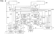
FIGS. 9 and10 , the description below explains an example of performing fault detection on a circuit in the memory access circuit.FIG. 9 is a block diagram illustrating another configuration example of the CPU, the fault detection circuit, and the local memory inFIG. 2 .FIG. 10 is a block diagram illustrating a configuration example of the address fault detection circuit inFIG. 9 . - The
CPU 11 includes theaddress generation circuit 13, theaddress decoder 14, asynchronization circuit 15, and anaddress generation circuit 16. Theaddress decoder 14 generates an address signal (CAA1) for memory access and memory selection signals (MS1A and MS1B) from an original address generated by theaddress generation circuit 13. Theaddress decoder 14 decodes a high-order address of the original address (OA) to generate the memory selection signals (MS1A and MS1B) and outputs a low-order address of the original address (OA1) as the address signal (CAA1) for memory access. Thesynchronization circuit 15 outputs the original address (OA1) synchronized with the clock. The original address (OA1) is transmitted to address fault detection circuits 31AS and 31BS. Theaddress generation circuit 16 generates address signals (UA1A and UA1B) corresponding to the high-order side of the original address (OA) from the memory selection signals (MS1A and MS1B). The address signal (UA1A) is synchronized with the clock at thesynchronization circuit 38A and is transmitted to the address fault detection circuit 31AS. The address signal (UA1B) is synchronized with the clock at thesynchronization circuit 38B and is transmitted to the address fault detection circuit 31BS. - The address signal (CAA1) is transmitted to the
duplexing comparison circuit 33and the
selection circuits selection circuits local memories local memory 20B and theduplexing comparison circuit 33. The memory selection signal (MS1A) is transmitted to thelocal memory 20A and theduplexing comparison circuit 33. - The
CPU 12 is configured similarly to theCPU 11. The address signal (CAA2) for memory access is transmitted to theduplexing comparison circuit 33. The memory selection signals (MS2A and MS2B) are transmitted to theduplexing comparison circuit 33. - The
local memories local memory 20. Thelocal memory 20A outputs the address signal for memory access synchronized at thesynchronization circuit 23 as the memory output address signal (LOAA). Thelocal memory 20B outputs the address signal for memory access synchronized at thesynchronization circuit 23 as the memory output address signal (LOAB). The memory output address signal (LOAA) is transmitted to the address fault detection circuits 31AS and 32AS. The memory output address signal (LOAB) is transmitted to the address fault detection circuits 31BS and 32BS. - As illustrated in
FIG. 10 , the address fault detection circuit 31AS includes theaddress comparison circuit 311, the erroraddress retaining circuit 312A, the erroraddress injection circuit 313, thesynchronization circuit 314, and a coupling circuit 315. Theaddress comparison circuit 311 includes thecomparator 3111 and the erroraddress generation circuit 3112. Thecomparator 3111 compares the original address signal (OA1) input to thelocal memory 20 with an address resulting from coupling the memory output address signal (LOAA) with the high-order address signal (UA1A). The error detection signal (ED1A) is output if the compared address signals mismatch. The erroraddress generation circuit 3112 outputs a memory output address signal as the error address signal (EA1A). The error detection signal (ED1A) is transmitted to theerror control circuit 36. - The error
address retaining circuit 312A equals the first modification. The erroraddress injection circuit 313 equals the first modification. - The address fault detection circuits 31BS, 32AS, and 32BS include the
address comparison circuit 311 and the coupling circuit 315 but do not include the erroraddress retaining circuit 312A, the erroraddress injection circuit 313, and thesynchronization circuit 314. The error detection signal (ED1B) or the error address signal (EA1B) is transmitted to the erroraddress retaining circuit 312 of the addressfault detection circuit 31A. The erroraddress retaining circuit 312 retains only the first generated error address signal. This is because an address fault requires prompt transition to the safe state. For example, theCPU 11 can read the error address signal (EA1A) or the error address signal (EA1B) retained by the erroraddress retaining circuit 312. - The error detection signal (ED1B) is transmitted to the
error control circuit 36. - The
error control circuit 36 detects the error detection signal (ED1A, ED1B, or DE) and outputs the interrupt request signal (IR), the reset request signal (RR), or the terminal output signal (TO) based on settings. The bus master such as the CPU or the system can thereby detect an error occurrence. - The
CPU 12 is configured similarly to theCPU 11. Theaddress generation circuit 16 generates address signals (UA2A and UA2B) corresponding to the high-order side of the original address (OA) from the memory selection signals (MS2A and MS2B). The address signal (UA2A) is synchronized with the clock at thesynchronization circuit 39A and is transmitted to the addressfault detection circuit 32A. The address signal (UA2B) is synchronized with the clock at thesynchronization circuit 39B and is transmitted to the addressfault detection circuit 32B. The address signal (CAA2) for memory access is transmitted to theduplexing comparison circuit 33. The memory selection signals (MS2A and MS2B) are transmitted to theduplexing comparison circuit 33. Theduplexing comparison circuit 33 transmits the error signal (DE) to theerror control circuit 36 when a signal from the side of theCPU 11 differs from a signal from the side of theCPU 12. - The
address generation circuit 16 in theCPU 11 encodes the memory selection signal (MS1A or MS1B) output from theaddress decoder 14 to again generate a high-order address signal (UA1A or US1B). Thecomparator 3111 of the addressfault detection circuit address generation circuit 13 with an address signal resulting from coupling the high-order address signal (UA1A or US1B) generated by theaddress generation circuit 16 with the low-order address signal (memory output signal LOAA or LOAB)) output from thelocal memory address decoder 14. - With reference to
FIGS. 9 and10 , there has been described the case where theCPU 10 as the memory access circuit accesses thelocal memory 20. The same applies to a case where theCPU 40 as the memory access circuit accesses the sharedmemory 50. - According to the working example and the first modification, the address fault detection circuit cannot detect a fault on the address line or the address decoder in the memory access circuit. According to the second modification, an address before input to the address decoder in the memory access circuit is output outside the bus master and is compared with an address output from the memory in the address fault detection circuit. It is thereby possible to detect a fault on the address decoder in the memory access circuit of a product that includes the memory access circuit unrelated to the lockstep configuration.
- While there has been described the embodiment, the working example, and the modifications of the present invention created by the inventors, it is to be distinctly understood that the present invention is not limited to the embodiment, the working example, and the modifications, but may be otherwise variously modified.
- For example, the working example and the modifications have described the case where the memory access circuit accesses the memory, but not limited thereto. The above is also applicable to a case where the memory access circuit accesses the shared resource such as a circuit including a register.
- The working example and the modifications have described detection of a fault on an address path by comparing addresses to access the memory, but not limited thereto. For example, memory selection signals may be compared.
- The working example and the modifications have described the case of using one set of the master-side CPU and the checker-side CPU and one set of the local memory and the fault detection circuit, but not limited thereto. Two or more sets may be applicable.
Claims (17)
- A semiconductor device comprising:a first memory access circuit;a second memory access circuit to check the first memory access circuit;a memory that outputs a memory address based on a first access address input from the first memory access circuit;a duplexing comparison circuit that compares the first access address with a second access address output from the second memory access circuit;a first address comparison circuit that compares the first access address with the memory address; andan error control circuit that outputs a control signal based on a comparison result from the duplexing comparison circuit and a comparison result from the first address comparison circuit.
- The semiconductor device according to claim 1, wherein the first address comparison circuit includes:an error injection circuit that generates a pattern to generate an error address;a first error address generation circuit that generates a first error address based on the memory address and an output from the error injection circuit;a first comparison circuit that compares the first access address with a first address output from the first error address generation circuit; andan error address retaining circuit that retains the first address based on a comparison result from the first comparison circuit,wherein the first address corresponds to one of the first error address and the second access address.
- The semiconductor device according to claim 2, further comprising:a second address comparison circuit that compares the second access address with the memory address,wherein the second address comparison circuit includes:a second error address generation circuit that generates a second error address based on the memory address and an output from the error injection circuit; anda second comparison circuit that compares the second access address with a second address output from the second error address generation circuit; andwherein the second address corresponds to one of the second error address and the first access address.
- The semiconductor device according to claim 1, wherein the first memory access circuit and the second memory access circuit each correspond to a CPU.
- The semiconductor device according to claim 1, wherein the first memory access circuit and the second memory access circuit each correspond to a memory controller.
- A semiconductor device comprising:a first memory access circuit;a first memory that outputs a first memory address based on a first access address input from the first memory access circuit;a second memory that outputs a second memory address based on a first access address input from the first memory access circuit;a first address comparison circuit that compares the first access address with the first memory address;a second address comparison circuit that compares the first access address with the second memory address; andan error control circuit that outputs a control signal based on a comparison result from the first address comparison circuit and a comparison result from the second comparison circuit.
- The semiconductor device according to claim 6, wherein the first address comparison circuit includes:an error injection circuit that generates a pattern to generate an error address;a first error address generation circuit that generates a first error address based on the first memory address and an output from the error injection circuit;a first comparison circuit that compares the first access address with a first address output from the first error address generation circuit; andan error address retaining circuit that retains the first address based on a comparison result from the first comparison circuit;wherein the second address comparison circuit includes:a second error address generation circuit that generates a second error address based on the second memory address and an output from the error injection circuit; anda second comparison circuit that compares the first access address with a second address output from the second error address generation circuit;wherein the first address corresponds to one of the first error address and the first access address;wherein the second address corresponds to one of the second error address and the first access address; andwherein the error address retaining circuit retains the second address based on a comparison result from the second comparison circuit.
- The semiconductor device according to claim 7, further comprising:a second memory access circuit to check the first memory access circuit; anda duplexing comparison circuit that compares a first access address output from the first memory access circuit with a second access address output from the second memory access circuit, compares a first memory selection signal output from the first memory access circuit with a third memory selection signal output from the second memory access circuit, and compares a second memory selection signal output from the first memory access circuit with a fourth memory selection signal output from the second memory access circuit; andwherein the error control circuit outputs a control signal based on a comparison result from the duplexing comparison circuit.
- The semiconductor device according to claim 8, further comprising:a third address comparison circuit that compares the second access address and the first memory address; anda fourth address comparison circuit that compares the second access address and the second memory address,wherein a third address comparison circuit includes:a third error address generation circuit that generates a third error address based on the first memory address an output from the error injection circuit; anda third comparison circuit that compares the second access address with a third address output from the third error address generation circuit,wherein a fourth address comparison circuit includes:a fourth error address generation circuit that generates a fourth error address based on the second memory address and an output from the error injection circuit;a fourth comparison circuit that compares the second access address with a fourth address output from the fourth error address generation circuit;wherein the third address corresponds to one of the third error address and the second access address; andwherein the fourth address corresponds to one of the fourth error address and the second access address.
- The semiconductor device according to claim 6, wherein the first memory access circuit and the second memory access circuit correspond to a CPU.
- The semiconductor device according to claim 6, wherein the first memory access circuit and the second memory access circuit correspond to a memory controller.
- A semiconductor device comprising:a first memory access circuit including a first address generation circuit, a first address decoder to generate a first access address, a first memory selection signal, and a second memory selection signal from a first original address generated by the first address generation circuit, and a second address generation circuit to generate a high-order address of the first access address from the first memory selection signal and the second memory selection signal;a first memory that generates a first memory address based on the first access address;a second memory that generates a second memory address based on the first access address;a first address comparison circuit that compares the first original address with a first restoration address resulting from combining the first memory address with a high-order address of the first access address;a second address comparison circuit that compares the first original address with a second restoration address resulting from combining the second memory address with a high-order address of the first access address; andan error control circuit that outputs a control signal based on one of a comparison result from the first address comparison circuit and a comparison result from the second address comparison circuit.
- The semiconductor device according to claim 12, wherein the first address comparison circuit includes:an error injection circuit that generates a pattern to generate an error address;a first error address generation circuit that generates a first error address based on the first memory address and an output from the error injection circuit;a first comparison circuit that compares the first restoration address with a first address output from the first error address generation circuit; andan error address retaining circuit that retains the first address based on a comparison result from the first comparison circuit;wherein the second address comparison circuit includes:a second error address generation circuit that generates a second error address based on the second memory address and an output from the error injection circuit; anda second comparison circuit that compares the second restoration address with a second address output from the second error address generation circuit;wherein the first address corresponds to one of the first error address and the first access address;wherein the second address corresponds to one of the second error address and the first access address; andwherein the error address retaining circuit retains the second address based on a comparison result from the second comparison circuit.
- The semiconductor device according to claim 13, further comprising:a second memory access circuit including a third address generation circuit, a second address decoder to generate a second access address, a third memory selection signal, and a fourth memory selection signal from a second original address generated by the third address generation circuit, and a fourth address generation circuit to generate a high-order address of the second access address from the third memory selection signal and the fourth memory selection signal; anda duplexing comparison circuit that compares a first access address with a second access address, compares a first memory selection signal with a third selection signal, and compares a second memory selection signal with a fourth selection signal,wherein the error control circuit outputs a control signal based on a comparison result from the duplexing comparison circuit.
- The semiconductor device according to claim 14, further comprising:a third address comparison circuit that compares the second original address with a third restoration address resulting from combining the first memory address with a high-order address of the second access address; anda fourth address comparison circuit that compares the second original address with a fourth restoration address resulting from combining the second memory address with a high-order address of the second access address,wherein the third address comparison circuit includes:a third error address generation circuit that generates a third error address based on the first memory address and an output from the error injection circuit;a third comparison circuit that compares the third restoration address with a third address output from the third error address generation circuit;wherein the fourth address comparison circuit includes:a fourth error address generation circuit that generates a fourth error address based on the second memory address and an output from the error injection circuit; anda fourth comparison circuit that compares the fourth restoration address with a fourth address output from the fourth error address generation circuit;wherein the third address corresponds to one of the third error address and the second access address; andwherein the fourth address corresponds to one of the fourth error address and the second access address.
- The semiconductor device according to claim 12, wherein the first memory access circuit and the second memory access circuit correspond to a CPU.
- The semiconductor device according to claim 12, wherein the first memory access circuit and the second memory access circuit correspond to a memory controller.
Applications Claiming Priority (1)
| Application Number | Priority Date | Filing Date | Title |
|---|---|---|---|
| JP2017189496A JP2019066983A (en) | 2017-09-29 | 2017-09-29 | Semiconductor device |
Publications (3)
| Publication Number | Publication Date |
|---|---|
| EP3508979A2 true EP3508979A2 (en) | 2019-07-10 |
| EP3508979A3 EP3508979A3 (en) | 2019-07-24 |
| EP3508979B1 EP3508979B1 (en) | 2022-11-09 |
Family
ID=63449184
Family Applications (1)
| Application Number | Title | Priority Date | Filing Date |
|---|---|---|---|
| EP18188636.7A Active EP3508979B1 (en) | 2017-09-29 | 2018-08-13 | Semiconductor device |
Country Status (5)
| Country | Link |
|---|---|
| US (1) | US10725880B2 (en) |
| EP (1) | EP3508979B1 (en) |
| JP (1) | JP2019066983A (en) |
| KR (1) | KR20190038345A (en) |
| CN (1) | CN109614277B (en) |
Families Citing this family (5)
| Publication number | Priority date | Publication date | Assignee | Title |
|---|---|---|---|---|
| US10922203B1 (en) * | 2018-09-21 | 2021-02-16 | Nvidia Corporation | Fault injection architecture for resilient GPU computing |
| US11221899B2 (en) * | 2019-09-24 | 2022-01-11 | Arm Limited | Efficient memory utilisation in a processing cluster having a split mode and a lock mode |
| KR102826233B1 (en) * | 2020-06-02 | 2025-06-26 | 삼성전자주식회사 | Memory module and method for operating memory module |
| US11392455B1 (en) * | 2021-02-26 | 2022-07-19 | Texas Instruments Incorporated | Methods, apparatus, and articles of manufacture to determine memory access integrity based on feedback from memory |
| US12135624B2 (en) * | 2022-12-14 | 2024-11-05 | Renesas Electronics Corporation | Circuits, systems, and methods for ECC fault detection |
Citations (1)
| Publication number | Priority date | Publication date | Assignee | Title |
|---|---|---|---|---|
| US20130038945A1 (en) | 2011-08-08 | 2013-02-14 | Canon Kabushiki Kaisha | Wide-angle converter lens |
Family Cites Families (6)
| Publication number | Priority date | Publication date | Assignee | Title |
|---|---|---|---|---|
| JPH0314033A (en) | 1989-06-12 | 1991-01-22 | Fujitsu Ltd | Inspection system for microprocessor comparison checking function |
| US5231640A (en) | 1990-07-20 | 1993-07-27 | Unisys Corporation | Fault tolerant processor/memory architecture |
| FR2803057B1 (en) * | 1999-12-22 | 2002-11-29 | Centre Nat Etd Spatiales | COMPUTER SYSTEM TOLERANT TO TRANSIENT ERRORS AND MANAGEMENT METHOD IN SUCH A SYSTEM |
| JP2015035121A (en) * | 2013-08-09 | 2015-02-19 | ルネサスエレクトロニクス株式会社 | Semiconductor integrated circuit device |
| JP6605359B2 (en) * | 2016-03-02 | 2019-11-13 | ルネサスエレクトロニクス株式会社 | Semiconductor device and memory access control method |
| US10204698B2 (en) * | 2016-12-20 | 2019-02-12 | Ampere Computing Llc | Method to dynamically inject errors in a repairable memory on silicon and a method to validate built-in-self-repair logic |
-
2017
- 2017-09-29 JP JP2017189496A patent/JP2019066983A/en active Pending
-
2018
- 2018-08-09 US US16/059,903 patent/US10725880B2/en active Active
- 2018-08-13 EP EP18188636.7A patent/EP3508979B1/en active Active
- 2018-09-19 KR KR1020180112180A patent/KR20190038345A/en not_active Withdrawn
- 2018-09-21 CN CN201811106841.5A patent/CN109614277B/en active Active
Patent Citations (1)
| Publication number | Priority date | Publication date | Assignee | Title |
|---|---|---|---|---|
| US20130038945A1 (en) | 2011-08-08 | 2013-02-14 | Canon Kabushiki Kaisha | Wide-angle converter lens |
Also Published As
| Publication number | Publication date |
|---|---|
| EP3508979B1 (en) | 2022-11-09 |
| CN109614277B (en) | 2023-04-28 |
| KR20190038345A (en) | 2019-04-08 |
| US10725880B2 (en) | 2020-07-28 |
| US20190102271A1 (en) | 2019-04-04 |
| EP3508979A3 (en) | 2019-07-24 |
| JP2019066983A (en) | 2019-04-25 |
| CN109614277A (en) | 2019-04-12 |
Similar Documents
| Publication | Publication Date | Title |
|---|---|---|
| EP3508979B1 (en) | Semiconductor device | |
| US9904596B2 (en) | Serial bus event notification in a memory device | |
| US9880901B2 (en) | Serial bus DRAM error correction event notification | |
| KR102553704B1 (en) | Dynamic application of ECC based on error type | |
| US7206891B2 (en) | Multi-port memory controller having independent ECC encoders | |
| US9959164B2 (en) | Semiconductor device and driving method thereof | |
| US7299400B2 (en) | Error correction circuit | |
| US9396079B2 (en) | Semiconductor memory device and semiconductor system including the same | |
| US9104588B2 (en) | Circuits, apparatuses, and methods for address scrambling | |
| US8767502B2 (en) | Semiconductor device verifying signal supplied from outside | |
| KR20160115752A (en) | Diagnostic program, diagnostic method, and semiconductor device | |
| JP2015118468A (en) | Programmable controller | |
| TWI655637B (en) | Memory device | |
| US20170287571A1 (en) | Buffer circuit with adaptive repair capability | |
| US8995217B2 (en) | Hybrid latch and fuse scheme for memory repair | |
| US20050219886A1 (en) | Memory device with built-in test function and method for controlling the same | |
| US9779834B2 (en) | Memory system for improving programming operation on fuse array | |
| US7464309B2 (en) | Method and apparatus for testing semiconductor memory device and related testing methods | |
| JP2017010273A (en) | Semiconductor failure detection device | |
| KR20020095028A (en) | Test method and test system for semiconductor device | |
| JP2007066423A (en) | Semiconductor integrated circuit device | |
| EP3751572A1 (en) | Memory device | |
| US8289792B2 (en) | Memory test circuit, semiconductor integrated circuit and memory test method | |
| CN101494083B (en) | Random access memory and method for resetting its execution data | |
| US11315656B1 (en) | Detection circuit and detection method |
Legal Events
| Date | Code | Title | Description |
|---|---|---|---|
| PUAI | Public reference made under article 153(3) epc to a published international application that has entered the european phase |
Free format text: ORIGINAL CODE: 0009012 |
|
| STAA | Information on the status of an ep patent application or granted ep patent |
Free format text: STATUS: THE APPLICATION HAS BEEN PUBLISHED |
|
| PUAL | Search report despatched |
Free format text: ORIGINAL CODE: 0009013 |
|
| AK | Designated contracting states |
Kind code of ref document: A2 Designated state(s): AL AT BE BG CH CY CZ DE DK EE ES FI FR GB GR HR HU IE IS IT LI LT LU LV MC MK MT NL NO PL PT RO RS SE SI SK SM TR |
|
| AX | Request for extension of the european patent |
Extension state: BA ME |
|
| AK | Designated contracting states |
Kind code of ref document: A3 Designated state(s): AL AT BE BG CH CY CZ DE DK EE ES FI FR GB GR HR HU IE IS IT LI LT LU LV MC MK MT NL NO PL PT RO RS SE SI SK SM TR |
|
| AX | Request for extension of the european patent |
Extension state: BA ME |
|
| RIC1 | Information provided on ipc code assigned before grant |
Ipc: G06F 11/16 20060101AFI20190618BHEP Ipc: G06F 11/10 20060101ALN20190618BHEP Ipc: G06F 11/22 20060101ALN20190618BHEP |
|
| STAA | Information on the status of an ep patent application or granted ep patent |
Free format text: STATUS: REQUEST FOR EXAMINATION WAS MADE |
|
| 17P | Request for examination filed |
Effective date: 20200124 |
|
| RBV | Designated contracting states (corrected) |
Designated state(s): AL AT BE BG CH CY CZ DE DK EE ES FI FR GB GR HR HU IE IS IT LI LT LU LV MC MK MT NL NO PL PT RO RS SE SI SK SM TR |
|
| STAA | Information on the status of an ep patent application or granted ep patent |
Free format text: STATUS: EXAMINATION IS IN PROGRESS |
|
| 17Q | First examination report despatched |
Effective date: 20201109 |
|
| GRAP | Despatch of communication of intention to grant a patent |
Free format text: ORIGINAL CODE: EPIDOSNIGR1 |
|
| STAA | Information on the status of an ep patent application or granted ep patent |
Free format text: STATUS: GRANT OF PATENT IS INTENDED |
|
| RIC1 | Information provided on ipc code assigned before grant |
Ipc: G06F 11/22 20060101ALN20220628BHEP Ipc: G06F 11/10 20060101ALN20220628BHEP Ipc: G06F 11/27 20060101ALI20220628BHEP Ipc: G06F 11/16 20060101AFI20220628BHEP |
|
| INTG | Intention to grant announced |
Effective date: 20220712 |
|
| GRAS | Grant fee paid |
Free format text: ORIGINAL CODE: EPIDOSNIGR3 |
|
| GRAA | (expected) grant |
Free format text: ORIGINAL CODE: 0009210 |
|
| STAA | Information on the status of an ep patent application or granted ep patent |
Free format text: STATUS: THE PATENT HAS BEEN GRANTED |
|
| AK | Designated contracting states |
Kind code of ref document: B1 Designated state(s): AL AT BE BG CH CY CZ DE DK EE ES FI FR GB GR HR HU IE IS IT LI LT LU LV MC MK MT NL NO PL PT RO RS SE SI SK SM TR |
|
| REG | Reference to a national code |
Ref country code: GB Ref legal event code: FG4D |
|
| REG | Reference to a national code |
Ref country code: CH Ref legal event code: EP Ref country code: AT Ref legal event code: REF Ref document number: 1530822 Country of ref document: AT Kind code of ref document: T Effective date: 20221115 |
|
| REG | Reference to a national code |
Ref country code: IE Ref legal event code: FG4D |
|
| REG | Reference to a national code |
Ref country code: DE Ref legal event code: R096 Ref document number: 602018042784 Country of ref document: DE |
|
| REG | Reference to a national code |
Ref country code: LT Ref legal event code: MG9D |
|
| REG | Reference to a national code |
Ref country code: NL Ref legal event code: MP Effective date: 20221109 |
|
| REG | Reference to a national code |
Ref country code: AT Ref legal event code: MK05 Ref document number: 1530822 Country of ref document: AT Kind code of ref document: T Effective date: 20221109 |
|
| PG25 | Lapsed in a contracting state [announced via postgrant information from national office to epo] |
Ref country code: SE Free format text: LAPSE BECAUSE OF FAILURE TO SUBMIT A TRANSLATION OF THE DESCRIPTION OR TO PAY THE FEE WITHIN THE PRESCRIBED TIME-LIMIT Effective date: 20221109 Ref country code: PT Free format text: LAPSE BECAUSE OF FAILURE TO SUBMIT A TRANSLATION OF THE DESCRIPTION OR TO PAY THE FEE WITHIN THE PRESCRIBED TIME-LIMIT Effective date: 20230309 Ref country code: NO Free format text: LAPSE BECAUSE OF FAILURE TO SUBMIT A TRANSLATION OF THE DESCRIPTION OR TO PAY THE FEE WITHIN THE PRESCRIBED TIME-LIMIT Effective date: 20230209 Ref country code: LT Free format text: LAPSE BECAUSE OF FAILURE TO SUBMIT A TRANSLATION OF THE DESCRIPTION OR TO PAY THE FEE WITHIN THE PRESCRIBED TIME-LIMIT Effective date: 20221109 Ref country code: FI Free format text: LAPSE BECAUSE OF FAILURE TO SUBMIT A TRANSLATION OF THE DESCRIPTION OR TO PAY THE FEE WITHIN THE PRESCRIBED TIME-LIMIT Effective date: 20221109 Ref country code: ES Free format text: LAPSE BECAUSE OF FAILURE TO SUBMIT A TRANSLATION OF THE DESCRIPTION OR TO PAY THE FEE WITHIN THE PRESCRIBED TIME-LIMIT Effective date: 20221109 Ref country code: AT Free format text: LAPSE BECAUSE OF FAILURE TO SUBMIT A TRANSLATION OF THE DESCRIPTION OR TO PAY THE FEE WITHIN THE PRESCRIBED TIME-LIMIT Effective date: 20221109 |
|
| PG25 | Lapsed in a contracting state [announced via postgrant information from national office to epo] |
Ref country code: RS Free format text: LAPSE BECAUSE OF FAILURE TO SUBMIT A TRANSLATION OF THE DESCRIPTION OR TO PAY THE FEE WITHIN THE PRESCRIBED TIME-LIMIT Effective date: 20221109 Ref country code: PL Free format text: LAPSE BECAUSE OF FAILURE TO SUBMIT A TRANSLATION OF THE DESCRIPTION OR TO PAY THE FEE WITHIN THE PRESCRIBED TIME-LIMIT Effective date: 20221109 Ref country code: LV Free format text: LAPSE BECAUSE OF FAILURE TO SUBMIT A TRANSLATION OF THE DESCRIPTION OR TO PAY THE FEE WITHIN THE PRESCRIBED TIME-LIMIT Effective date: 20221109 Ref country code: IS Free format text: LAPSE BECAUSE OF FAILURE TO SUBMIT A TRANSLATION OF THE DESCRIPTION OR TO PAY THE FEE WITHIN THE PRESCRIBED TIME-LIMIT Effective date: 20230309 Ref country code: HR Free format text: LAPSE BECAUSE OF FAILURE TO SUBMIT A TRANSLATION OF THE DESCRIPTION OR TO PAY THE FEE WITHIN THE PRESCRIBED TIME-LIMIT Effective date: 20221109 Ref country code: GR Free format text: LAPSE BECAUSE OF FAILURE TO SUBMIT A TRANSLATION OF THE DESCRIPTION OR TO PAY THE FEE WITHIN THE PRESCRIBED TIME-LIMIT Effective date: 20230210 |
|
| PG25 | Lapsed in a contracting state [announced via postgrant information from national office to epo] |
Ref country code: NL Free format text: LAPSE BECAUSE OF FAILURE TO SUBMIT A TRANSLATION OF THE DESCRIPTION OR TO PAY THE FEE WITHIN THE PRESCRIBED TIME-LIMIT Effective date: 20221109 |
|
| PG25 | Lapsed in a contracting state [announced via postgrant information from national office to epo] |
Ref country code: SM Free format text: LAPSE BECAUSE OF FAILURE TO SUBMIT A TRANSLATION OF THE DESCRIPTION OR TO PAY THE FEE WITHIN THE PRESCRIBED TIME-LIMIT Effective date: 20221109 Ref country code: RO Free format text: LAPSE BECAUSE OF FAILURE TO SUBMIT A TRANSLATION OF THE DESCRIPTION OR TO PAY THE FEE WITHIN THE PRESCRIBED TIME-LIMIT Effective date: 20221109 Ref country code: EE Free format text: LAPSE BECAUSE OF FAILURE TO SUBMIT A TRANSLATION OF THE DESCRIPTION OR TO PAY THE FEE WITHIN THE PRESCRIBED TIME-LIMIT Effective date: 20221109 Ref country code: DK Free format text: LAPSE BECAUSE OF FAILURE TO SUBMIT A TRANSLATION OF THE DESCRIPTION OR TO PAY THE FEE WITHIN THE PRESCRIBED TIME-LIMIT Effective date: 20221109 Ref country code: CZ Free format text: LAPSE BECAUSE OF FAILURE TO SUBMIT A TRANSLATION OF THE DESCRIPTION OR TO PAY THE FEE WITHIN THE PRESCRIBED TIME-LIMIT Effective date: 20221109 |
|
| REG | Reference to a national code |
Ref country code: DE Ref legal event code: R097 Ref document number: 602018042784 Country of ref document: DE |
|
| PG25 | Lapsed in a contracting state [announced via postgrant information from national office to epo] |
Ref country code: SK Free format text: LAPSE BECAUSE OF FAILURE TO SUBMIT A TRANSLATION OF THE DESCRIPTION OR TO PAY THE FEE WITHIN THE PRESCRIBED TIME-LIMIT Effective date: 20221109 Ref country code: AL Free format text: LAPSE BECAUSE OF FAILURE TO SUBMIT A TRANSLATION OF THE DESCRIPTION OR TO PAY THE FEE WITHIN THE PRESCRIBED TIME-LIMIT Effective date: 20221109 |
|
| PLBE | No opposition filed within time limit |
Free format text: ORIGINAL CODE: 0009261 |
|
| STAA | Information on the status of an ep patent application or granted ep patent |
Free format text: STATUS: NO OPPOSITION FILED WITHIN TIME LIMIT |
|
| 26N | No opposition filed |
Effective date: 20230810 |
|
| PG25 | Lapsed in a contracting state [announced via postgrant information from national office to epo] |
Ref country code: SI Free format text: LAPSE BECAUSE OF FAILURE TO SUBMIT A TRANSLATION OF THE DESCRIPTION OR TO PAY THE FEE WITHIN THE PRESCRIBED TIME-LIMIT Effective date: 20221109 |
|
| PG25 | Lapsed in a contracting state [announced via postgrant information from national office to epo] |
Ref country code: MC Free format text: LAPSE BECAUSE OF FAILURE TO SUBMIT A TRANSLATION OF THE DESCRIPTION OR TO PAY THE FEE WITHIN THE PRESCRIBED TIME-LIMIT Effective date: 20221109 |
|
| REG | Reference to a national code |
Ref country code: CH Ref legal event code: PL |
|
| PG25 | Lapsed in a contracting state [announced via postgrant information from national office to epo] |
Ref country code: MC Free format text: LAPSE BECAUSE OF FAILURE TO SUBMIT A TRANSLATION OF THE DESCRIPTION OR TO PAY THE FEE WITHIN THE PRESCRIBED TIME-LIMIT Effective date: 20221109 |
|
| PG25 | Lapsed in a contracting state [announced via postgrant information from national office to epo] |
Ref country code: LU Free format text: LAPSE BECAUSE OF NON-PAYMENT OF DUE FEES Effective date: 20230813 |
|
| GBPC | Gb: european patent ceased through non-payment of renewal fee |
Effective date: 20230813 |
|
| PG25 | Lapsed in a contracting state [announced via postgrant information from national office to epo] |
Ref country code: LU Free format text: LAPSE BECAUSE OF NON-PAYMENT OF DUE FEES Effective date: 20230813 Ref country code: CH Free format text: LAPSE BECAUSE OF NON-PAYMENT OF DUE FEES Effective date: 20230831 |
|
| REG | Reference to a national code |
Ref country code: BE Ref legal event code: MM Effective date: 20230831 |
|
| REG | Reference to a national code |
Ref country code: IE Ref legal event code: MM4A |
|
| PG25 | Lapsed in a contracting state [announced via postgrant information from national office to epo] |
Ref country code: IT Free format text: LAPSE BECAUSE OF FAILURE TO SUBMIT A TRANSLATION OF THE DESCRIPTION OR TO PAY THE FEE WITHIN THE PRESCRIBED TIME-LIMIT Effective date: 20221109 |
|
| PG25 | Lapsed in a contracting state [announced via postgrant information from national office to epo] |
Ref country code: IE Free format text: LAPSE BECAUSE OF NON-PAYMENT OF DUE FEES Effective date: 20230813 |
|
| PG25 | Lapsed in a contracting state [announced via postgrant information from national office to epo] |
Ref country code: GB Free format text: LAPSE BECAUSE OF NON-PAYMENT OF DUE FEES Effective date: 20230813 |
|
| PG25 | Lapsed in a contracting state [announced via postgrant information from national office to epo] |
Ref country code: IE Free format text: LAPSE BECAUSE OF NON-PAYMENT OF DUE FEES Effective date: 20230813 Ref country code: GB Free format text: LAPSE BECAUSE OF NON-PAYMENT OF DUE FEES Effective date: 20230813 Ref country code: FR Free format text: LAPSE BECAUSE OF NON-PAYMENT OF DUE FEES Effective date: 20230831 |
|
| PG25 | Lapsed in a contracting state [announced via postgrant information from national office to epo] |
Ref country code: BE Free format text: LAPSE BECAUSE OF NON-PAYMENT OF DUE FEES Effective date: 20230831 |
|
| PG25 | Lapsed in a contracting state [announced via postgrant information from national office to epo] |
Ref country code: BG Free format text: LAPSE BECAUSE OF FAILURE TO SUBMIT A TRANSLATION OF THE DESCRIPTION OR TO PAY THE FEE WITHIN THE PRESCRIBED TIME-LIMIT Effective date: 20221109 |
|
| PG25 | Lapsed in a contracting state [announced via postgrant information from national office to epo] |
Ref country code: BG Free format text: LAPSE BECAUSE OF FAILURE TO SUBMIT A TRANSLATION OF THE DESCRIPTION OR TO PAY THE FEE WITHIN THE PRESCRIBED TIME-LIMIT Effective date: 20221109 |
|
| PG25 | Lapsed in a contracting state [announced via postgrant information from national office to epo] |
Ref country code: CY Free format text: LAPSE BECAUSE OF FAILURE TO SUBMIT A TRANSLATION OF THE DESCRIPTION OR TO PAY THE FEE WITHIN THE PRESCRIBED TIME-LIMIT; INVALID AB INITIO Effective date: 20180813 |
|
| PG25 | Lapsed in a contracting state [announced via postgrant information from national office to epo] |
Ref country code: HU Free format text: LAPSE BECAUSE OF FAILURE TO SUBMIT A TRANSLATION OF THE DESCRIPTION OR TO PAY THE FEE WITHIN THE PRESCRIBED TIME-LIMIT; INVALID AB INITIO Effective date: 20180813 |
|
| PGFP | Annual fee paid to national office [announced via postgrant information from national office to epo] |
Ref country code: DE Payment date: 20250827 Year of fee payment: 8 |
|
| PG25 | Lapsed in a contracting state [announced via postgrant information from national office to epo] |
Ref country code: TR Free format text: LAPSE BECAUSE OF FAILURE TO SUBMIT A TRANSLATION OF THE DESCRIPTION OR TO PAY THE FEE WITHIN THE PRESCRIBED TIME-LIMIT Effective date: 20221109 |