EP3506354A1 - Light emitting device, projector, and method of manufacturing light emitting device - Google Patents
Light emitting device, projector, and method of manufacturing light emitting device Download PDFInfo
- Publication number
- EP3506354A1 EP3506354A1 EP18215349.4A EP18215349A EP3506354A1 EP 3506354 A1 EP3506354 A1 EP 3506354A1 EP 18215349 A EP18215349 A EP 18215349A EP 3506354 A1 EP3506354 A1 EP 3506354A1
- Authority
- EP
- European Patent Office
- Prior art keywords
- light emitting
- base member
- height
- layer
- emitting device
- Prior art date
- Legal status (The legal status is an assumption and is not a legal conclusion. Google has not performed a legal analysis and makes no representation as to the accuracy of the status listed.)
- Granted
Links
Images









Classifications
-
- H—ELECTRICITY
- H10—SEMICONDUCTOR DEVICES; ELECTRIC SOLID-STATE DEVICES NOT OTHERWISE PROVIDED FOR
- H10H—INORGANIC LIGHT-EMITTING SEMICONDUCTOR DEVICES HAVING POTENTIAL BARRIERS
- H10H29/00—Integrated devices, or assemblies of multiple devices, comprising at least one light-emitting semiconductor element covered by group H10H20/00
- H10H29/10—Integrated devices comprising at least one light-emitting semiconductor component covered by group H10H20/00
-
- H—ELECTRICITY
- H10—SEMICONDUCTOR DEVICES; ELECTRIC SOLID-STATE DEVICES NOT OTHERWISE PROVIDED FOR
- H10H—INORGANIC LIGHT-EMITTING SEMICONDUCTOR DEVICES HAVING POTENTIAL BARRIERS
- H10H20/00—Individual inorganic light-emitting semiconductor devices having potential barriers, e.g. light-emitting diodes [LED]
- H10H20/80—Constructional details
- H10H20/85—Packages
-
- G—PHYSICS
- G03—PHOTOGRAPHY; CINEMATOGRAPHY; ANALOGOUS TECHNIQUES USING WAVES OTHER THAN OPTICAL WAVES; ELECTROGRAPHY; HOLOGRAPHY
- G03B—APPARATUS OR ARRANGEMENTS FOR TAKING PHOTOGRAPHS OR FOR PROJECTING OR VIEWING THEM; APPARATUS OR ARRANGEMENTS EMPLOYING ANALOGOUS TECHNIQUES USING WAVES OTHER THAN OPTICAL WAVES; ACCESSORIES THEREFOR
- G03B21/00—Projectors or projection-type viewers; Accessories therefor
- G03B21/14—Details
- G03B21/20—Lamp housings
- G03B21/2006—Lamp housings characterised by the light source
- G03B21/2033—LED or laser light sources
-
- H—ELECTRICITY
- H10—SEMICONDUCTOR DEVICES; ELECTRIC SOLID-STATE DEVICES NOT OTHERWISE PROVIDED FOR
- H10H—INORGANIC LIGHT-EMITTING SEMICONDUCTOR DEVICES HAVING POTENTIAL BARRIERS
- H10H20/00—Individual inorganic light-emitting semiconductor devices having potential barriers, e.g. light-emitting diodes [LED]
- H10H20/01—Manufacture or treatment
- H10H20/011—Manufacture or treatment of bodies, e.g. forming semiconductor layers
- H10H20/013—Manufacture or treatment of bodies, e.g. forming semiconductor layers having light-emitting regions comprising only Group III-V materials
- H10H20/0133—Manufacture or treatment of bodies, e.g. forming semiconductor layers having light-emitting regions comprising only Group III-V materials with a substrate not being Group III-V materials
- H10H20/01335—Manufacture or treatment of bodies, e.g. forming semiconductor layers having light-emitting regions comprising only Group III-V materials with a substrate not being Group III-V materials the light-emitting regions comprising nitride materials
-
- H—ELECTRICITY
- H10—SEMICONDUCTOR DEVICES; ELECTRIC SOLID-STATE DEVICES NOT OTHERWISE PROVIDED FOR
- H10H—INORGANIC LIGHT-EMITTING SEMICONDUCTOR DEVICES HAVING POTENTIAL BARRIERS
- H10H20/00—Individual inorganic light-emitting semiconductor devices having potential barriers, e.g. light-emitting diodes [LED]
- H10H20/80—Constructional details
- H10H20/81—Bodies
- H10H20/813—Bodies having a plurality of light-emitting regions, e.g. multi-junction LEDs or light-emitting devices having photoluminescent regions within the bodies
-
- H—ELECTRICITY
- H10—SEMICONDUCTOR DEVICES; ELECTRIC SOLID-STATE DEVICES NOT OTHERWISE PROVIDED FOR
- H10H—INORGANIC LIGHT-EMITTING SEMICONDUCTOR DEVICES HAVING POTENTIAL BARRIERS
- H10H20/00—Individual inorganic light-emitting semiconductor devices having potential barriers, e.g. light-emitting diodes [LED]
- H10H20/80—Constructional details
- H10H20/84—Coatings, e.g. passivation layers or antireflective coatings
-
- H—ELECTRICITY
- H10—SEMICONDUCTOR DEVICES; ELECTRIC SOLID-STATE DEVICES NOT OTHERWISE PROVIDED FOR
- H10H—INORGANIC LIGHT-EMITTING SEMICONDUCTOR DEVICES HAVING POTENTIAL BARRIERS
- H10H20/00—Individual inorganic light-emitting semiconductor devices having potential barriers, e.g. light-emitting diodes [LED]
- H10H20/80—Constructional details
- H10H20/85—Packages
- H10H20/857—Interconnections, e.g. lead-frames, bond wires or solder balls
-
- H—ELECTRICITY
- H10—SEMICONDUCTOR DEVICES; ELECTRIC SOLID-STATE DEVICES NOT OTHERWISE PROVIDED FOR
- H10W—GENERIC PACKAGES, INTERCONNECTIONS, CONNECTORS OR OTHER CONSTRUCTIONAL DETAILS OF DEVICES COVERED BY CLASS H10
- H10W90/00—Package configurations
-
- H—ELECTRICITY
- H10—SEMICONDUCTOR DEVICES; ELECTRIC SOLID-STATE DEVICES NOT OTHERWISE PROVIDED FOR
- H10H—INORGANIC LIGHT-EMITTING SEMICONDUCTOR DEVICES HAVING POTENTIAL BARRIERS
- H10H20/00—Individual inorganic light-emitting semiconductor devices having potential barriers, e.g. light-emitting diodes [LED]
- H10H20/01—Manufacture or treatment
- H10H20/034—Manufacture or treatment of coatings
-
- H—ELECTRICITY
- H10—SEMICONDUCTOR DEVICES; ELECTRIC SOLID-STATE DEVICES NOT OTHERWISE PROVIDED FOR
- H10H—INORGANIC LIGHT-EMITTING SEMICONDUCTOR DEVICES HAVING POTENTIAL BARRIERS
- H10H20/00—Individual inorganic light-emitting semiconductor devices having potential barriers, e.g. light-emitting diodes [LED]
- H10H20/01—Manufacture or treatment
- H10H20/036—Manufacture or treatment of packages
-
- H—ELECTRICITY
- H10—SEMICONDUCTOR DEVICES; ELECTRIC SOLID-STATE DEVICES NOT OTHERWISE PROVIDED FOR
- H10H—INORGANIC LIGHT-EMITTING SEMICONDUCTOR DEVICES HAVING POTENTIAL BARRIERS
- H10H20/00—Individual inorganic light-emitting semiconductor devices having potential barriers, e.g. light-emitting diodes [LED]
- H10H20/01—Manufacture or treatment
- H10H20/036—Manufacture or treatment of packages
- H10H20/0364—Manufacture or treatment of packages of interconnections
-
- H—ELECTRICITY
- H10—SEMICONDUCTOR DEVICES; ELECTRIC SOLID-STATE DEVICES NOT OTHERWISE PROVIDED FOR
- H10H—INORGANIC LIGHT-EMITTING SEMICONDUCTOR DEVICES HAVING POTENTIAL BARRIERS
- H10H20/00—Individual inorganic light-emitting semiconductor devices having potential barriers, e.g. light-emitting diodes [LED]
- H10H20/80—Constructional details
- H10H20/81—Bodies
- H10H20/819—Bodies characterised by their shape, e.g. curved or truncated substrates
-
- H—ELECTRICITY
- H10—SEMICONDUCTOR DEVICES; ELECTRIC SOLID-STATE DEVICES NOT OTHERWISE PROVIDED FOR
- H10H—INORGANIC LIGHT-EMITTING SEMICONDUCTOR DEVICES HAVING POTENTIAL BARRIERS
- H10H20/00—Individual inorganic light-emitting semiconductor devices having potential barriers, e.g. light-emitting diodes [LED]
- H10H20/80—Constructional details
- H10H20/81—Bodies
- H10H20/819—Bodies characterised by their shape, e.g. curved or truncated substrates
- H10H20/821—Bodies characterised by their shape, e.g. curved or truncated substrates of the light-emitting regions, e.g. non-planar junctions
-
- H—ELECTRICITY
- H10—SEMICONDUCTOR DEVICES; ELECTRIC SOLID-STATE DEVICES NOT OTHERWISE PROVIDED FOR
- H10H—INORGANIC LIGHT-EMITTING SEMICONDUCTOR DEVICES HAVING POTENTIAL BARRIERS
- H10H20/00—Individual inorganic light-emitting semiconductor devices having potential barriers, e.g. light-emitting diodes [LED]
- H10H20/80—Constructional details
- H10H20/81—Bodies
- H10H20/822—Materials of the light-emitting regions
- H10H20/824—Materials of the light-emitting regions comprising only Group III-V materials, e.g. GaP
- H10H20/825—Materials of the light-emitting regions comprising only Group III-V materials, e.g. GaP containing nitrogen, e.g. GaN
-
- H—ELECTRICITY
- H10—SEMICONDUCTOR DEVICES; ELECTRIC SOLID-STATE DEVICES NOT OTHERWISE PROVIDED FOR
- H10H—INORGANIC LIGHT-EMITTING SEMICONDUCTOR DEVICES HAVING POTENTIAL BARRIERS
- H10H20/00—Individual inorganic light-emitting semiconductor devices having potential barriers, e.g. light-emitting diodes [LED]
- H10H20/80—Constructional details
- H10H20/83—Electrodes
- H10H20/832—Electrodes characterised by their material
Definitions
- the present invention relates to a light emitting device, a projector, and a method of manufacturing a light emitting device.
- a light emitting element to which nanostructures (nano columns) are applied gathers attention as a light emitting element such as a semiconductor laser or a light emitting diode.
- a light emitting element such as a semiconductor laser or a light emitting diode.
- the light emitting element to which the nanostructures are applied it is possible to reduce dislocations and defects occurring in a semiconductor layer constituting the light emitting element, and thus, it is possible to obtain a high quality crystal. Therefore, the light emitting element to which the nanostructures are applied can be provided with excellent light emitting characteristics.
- junction-down mounting As a mounting method of the light emitting element, there is known junction-down mounting. By mounting the light emitting element using the junction-down mounting, it is possible to efficiently radiate the heat generated in the light emitting element.
- JP-A-2009-9978 (Document 1), for example, there is disclosed a method of mounting the light emitting element having the nano columns in a ceramic package using flip chip mounting. Specifically, a p-type electrode layer (a transparent conductive film) is formed on the plurality of nano columns, and then the p-type electrode layer is bonded to a p-type interconnection provided to the ceramic package with an Au bump. In such a manner, in Document 1, the light emitting element having the nano columns is mounted in the ceramic package using the junction-down mounting.
- a p-type electrode layer a transparent conductive film
- the light emitting element to which the nanostructures are applied it is possible to control the wavelength by changing the diametrical sizes and the pitch of the nanostructures. Therefore, it is possible to emit light beams different in wavelength from each other from the plurality of nanostructures formed on a single substrate, and thus, it is possible to realize the light emitting element performing multicolor emission with the single substrate.
- the nanostructures become different in height from each other in some cases. Therefore, in the case of mounting such a light emitting element on a mounting board using the junction-down mounting, the gap between the nanostructure low in height and the mounting board becomes larger than the gap between the nanostructure high in height and the mounting board. Thus, the possibility that a contact failure occurs between the nanostructure low in height and the mounting board becomes high.
- a light emitting device includes a light emitting element including a first base member, and a stacked body provided to the first base member, and a second base member provided with the light emitting element, the stacked body includes a first semiconductor layer, a second semiconductor layer different in conductivity type from the first semiconductor layer, and a light emitting layer disposed between the first semiconductor layer and the second semiconductor layer, the light emitting layer being capable of emitting light in response to a current injected into the light emitting layer, the stacked body includes a first columnar section having a first height, and a second columnar section having a second height smaller than the first height, the first columnar section and the second base member are electrically connected to each other via a first conductive member between the stacked body and the second base member, the second columnar section and the second base member are electrically connected to each other via a second conductive member between the stacked body and the second base member, the first conductive member has a third height, and the second conductive member has a fourth height larger than
- the term “electrically connected” is used in such a phrase as "a specific member (hereinafter referred to as a "member B") "electrically connected” to another specific member (hereinafter referred to as a "member A”).”
- a specific member hereinafter referred to as a "member B”
- a member A another specific member
- the term “electrically connected” is used assuming that the case in which the member A and the member B are electrically connected while having direct contact with each other, and the case in which the member A and the member B are electrically connected to each other via another member are included.
- the first columnar section and the second columnar section may each include the first semiconductor layer, the second semiconductor layer, and the light emitting layer.
- a first insulating layer may be disposed between the first base member and the second base member, the first conductive member may be disposed in a first opening section provided to the first insulating layer, and the second conductive member may be disposed in a second opening section provided to the first insulating layer.
- a second insulating layer may be disposed between the first columnar section and the second columnar section.
- a wavelength of light emitted by the light emitting layer in the first columnar section and a wavelength of light emitted by the light emitting layer in the second columnar section may be different from each other.
- the multicolor emission can be achieved with a single substrate (the first base member).
- a method of manufacturing a light emitting device includes forming a stacked body including a first columnar section having a first height and a second columnar section having a section height smaller than the first height on a first base member to form a light emitting element, forming a first conductive member having a third height on the first columnar section, and a second conductive member having a fourth height larger than the third height on the second columnar section, and mounting the light emitting element on a second base member, wherein the stacked body includes a first semiconductor layer, a second semiconductor layer different in conductivity type from the first semiconductor layer, and a light emitting layer disposed between the first semiconductor layer and the second semiconductor layer, the light emitting layer being capable of emitting light in response to a current injected into the light emitting layer, in the mounting the light emitting element on the second base member, the first columnar section and the second base member are electrically connected via the first conductive member between the stacked body and the second base member, and the second columnar section and the
- the height of the second conductive member is made larger than the height of the first conductive member, it is possible to reduce the possibility that the contact failure occurs between the second columnar section and the second base member. Therefore, in such a method of manufacturing the light emitting device, it is possible to manufacture the light emitting device high in the connection stability between the light emitting element and the second base member.
- a projector according to another aspect of the invention includes the light emitting device according to the aspect of the invention.
- Fig. 1 is a cross-sectional view schematically showing the light emitting device 100 according to the first embodiment.
- the light emitting device 100 includes a light emitting element 10 and a second base member 20 provided with the light emitting element 10.
- the light emitting element 10 is mounted on the second base member 20 (a mounting board) using the junction-down mounting.
- the light emitting element 10 includes a first base member 110, a stacked body 120, a first electrode 130, and second electrodes 140a, 140b and 140c.
- the first base member 110 has, for example, a plate-like shape.
- the first base member 110 is, for example, a sapphire substrate.
- the first base member 110 is transparent with respect to light beams La, Lb and Lc generated in light emitting layers 126. Therefore, the light beams La, Lb and Lc generated in light emitting layers 126 are transmitted through the first base member 110 to be emitted to the outside. In other words, the light emitting device 100 emits the light beams La, Lb and Lc from the first base member 110 side.
- first base member 110 is not limited to the sapphire substrate, but it is also possible to use other ceramics substrates, glass substrates or the like.
- the stacked body 120 is provided to the first base member 110.
- the stacked body 120 is located between the first base member 110 and the second base member 20.
- the stacked body 120 is constituted by a plurality of layers stacked on a principal surface 112 of the first base member 110.
- the stacked body 120 includes a buffer layer 121, a mask layer 122, a first semiconductor layer 124, a light emitting layer 126 and a second semiconductor layer 128.
- the stacking direction of the stacked body 120 (hereinafter simply referred to as a "stacking direction") is perpendicular to the principal surface 112 of the first base member 110.
- the buffer layer 121 is provided to principal surface 112 of the first base member 110.
- the buffer layer 121 is disposed between the mask layer 122 and the first base member 110, and between the first semiconductor layer 124 and the first base member 110.
- the buffer layer 121 is, for example, a gallium nitride (GaN) layer of a first conductivity type (e.g., the n-type) .
- GaN gallium nitride
- the buffer layer 121 can also be provided with a two-layered structure having an undoped GaN layer and the first conductivity type (e.g., the n-type) GaN layer stacked in this order from the substrate side.
- the mask layer 122 is provided to the buffer layer 121.
- the mask layer 122 is disposed between a second insulating layer 6 and the buffer layer 121, and between an insulating layer 129 and the buffer layer 121.
- the mask layer 122 is, for example, a titanium layer, a titanium oxide layer or a silicon oxide layer.
- the mask layer 122 is a layer functioning as a mask for selectively growing the first semiconductor layer 124, the light emitting layer 126 and the second semiconductor layer 128 on the buffer layer 121 to form columnar sections 102a, 102b and 102c.
- the first semiconductor layer 124 is provided to the buffer layer 121.
- the first semiconductor layer 124 is disposed between the buffer layer 121 and the light emitting layer 126.
- the first semiconductor layer 124 is, for example, a GaN layer of a first conductivity type (e.g., the n-type).
- the first semiconductor layer 124 is, for example, an Si-doped n-type GaN layer.
- the light emitting layer 126 is disposed between the first semiconductor layer 124 and the second semiconductor layers 128.
- the light emitting layer 126 includes, for example, indium gallium nitride (InGaN).
- the light emitting layer 126 has a quantum well structure constituted by, for example, at least one GaN layer and at least one InGaN layer.
- the number of the GaN layers and the number of the InGaN layers constituting the light emitting layer 126 are not particularly limited.
- the light emitting layer 126 is a layer capable of emitting light in response to injection of an electrical current.
- the second semiconductor layer 128 is disposed between the light emitting layer 126 and the second electrodes 140a, 140b and 140c.
- the second semiconductor layer 128 is a layer different in conductivity type from the first semiconductor layer 124.
- the second semiconductor layer 128 is, for example, a GaN layer of a second conductivity type (e.g., the p-type).
- the second semiconductor layer 128 is, for example, an Mg-doped p-type GaN layer.
- the semiconductor layers 124, 128 are each a cladding layer having a function of increasing the light intensity in the vicinity of the light emitting layer 126 (preventing the light from being leaked from the light emitting layer 126). It should be noted that the second semiconductor layer 128 can also be provided with a contact layer having ohmic contact with the second electrodes 140a, 140b and 140c.
- the stacked body 120 includes a plurality of first columnar sections 102a, a plurality of second columnar sections 102b and a plurality of third columnar sections 102c.
- the columnar sections 102a, 102b and 102c each include the first semiconductor layer 124, the light emitting layer 126 and the second semiconductor layer 128.
- the plurality of first columnar sections 102a constitutes a first light emitting section 104a.
- the plurality of second columnar sections 102b constitutes a second light emitting section 104b.
- the plurality of third columnar sections 102c constitutes a third light emitting section 104c.
- the p-type second semiconductor layer 128, the light emitting layer 126 with no impurity doped, and the n-type first semiconductor layer 124 constitute a pin diode.
- Each of the first semiconductor layer 124 and the second semiconductor layer 128 is a layer larger in bandgap than the light emitting layer 126.
- the light generated in the light emitting layer 126 propagates in a planar direction (a direction perpendicular to the stacking direction) due to the semiconductor layers 124, 128 to form a standing wave in the planar direction in the plurality of first columnar sections 102a to cause laser oscillation receiving a gain in the light emitting layer 126.
- the first light emitting section 104a emits positive first-order diffracted light and negative first-order diffracted light as the light La (a laser beam) in the stacking direction.
- the light La is emitted while being transmitted through the first base member 110.
- the second light emitting section 104b by applying a voltage between the first electrode 130 and the second electrode 140b, the light Lb is emitted through the first base member 110.
- the third light emitting section 104c by applying a voltage between the first electrode 130 and the second electrode 140c, the light Lc is emitted through the first base member 110.
- first light emitting sections 104a can also be disposed.
- second light emitting sections 104b can also be disposed.
- third light emitting sections 104c can also be disposed.
- the first columnar sections 102a, the second columnar sections 102b and the third columnar sections 102c are different in diametrical size from each other.
- the diametrical size of the third columnar sections 102c is larger than the diametrical size of the second columnar sections 102b.
- the diametrical size of the second columnar sections 102b is larger than the diametrical size of the first columnar sections 102a.
- the “diametrical size” corresponds to the diameter in the case in which the planar shape of each of the columnar sections 102a, 102b and 102c is a circle, or in the case in which the planar shape of each of the columnar sections 102a, 102b and 102c is a polygon, the “diametrical size” corresponds to the diameter of the minimum circle (the minimal enclosing circle) including the polygon inside.
- the light emitted by the light emitting layer 126 in the first columnar sections 102a, the light emitted by the light emitting layer 126 in the second columnar sections 102b and the light emitted by the light emitting layer 126 in the third columnar sections 102c can be made different in wavelength from each other.
- the wavelength of the light La emitted from the first light emitting section 104a, the wavelength of the light Lb emitted from the second light emitting section 104b and the wavelength of the light Lc emitted from the third light emitting section 104c are different from each other.
- the pitch of the first columnar sections 102a in the first light emitting section 104a, the pitch of the second columnar sections 102b in the second light emitting section 104b and the pitch of the third columnar sections 102c in the third light emitting section 104c different from each other.
- the first columnar sections 102a are arranged regularly with predetermined intervals, and the pitch of the first columnar sections 102a denotes the interval between the first columnar sections 102a arranged regularly. The same applies to the pitch of the second columnar sections 102b and the pitch of the third columnar sections 102c.
- the light La emitted from the first light emitting section 104a is blue light
- the light Lb emitted from the second light emitting section 104b is green light
- the light Lc emitted from the third light emitting section 104c is red light.
- the columnar sections 102a, 102b and 102c are grown at the same time by a metal organic chemical vapor deposition (MOCVD) method, a molecular beam epitaxy (MBE) method and so on using the mask layer 122 as a mask.
- MOCVD metal organic chemical vapor deposition
- MBE molecular beam epitaxy
- the columnar sections 102a, 102b and 102c are formed so as to be different in height from each other.
- the first columnar sections 102a, the second columnar sections 102b and the third columnar sections 102c are different in height from each other.
- the height H 102a of the first columnar sections 102a is larger than the height H 102b of the second columnar sections 102b.
- the height H 102b of the second columnar sections 102b is larger than the height H 102c of the third columnar sections 102c.
- the height H 102a , H 102b and H 102c is a size in the stacking direction of the columnar sections 102a, 102b and 102c.
- the height H 102a , H 102b and H 102c is, for example, a sum of the film thicknesses of the plurality of layers constituting the columnar sections 102a, 102b and 102c, and is a sum of the film thickness of the first semiconductor layer 124, the film thickness of the light emitting layer 126, and the film thickness of the second semiconductor layer 128 in the example shown in the drawings.
- the light emitting sections 104a, 104b and 104c can be different in area from each other.
- the areas of the regions in which the columnar sections 102a, 102b and 102c are respectively formed can be different from each other.
- the area (i.e., the area of the region in which the plurality of third columnar sections 102c is formed) of the third light emitting section 104c is made larger than the area (i.e., the area of the region in which the plurality of first columnar sections 102a is formed) of the first light emitting section 104a.
- the light emitting sections 104a, 104b and 104c it is also possible for the light emitting sections 104a, 104b and 104c to be equal in area to each other.
- the insulating layer 129 is embedded between the first columnar sections 102a adjacent to each other.
- the insulating layer 129 is disposed between the mask layer 122 and the second electrode 140a.
- the insulating layer 129 is, for example, a silicon oxide layer, a silicon oxynitride layer, an aluminum oxide layer, a hafnium oxide layer, a GaN layer and an InGaN layer.
- the light generated in the light emitting layer 126 passes through the insulating layer 129 to propagate in the planar direction.
- the insulating layer 129 is disposed between the second columnar sections 102b adjacent to each other, and between the third columnar sections 102c adjacent to each other.
- the first electrode 130 is disposed on the buffer layer 121.
- the first electrode 130 is disposed between a conductive member 8d and the buffer layer 121.
- the first electrode 130 is electrically connected to the first semiconductor layer 124.
- the first electrode 130 and the buffer layer 121 have ohmic contact with each other.
- the first electrode 130 is one of the electrodes for injecting the current into the light emitting layer 126.
- the first electrode 130 is an electrode common to the first columnar sections 102a (the first light emitting section 104a), the second columnar sections 102b (the second light emitting section 104b) and the third columnar sections 102c (the third light emitting section 104c) .
- a metal layer such as an Au layer or an Ag layer, and what is obtained by stacking a Cr layer, an Ni layer and an Au layer in this order from the buffer layer 121 side.
- the second electrode 140a is provided to the plurality of first columnar sections 102a.
- the second electrode 140a is disposed between the plurality of first columnar sections 102a (the second semiconductor layer 128) and the first conductive member 8a.
- the second electrode 140a is electrically connected to the second semiconductor layer 128.
- the second electrode 140a is an electrode common to the plurality of first columnar sections 102a.
- the second electrode 140a and the second semiconductor layer 128 have ohmic contact with each other.
- the second electrode 140a is the other of the electrodes for injecting the current into the light emitting layer 126 of each of the first columnar sections 102a.
- the second electrode 140b is provided to the plurality of second columnar sections 102b.
- the second electrode 140b is disposed between the plurality of second columnar sections 102b (the second semiconductor layer 128) and a second conductive member 8b.
- the second electrode 140b is electrically connected to the second semiconductor layer 128.
- the second electrode 140b is an electrode common to the plurality of second columnar sections 102b.
- the second electrode 140b and the second semiconductor layer 128 have ohmic contact with each other.
- the second electrode 140b is the other of the electrodes for injecting the current into the light emitting layer 126 of each of the second columnar sections 102b.
- the second electrode 140c is provided to the plurality of third columnar sections 102c.
- the second electrode 140c is disposed between the plurality of third columnar sections 102c (the second semiconductor layer 128) and a third conductive member 8c.
- the second electrode 140c is electrically connected to the second semiconductor layer 128.
- the second electrode 140c is an electrode common to the plurality of third columnar sections 102c.
- the second electrode 140c and the second semiconductor layer 128 have ohmic contact with each other.
- the second electrode 140c is the other of the electrodes for injecting the current into the light emitting layer 126 of each of the third columnar sections 102c.
- the second electrode 140a, 140b and 140c there is used a metal layer such as an Au layer or an Ag layer, what is obtained by stacking a Pd layer, a Pt layer and an Au layer in this order from the second semiconductor layer 128 side, and so on.
- the material of the first electrode 130 and the material of the second electrode 140a, 140b and 140c can be the same as each other, or can also be different from each other.
- the light emitting element 10 is mounted on the second base member 20 using the junction-down mounting.
- the stacked body 120 is connected to the second base member 20 on the opposite side to the first base member 110 side.
- the second base member 20 is provided with the light emitting element 10. On the second base member 20, there is mounted the light emitting element 10.
- the second base member 20 has interconnections 22a, 22b, 22c and 22d.
- the second base member 20 is a mounting board for mounting the light emitting element 10.
- the thermal expansion coefficient of the second base member 20 is preferable for the thermal expansion coefficient of the second base member 20 to be approximate to the thermal expansion coefficient of the first base member 110.
- the thermal conductivity of the second base member 20 is preferably higher than the thermal conductivity of, for example, the stacked body 120, and is further preferably higher than the thermal conductivity of the first base member 110.
- the thermal capacity of the second base member 20 is preferable for the thermal capacity of the first base member 110.
- the second base member 20 there is used, for example, a semiconductor substrate such as an SiC substrate, or a ceramics substrate such as an AlN substrate.
- the semiconductor material such as SiC and the ceramics material such as AlN are high in thermal conductivity, and at the same time, high in electrical insulation property. Therefore, by using such a substrate as the second base member 20, the heat radiation performance of the light emitting element 10 can be enhanced, and at the same time, insulation of the interconnections 22a, 22b, 22c and 22d is easy.
- a metal substrate such as a CuW substrate or a CuMo substrate as the second base member 20. In this case, an insulating layer or the like for insulating the interconnections 22a, 22b, 22c and 22d is disposed.
- the first conductive member 8a is a bump for electrically connecting the second electrode 140a of the first columnar sections 102a and the interconnection 22a of the second base member 20 to each other.
- the second conductive member 8b is a bump for electrically connecting the second electrode 140b of the second columnar sections 102b and the interconnection 22b of the second base member 20 to each other.
- the third conductive member 8c is a bump for electrically connecting the second electrode 140c of the third columnar sections 102c and the interconnection 22c of the second base member 20 to each other.
- the conductive member 8d is a bump for electrically connecting the first electrode 130 and the interconnection 22d of the second base member 20 to each other.
- the first columnar sections 102a (the second electrode 140a) and the interconnection 22a of the second base member 20 are electrically connected to each other via the first conductive member 8a.
- the second columnar sections 102b (the second electrode 140b) and the interconnection 22b of the second base member 20 are electrically connected to each other via the second conductive member 8b.
- the third columnar sections 102c (the second electrode 140c) and the interconnection 22c of the second base member 20 are electrically connected to each other via the third conductive member 8c.
- the first electrode 130 and the interconnection 22d of the second base member 20 are electrically connected to each other via the conductive member 8d.
- the material of the conductive members 8a, 8b, 8c and 8d is, for example, gold, nickel, copper, or an alloy of any of these metals.
- the conductive members 8a, 8b, 8c and 8d and the interconnections 22a, 22b, 22c and 22d are bonded to each other with a bonding member 7, respectively.
- the bonding member 7 is, for example, solder.
- the height H 8b of the second conductive member 8b is larger than the height H 8a of the first conductive member 8a.
- the height H 8c of the third conductive member 8c is larger than the height H 8b of the second conductive member 8b.
- a sum of the height H 8a of the first conductive member 8a and the height H 102a of the first columnar sections 102a, a sum of the height H 8b of the second conductive member 8b and the height H 102b of the second columnar sections 102b, and a sum of the height H 8c of the third conductive member 8c and the height H 102c of the third columnar sections 102c are equal to each other.
- the heights H 8a , H 8b and H 8c are sizes in the stacking direction of the conductive members 8a, 8b and 8c, respectively.
- first base member 110 and the second base member 20 there are disposed the first insulating layer 5 and the second insulating layer 6.
- the first insulating layer 5 is disposed between the conductive members 8a, 8b, 8c and 8d adjacent to each other.
- the first insulating layer 5 is provided with a first opening section 5a, a second opening section 5b, the third opening section 5c and the opening section 5d.
- the opening sections 5a, 5b, 5c and 5d each penetrate the first insulating layer 5.
- In the first opening section 5a there is disposed the first conductive member 8a.
- the second opening section 5b there is disposed the second conductive member 8b.
- the third opening section 5c there is disposed the third conductive member 8c.
- In the opening section 5d there is disposed the conductive member 8d.
- the material of the first insulating layer 5 is, for example, polyimide, ultraviolet curable resin, silicon oxide or silicon nitride.
- the second insulating layer 6 is disposed between the first columnar sections 102a and the second columnar sections 102b, and between the second columnar sections 102b and the third columnar sections 102c.
- the second insulating layer 6 is disposed between the first light emitting section 104a and the second light emitting section 104b, and between the second light emitting section 104b and the third light emitting section 104c.
- the material of the second insulating layer 6 is, for example, polyimide, ultraviolet curable resin, silicon oxide or silicon nitride.
- the material of the first insulating layer 5 and the material of the second insulating layer 6 can be different from each other, or can also be the same as each other. For example, it is also possible to adopt an inorganic material as the second insulating layer 6, and to adopt an organic material as the first insulating layer 5.
- the first insulating layer 5 is located closer to the second base member 20 than the second insulating layer 6. It should be noted that it is also possible for the first insulating layer 5 and the second insulating layer 6 to be the same layer although not shown in the drawings. In other words, it is also possible that just one insulating layer exists alone between the first base member 110 and the second base member 20.
- first light emitting section 104a, the second light emitting section 104b and the third light emitting section 104c are each a semiconductor laser using the columnar sections 102a, 102b and 102c (the nanostructures) is described above, but it is also possible for the first light emitting section 104a, the second light emitting section 104b and the third light emitting section 104c to be light emitting elements partially resonating using the nanostructures, or the light emitting diodes (LED) using the nanostructures.
- LED light emitting diodes
- the light emitting device 100 has, for example, the following features.
- the stacked body 120 includes the first columnar sections 102a having the height H 102a , the second columnar sections 102b having the height H 102b smaller than the height H 102a , and the third columnar sections 102c having the height H 102c smaller than the height H 102b .
- the first columnar sections 102a and the second base member 20 are electrically connected to each other via the first conductive member 8a
- the second columnar sections 102b and the second base member 20 are electrically connected to each other via the second conductive member 8b
- the third columnar sections 102c and the second base member 20 are electrically connected to each other via the third conductive member 8c.
- the height H 8c of the third conductive member 8c is larger than the height H 8b of the second conductive member 8b
- the height H 8b of the second conductive member 8b is larger than the height H 8a of the first conductive member 8a.
- the height H 8b of the second conductive member 8b is larger than the height H 8a of the first conductive member 8a, it is possible to reduce the possibility that the contact failure occurs between the second columnar sections 102b and the second base member 20.
- the height H 8c of the third conductive member 8c is larger than the height H 8b of the second conductive member 8b, it is possible to reduce the possibility that the contact failure occurs between the third columnar sections 102c and the second base member 20. Therefore, in the light emitting device 100, it is possible to enhance the connection stability between the light emitting element 10 and the second base member 20 (the mounting board).
- the light emitting device 100 it is possible to mount the light emitting element 10 horizontally with respect to the second base member 20.
- the heights H 102a , H 102b and H 102c of the respective columnar sections 102a, 102b and 102c are different from each other, if the heights of the conductive members 8a, 8b and 8c are made equal to each other, the light emitting element 10 is mounted obliquely with respect to the second base member 20.
- the height H 8c of the third conductive member 8c is larger than the height H 8b of the second conductive member 8b, and the height H 8b of the second conductive member 8b is larger than the height H 8a of the first conductive member 8a, it is possible to decrease the tilt of the light emitting element 10 with respect to the second base member 20 compared to the case in which the heights of the conductive members 8a, 8b and 8c are the same, or to eliminate the tilt.
- the first columnar sections 102a, the second columnar sections 102b and the third columnar sections 102c each include the first semiconductor layer 124, the second semiconductor layer 128 and the light emitting layer 126. Therefore, in the light emitting device 100, it is possible to obtain the first semiconductor layer 124, the second semiconductor layer 128 and the light emitting layer 126 with crystal defects and dislocations reduced, and thus, it is possible to realize the light emitting element 10 high in efficiency.
- the first insulating layer 5 is disposed between the first base member 110 and the second base member 20, the first conductive member 8a is disposed in the first opening section 5a provided to the first insulating layer 5, the second conductive member 8b is disposed in the second opening section 5b provided to the first insulating layer 5, and the third conductive member 8c is disposed in the third opening section 5c provided to the first insulating layer 5. Therefore, in the light emitting device 100, it is possible to reduce the possibility that the conductive members 8a, 8b and 8c are electrically shorted.
- the second insulating layer 6 is disposed between the first columnar sections 102a and the second columnar sections 102b, and between the second columnar sections 102b and the third columnar sections 102c. Therefore, in the light emitting device 100, it is possible to reduce the diffusion of the light generated in the columnar sections 102a, 102b and 102c due to the second insulating layer 6. It should be noted that it is preferable for the second insulating layer 6 to have the lower refractive index than the refractive index of GaN or InGaN.
- the wavelength of the light emitted by the light emitting layer 126 in the first columnar sections 102a, the wavelength of the light emitted by the light emitting layer 126 in the second columnar sections 102b, and the wavelength of the light emitted by the light emitting layer 126 in the third columnar sections 102c are different from each other. Therefore, in the light emitting device 100, the multicolor emission can be achieved with a single substrate (the first base member 110).
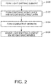
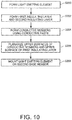
- Fig. 2 is a flowchart showing an example of the method of manufacturing the light emitting device according to the first embodiment.
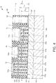
- Fig. 3 through Fig. 5 are cross-sectional views schematically showing a manufacturing process of the light emitting device 100 according to the first embodiment.
- the light emitting element 10 is formed (S100).
- the buffer layer 121 is grown epitaxially on the first base member 110.
- the method of growing the layer epitaxially there can be cited, for example, the metal organic chemical vapor deposition (MOCVD) method, and the molecular beam epitaxy (MBE) method.
- MOCVD metal organic chemical vapor deposition
- MBE molecular beam epitaxy
- the mask layer 122 is formed on the buffer layer 121.
- the mask layer 122 there are formed through holes 122a for forming the first columnar sections 102a, through holes 122b for forming the second columnar sections 102b, and through holes 122c for forming the third columnar sections 102c.
- the diametrical size of the through holes 122a is larger than the diametrical size of the through holes 122b, and the diametrical size of the through holes 122b is larger than the diametrical size of the through holes 122c.
- the first semiconductor layer 124, the light emitting layer 126 and the second semiconductor layer 128 are epitaxially grown on the buffer layer 121 in this order using the MOCVD method, the MBE method or the like using the mask layer 122 as a mask.
- the larger the diametrical size of the through holes 122a, 122b and 122c provided to the mask layer 122 is, the larger the diametrical size of the columnar sections 102a, 102b and 102c formed becomes, and the lower the height becomes.
- first columnar sections 102a having the height H 102a
- second columnar sections 102b having the height H 102b
- third columnar sections 102c having the height H 102c in the same process. Due to the process described above, it is possible to form the stacked body 120 including the columnar sections 102a, 102b and 102c on the first base member 110.
- the mask layer 122 after forming the stacked body 120.
- the light emitting element 10 does not include the mask layer 122.
- the insulating layer 129 is formed between the first columnar sections 102a adjacent to each other, between the second columnar sections 102b adjacent to each other, and between the third columnar sections 102c adjacent to each other, respectively.
- the insulating layer 129 is formed using, for example, a spin coat method or an atomic layer deposition (ALD) method.
- the second electrode 140a is formed on the second semiconductor layer 128 of each of the first columnar sections 102a
- the second electrode 140b is formed on the second semiconductor layer 128 of each of the second columnar sections 102b
- the second electrode 140c is formed on the second semiconductor layer 128 of each of the third columnar sections 102c.
- the first electrode 130 is formed on the buffer layer 121.
- the first electrode 130 and the second electrodes 140a, 140b and 140c are formed using, for example, a vacuum deposition method. It should be noted that the order of forming the first electrode 130 and the second electrodes 140a, 140b and 140c is not particularly limited.
- the light emitting element 10 can be formed.
- the first insulating layer 5 and the second insulating layer 6 are formed on the mask layer 122 (S102).
- the second insulating layer 6 is formed on the mask layer 122.
- the second insulating layer 6 is formed using, for example, a spin coat method, an ALD method, or a chemical vapor deposition (CVD) method.
- the first insulating layer 5 is formed on the second insulating layer 6.
- the opening sections 5a, 5b, 5c and 5d are formed in the first insulating layer 5.
- the second electrodes 140a, 140b and 140c and the first electrode 130 are exposed.
- the first insulating layer 5 functions as a mask when forming the conductive members 8a, 8b, 8c and 8d.
- the first insulating layer 5 is formed by deposition using, for example, the spin coat method, the ALD method, or the CVD method, and patterning using the photolithography technique and the etching technique.
- the deposition of the first insulating layer 5 and the deposition of the second insulating layer 6 can also be performed at the same time.
- the first conductive member 8a is formed on the first columnar sections 102a
- the second conductive member 8b is formed on the second columnar sections 102b
- the third conductive member 8c is formed on the third columnar sections 102c
- the conductive member 8d is formed on the first electrode 130 (S104).
- the conductive members 8a, 8b and 8c are formed on the second electrodes 140a, 140b and 140c, and the conductive member 8d is formed on the first electrode 130 using the first insulating layer 5 as a mask.
- the first conductive member 8a is formed on the second electrode 140a exposed by the first opening section 5a of the first insulating layer 5.
- the second conductive member 8b is formed on the second electrode 140b exposed by the second opening section 5b of the first insulating layer 5.
- the third conductive member 8c is formed on the second electrode 140c exposed by the third opening section 5c of the first insulating layer 5.
- the conductive member 8d is formed on the first electrode 130 exposed by the opening section 5d of the first insulating layer 5.
- the conductive members 8a, 8b, 8c and 8d are formed using, for example, an electrolytic plating method, an electroless plating method, a vacuum deposition method, or a sputtering method. It should be noted that it is also possible to planarize the upper surfaces of the conductive members 8a, 8b, 8c and 8d and the upper surface of the first insulating layer 5 by grinding or a cutting work after forming the conductive members 8a, 8b, 8c and 8d.
- the height H 8b of the second conductive member 8b is made larger than the height H 8a of the first conductive member 8a
- the height H 8c of the third conductive member 8c is made larger than the height H 8b of the second conductive member 8b.
- the light emitting element 10 is mounted on the second base member 20 with the junction-down mounting (S106).
- the second electrode 140a of the first columnar sections 102a and the interconnection 22a of the second base member 20 are electrically connected to each other via the first conductive member 8a.
- the first conductive member 8a and the interconnection 22a are bonded to each other with a bonding member 7 such as solder.
- the second electrode 140b of the second columnar sections 102b and the interconnection 22b of the second base member 20 are electrically connected to each other via the second conductive member 8b.
- the second electrode 140c of the third columnar sections 102c and the interconnection 22c of the second base member 20 are electrically connected to each other via the third conductive member 8c.
- the first electrode 130 and the interconnection 22d of the second base member 20 are electrically connected to each other via the conductive member 8d.
- the bonding member 7 (solder) is firstly formed on the interconnections 22a, 22b, 22c and 22d on the second base member 20 using a printing method or the like. Then, the light emitting element 10 is positioned on the second base member 20 so that the first conductive member 8a is disposed on the interconnection 22a, the second conductive member 8b is disposed on the interconnection 22b, the third conductive member 8c is disposed on the interconnection 22c, and the conductive member 8d is disposed on the interconnection 22d. Then, the bonding member 7 is heated in this state.
- the first conductive member 8a and the interconnection 22a are bonded to each other
- the second conductive member 8b and the interconnection 22b are bonded to each other
- the third conductive member 8c and the interconnection 22c are bonded to each other
- the conductive member 8d and the interconnection 22d are bonded to each other. Due to the process described hereinabove, it is possible to mount the light emitting element 10 on the second base member 20 with the junction-down mounting.
- the light emitting device 100 can be manufactured.
- the method of manufacturing the light emitting device 100 according to the first embodiment has, for example, the following features.
- the method of manufacturing the light emitting device 100 includes the process of forming the stacked body 120 including the first columnar sections 102a having the height H 102a , the second columnar sections 102b having the height H 102b smaller than the height H 102a , and the third columnar sections 102c having the height H 102c smaller than the height H 102b on the first base member 110 to form the light emitting element 10, the process of forming the first conductive member 8a having the height H 8a on the first columnar sections 102a, forming the second conductive member 8b having the height H 8b larger than the height H 8a on the second columnar sections 102b, and forming the third conductive member 8c having the height H 8c larger than the height H 8b on the third columnar sections 102c, and the process of mounting the light emitting element 10 on the second base member 20.
- the first columnar sections 102a and the second base member 20 are electrically connected to each other via the first conductive member 8a
- the second columnar sections 102b and the second base member 20 are electrically connected to each other via the second conductive member 8b
- the third columnar sections 102c and the second base member 20 are electrically connected to each other via the third conductive member 8c.
- the height H 8b of the second conductive member 8b is made larger than the height H 8a of the first conductive member 8a, it is possible to reduce the possibility that the contact failure occurs between the second columnar sections 102b and the second base member 20.
- the height H 8c of the third conductive member 8c is made larger than the height H 8b of the second conductive member 8b, it is possible to reduce the possibility that the contact failure occurs between the third columnar sections 102c and the second base member 20. Therefore, in the method of manufacturing the light emitting device according to the first embodiment, it is possible to enhance the connection stability between the light emitting element 10 and the second base member 20 (the mounting board) .
- the first insulating layer 5 as a mask when forming the conductive members 8a, 8b, 8c and 8d, it is possible to simplify the manufacturing process.
- the first insulating layer 5 is formed, and then the conductive members 8a, 8b, 8c and 8d are formed using the first insulating layer 5 as a mask.
- the first insulating layer 5 is formed after forming the conductive members 8a, 8b, 8c and 8d.
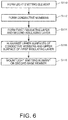
- Fig. 6 is a flowchart showing the modified example of the method of manufacturing the light emitting device according to the first embodiment.
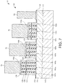
- Fig. 7 and Fig. 8 are cross-sectional views schematically showing the modified example of the manufacturing process of the light emitting device according to the first embodiment.
- the light emitting element 10 is formed (S110).
- the present process S110 is performed in substantially the same manner as the process S100 shown in Fig. 2 described above.
- the conductive members 8a, 8b, 8c and 8d are formed (S112).
- the conductive members 8a, 8b, 8c and 8d are formed using the electrolytic plating method, the electroless plating method, the vacuum deposition method, the sputtering method or the like.
- a mask layer (not shown) is formed, and then the conductive members 8a, 8b, 8c and 8d are formed with the electrolytic plating method or the electroless plating method using the mask layer as a mask.
- a liftoff method for example, is used.
- the first insulating layer 5 and the second insulating layer 6 are formed (S114).
- the second insulating layer 6 is formed on the mask layer 122, and the first insulating layer 5 is formed on the second insulating layer 6.
- the first insulating layer 5 and the second insulating layer 6 are formed using, for example, the spin coat method, the ALD method, or the CVD method.
- the upper surfaces of the conductive members 8a, 8b, 8c and 8d and the upper surface of the first insulating layer 5 are planarized by grinding or the cutting work (S116).
- the height H 8b of the second conductive member 8b is made larger than the height H 8a of the first conductive member 8a
- the height H 8c of the third conductive member 8c is made larger than the height H 8b of the second conductive member 8b.
- the light emitting element 10 is mounted on the second base member 20 (S118).
- the present process S118 is performed in substantially the same manner as the process S106 shown in Fig. 2 described above.
- the light emitting device 100 can be manufactured.
- Fig. 9 is a cross-sectional view schematically showing the light emitting device 200 according to the second embodiment.
- the members having the same functions as those of the constituent members of the light emitting device 100 according to the first embodiment described above will be denoted by the same reference symbols, and detailed description thereof will be omitted.
- the conductive members 8a, 8b and 8c for electrically connecting the second electrodes 140a, 140b and 140c and the interconnections 22a, 22b and 22c of the second base member 20 to each other, and the conductive member 8d for electrically connecting the first electrode 130 and the interconnection 22d of the second base member 20 to each other are each the metal bump formed using the electrolytic plating method, the electroless plating method, or the like.
- the conductive members 208a, 208b and 208c for electrically connecting the second electrodes 140a, 140b and 140c and the interconnections 22a, 22b and 22c of the second base member 20 to each other, and the conductive member 208d for electrically connecting the first electrode 130 and the interconnection 22d of the second base member 20 to each other are each formed using a conductive paste.
- the conductive paste used when forming the conductive members 208a, 208b, 208c and 208d is, for example, a silver paste.
- the silver paste is a paste including nano-sized silver particles or micrometer-sized silver particles. It should be noted that it is also possible to use a metal paste including metal particles other than the silver particles as the conductive members 208a, 208b, 208c and 208d.
- the first insulating layer 5 and the second insulating layer 6 are made of a material having heat resistance enough to withstand the calcination temperature of the conductive paste.
- the height H 208b of the second conductive member 208b is larger than the height H 208a of the first conductive member 208a.
- the height H 208c of the third conductive member 208c is larger than the height H 208b of the second conductive member 208b.
- a sum of the height H 208a of the first conductive member 208a and the height H 102a of the first columnar sections 102a, a sum of the height H 208b of the second conductive member 208b and the height H 102b of the second columnar sections 102b, and a sum of the height H 208c of the third conductive member 208c and the height H 102c of the third columnar sections 102c are equal to each other.
- the heights H 208a , H 208b and H 208c are sizes in the stacking direction of the conductive members 208a, 208b and 208c, respectively.
- the bonding member 7 for bonding the conductive members 8a, 8b, 8c and 8d and the interconnections 22a, 22b, 22c and 22d to each other is solder.
- a bonding member 207 for bonding the conductive members 208a, 208b, 208c and 208d and the interconnections 22a, 22b, 22c and 22d to each other is, for example, formed using a conductive paste.
- the conductive paste used when forming the bonding member 207 and the conductive paste used when forming the conductive members 208a, 208b, 208c and 208d can also be the same material.
- the light emitting device 200 it is possible to exert substantially the same functions and advantages as those of the light emitting device 100 described above.
- Fig. 10 is a flowchart showing an example of the method of manufacturing the light emitting device according to the second embodiment.
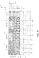
- Fig. 11 is a cross-sectional view schematically showing a manufacturing process of the light emitting device according to the second embodiment.
- the light emitting element 10 is formed (S200).
- the present process S200 is performed in substantially the same manner as the process S100 shown in Fig. 2 described above.
- the first insulating layer 5 and the second insulating layer 6 are formed (S202).
- the present process S202 is performed in substantially the same manner as the process S102 shown in Fig. 2 described above.
- the conductive members 208a, 208b, 208c and 208d are formed using the conductive paste (S204).
- the conductive paste is formed on the second electrode 140a exposed by the first opening section 5a of the first insulating layer 5. Similarly, the conductive paste is formed on the second electrode 140b exposed by the second opening section 5b of the first insulating layer 5. Similarly, the conductive paste is formed on the second electrode 140c exposed by the third opening section 5c of the first insulating layer 5. Similarly, the conductive paste is formed on the first electrode 130 exposed by the opening section 5d of the first insulating layer 5. These conductive pastes are formed at the same time using, for example, the printing method. Then, the conductive pates are calcined. Thus, the conductive members 208a, 208b, 208c and 208d are formed.
- the upper surfaces of the conductive members 208a, 208b, 208c and 208d and the upper surface of the first insulating layer 5 are planarized by grinding or the cutting work (S206).
- the height H 208b of the second conductive member 208b is made larger than the height H 208a of the first conductive member 208a
- the height H 208c of the third conductive member 208c is made larger than the height H 208b of the second conductive member 208b.
- the light emitting element 10 is mounted on the second base member 20 (S208).
- the conductive paste is firstly formed on the interconnections 22a, 22b, 22c and 22d on the second base member 20 using the printing method or the like. Then, the light emitting element 10 is positioned on the second base member 20 so that the first conductive member 208a is disposed on the interconnection 22a, the second conductive member 208b is disposed on the interconnection 22b, the third conductive member 208c is disposed on the interconnection 22c, and the conductive member 208d is disposed on the interconnection 22d. Then, the conductive paste is calcined in this state.
- the first conductive member 208a and the interconnection 22a are bonded to each other with the bonding member 207
- the second conductive member 208b and the interconnection 22b are bonded to each other with the bonding member 207
- the third conductive member 208c and the interconnection 22c are bonded to each other with the bonding member 207
- the conductive member 208d and the interconnection 22d are bonded to each other with the bonding member 207. Due to the process described hereinabove, it is possible to mount the light emitting element 10 on the second base member 20 with the junction-down mounting.
- the light emitting device 200 can be manufactured.
- the conductive members 208a, 208b, 208c and 208d can be formed by printing and then calcining the conductive paste, a plating solution and a vacuum apparatus are not required, and thus, it is possible to simplify the manufacturing process compared to the case of forming the conductive members using, for example, the plating method, the vacuum deposition method or the like.
- the first insulating layer 5 is formed, and then the conductive members 208a, 208b, 208c and 208d are formed using the first insulating layer 5 as a mask.
- the first insulating layer 5 is formed after forming the conductive members 208a, 208b, 208c and 208d.
- Fig. 12 is a flowchart showing the modified example of the method of manufacturing the light emitting device according to the second embodiment.
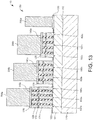
- Fig. 13 and Fig. 14 are cross-sectional views schematically showing the modified example of the manufacturing process of the light emitting device according to the second embodiment.
- the light emitting element 10 is formed (S210).
- the present process S210 is performed in substantially the same manner as the process S200 shown in Fig. 10 described above.
- the conductive members 208a, 208b, 208c and 208d are formed using the conductive paste (S212).
- the conductive paste is formed on the second electrode 140a. Similarly, the conductive paste is formed on the second electrode 140b. Similarly, the conductive paste is formed on the second electrode 140c. Similarly, the conductive paste is formed on the first electrode 130. These conductive pastes are formed at the same time using, for example, the printing method. Then, the conductive pates are calcined. Thus, the conductive members 208a, 208b, 208c and 208d are formed.
- the first insulating layer 5 and the second insulating layer 6 are formed (S214).
- the second insulating layer 6 is formed on the mask layer 122, and the first insulating layer 5 is formed on the second insulating layer 6.
- the first insulating layer 5 and the second insulating layer 6 are formed using, for example, the spin coat method, the ALD method, or the CVD method.
- the upper surfaces of the conductive members 208a, 208b, 208c and 208d and the upper surface of the first insulating layer 5 are planarized by grinding or the cutting work (S216) .
- the height H 208b of the second conductive member 208b is made larger than the height H 208a of the first conductive member 208a
- the height H 208c of the third conductive member 208c is made larger than the height H 208b of the second conductive member 208b.
- the light emitting element 10 is mounted on the second base member 20 (S218).
- the present process S218 is performed in substantially the same manner as the process S208 shown in Fig. 2 described above.
- the light emitting device 200 can be manufactured.
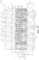
- Fig. 15 is a cross-sectional view schematically showing the light emitting device 300 according to the third embodiment.
- the members having the same functions as those of the constituent members of the light emitting device 100 according to the first embodiment described above will be denoted by the same reference symbols, and detailed description thereof will be omitted.
- the conductive members 8a, 8b and 8c for electrically connecting the second electrodes 140a, 140b and 140c and the interconnections 22a, 22b and 22c of the second base member 20 to each other, and the conductive member 8d for electrically connecting the first electrode 130 and the interconnection 22d of the second base member 20 to each other are each the metal bump formed using the electrolytic plating method, the electroless plating method, or the like.
- the conductive members 308a, 308b and 308c for electrically connecting the second electrodes 140a, 140b and 140c and the interconnections 22a, 22b and 22c of the second base member 20 to each other, and the conductive member 308d for electrically connecting the first electrode 130 and the interconnection 22d of the second base member 20 to each other are each a bump (e.g., a stud bump) to achieve electrical connection by pressing a metal ball.
- the material of the bump used as the conductive members 308a, 308b, 308c and 308d is metal such as gold.
- the height H 308b of the second conductive member 308b is larger than the height H 308a of the first conductive member 308a.
- the height H 308c of the third conductive member 308c is larger than the height H 308b of the second conductive member 308b.
- a sum of the height H 308a of the first conductive member 308a and the height H 102a of the first columnar sections 102a, a sum of the height H 308b of the second conductive member 308b and the height H 102b of the second columnar sections 102b, and a sum of the height H 308c of the third conductive member 308c and the height H 102c of the third columnar sections 102c are equal to each other.
- the heights H 308a , H 308b and H 308c are sizes in the stacking direction of the conductive members 308a, 308b and 308c, respectively.
- the light emitting device 300 it is possible to exert substantially the same functions and advantages as those of the light emitting device 100 described above.
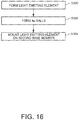
- Fig. 16 is a flowchart showing an example of the method of manufacturing the light emitting device according to the third embodiment.
- Fig. 17 is a cross-sectional view schematically showing a manufacturing process of the light emitting device according to the third embodiment.
- the light emitting element 10 is formed (S300).
- the present process S300 is performed in substantially the same manner as the process S100 shown in Fig. 2 described above.
- the Au ball 301a is formed on the second electrode 140a.
- the Au ball 301b is formed on the second electrode 140b.
- the Au ball 301c is formed on the second electrode 140c.
- the Au ball 301d is formed on the first electrode 130.
- These Au balls 301a, 301b, 301c and 301d are formed using, for example, the technology of wire bonding.
- the Au balls 301a, 301b and 301c are formed to have sizes corresponding to the heights H 102a , H 102b and H 102c of the columnar sections 102a, 102b and 102c, respectively.
- the Au ball 301a is formed to be smaller than the Au ball 301b.
- the Au ball 301b is formed to be smaller than the Au ball 301c.
- the light emitting element 10 is mounted on the second base member 20 (S304).
- the light emitting element 10 is positioned on the second base member 20 so that the Au ball 301a is disposed on the interconnection 22a, the Au ball 301b is disposed on the interconnection 22b, the Au ball 301c is disposed on the interconnection 22c, and the Au ball 301d is disposed on the interconnection 22d. Then, the light emitting element 10 is pressed against the second base member 20 to apply pressure to the Au balls 301a, 301b, 301c and 301d, and at the same time, the Au balls 301a, 301b, 301c and 301d are heated (thermocompression bonding). Thus, the conductive members 308a, 308b, 308c and 308d are formed.
- the first insulating layer 5 and the second insulating layer 6 are formed.
- the first insulating layer 5 and the second insulating layer 6 are made of liquid curable resin (an underfill material) such as epoxy resin.
- liquid curable resin an underfill material
- the first insulating layer 5 and the second insulating layer 6 are formed integrally.
- the light emitting device 300 can be manufactured.
- Fig. 18 is a diagram schematically showing the projector 400 according to the fourth embodiment. It should be noted that in Fig. 18 , a housing for constituting the projector 400 is omitted from the illustration for the sake of convenience.
- the projector 400 includes a light emitting device according to the invention.
- the projector 400 including the light emitting device 100 will be described as shown in Fig. 18 .
- the projector 400 includes the light emitting device 100 and a projection lens 404.
- the light emitting device 100 has a plurality of first light emitting sections 104a for emitting the blue light La, a plurality of second light emitting sections 104b for emitting the green light Lb, a plurality of third light emitting sections 104c for emitting the red light Lc.
- the plurality of first light emitting sections 104a, the plurality of second light emitting sections 104b, and the plurality of third light emitting sections 104c are disposed on the same base member (the first base member 110).
- the light emitting device 100 uses the plurality of first light emitting sections 104a, the plurality of second light emitting sections 104b and the plurality of third light emitting sections 104c as the pixels of the picture, and the plurality of first light emitting sections 104a, the plurality of second light emitting sections 104b and the plurality of third light emitting sections 104c are controlled in accordance with the image information.
- the projector 400 it is possible to directly form the picture without using, for example, liquid crystal light valves (light modulation devices).
- the projection lens 404 enlarges the picture formed by the light emitting device 100, and then projects the picture on the screen (a display surface) not shown.
- the light emitted from the light emitting device 100 directly enters the projection lens 404, and the picture formed by the light emitting device 100 is displayed on the screen (the display surface) in an enlarged manner.
- the projector 400 it is possible to perform full-color image display with a single light emitting device 100.
- the light emitting device 100 there is included the light emitting device 100. Therefore, in the projector 400, it is possible to directly form the picture without using, for example, liquid crystal light valves (light modulation devices) . Therefore, in the projector 400, it is possible to reduce the transmission loss (failure in transmission of a part of the light through the liquid crystal light valves) in the liquid crystal light valves to thereby achieve an increase in luminance. Further, in the projector 400, the number of components can be reduced, and thus, it is possible to achieve the cost reduction.
- liquid crystal light valves light modulation devices
- the light emitting device can also be used as an indoor/outdoor illumination, a backlight for a display, and a light source of a laser printer, a scanner, an in-car light, sensing equipment using light, communication equipment, and so on besides the projector.
- the invention includes configurations (e.g., configurations having the same function, the same way, and the same result, or configurations having the same object and the same advantage) substantially the same as the configuration described as the embodiments of the invention. Further, the invention includes configurations obtained by replacing a non-essential part of the configuration described as the embodiments of the invention. Further, the invention includes configurations providing the same functions and advantages and configurations capable of achieving the same object as the configuration described as the embodiments of the invention. Further, the invention includes configurations obtained by adding known technologies to the configuration described as one of the embodiments of the invention.
Landscapes
- Physics & Mathematics (AREA)
- Optics & Photonics (AREA)
- General Physics & Mathematics (AREA)
- Led Devices (AREA)
- Projection Apparatus (AREA)
- Semiconductor Lasers (AREA)
Abstract
Description
- The present invention relates to a light emitting device, a projector, and a method of manufacturing a light emitting device.
- A light emitting element to which nanostructures (nano columns) are applied gathers attention as a light emitting element such as a semiconductor laser or a light emitting diode. In the light emitting element to which the nanostructures are applied, it is possible to reduce dislocations and defects occurring in a semiconductor layer constituting the light emitting element, and thus, it is possible to obtain a high quality crystal. Therefore, the light emitting element to which the nanostructures are applied can be provided with excellent light emitting characteristics.
- As a mounting method of the light emitting element, there is known junction-down mounting. By mounting the light emitting element using the junction-down mounting, it is possible to efficiently radiate the heat generated in the light emitting element.
- In
JP-A-2009-9978 Document 1, the light emitting element having the nano columns is mounted in the ceramic package using the junction-down mounting. - Here, in the light emitting element to which the nanostructures are applied, it is possible to control the wavelength by changing the diametrical sizes and the pitch of the nanostructures. Therefore, it is possible to emit light beams different in wavelength from each other from the plurality of nanostructures formed on a single substrate, and thus, it is possible to realize the light emitting element performing multicolor emission with the single substrate.
- However, in such a light emitting element, by changing the diametrical sizes and the pitch of the nanostructures formed on the same substrate, the nanostructures become different in height from each other in some cases. Therefore, in the case of mounting such a light emitting element on a mounting board using the junction-down mounting, the gap between the nanostructure low in height and the mounting board becomes larger than the gap between the nanostructure high in height and the mounting board. Thus, the possibility that a contact failure occurs between the nanostructure low in height and the mounting board becomes high.
- An advantage of some aspects of the invention is to provide a light emitting device capable of improving the connection stability between the light emitting element and the mounting board. Another advantage of some aspects of the invention is to provide a method of manufacturing the light emitting device capable of improving the connection stability between the light emitting element and the mounting board. Another advantage of some aspects of the invention is to provide a projector including the light emitting device described above.
- A light emitting device according to an aspect of the invention includes a light emitting element including a first base member, and a stacked body provided to the first base member, and a second base member provided with the light emitting element, the stacked body includes a first semiconductor layer, a second semiconductor layer different in conductivity type from the first semiconductor layer, and a light emitting layer disposed between the first semiconductor layer and the second semiconductor layer, the light emitting layer being capable of emitting light in response to a current injected into the light emitting layer, the stacked body includes a first columnar section having a first height, and a second columnar section having a second height smaller than the first height, the first columnar section and the second base member are electrically connected to each other via a first conductive member between the stacked body and the second base member, the second columnar section and the second base member are electrically connected to each other via a second conductive member between the stacked body and the second base member, the first conductive member has a third height, and the second conductive member has a fourth height larger than the third height.
- In such a light emitting device, since the height of the second conductive member is larger than the height of the first conductive member, it is possible to reduce the possibility that the contact failure occurs between the second columnar section and the second base member. Therefore, in such a light emitting device, it is possible to enhance the connection stability between the light emitting element and the second base member (a mounting board).
- It should be noted that in the descriptions related to the invention, the term "electrically connected" is used in such a phrase as "a specific member (hereinafter referred to as a "member B") "electrically connected" to another specific member (hereinafter referred to as a "member A")." In the descriptions related to the invention, in such a case as this example, the term "electrically connected" is used assuming that the case in which the member A and the member B are electrically connected while having direct contact with each other, and the case in which the member A and the member B are electrically connected to each other via another member are included.
- In the light emitting device according to the aspect of the invention, the first columnar section and the second columnar section may each include the first semiconductor layer, the second semiconductor layer, and the light emitting layer.
- In such a light emitting device, it is possible to obtain the first semiconductor layer, the second semiconductor layer and the light emitting layer with crystal defects and dislocations reduced, and thus, it is possible to realize the light emitting device high in efficiency.
- In the light emitting device according to the aspect of the invention, a first insulating layer may be disposed between the first base member and the second base member, the first conductive member may be disposed in a first opening section provided to the first insulating layer, and the second conductive member may be disposed in a second opening section provided to the first insulating layer.
- In such a light emitting device, it is possible to reduce the possibility that the first conductive member and the second conductive member are electrically shorted to each other.
- In the light emitting device according to the aspect of the invention, a second insulating layer may be disposed between the first columnar section and the second columnar section.
- In such a light emitting device, due to the second insulating layer, it is possible to reduce the diffusion of the light generated in the light emitting layer of the first columnar section and the diffusion of the light generated in the light emitting layer of the second columnar section.
- In the light emitting device according to the aspect of the invention, a wavelength of light emitted by the light emitting layer in the first columnar section and a wavelength of light emitted by the light emitting layer in the second columnar section may be different from each other.
- In such a light emitting device, the multicolor emission can be achieved with a single substrate (the first base member).
- A method of manufacturing a light emitting device according to another aspect of the invention includes forming a stacked body including a first columnar section having a first height and a second columnar section having a section height smaller than the first height on a first base member to form a light emitting element, forming a first conductive member having a third height on the first columnar section, and a second conductive member having a fourth height larger than the third height on the second columnar section, and mounting the light emitting element on a second base member, wherein the stacked body includes a first semiconductor layer, a second semiconductor layer different in conductivity type from the first semiconductor layer, and a light emitting layer disposed between the first semiconductor layer and the second semiconductor layer, the light emitting layer being capable of emitting light in response to a current injected into the light emitting layer, in the mounting the light emitting element on the second base member, the first columnar section and the second base member are electrically connected via the first conductive member between the stacked body and the second base member, and the second columnar section and the second base member are electrically connected to each other via the second conductive member between the stacked body and the second base member.
- In such a method of manufacturing the light emitting device, since the height of the second conductive member is made larger than the height of the first conductive member, it is possible to reduce the possibility that the contact failure occurs between the second columnar section and the second base member. Therefore, in such a method of manufacturing the light emitting device, it is possible to manufacture the light emitting device high in the connection stability between the light emitting element and the second base member.
- It should be noted that in the descriptions related to the invention, in the case of using the term "on" in such a phrase as "a specific object (hereinafter referred to as "D") is formed "on" another specific object (hereinafter referred to as "C")," the term "on" is used assuming that both of the case of forming D directly on C and the case of forming D indirectly on C via another object.
- A projector according to another aspect of the invention includes the light emitting device according to the aspect of the invention.
- In such a projector, it is possible to include the light emitting device according to the aspect of the invention.
- The invention will be described with reference to the accompanying drawings, wherein like numbers reference like elements.
-
Fig. 1 is a cross-sectional view schematically showing a light emitting device according to a first embodiment of the invention. -
Fig. 2 is a flowchart showing an example of a method of manufacturing the light emitting device according to the first embodiment. -
Fig. 3 is a cross-sectional view schematically showing a manufacturing process of the light emitting device according to the first embodiment. -
Fig. 4 is a cross-sectional view schematically showing the manufacturing process of the light emitting device according to the first embodiment. -
Fig. 5 is a cross-sectional view schematically showing the manufacturing process of the light emitting device according to the first embodiment. -
Fig. 6 is a flowchart showing a modified example of the method of manufacturing the light emitting device according to the first embodiment. -
Fig. 7 is a cross-sectional view schematically showing a modified example of the manufacturing process of the light emitting device according to the first embodiment. -
Fig. 8 is a cross-sectional view schematically showing the modified example of the manufacturing process of the light emitting device according to the first embodiment. -
Fig. 9 is a cross-sectional view schematically showing a light emitting device according to a second embodiment of the invention. -
Fig. 10 is a flowchart showing an example of a method of manufacturing the light emitting device according to the second embodiment. -
Fig. 11 is a cross-sectional view schematically showing a manufacturing process of the light emitting device according to the second embodiment. -
Fig. 12 is a flowchart showing a modified example of the method of manufacturing the light emitting device according to the second embodiment. -
Fig. 13 is a cross-sectional view schematically showing a modified example of the manufacturing process of the light emitting device according to the second embodiment. -
Fig. 14 is a cross-sectional view schematically showing the modified example of the manufacturing process of the light emitting device according to the second embodiment. -
Fig. 15 is a cross-sectional view schematically showing a light emitting device according to a third embodiment of the invention. -
Fig. 16 is a flowchart showing an example of a method of manufacturing the light emitting device according to the third embodiment. -
Fig. 17 is a cross-sectional view schematically showing a manufacturing process of the light emitting device according to the third embodiment of the invention. -
Fig. 18 is a diagram schematically showing a projector according to a fourth embodiment of the invention. - Some preferred embodiments of the invention will hereinafter be described in detail with reference to the accompanying drawings. It should be noted that the embodiments described below do not unreasonably limit the contents of the invention as set forth in the appended claims. Further, all of the constituents described hereinafter are not necessarily essential elements of the invention.
- Firstly, a light emitting device according to a first embodiment will be described with reference to the accompanying drawings.
Fig. 1 is a cross-sectional view schematically showing thelight emitting device 100 according to the first embodiment. - As shown in
Fig. 1 , thelight emitting device 100 includes alight emitting element 10 and asecond base member 20 provided with thelight emitting element 10. In thelight emitting device 100, thelight emitting element 10 is mounted on the second base member 20 (a mounting board) using the junction-down mounting. - As shown in
Fig. 1 , thelight emitting element 10 includes afirst base member 110, astacked body 120, afirst electrode 130, andsecond electrodes - The
first base member 110 has, for example, a plate-like shape. Thefirst base member 110 is, for example, a sapphire substrate. Thefirst base member 110 is transparent with respect to light beams La, Lb and Lc generated in light emitting layers 126. Therefore, the light beams La, Lb and Lc generated in light emittinglayers 126 are transmitted through thefirst base member 110 to be emitted to the outside. In other words, thelight emitting device 100 emits the light beams La, Lb and Lc from thefirst base member 110 side. - It should be noted that the
first base member 110 is not limited to the sapphire substrate, but it is also possible to use other ceramics substrates, glass substrates or the like. - The
stacked body 120 is provided to thefirst base member 110. Thestacked body 120 is located between thefirst base member 110 and thesecond base member 20. - The
stacked body 120 is constituted by a plurality of layers stacked on aprincipal surface 112 of thefirst base member 110. Thestacked body 120 includes abuffer layer 121, amask layer 122, afirst semiconductor layer 124, alight emitting layer 126 and asecond semiconductor layer 128. The stacking direction of the stacked body 120 (hereinafter simply referred to as a "stacking direction") is perpendicular to theprincipal surface 112 of thefirst base member 110. - The
buffer layer 121 is provided toprincipal surface 112 of thefirst base member 110. Thebuffer layer 121 is disposed between themask layer 122 and thefirst base member 110, and between thefirst semiconductor layer 124 and thefirst base member 110. Thebuffer layer 121 is, for example, a gallium nitride (GaN) layer of a first conductivity type (e.g., the n-type) . It should be noted that in the present embodiment, thebuffer layer 121 can also be provided with a two-layered structure having an undoped GaN layer and the first conductivity type (e.g., the n-type) GaN layer stacked in this order from the substrate side. - The
mask layer 122 is provided to thebuffer layer 121. Themask layer 122 is disposed between a secondinsulating layer 6 and thebuffer layer 121, and between an insulatinglayer 129 and thebuffer layer 121. Themask layer 122 is, for example, a titanium layer, a titanium oxide layer or a silicon oxide layer. Themask layer 122 is a layer functioning as a mask for selectively growing thefirst semiconductor layer 124, thelight emitting layer 126 and thesecond semiconductor layer 128 on thebuffer layer 121 to formcolumnar sections - The
first semiconductor layer 124 is provided to thebuffer layer 121. Thefirst semiconductor layer 124 is disposed between thebuffer layer 121 and thelight emitting layer 126. Thefirst semiconductor layer 124 is, for example, a GaN layer of a first conductivity type (e.g., the n-type). Thefirst semiconductor layer 124 is, for example, an Si-doped n-type GaN layer. - The
light emitting layer 126 is disposed between thefirst semiconductor layer 124 and the second semiconductor layers 128. Thelight emitting layer 126 includes, for example, indium gallium nitride (InGaN). Thelight emitting layer 126 has a quantum well structure constituted by, for example, at least one GaN layer and at least one InGaN layer. The number of the GaN layers and the number of the InGaN layers constituting thelight emitting layer 126 are not particularly limited. Thelight emitting layer 126 is a layer capable of emitting light in response to injection of an electrical current. - The
second semiconductor layer 128 is disposed between the light emittinglayer 126 and thesecond electrodes second semiconductor layer 128 is a layer different in conductivity type from thefirst semiconductor layer 124. Thesecond semiconductor layer 128 is, for example, a GaN layer of a second conductivity type (e.g., the p-type). Thesecond semiconductor layer 128 is, for example, an Mg-doped p-type GaN layer. The semiconductor layers 124, 128 are each a cladding layer having a function of increasing the light intensity in the vicinity of the light emitting layer 126 (preventing the light from being leaked from the light emitting layer 126). It should be noted that thesecond semiconductor layer 128 can also be provided with a contact layer having ohmic contact with thesecond electrodes - The
stacked body 120 includes a plurality of firstcolumnar sections 102a, a plurality of secondcolumnar sections 102b and a plurality of thirdcolumnar sections 102c. Thecolumnar sections first semiconductor layer 124, thelight emitting layer 126 and thesecond semiconductor layer 128. - The plurality of first
columnar sections 102a constitutes a firstlight emitting section 104a. The plurality of secondcolumnar sections 102b constitutes a secondlight emitting section 104b. The plurality of thirdcolumnar sections 102c constitutes a thirdlight emitting section 104c. - In the first
light emitting section 104a, the p-typesecond semiconductor layer 128, thelight emitting layer 126 with no impurity doped, and the n-typefirst semiconductor layer 124 constitute a pin diode. Each of thefirst semiconductor layer 124 and thesecond semiconductor layer 128 is a layer larger in bandgap than thelight emitting layer 126. When applying a forward bias voltage of the pin diode (when injecting a current) between thefirst electrode 130 and thesecond electrode 140a, recombination of the electron and the hole occurs in thelight emitting layer 126. The recombination causes emission of light. The light generated in thelight emitting layer 126 propagates in a planar direction (a direction perpendicular to the stacking direction) due to the semiconductor layers 124, 128 to form a standing wave in the planar direction in the plurality of firstcolumnar sections 102a to cause laser oscillation receiving a gain in thelight emitting layer 126. Then, the firstlight emitting section 104a emits positive first-order diffracted light and negative first-order diffracted light as the light La (a laser beam) in the stacking direction. The light La is emitted while being transmitted through thefirst base member 110. - Substantially the same as the first
light emitting section 104a also applies to the secondlight emitting section 104b and the thirdlight emitting section 104c. Specifically, in the secondlight emitting section 104b, by applying a voltage between thefirst electrode 130 and thesecond electrode 140b, the light Lb is emitted through thefirst base member 110. Further, in the thirdlight emitting section 104c, by applying a voltage between thefirst electrode 130 and thesecond electrode 140c, the light Lc is emitted through thefirst base member 110. - Although not shown in the drawings, two or more first
light emitting sections 104a can also be disposed. Similarly, two or more secondlight emitting sections 104b can also be disposed. Similarly, two or more thirdlight emitting sections 104c can also be disposed. - The first
columnar sections 102a, the secondcolumnar sections 102b and the thirdcolumnar sections 102c are different in diametrical size from each other. In the example shown in the drawings, the diametrical size of the thirdcolumnar sections 102c is larger than the diametrical size of the secondcolumnar sections 102b. Further, the diametrical size of the secondcolumnar sections 102b is larger than the diametrical size of the firstcolumnar sections 102a. - It should be noted that the "diametrical size" corresponds to the diameter in the case in which the planar shape of each of the
columnar sections columnar sections - By making the first
columnar sections 102a, the secondcolumnar sections 102b and the thirdcolumnar section 102c different in diametrical size from each other as described above, the light emitted by thelight emitting layer 126 in the firstcolumnar sections 102a, the light emitted by thelight emitting layer 126 in the secondcolumnar sections 102b and the light emitted by thelight emitting layer 126 in the thirdcolumnar sections 102c can be made different in wavelength from each other. In other words, the wavelength of the light La emitted from the firstlight emitting section 104a, the wavelength of the light Lb emitted from the secondlight emitting section 104b and the wavelength of the light Lc emitted from the thirdlight emitting section 104c are different from each other. - Further, it is also possible to make the pitch of the first
columnar sections 102a in the firstlight emitting section 104a, the pitch of the secondcolumnar sections 102b in the secondlight emitting section 104b and the pitch of the thirdcolumnar sections 102c in the thirdlight emitting section 104c different from each other. Here, in the firstlight emitting section 104a, the firstcolumnar sections 102a are arranged regularly with predetermined intervals, and the pitch of the firstcolumnar sections 102a denotes the interval between the firstcolumnar sections 102a arranged regularly. The same applies to the pitch of the secondcolumnar sections 102b and the pitch of the thirdcolumnar sections 102c. It is also possible to control the wavelength (the color) of the light emitted from each of thelight emitting sections columnar sections light emitting element 10, it is possible to realize the multicolor emission by controlling the diametrical sizes or the pitches of thecolumnar sections - In the
light emitting element 10, for example, the light La emitted from the firstlight emitting section 104a is blue light, the light Lb emitted from the secondlight emitting section 104b is green light, and the light Lc emitted from the thirdlight emitting section 104c is red light. - Here, in the
light emitting element 10, as described later, thecolumnar sections mask layer 122 as a mask. On this occasion, by making thecolumnar sections columnar sections - Therefore, the first
columnar sections 102a, the secondcolumnar sections 102b and the thirdcolumnar sections 102c are different in height from each other. In the example shown in the drawings, the height H102a of the firstcolumnar sections 102a is larger than the height H102b of the secondcolumnar sections 102b. Further, the height H102b of the secondcolumnar sections 102b is larger than the height H102c of the thirdcolumnar sections 102c. - It should be noted that the height H102a, H102b and H102c is a size in the stacking direction of the
columnar sections columnar sections first semiconductor layer 124, the film thickness of thelight emitting layer 126, and the film thickness of thesecond semiconductor layer 128 in the example shown in the drawings. - The
light emitting sections columnar sections light emitting sections columnar sections - For example, in the case in which the emission efficiency of the third
columnar sections 102c for emitting the red light is lower than the emission efficiency of the firstcolumnar sections 102a for emitting the blue light, the area (i.e., the area of the region in which the plurality of thirdcolumnar sections 102c is formed) of the thirdlight emitting section 104c is made larger than the area (i.e., the area of the region in which the plurality of firstcolumnar sections 102a is formed) of the firstlight emitting section 104a. Thus, it is possible to achieve homogenization of the light intensities of the red light and the blue light emitted from thelight emitting element 10. It should be noted that it is also possible for thelight emitting sections - Between the first
columnar sections 102a adjacent to each other, there is disposed the insulatinglayer 129. The insulatinglayer 129 is embedded between the firstcolumnar sections 102a adjacent to each other. The insulatinglayer 129 is disposed between themask layer 122 and thesecond electrode 140a. The insulatinglayer 129 is, for example, a silicon oxide layer, a silicon oxynitride layer, an aluminum oxide layer, a hafnium oxide layer, a GaN layer and an InGaN layer. The light generated in thelight emitting layer 126 passes through the insulatinglayer 129 to propagate in the planar direction. Similarly, the insulatinglayer 129 is disposed between the secondcolumnar sections 102b adjacent to each other, and between the thirdcolumnar sections 102c adjacent to each other. - The
first electrode 130 is disposed on thebuffer layer 121. Thefirst electrode 130 is disposed between aconductive member 8d and thebuffer layer 121. Thefirst electrode 130 is electrically connected to thefirst semiconductor layer 124. Thefirst electrode 130 and thebuffer layer 121 have ohmic contact with each other. Thefirst electrode 130 is one of the electrodes for injecting the current into thelight emitting layer 126. Thefirst electrode 130 is an electrode common to the firstcolumnar sections 102a (the firstlight emitting section 104a), the secondcolumnar sections 102b (the secondlight emitting section 104b) and the thirdcolumnar sections 102c (the thirdlight emitting section 104c) . As thefirst electrode 130, there is used, for example, a metal layer such as an Au layer or an Ag layer, and what is obtained by stacking a Cr layer, an Ni layer and an Au layer in this order from thebuffer layer 121 side. - The
second electrode 140a is provided to the plurality of firstcolumnar sections 102a. Thesecond electrode 140a is disposed between the plurality of firstcolumnar sections 102a (the second semiconductor layer 128) and the firstconductive member 8a. Thesecond electrode 140a is electrically connected to thesecond semiconductor layer 128. Thesecond electrode 140a is an electrode common to the plurality of firstcolumnar sections 102a. Thesecond electrode 140a and thesecond semiconductor layer 128 have ohmic contact with each other. Thesecond electrode 140a is the other of the electrodes for injecting the current into thelight emitting layer 126 of each of the firstcolumnar sections 102a. - The
second electrode 140b is provided to the plurality of secondcolumnar sections 102b. Thesecond electrode 140b is disposed between the plurality of secondcolumnar sections 102b (the second semiconductor layer 128) and a secondconductive member 8b. Thesecond electrode 140b is electrically connected to thesecond semiconductor layer 128. Thesecond electrode 140b is an electrode common to the plurality of secondcolumnar sections 102b. Thesecond electrode 140b and thesecond semiconductor layer 128 have ohmic contact with each other. Thesecond electrode 140b is the other of the electrodes for injecting the current into thelight emitting layer 126 of each of the secondcolumnar sections 102b. - The
second electrode 140c is provided to the plurality of thirdcolumnar sections 102c. Thesecond electrode 140c is disposed between the plurality of thirdcolumnar sections 102c (the second semiconductor layer 128) and a thirdconductive member 8c. Thesecond electrode 140c is electrically connected to thesecond semiconductor layer 128. Thesecond electrode 140c is an electrode common to the plurality of thirdcolumnar sections 102c. Thesecond electrode 140c and thesecond semiconductor layer 128 have ohmic contact with each other. Thesecond electrode 140c is the other of the electrodes for injecting the current into thelight emitting layer 126 of each of the thirdcolumnar sections 102c. - As the
second electrode second semiconductor layer 128 side, and so on. The material of thefirst electrode 130 and the material of thesecond electrode - In the
light emitting device 100, thelight emitting element 10 is mounted on thesecond base member 20 using the junction-down mounting. In other words, in thelight emitting device 100, thestacked body 120 is connected to thesecond base member 20 on the opposite side to thefirst base member 110 side. - The
second base member 20 is provided with thelight emitting element 10. On thesecond base member 20, there is mounted thelight emitting element 10. Thesecond base member 20 hasinterconnections second base member 20 is a mounting board for mounting thelight emitting element 10. - It is preferable for the thermal expansion coefficient of the
second base member 20 to be approximate to the thermal expansion coefficient of thefirst base member 110. Thus, it is possible to reduce warp of the first base member due to the heat applied when mounting thelight emitting element 10 on thesecond base member 20, and the heat generation when driving thelight emitting element 10, and thus, it is possible to reduce stress applied to thelight emitting element 10. Further, the thermal conductivity of thesecond base member 20 is preferably higher than the thermal conductivity of, for example, thestacked body 120, and is further preferably higher than the thermal conductivity of thefirst base member 110. Further, it is preferable for the thermal capacity of thesecond base member 20 to be higher than the thermal capacity of thefirst base member 110. Thus, it is possible to enhance the heat radiation performance of the heat generated in the light emitting element 10 (the stacked body 120). - As the
second base member 20, there is used, for example, a semiconductor substrate such as an SiC substrate, or a ceramics substrate such as an AlN substrate. The semiconductor material such as SiC and the ceramics material such as AlN are high in thermal conductivity, and at the same time, high in electrical insulation property. Therefore, by using such a substrate as thesecond base member 20, the heat radiation performance of thelight emitting element 10 can be enhanced, and at the same time, insulation of theinterconnections second base member 20. In this case, an insulating layer or the like for insulating theinterconnections - The first
conductive member 8a is a bump for electrically connecting thesecond electrode 140a of the firstcolumnar sections 102a and theinterconnection 22a of thesecond base member 20 to each other. The secondconductive member 8b is a bump for electrically connecting thesecond electrode 140b of the secondcolumnar sections 102b and theinterconnection 22b of thesecond base member 20 to each other. The thirdconductive member 8c is a bump for electrically connecting thesecond electrode 140c of the thirdcolumnar sections 102c and theinterconnection 22c of thesecond base member 20 to each other. Theconductive member 8d is a bump for electrically connecting thefirst electrode 130 and theinterconnection 22d of thesecond base member 20 to each other. - Between the
first base member 110 and thesecond base member 20, the firstcolumnar sections 102a (thesecond electrode 140a) and theinterconnection 22a of thesecond base member 20 are electrically connected to each other via the firstconductive member 8a. Further, the secondcolumnar sections 102b (thesecond electrode 140b) and theinterconnection 22b of thesecond base member 20 are electrically connected to each other via the secondconductive member 8b. Further, the thirdcolumnar sections 102c (thesecond electrode 140c) and theinterconnection 22c of thesecond base member 20 are electrically connected to each other via the thirdconductive member 8c. Further, thefirst electrode 130 and theinterconnection 22d of thesecond base member 20 are electrically connected to each other via theconductive member 8d. - The material of the
conductive members conductive members interconnections bonding member 7, respectively. Thebonding member 7 is, for example, solder. - The height H8b of the second
conductive member 8b is larger than the height H8a of the firstconductive member 8a. The height H8c of the thirdconductive member 8c is larger than the height H8b of the secondconductive member 8b. In the example shown in the drawings, a sum of the height H8a of the firstconductive member 8a and the height H102a of the firstcolumnar sections 102a, a sum of the height H8b of the secondconductive member 8b and the height H102b of the secondcolumnar sections 102b, and a sum of the height H8c of the thirdconductive member 8c and the height H102c of the thirdcolumnar sections 102c are equal to each other. It should be noted that the heights H8a, H8b and H8c are sizes in the stacking direction of theconductive members - Between the
first base member 110 and thesecond base member 20, there are disposed the first insulatinglayer 5 and the second insulatinglayer 6. - The first insulating
layer 5 is disposed between theconductive members layer 5 is provided with afirst opening section 5a, asecond opening section 5b, thethird opening section 5c and theopening section 5d. The openingsections layer 5. In thefirst opening section 5a, there is disposed the firstconductive member 8a. In thesecond opening section 5b, there is disposed the secondconductive member 8b. In thethird opening section 5c, there is disposed the thirdconductive member 8c. In theopening section 5d, there is disposed theconductive member 8d. The material of the first insulatinglayer 5 is, for example, polyimide, ultraviolet curable resin, silicon oxide or silicon nitride. - The second
insulating layer 6 is disposed between the firstcolumnar sections 102a and the secondcolumnar sections 102b, and between the secondcolumnar sections 102b and the thirdcolumnar sections 102c. In other words, the second insulatinglayer 6 is disposed between the firstlight emitting section 104a and the secondlight emitting section 104b, and between the secondlight emitting section 104b and the thirdlight emitting section 104c. The material of the second insulatinglayer 6 is, for example, polyimide, ultraviolet curable resin, silicon oxide or silicon nitride. The material of the first insulatinglayer 5 and the material of the second insulatinglayer 6 can be different from each other, or can also be the same as each other. For example, it is also possible to adopt an inorganic material as the second insulatinglayer 6, and to adopt an organic material as the first insulatinglayer 5. - Between the
first base member 110 and thesecond base member 20, the first insulatinglayer 5 is located closer to thesecond base member 20 than the second insulatinglayer 6. It should be noted that it is also possible for the first insulatinglayer 5 and the second insulatinglayer 6 to be the same layer although not shown in the drawings. In other words, it is also possible that just one insulating layer exists alone between thefirst base member 110 and thesecond base member 20. - It should be noted that the case in which the first
light emitting section 104a, the secondlight emitting section 104b and the thirdlight emitting section 104c are each a semiconductor laser using thecolumnar sections light emitting section 104a, the secondlight emitting section 104b and the thirdlight emitting section 104c to be light emitting elements partially resonating using the nanostructures, or the light emitting diodes (LED) using the nanostructures. - The
light emitting device 100 has, for example, the following features. - In the
light emitting device 100, thestacked body 120 includes the firstcolumnar sections 102a having the height H102a, the secondcolumnar sections 102b having the height H102b smaller than the height H102a, and the thirdcolumnar sections 102c having the height H102c smaller than the height H102b. Further, between thestacked body 120 and thesecond base member 20, the firstcolumnar sections 102a and thesecond base member 20 are electrically connected to each other via the firstconductive member 8a, the secondcolumnar sections 102b and thesecond base member 20 are electrically connected to each other via the secondconductive member 8b, and the thirdcolumnar sections 102c and thesecond base member 20 are electrically connected to each other via the thirdconductive member 8c. Further, the height H8c of the thirdconductive member 8c is larger than the height H8b of the secondconductive member 8b, and the height H8b of the secondconductive member 8b is larger than the height H8a of the firstconductive member 8a. - As described above, in the
light emitting device 100, since the height H8b of the secondconductive member 8b is larger than the height H8a of the firstconductive member 8a, it is possible to reduce the possibility that the contact failure occurs between the secondcolumnar sections 102b and thesecond base member 20. Further, since the height H8c of the thirdconductive member 8c is larger than the height H8b of the secondconductive member 8b, it is possible to reduce the possibility that the contact failure occurs between the thirdcolumnar sections 102c and thesecond base member 20. Therefore, in thelight emitting device 100, it is possible to enhance the connection stability between the light emittingelement 10 and the second base member 20 (the mounting board). - Further, in the
light emitting device 100, it is possible to mount thelight emitting element 10 horizontally with respect to thesecond base member 20. For example, in the case in which the heights H102a, H102b and H102c of the respectivecolumnar sections conductive members light emitting element 10 is mounted obliquely with respect to thesecond base member 20. In contrast, in thelight emitting device 100, since the height H8c of the thirdconductive member 8c is larger than the height H8b of the secondconductive member 8b, and the height H8b of the secondconductive member 8b is larger than the height H8a of the firstconductive member 8a, it is possible to decrease the tilt of thelight emitting element 10 with respect to thesecond base member 20 compared to the case in which the heights of theconductive members - In the
light emitting device 100, the firstcolumnar sections 102a, the secondcolumnar sections 102b and the thirdcolumnar sections 102c each include thefirst semiconductor layer 124, thesecond semiconductor layer 128 and thelight emitting layer 126. Therefore, in thelight emitting device 100, it is possible to obtain thefirst semiconductor layer 124, thesecond semiconductor layer 128 and thelight emitting layer 126 with crystal defects and dislocations reduced, and thus, it is possible to realize thelight emitting element 10 high in efficiency. - In the
light emitting device 100, the first insulatinglayer 5 is disposed between thefirst base member 110 and thesecond base member 20, the firstconductive member 8a is disposed in thefirst opening section 5a provided to the first insulatinglayer 5, the secondconductive member 8b is disposed in thesecond opening section 5b provided to the first insulatinglayer 5, and the thirdconductive member 8c is disposed in thethird opening section 5c provided to the first insulatinglayer 5. Therefore, in thelight emitting device 100, it is possible to reduce the possibility that theconductive members - In the
light emitting device 100, the second insulatinglayer 6 is disposed between the firstcolumnar sections 102a and the secondcolumnar sections 102b, and between the secondcolumnar sections 102b and the thirdcolumnar sections 102c. Therefore, in thelight emitting device 100, it is possible to reduce the diffusion of the light generated in thecolumnar sections layer 6. It should be noted that it is preferable for the second insulatinglayer 6 to have the lower refractive index than the refractive index of GaN or InGaN. - In the
light emitting device 100, the wavelength of the light emitted by thelight emitting layer 126 in the firstcolumnar sections 102a, the wavelength of the light emitted by thelight emitting layer 126 in the secondcolumnar sections 102b, and the wavelength of the light emitted by thelight emitting layer 126 in the thirdcolumnar sections 102c are different from each other. Therefore, in thelight emitting device 100, the multicolor emission can be achieved with a single substrate (the first base member 110). - Then, a method of manufacturing the
light emitting device 100 according to the first embodiment will be described with reference to the accompanying drawings.Fig. 2 is a flowchart showing an example of the method of manufacturing the light emitting device according to the first embodiment.Fig. 3 through Fig. 5 are cross-sectional views schematically showing a manufacturing process of thelight emitting device 100 according to the first embodiment. - Firstly, as shown in
Fig. 3 , thelight emitting element 10 is formed (S100). - Specifically, firstly, as shown in
Fig. 3 , thebuffer layer 121 is grown epitaxially on thefirst base member 110. As the method of growing the layer epitaxially, there can be cited, for example, the metal organic chemical vapor deposition (MOCVD) method, and the molecular beam epitaxy (MBE) method. - Then, the
mask layer 122 is formed on thebuffer layer 121. In themask layer 122, there are formed throughholes 122a for forming the firstcolumnar sections 102a, throughholes 122b for forming the secondcolumnar sections 102b, and throughholes 122c for forming the thirdcolumnar sections 102c. The diametrical size of the throughholes 122a is larger than the diametrical size of the throughholes 122b, and the diametrical size of the throughholes 122b is larger than the diametrical size of the throughholes 122c. By the throughholes mask layer 122, thebuffer layer 121 is exposed. Themask layer 122 is formed by deposition using the MOCVD method, the MBE method, or the like, and patterning with a photolithography technique and an etching technique. - Then, the
first semiconductor layer 124, thelight emitting layer 126 and thesecond semiconductor layer 128 are epitaxially grown on thebuffer layer 121 in this order using the MOCVD method, the MBE method or the like using themask layer 122 as a mask. Here, the larger the diametrical size of the throughholes mask layer 122 is, the larger the diametrical size of thecolumnar sections columnar sections 102a having the height H102a, the secondcolumnar sections 102b having the height H102b, and the thirdcolumnar sections 102c having the height H102c in the same process. Due to the process described above, it is possible to form thestacked body 120 including thecolumnar sections first base member 110. - It should be noted that it is also possible to remove the
mask layer 122 after forming thestacked body 120. In this case, thelight emitting element 10 does not include themask layer 122. - Then, the insulating
layer 129 is formed between the firstcolumnar sections 102a adjacent to each other, between the secondcolumnar sections 102b adjacent to each other, and between the thirdcolumnar sections 102c adjacent to each other, respectively. The insulatinglayer 129 is formed using, for example, a spin coat method or an atomic layer deposition (ALD) method. - Then, the
second electrode 140a is formed on thesecond semiconductor layer 128 of each of the firstcolumnar sections 102a, thesecond electrode 140b is formed on thesecond semiconductor layer 128 of each of the secondcolumnar sections 102b, thesecond electrode 140c is formed on thesecond semiconductor layer 128 of each of the thirdcolumnar sections 102c. - Then, the
first electrode 130 is formed on thebuffer layer 121. Thefirst electrode 130 and thesecond electrodes first electrode 130 and thesecond electrodes - According to the process described hereinabove, the
light emitting element 10 can be formed. - Then, as shown in
Fig. 4 , the first insulatinglayer 5 and the second insulatinglayer 6 are formed on the mask layer 122 (S102). - Specifically, firstly, the second insulating
layer 6 is formed on themask layer 122. The secondinsulating layer 6 is formed using, for example, a spin coat method, an ALD method, or a chemical vapor deposition (CVD) method. Then, the first insulatinglayer 5 is formed on the second insulatinglayer 6. The openingsections layer 5. By forming the openingsections second electrodes first electrode 130 are exposed. The first insulatinglayer 5 functions as a mask when forming theconductive members layer 5 is formed by deposition using, for example, the spin coat method, the ALD method, or the CVD method, and patterning using the photolithography technique and the etching technique. - It should be noted that in the case in which the material of the first insulating
layer 5 and the material of the second insulatinglayer 6 are the same, the deposition of the first insulatinglayer 5 and the deposition of the second insulatinglayer 6 can also be performed at the same time. - Then, as shown in
Fig. 5 , the firstconductive member 8a is formed on the firstcolumnar sections 102a, the secondconductive member 8b is formed on the secondcolumnar sections 102b, and the thirdconductive member 8c is formed on the thirdcolumnar sections 102c, and theconductive member 8d is formed on the first electrode 130 (S104). - Specifically, the
conductive members second electrodes conductive member 8d is formed on thefirst electrode 130 using the first insulatinglayer 5 as a mask. In other words, the firstconductive member 8a is formed on thesecond electrode 140a exposed by thefirst opening section 5a of the first insulatinglayer 5. Similarly, the secondconductive member 8b is formed on thesecond electrode 140b exposed by thesecond opening section 5b of the first insulatinglayer 5. Similarly, the thirdconductive member 8c is formed on thesecond electrode 140c exposed by thethird opening section 5c of the first insulatinglayer 5. Similarly, theconductive member 8d is formed on thefirst electrode 130 exposed by theopening section 5d of the first insulatinglayer 5. Theconductive members conductive members layer 5 by grinding or a cutting work after forming theconductive members - Due to the present process, the height H8b of the second
conductive member 8b is made larger than the height H8a of the firstconductive member 8a, and the height H8c of the thirdconductive member 8c is made larger than the height H8b of the secondconductive member 8b. - Then, as shown in
Fig. 1 , thelight emitting element 10 is mounted on thesecond base member 20 with the junction-down mounting (S106). - Specifically, between the
stacked body 120 and thesecond base member 20, thesecond electrode 140a of the firstcolumnar sections 102a and theinterconnection 22a of thesecond base member 20 are electrically connected to each other via the firstconductive member 8a. The firstconductive member 8a and theinterconnection 22a are bonded to each other with abonding member 7 such as solder. Similarly, between thestacked body 120 and thesecond base member 20, thesecond electrode 140b of the secondcolumnar sections 102b and theinterconnection 22b of thesecond base member 20 are electrically connected to each other via the secondconductive member 8b. Similarly, between thestacked body 120 and thesecond base member 20, thesecond electrode 140c of the thirdcolumnar sections 102c and theinterconnection 22c of thesecond base member 20 are electrically connected to each other via the thirdconductive member 8c. Similarly, between thefirst base member 110 and thesecond base member 20, thefirst electrode 130 and theinterconnection 22d of thesecond base member 20 are electrically connected to each other via theconductive member 8d. - More specifically, for example, the bonding member 7 (solder) is firstly formed on the
interconnections second base member 20 using a printing method or the like. Then, thelight emitting element 10 is positioned on thesecond base member 20 so that the firstconductive member 8a is disposed on theinterconnection 22a, the secondconductive member 8b is disposed on theinterconnection 22b, the thirdconductive member 8c is disposed on theinterconnection 22c, and theconductive member 8d is disposed on theinterconnection 22d. Then, thebonding member 7 is heated in this state. Thus, the firstconductive member 8a and theinterconnection 22a are bonded to each other, the secondconductive member 8b and theinterconnection 22b are bonded to each other, the thirdconductive member 8c and theinterconnection 22c are bonded to each other, and theconductive member 8d and theinterconnection 22d are bonded to each other. Due to the process described hereinabove, it is possible to mount thelight emitting element 10 on thesecond base member 20 with the junction-down mounting. - According to the process described hereinabove, the
light emitting device 100 can be manufactured. - The method of manufacturing the
light emitting device 100 according to the first embodiment has, for example, the following features. - The method of manufacturing the
light emitting device 100 according to the first embodiment includes the process of forming thestacked body 120 including the firstcolumnar sections 102a having the height H102a, the secondcolumnar sections 102b having the height H102b smaller than the height H102a, and the thirdcolumnar sections 102c having the height H102c smaller than the height H102b on thefirst base member 110 to form thelight emitting element 10, the process of forming the firstconductive member 8a having the height H8a on the firstcolumnar sections 102a, forming the secondconductive member 8b having the height H8b larger than the height H8a on the secondcolumnar sections 102b, and forming the thirdconductive member 8c having the height H8c larger than the height H8b on the thirdcolumnar sections 102c, and the process of mounting thelight emitting element 10 on thesecond base member 20. Further, in the process of mounting thelight emitting element 10 on thesecond base member 20, between thestacked body 120 and thesecond base member 20, the firstcolumnar sections 102a and thesecond base member 20 are electrically connected to each other via the firstconductive member 8a, the secondcolumnar sections 102b and thesecond base member 20 are electrically connected to each other via the secondconductive member 8b, and the thirdcolumnar sections 102c and thesecond base member 20 are electrically connected to each other via the thirdconductive member 8c. - As described above, in the method of manufacturing the light emitting device according to the first embodiment, since the height H8b of the second
conductive member 8b is made larger than the height H8a of the firstconductive member 8a, it is possible to reduce the possibility that the contact failure occurs between the secondcolumnar sections 102b and thesecond base member 20. Further, since the height H8c of the thirdconductive member 8c is made larger than the height H8b of the secondconductive member 8b, it is possible to reduce the possibility that the contact failure occurs between the thirdcolumnar sections 102c and thesecond base member 20. Therefore, in the method of manufacturing the light emitting device according to the first embodiment, it is possible to enhance the connection stability between the light emittingelement 10 and the second base member 20 (the mounting board) . - Further, in the method of manufacturing the light emitting device according to the first embodiment, since it is possible to use the first insulating
layer 5 as a mask when forming theconductive members - Then, a modified example of the method of manufacturing the
light emitting device 100 according to the first embodiment will be described. In the embodiment described above, the first insulatinglayer 5 is formed, and then theconductive members layer 5 as a mask. In contrast, in the present modified example, the first insulatinglayer 5 is formed after forming theconductive members Fig. 2 described above will be explained, and the description of similarities will be omitted. -
Fig. 6 is a flowchart showing the modified example of the method of manufacturing the light emitting device according to the first embodiment.Fig. 7 andFig. 8 are cross-sectional views schematically showing the modified example of the manufacturing process of the light emitting device according to the first embodiment. - Firstly, as shown in
Fig. 3 , thelight emitting element 10 is formed (S110). - The present process S110 is performed in substantially the same manner as the process S100 shown in
Fig. 2 described above. - Then, as shown in
Fig. 7 , theconductive members - The
conductive members conductive members conductive members conductive members - Then, as shown in
Fig. 8 , the first insulatinglayer 5 and the second insulatinglayer 6 are formed (S114). - Specifically, the second insulating
layer 6 is formed on themask layer 122, and the first insulatinglayer 5 is formed on the second insulatinglayer 6. The first insulatinglayer 5 and the second insulatinglayer 6 are formed using, for example, the spin coat method, the ALD method, or the CVD method. - Then, as shown in
Fig. 5 , the upper surfaces of theconductive members layer 5 are planarized by grinding or the cutting work (S116). Thus, the height H8b of the secondconductive member 8b is made larger than the height H8a of the firstconductive member 8a, and the height H8c of the thirdconductive member 8c is made larger than the height H8b of the secondconductive member 8b. - Then, as shown in
Fig. 1 , thelight emitting element 10 is mounted on the second base member 20 (S118). - The present process S118 is performed in substantially the same manner as the process S106 shown in
Fig. 2 described above. - According to the process described hereinabove, the
light emitting device 100 can be manufactured. - In the method of manufacturing the light emitting device according to the present modified example, it is possible to exert substantially the same functions and advantages as those of the method of manufacturing the light emitting device according to the first embodiment described above.
- Then, a light emitting device according to a second embodiment will be described with reference to the accompanying drawings.
Fig. 9 is a cross-sectional view schematically showing thelight emitting device 200 according to the second embodiment. Hereinafter, in thelight emitting device 200 according to the second embodiment, the members having the same functions as those of the constituent members of thelight emitting device 100 according to the first embodiment described above will be denoted by the same reference symbols, and detailed description thereof will be omitted. - In the
light emitting device 100 described above, theconductive members second electrodes interconnections second base member 20 to each other, and theconductive member 8d for electrically connecting thefirst electrode 130 and theinterconnection 22d of thesecond base member 20 to each other are each the metal bump formed using the electrolytic plating method, the electroless plating method, or the like. - In contrast, in the
light emitting device 200, theconductive members second electrodes interconnections second base member 20 to each other, and theconductive member 208d for electrically connecting thefirst electrode 130 and theinterconnection 22d of thesecond base member 20 to each other are each formed using a conductive paste. - The conductive paste used when forming the
conductive members conductive members - It should be noted that in the case of forming the
conductive members layer 5 and the second insulatinglayer 6 to be made of a material having heat resistance enough to withstand the calcination temperature of the conductive paste. - The height H208b of the second
conductive member 208b is larger than the height H208a of the firstconductive member 208a. The height H208c of the thirdconductive member 208c is larger than the height H208b of the secondconductive member 208b. In the example shown in the drawings, a sum of the height H208a of the firstconductive member 208a and the height H102a of the firstcolumnar sections 102a, a sum of the height H208b of the secondconductive member 208b and the height H102b of the secondcolumnar sections 102b, and a sum of the height H208c of the thirdconductive member 208c and the height H102c of the thirdcolumnar sections 102c are equal to each other. It should be noted that the heights H208a, H208b and H208c are sizes in the stacking direction of theconductive members - Further, in the
light emitting device 100 described above, thebonding member 7 for bonding theconductive members interconnections - In contrast, in the
light emitting device 200, abonding member 207 for bonding theconductive members interconnections bonding member 207 and the conductive paste used when forming theconductive members - In the
light emitting device 200, it is possible to exert substantially the same functions and advantages as those of thelight emitting device 100 described above. - Then, a method of manufacturing the light emitting device according to the second embodiment will be described with reference to the accompanying drawings.
Fig. 10 is a flowchart showing an example of the method of manufacturing the light emitting device according to the second embodiment.Fig. 11 is a cross-sectional view schematically showing a manufacturing process of the light emitting device according to the second embodiment. Hereinafter, differences from the method of manufacturing the light emitting device according to the first embodiment shown inFig. 2 described above will be explained, and the description of similarities will be omitted. - Firstly, as shown in
Fig. 3 , thelight emitting element 10 is formed (S200). - The present process S200 is performed in substantially the same manner as the process S100 shown in
Fig. 2 described above. - Then, as shown in
Fig. 11 , the first insulatinglayer 5 and the second insulatinglayer 6 are formed (S202). - The present process S202 is performed in substantially the same manner as the process S102 shown in
Fig. 2 described above. - Then, the
conductive members - Specifically, the conductive paste is formed on the
second electrode 140a exposed by thefirst opening section 5a of the first insulatinglayer 5. Similarly, the conductive paste is formed on thesecond electrode 140b exposed by thesecond opening section 5b of the first insulatinglayer 5. Similarly, the conductive paste is formed on thesecond electrode 140c exposed by thethird opening section 5c of the first insulatinglayer 5. Similarly, the conductive paste is formed on thefirst electrode 130 exposed by theopening section 5d of the first insulatinglayer 5. These conductive pastes are formed at the same time using, for example, the printing method. Then, the conductive pates are calcined. Thus, theconductive members - Then, the upper surfaces of the
conductive members layer 5 are planarized by grinding or the cutting work (S206). Thus, the height H208b of the secondconductive member 208b is made larger than the height H208a of the firstconductive member 208a, and the height H208c of the thirdconductive member 208c is made larger than the height H208b of the secondconductive member 208b. - Then, the
light emitting element 10 is mounted on the second base member 20 (S208). - Specifically, as shown in
Fig. 9 , the conductive paste is firstly formed on theinterconnections second base member 20 using the printing method or the like. Then, thelight emitting element 10 is positioned on thesecond base member 20 so that the firstconductive member 208a is disposed on theinterconnection 22a, the secondconductive member 208b is disposed on theinterconnection 22b, the thirdconductive member 208c is disposed on theinterconnection 22c, and theconductive member 208d is disposed on theinterconnection 22d. Then, the conductive paste is calcined in this state. Thus, the firstconductive member 208a and theinterconnection 22a are bonded to each other with thebonding member 207, the secondconductive member 208b and theinterconnection 22b are bonded to each other with thebonding member 207, the thirdconductive member 208c and theinterconnection 22c are bonded to each other with thebonding member 207, and theconductive member 208d and theinterconnection 22d are bonded to each other with thebonding member 207. Due to the process described hereinabove, it is possible to mount thelight emitting element 10 on thesecond base member 20 with the junction-down mounting. - According to the process described hereinabove, the
light emitting device 200 can be manufactured. - In the method of manufacturing the light emitting device according to the second embodiment, since the
conductive members - Then, a modified example of the method of manufacturing the light emitting device according to the second embodiment will be described. The modified example of the method of manufacturing the light emitting device according to the first embodiment explained in "1.3. Modified Example" described above can also be applied to the method of manufacturing the light emitting device according to the second embodiment.
- Specifically, in the second embodiment described above, the first insulating
layer 5 is formed, and then theconductive members layer 5 as a mask. In contrast, in the present modified example, the first insulatinglayer 5 is formed after forming theconductive members -
Fig. 12 is a flowchart showing the modified example of the method of manufacturing the light emitting device according to the second embodiment.Fig. 13 andFig. 14 are cross-sectional views schematically showing the modified example of the manufacturing process of the light emitting device according to the second embodiment. - Firstly, as shown in
Fig. 3 , thelight emitting element 10 is formed (S210). - The present process S210 is performed in substantially the same manner as the process S200 shown in
Fig. 10 described above. - Then, as shown in
Fig. 13 , theconductive members - Specifically, firstly, the conductive paste is formed on the
second electrode 140a. Similarly, the conductive paste is formed on thesecond electrode 140b. Similarly, the conductive paste is formed on thesecond electrode 140c. Similarly, the conductive paste is formed on thefirst electrode 130. These conductive pastes are formed at the same time using, for example, the printing method. Then, the conductive pates are calcined. Thus, theconductive members - Then, as shown in
Fig. 14 , the first insulatinglayer 5 and the second insulatinglayer 6 are formed (S214). - Specifically, the second insulating
layer 6 is formed on themask layer 122, and the first insulatinglayer 5 is formed on the second insulatinglayer 6. The first insulatinglayer 5 and the second insulatinglayer 6 are formed using, for example, the spin coat method, the ALD method, or the CVD method. - Then, as shown in
Fig. 11 , the upper surfaces of theconductive members layer 5 are planarized by grinding or the cutting work (S216) . Thus, the height H208b of the secondconductive member 208b is made larger than the height H208a of the firstconductive member 208a, and the height H208c of the thirdconductive member 208c is made larger than the height H208b of the secondconductive member 208b. - Then, as shown in
Fig. 9 , thelight emitting element 10 is mounted on the second base member 20 (S218). - The present process S218 is performed in substantially the same manner as the process S208 shown in
Fig. 2 described above. - According to the process described hereinabove, the
light emitting device 200 can be manufactured. - In the method of manufacturing the light emitting device according to the present modified example, it is possible to exert substantially the same functions and advantages as those of the method of manufacturing the light emitting device according to the second embodiment described above.
- Then, a light emitting device according to a third embodiment will be described with reference to the accompanying drawings.
Fig. 15 is a cross-sectional view schematically showing thelight emitting device 300 according to the third embodiment. Hereinafter, in thelight emitting device 300 according to the third embodiment, the members having the same functions as those of the constituent members of thelight emitting device 100 according to the first embodiment described above will be denoted by the same reference symbols, and detailed description thereof will be omitted. - In the
light emitting device 100 described above, theconductive members second electrodes interconnections second base member 20 to each other, and theconductive member 8d for electrically connecting thefirst electrode 130 and theinterconnection 22d of thesecond base member 20 to each other are each the metal bump formed using the electrolytic plating method, the electroless plating method, or the like. - In contrast, in the
light emitting device 300, theconductive members second electrodes interconnections second base member 20 to each other, and theconductive member 308d for electrically connecting thefirst electrode 130 and theinterconnection 22d of thesecond base member 20 to each other are each a bump (e.g., a stud bump) to achieve electrical connection by pressing a metal ball. The material of the bump used as theconductive members - The height H308b of the second conductive member 308b is larger than the height H308a of the first
conductive member 308a. The height H308c of the thirdconductive member 308c is larger than the height H308b of the second conductive member 308b. In the example shown in the drawings, a sum of the height H308a of the firstconductive member 308a and the height H102a of the firstcolumnar sections 102a, a sum of the height H308b of the second conductive member 308b and the height H102b of the secondcolumnar sections 102b, and a sum of the height H308c of the thirdconductive member 308c and the height H102c of the thirdcolumnar sections 102c are equal to each other. It should be noted that the heights H308a, H308b and H308c are sizes in the stacking direction of theconductive members - In the
light emitting device 300, it is possible to exert substantially the same functions and advantages as those of thelight emitting device 100 described above. - Then, a method of manufacturing the light emitting device according to the third embodiment will be described with reference to the accompanying drawings.
Fig. 16 is a flowchart showing an example of the method of manufacturing the light emitting device according to the third embodiment.Fig. 17 is a cross-sectional view schematically showing a manufacturing process of the light emitting device according to the third embodiment. Hereinafter, differences from the method of manufacturing the light emitting device according to the first embodiment shown inFig. 2 described above will be explained, and the description of similarities will be omitted. - Firstly, as shown in
Fig. 3 , thelight emitting element 10 is formed (S300). - The present process S300 is performed in substantially the same manner as the process S100 shown in
Fig. 2 described above. - Then, as shown in
Fig. 17 ,Au balls - Specifically, firstly, the
Au ball 301a is formed on thesecond electrode 140a. Similarly, theAu ball 301b is formed on thesecond electrode 140b. Similarly, theAu ball 301c is formed on thesecond electrode 140c. Similarly, theAu ball 301d is formed on thefirst electrode 130. TheseAu balls - On this occasion, the
Au balls columnar sections light emitting element 10, since the height H102a of the firstcolumnar sections 102a is larger than the height H102b of the secondcolumnar sections 102b, theAu ball 301a is formed to be smaller than theAu ball 301b. Further, since the height H102b of the secondcolumnar sections 102b is larger than the height H102c of the thirdcolumnar sections 102c, theAu ball 301b is formed to be smaller than theAu ball 301c. Thus, it is possible to reduce the possibility of occurrence of the contact failure. - Then, as shown in
Fig. 15 , thelight emitting element 10 is mounted on the second base member 20 (S304). - Specifically, the
light emitting element 10 is positioned on thesecond base member 20 so that theAu ball 301a is disposed on theinterconnection 22a, theAu ball 301b is disposed on theinterconnection 22b, theAu ball 301c is disposed on theinterconnection 22c, and theAu ball 301d is disposed on theinterconnection 22d. Then, thelight emitting element 10 is pressed against thesecond base member 20 to apply pressure to theAu balls Au balls conductive members - Then, the first insulating
layer 5 and the second insulatinglayer 6 are formed. The first insulatinglayer 5 and the second insulatinglayer 6 are made of liquid curable resin (an underfill material) such as epoxy resin. By supplying the liquid curable resin between thestacked body 120 and thesecond base member 20 and then making the liquid curable resin cure, it is possible to form the first insulatinglayer 5 and the second insulatinglayer 6. In this case, the first insulatinglayer 5 and the second insulatinglayer 6 are formed integrally. - Due to the process described hereinabove, it is possible to mount the
light emitting element 10 on thesecond base member 20 with the junction-down mounting. - It should be noted that it is also possible to form the second insulating
layer 6 before the process S304 of mounting thelight emitting element 10 on thesecond base member 20, and then, form the first insulatinglayer 5 in the process S304 of mounting thelight emitting element 10 on thesecond base member 20. - According to the process described hereinabove, the
light emitting device 300 can be manufactured. - Then, a projector according to a fourth embodiment will be described with reference to the accompanying drawings.
Fig. 18 is a diagram schematically showing theprojector 400 according to the fourth embodiment. It should be noted that inFig. 18 , a housing for constituting theprojector 400 is omitted from the illustration for the sake of convenience. - The
projector 400 includes a light emitting device according to the invention. Hereinafter, theprojector 400 including thelight emitting device 100 will be described as shown inFig. 18 . - As shown in
Fig. 18 , theprojector 400 includes thelight emitting device 100 and aprojection lens 404. - The
light emitting device 100 has a plurality of firstlight emitting sections 104a for emitting the blue light La, a plurality of secondlight emitting sections 104b for emitting the green light Lb, a plurality of thirdlight emitting sections 104c for emitting the red light Lc. The plurality of firstlight emitting sections 104a, the plurality of secondlight emitting sections 104b, and the plurality of thirdlight emitting sections 104c are disposed on the same base member (the first base member 110). - The
light emitting device 100 uses the plurality of firstlight emitting sections 104a, the plurality of secondlight emitting sections 104b and the plurality of thirdlight emitting sections 104c as the pixels of the picture, and the plurality of firstlight emitting sections 104a, the plurality of secondlight emitting sections 104b and the plurality of thirdlight emitting sections 104c are controlled in accordance with the image information. Thus, in theprojector 400, it is possible to directly form the picture without using, for example, liquid crystal light valves (light modulation devices). - The
projection lens 404 enlarges the picture formed by thelight emitting device 100, and then projects the picture on the screen (a display surface) not shown. - In the
projector 400, the light emitted from thelight emitting device 100 directly enters theprojection lens 404, and the picture formed by thelight emitting device 100 is displayed on the screen (the display surface) in an enlarged manner. As described above, in theprojector 400, it is possible to perform full-color image display with a singlelight emitting device 100. - In the
projector 400, there is included thelight emitting device 100. Therefore, in theprojector 400, it is possible to directly form the picture without using, for example, liquid crystal light valves (light modulation devices) . Therefore, in theprojector 400, it is possible to reduce the transmission loss (failure in transmission of a part of the light through the liquid crystal light valves) in the liquid crystal light valves to thereby achieve an increase in luminance. Further, in theprojector 400, the number of components can be reduced, and thus, it is possible to achieve the cost reduction. - The purpose of the light emitting device according to the invention is not limited to the embodiments described above, but the light emitting device can also be used as an indoor/outdoor illumination, a backlight for a display, and a light source of a laser printer, a scanner, an in-car light, sensing equipment using light, communication equipment, and so on besides the projector.
- The invention can be implemented with some of the constituents omitted, or any of the embodiments and the modified examples combined with each other as long as the features and the advantages described in the specification are provided.
- The invention includes configurations (e.g., configurations having the same function, the same way, and the same result, or configurations having the same object and the same advantage) substantially the same as the configuration described as the embodiments of the invention. Further, the invention includes configurations obtained by replacing a non-essential part of the configuration described as the embodiments of the invention. Further, the invention includes configurations providing the same functions and advantages and configurations capable of achieving the same object as the configuration described as the embodiments of the invention. Further, the invention includes configurations obtained by adding known technologies to the configuration described as one of the embodiments of the invention.
Claims (9)
- A light emitting device comprising:a light emitting element including a first base member, and a stacked body provided to the first base member; anda second base member provided with the light emitting element,wherein the stacked body is located between the first base member and the second base member,the stacked body includesa first columnar section having a first height, anda second columnar section having a second height smaller than the first height,the first columnar section and the second columnar section respectively includea first semiconductor layer,a second semiconductor layer different in conductivity type from the first semiconductor layer, anda light emitting layer disposed between the first semiconductor layer and the second semiconductor layer, the light emitting layer being capable of emitting light in response to a current injected into the light emitting layer,the first columnar section and the second base member are electrically connected to each other via a first conductive member between the stacked body and the second base member,the second columnar section and the second base member are electrically connected to each other via a second conductive member between the stacked body and the second base member,the first conductive member has a third height, andthe second conductive member has a fourth height larger than the third height.
- The light emitting device according to Claim 1, wherein
a first insulating layer is disposed between the first base member and the second base member,
the first conductive member is disposed in a first opening section provided to the first insulating layer, and
the second conductive member is disposed in a second opening section provided to the first insulating layer. - The light emitting device according to Claim 1, wherein
a second insulating layer is disposed between the first columnar section and the second columnar section. - The light emitting device according to Claim 1, wherein
a wavelength of light emitted by the light emitting layer in the first columnar section and a wavelength of light emitted by the light emitting layer in the second columnar section are different from each other. - A method of manufacturing a light emitting device, the method comprising:forming a stacked body including a first columnar section having a first height and a second columnar section having a section height smaller than the first height on a first base member to form a light emitting element;forming a first conductive member having a third height on the first columnar section, and a second conductive member having a fourth height larger than the third height on the second columnar section; andmounting the light emitting element on a second base member,wherein the first columnar section and the second columnar section respectively includesa first semiconductor layer,a second semiconductor layer different in conductivity type from the first semiconductor layer, anda light emitting layer disposed between the first semiconductor layer and the second semiconductor layer, the light emitting layer being capable of emitting light in response to a current injected into the light emitting layer, andin the mounting the light emitting element on the second base member, the first columnar section and the second base member are electrically connected via the first conductive member between the stacked body and the second base member, and the second columnar section and the second base member are electrically connected to each other via the second conductive member between the stacked body and the second base member.
- A projector comprising:the light emitting device according to Claim 1.
- A projector comprising:the light emitting device according to Claim 2.
- A projector comprising:the light emitting device according to Claim 3.
- A projector comprising:the light emitting device according to Claim 4.
Applications Claiming Priority (1)
| Application Number | Priority Date | Filing Date | Title |
|---|---|---|---|
| JP2017248943A JP6988460B2 (en) | 2017-12-26 | 2017-12-26 | Light emitting device, manufacturing method of light emitting device, and projector |
Publications (2)
| Publication Number | Publication Date |
|---|---|
| EP3506354A1 true EP3506354A1 (en) | 2019-07-03 |
| EP3506354B1 EP3506354B1 (en) | 2023-12-20 |
Family
ID=64901368
Family Applications (1)
| Application Number | Title | Priority Date | Filing Date |
|---|---|---|---|
| EP18215349.4A Active EP3506354B1 (en) | 2017-12-26 | 2018-12-21 | Light emitting device, and method of manufacturing light emitting device |
Country Status (4)
| Country | Link |
|---|---|
| US (1) | US11081519B2 (en) |
| EP (1) | EP3506354B1 (en) |
| JP (1) | JP6988460B2 (en) |
| CN (1) | CN110034222B (en) |
Families Citing this family (11)
| Publication number | Priority date | Publication date | Assignee | Title |
|---|---|---|---|---|
| JP2019200328A (en) * | 2018-05-17 | 2019-11-21 | セイコーエプソン株式会社 | projector |
| JP7232464B2 (en) * | 2019-03-26 | 2023-03-03 | セイコーエプソン株式会社 | Light-emitting device and projector |
| JP7232465B2 (en) * | 2019-03-26 | 2023-03-03 | セイコーエプソン株式会社 | Light-emitting device and projector |
| WO2021017711A1 (en) * | 2019-07-26 | 2021-02-04 | 泉州三安半导体科技有限公司 | Light-emitting device packaging member and display device |
| CN113767330B (en) * | 2020-03-30 | 2022-11-18 | 国立大学法人福井大学 | Light beam emitting device and light beam projection device using the same |
| JP7543849B2 (en) * | 2020-10-30 | 2024-09-03 | セイコーエプソン株式会社 | Light emitting device and projector |
| JP7613127B2 (en) * | 2021-01-22 | 2025-01-15 | セイコーエプソン株式会社 | Light emitting device, projector |
| JP7613134B2 (en) * | 2021-01-28 | 2025-01-15 | セイコーエプソン株式会社 | Light emitting device, projector |
| JP7631976B2 (en) * | 2021-03-29 | 2025-02-19 | セイコーエプソン株式会社 | Light emitting device, projector, and display |
| JP7707605B2 (en) * | 2021-03-29 | 2025-07-15 | セイコーエプソン株式会社 | Light emitting device, projector, and display |
| JP7760879B2 (en) * | 2021-09-29 | 2025-10-28 | セイコーエプソン株式会社 | Light-emitting devices, projectors and displays |
Citations (5)
| Publication number | Priority date | Publication date | Assignee | Title |
|---|---|---|---|---|
| JP2003158296A (en) * | 2001-11-22 | 2003-05-30 | Sharp Corp | Nitride semiconductor light emitting device chip and method of manufacturing the same |
| US20070170444A1 (en) * | 2004-07-07 | 2007-07-26 | Cao Group, Inc. | Integrated LED Chip to Emit Multiple Colors and Method of Manufacturing the Same |
| JP2009009978A (en) | 2007-06-26 | 2009-01-15 | Panasonic Electric Works Co Ltd | COMPOUND SEMICONDUCTOR ELEMENT, LIGHTING DEVICE USING SAME, AND METHOD FOR PRODUCING COMPOUND SEMICONDUCTOR ELEMENT |
| US20140246647A1 (en) * | 2013-01-29 | 2014-09-04 | Samsung Electronics Co., Ltd. | Nanostructure light emitting device and method of manufacturing the same |
| US20150111329A1 (en) * | 2011-07-25 | 2015-04-23 | Industrial Technology Research Institute | Transfer-bonding method for light emitting devices |
Family Cites Families (12)
| Publication number | Priority date | Publication date | Assignee | Title |
|---|---|---|---|---|
| JP5309386B2 (en) * | 2007-08-20 | 2013-10-09 | 国立大学法人北海道大学 | Semiconductor light emitting element array, manufacturing method thereof, and optical transmitter |
| JP5145120B2 (en) | 2008-05-26 | 2013-02-13 | パナソニック株式会社 | COMPOUND SEMICONDUCTOR LIGHT EMITTING ELEMENT, LIGHTING DEVICE USING SAME, AND COMPOUND SEMICONDUCTOR LIGHT EMITTING DEVICE MANUFACTURING METHOD |
| WO2010014032A1 (en) * | 2008-07-07 | 2010-02-04 | Glo Ab | A nanostructured LED |
| WO2010044129A1 (en) | 2008-10-17 | 2010-04-22 | 国立大学法人北海道大学 | Semiconductor light-emitting element array and manufacturing method thereof |
| JP2010166036A (en) * | 2008-12-15 | 2010-07-29 | Sanyo Electric Co Ltd | Semiconductor laser device and display |
| JP5299251B2 (en) * | 2009-12-09 | 2013-09-25 | セイコーエプソン株式会社 | Light emitting device and projector |
| JP2012204373A (en) * | 2011-03-23 | 2012-10-22 | Toyoda Gosei Co Ltd | Semiconductor light-emitting element |
| CN102903804B (en) * | 2011-07-25 | 2015-12-16 | 财团法人工业技术研究院 | Light-emitting element transfer method and light-emitting element array |
| JP2014072278A (en) * | 2012-09-28 | 2014-04-21 | Nippon Hoso Kyokai <Nhk> | Light-emitting element manufacturing method, apparatus therefor, and light-emitting element |
| JP5913761B1 (en) * | 2014-10-01 | 2016-04-27 | 日本碍子株式会社 | Light emitting device and method for manufacturing light emitting device |
| KR101688160B1 (en) * | 2015-01-27 | 2016-12-20 | 엘지전자 주식회사 | Display device using semiconductor light emitting device and method for manufacturing the same |
| JP7154133B2 (en) * | 2016-05-04 | 2022-10-17 | ナノシス, インコーポレイテッド | Monolithic Multicolor Direct View Display Containing LEDs of Different Colors and Method of Making Same |
-
2017
- 2017-12-26 JP JP2017248943A patent/JP6988460B2/en active Active
-
2018
- 2018-12-21 EP EP18215349.4A patent/EP3506354B1/en active Active
- 2018-12-21 US US16/228,871 patent/US11081519B2/en active Active
- 2018-12-25 CN CN201811588200.8A patent/CN110034222B/en active Active
Patent Citations (5)
| Publication number | Priority date | Publication date | Assignee | Title |
|---|---|---|---|---|
| JP2003158296A (en) * | 2001-11-22 | 2003-05-30 | Sharp Corp | Nitride semiconductor light emitting device chip and method of manufacturing the same |
| US20070170444A1 (en) * | 2004-07-07 | 2007-07-26 | Cao Group, Inc. | Integrated LED Chip to Emit Multiple Colors and Method of Manufacturing the Same |
| JP2009009978A (en) | 2007-06-26 | 2009-01-15 | Panasonic Electric Works Co Ltd | COMPOUND SEMICONDUCTOR ELEMENT, LIGHTING DEVICE USING SAME, AND METHOD FOR PRODUCING COMPOUND SEMICONDUCTOR ELEMENT |
| US20150111329A1 (en) * | 2011-07-25 | 2015-04-23 | Industrial Technology Research Institute | Transfer-bonding method for light emitting devices |
| US20140246647A1 (en) * | 2013-01-29 | 2014-09-04 | Samsung Electronics Co., Ltd. | Nanostructure light emitting device and method of manufacturing the same |
Also Published As
| Publication number | Publication date |
|---|---|
| JP2019114739A (en) | 2019-07-11 |
| CN110034222A (en) | 2019-07-19 |
| US20190198560A1 (en) | 2019-06-27 |
| CN110034222B (en) | 2023-08-11 |
| US11081519B2 (en) | 2021-08-03 |
| EP3506354B1 (en) | 2023-12-20 |
| JP6988460B2 (en) | 2022-01-05 |
Similar Documents
| Publication | Publication Date | Title |
|---|---|---|
| EP3506354B1 (en) | Light emitting device, and method of manufacturing light emitting device | |
| US12439749B2 (en) | Light emitting diode | |
| TWI621249B (en) | Miniature LED and display panel | |
| US7897981B2 (en) | Light emitting device and method of manufacturing the same | |
| CN107068811A (en) | The preparation method and light-emitting diode assembly of light-emitting diode assembly | |
| US20060169994A1 (en) | Light emitting device and manufacture method thereof | |
| US12272765B2 (en) | High efficiency light emitting device, unit pixel having the same, and displaying apparatus having the same | |
| CN110679046B (en) | Light emitting device, projector, and method for manufacturing light emitting device | |
| US12250839B2 (en) | Single chip multi band LED and application thereof | |
| CN213601872U (en) | Display device, unit pixel and pixel module | |
| KR20140022640A (en) | Semiconductor light emitting device and light emitting apparatus | |
| CN110690249A (en) | light-emitting element | |
| US11688840B2 (en) | Light emitting device and led display apparatus having the same | |
| US12218293B2 (en) | Pixel module employing molding member having multi-molding layer and displaying apparatus having the same | |
| CN215896431U (en) | Unit pixel and display device | |
| CN215933632U (en) | Unit pixel and display device | |
| TW202341523A (en) | Light-emitting device | |
| CN217955861U (en) | Unit pixel and display device having the same | |
| US20230327048A1 (en) | Light-emitting device | |
| KR20040092673A (en) | Light emitting diode device having high luminance and reliability characteristics | |
| JP2022152162A (en) | Method for manufacturing light emitting device, light emitting device, projector, and display | |
| CN119866112A (en) | Full-color micro light-emitting diode device and micro light-emitting diode display panel |
Legal Events
| Date | Code | Title | Description |
|---|---|---|---|
| PUAI | Public reference made under article 153(3) epc to a published international application that has entered the european phase |
Free format text: ORIGINAL CODE: 0009012 |
|
| STAA | Information on the status of an ep patent application or granted ep patent |
Free format text: STATUS: THE APPLICATION HAS BEEN PUBLISHED |
|
| AK | Designated contracting states |
Kind code of ref document: A1 Designated state(s): AL AT BE BG CH CY CZ DE DK EE ES FI FR GB GR HR HU IE IS IT LI LT LU LV MC MK MT NL NO PL PT RO RS SE SI SK SM TR |
|
| AX | Request for extension of the european patent |
Extension state: BA ME |
|
| STAA | Information on the status of an ep patent application or granted ep patent |
Free format text: STATUS: REQUEST FOR EXAMINATION WAS MADE |
|
| 17P | Request for examination filed |
Effective date: 20191202 |
|
| RBV | Designated contracting states (corrected) |
Designated state(s): AL AT BE BG CH CY CZ DE DK EE ES FI FR GB GR HR HU IE IS IT LI LT LU LV MC MK MT NL NO PL PT RO RS SE SI SK SM TR |
|
| STAA | Information on the status of an ep patent application or granted ep patent |
Free format text: STATUS: EXAMINATION IS IN PROGRESS |
|
| 17Q | First examination report despatched |
Effective date: 20211122 |
|
| GRAP | Despatch of communication of intention to grant a patent |
Free format text: ORIGINAL CODE: EPIDOSNIGR1 |
|
| STAA | Information on the status of an ep patent application or granted ep patent |
Free format text: STATUS: GRANT OF PATENT IS INTENDED |
|
| INTG | Intention to grant announced |
Effective date: 20230712 |
|
| RIN1 | Information on inventor provided before grant (corrected) |
Inventor name: KASEYA, HIROYASU |
|
| GRAS | Grant fee paid |
Free format text: ORIGINAL CODE: EPIDOSNIGR3 |
|
| GRAA | (expected) grant |
Free format text: ORIGINAL CODE: 0009210 |
|
| STAA | Information on the status of an ep patent application or granted ep patent |
Free format text: STATUS: THE PATENT HAS BEEN GRANTED |
|
| AK | Designated contracting states |
Kind code of ref document: B1 Designated state(s): AL AT BE BG CH CY CZ DE DK EE ES FI FR GB GR HR HU IE IS IT LI LT LU LV MC MK MT NL NO PL PT RO RS SE SI SK SM TR |
|
| REG | Reference to a national code |
Ref country code: GB Ref legal event code: FG4D |
|
| REG | Reference to a national code |
Ref country code: CH Ref legal event code: EP |
|
| REG | Reference to a national code |
Ref country code: DE Ref legal event code: R096 Ref document number: 602018062846 Country of ref document: DE |
|
| REG | Reference to a national code |
Ref country code: IE Ref legal event code: FG4D |
|
| PG25 | Lapsed in a contracting state [announced via postgrant information from national office to epo] |
Ref country code: GR Free format text: LAPSE BECAUSE OF FAILURE TO SUBMIT A TRANSLATION OF THE DESCRIPTION OR TO PAY THE FEE WITHIN THE PRESCRIBED TIME-LIMIT Effective date: 20240321 |
|
| REG | Reference to a national code |
Ref country code: LT Ref legal event code: MG9D |
|
| PG25 | Lapsed in a contracting state [announced via postgrant information from national office to epo] |
Ref country code: LT Free format text: LAPSE BECAUSE OF FAILURE TO SUBMIT A TRANSLATION OF THE DESCRIPTION OR TO PAY THE FEE WITHIN THE PRESCRIBED TIME-LIMIT Effective date: 20231220 |
|
| REG | Reference to a national code |
Ref country code: NL Ref legal event code: MP Effective date: 20231220 |
|
| PG25 | Lapsed in a contracting state [announced via postgrant information from national office to epo] |
Ref country code: ES Free format text: LAPSE BECAUSE OF FAILURE TO SUBMIT A TRANSLATION OF THE DESCRIPTION OR TO PAY THE FEE WITHIN THE PRESCRIBED TIME-LIMIT Effective date: 20231220 |
|
| PG25 | Lapsed in a contracting state [announced via postgrant information from national office to epo] |
Ref country code: LT Free format text: LAPSE BECAUSE OF FAILURE TO SUBMIT A TRANSLATION OF THE DESCRIPTION OR TO PAY THE FEE WITHIN THE PRESCRIBED TIME-LIMIT Effective date: 20231220 Ref country code: GR Free format text: LAPSE BECAUSE OF FAILURE TO SUBMIT A TRANSLATION OF THE DESCRIPTION OR TO PAY THE FEE WITHIN THE PRESCRIBED TIME-LIMIT Effective date: 20240321 Ref country code: FI Free format text: LAPSE BECAUSE OF FAILURE TO SUBMIT A TRANSLATION OF THE DESCRIPTION OR TO PAY THE FEE WITHIN THE PRESCRIBED TIME-LIMIT Effective date: 20231220 Ref country code: ES Free format text: LAPSE BECAUSE OF FAILURE TO SUBMIT A TRANSLATION OF THE DESCRIPTION OR TO PAY THE FEE WITHIN THE PRESCRIBED TIME-LIMIT Effective date: 20231220 Ref country code: BG Free format text: LAPSE BECAUSE OF FAILURE TO SUBMIT A TRANSLATION OF THE DESCRIPTION OR TO PAY THE FEE WITHIN THE PRESCRIBED TIME-LIMIT Effective date: 20240320 |
|
| REG | Reference to a national code |
Ref country code: AT Ref legal event code: MK05 Ref document number: 1643204 Country of ref document: AT Kind code of ref document: T Effective date: 20231220 |
|
| PG25 | Lapsed in a contracting state [announced via postgrant information from national office to epo] |
Ref country code: NL Free format text: LAPSE BECAUSE OF FAILURE TO SUBMIT A TRANSLATION OF THE DESCRIPTION OR TO PAY THE FEE WITHIN THE PRESCRIBED TIME-LIMIT Effective date: 20231220 |
|
| PG25 | Lapsed in a contracting state [announced via postgrant information from national office to epo] |
Ref country code: SE Free format text: LAPSE BECAUSE OF FAILURE TO SUBMIT A TRANSLATION OF THE DESCRIPTION OR TO PAY THE FEE WITHIN THE PRESCRIBED TIME-LIMIT Effective date: 20231220 Ref country code: RS Free format text: LAPSE BECAUSE OF FAILURE TO SUBMIT A TRANSLATION OF THE DESCRIPTION OR TO PAY THE FEE WITHIN THE PRESCRIBED TIME-LIMIT Effective date: 20231220 Ref country code: NO Free format text: LAPSE BECAUSE OF FAILURE TO SUBMIT A TRANSLATION OF THE DESCRIPTION OR TO PAY THE FEE WITHIN THE PRESCRIBED TIME-LIMIT Effective date: 20240320 Ref country code: NL Free format text: LAPSE BECAUSE OF FAILURE TO SUBMIT A TRANSLATION OF THE DESCRIPTION OR TO PAY THE FEE WITHIN THE PRESCRIBED TIME-LIMIT Effective date: 20231220 Ref country code: LV Free format text: LAPSE BECAUSE OF FAILURE TO SUBMIT A TRANSLATION OF THE DESCRIPTION OR TO PAY THE FEE WITHIN THE PRESCRIBED TIME-LIMIT Effective date: 20231220 Ref country code: HR Free format text: LAPSE BECAUSE OF FAILURE TO SUBMIT A TRANSLATION OF THE DESCRIPTION OR TO PAY THE FEE WITHIN THE PRESCRIBED TIME-LIMIT Effective date: 20231220 |
|
| PG25 | Lapsed in a contracting state [announced via postgrant information from national office to epo] |
Ref country code: IS Free format text: LAPSE BECAUSE OF FAILURE TO SUBMIT A TRANSLATION OF THE DESCRIPTION OR TO PAY THE FEE WITHIN THE PRESCRIBED TIME-LIMIT Effective date: 20240420 |
|
| PG25 | Lapsed in a contracting state [announced via postgrant information from national office to epo] |
Ref country code: AT Free format text: LAPSE BECAUSE OF FAILURE TO SUBMIT A TRANSLATION OF THE DESCRIPTION OR TO PAY THE FEE WITHIN THE PRESCRIBED TIME-LIMIT Effective date: 20231220 Ref country code: CZ Free format text: LAPSE BECAUSE OF FAILURE TO SUBMIT A TRANSLATION OF THE DESCRIPTION OR TO PAY THE FEE WITHIN THE PRESCRIBED TIME-LIMIT Effective date: 20231220 |
|
| PG25 | Lapsed in a contracting state [announced via postgrant information from national office to epo] |
Ref country code: SK Free format text: LAPSE BECAUSE OF FAILURE TO SUBMIT A TRANSLATION OF THE DESCRIPTION OR TO PAY THE FEE WITHIN THE PRESCRIBED TIME-LIMIT Effective date: 20231220 |
|
| PG25 | Lapsed in a contracting state [announced via postgrant information from national office to epo] |
Ref country code: SM Free format text: LAPSE BECAUSE OF FAILURE TO SUBMIT A TRANSLATION OF THE DESCRIPTION OR TO PAY THE FEE WITHIN THE PRESCRIBED TIME-LIMIT Effective date: 20231220 Ref country code: SK Free format text: LAPSE BECAUSE OF FAILURE TO SUBMIT A TRANSLATION OF THE DESCRIPTION OR TO PAY THE FEE WITHIN THE PRESCRIBED TIME-LIMIT Effective date: 20231220 Ref country code: RO Free format text: LAPSE BECAUSE OF FAILURE TO SUBMIT A TRANSLATION OF THE DESCRIPTION OR TO PAY THE FEE WITHIN THE PRESCRIBED TIME-LIMIT Effective date: 20231220 Ref country code: IT Free format text: LAPSE BECAUSE OF FAILURE TO SUBMIT A TRANSLATION OF THE DESCRIPTION OR TO PAY THE FEE WITHIN THE PRESCRIBED TIME-LIMIT Effective date: 20231220 Ref country code: IS Free format text: LAPSE BECAUSE OF FAILURE TO SUBMIT A TRANSLATION OF THE DESCRIPTION OR TO PAY THE FEE WITHIN THE PRESCRIBED TIME-LIMIT Effective date: 20240420 Ref country code: EE Free format text: LAPSE BECAUSE OF FAILURE TO SUBMIT A TRANSLATION OF THE DESCRIPTION OR TO PAY THE FEE WITHIN THE PRESCRIBED TIME-LIMIT Effective date: 20231220 Ref country code: CZ Free format text: LAPSE BECAUSE OF FAILURE TO SUBMIT A TRANSLATION OF THE DESCRIPTION OR TO PAY THE FEE WITHIN THE PRESCRIBED TIME-LIMIT Effective date: 20231220 Ref country code: AT Free format text: LAPSE BECAUSE OF FAILURE TO SUBMIT A TRANSLATION OF THE DESCRIPTION OR TO PAY THE FEE WITHIN THE PRESCRIBED TIME-LIMIT Effective date: 20231220 |
|
| REG | Reference to a national code |
Ref country code: CH Ref legal event code: PL |
|
| PG25 | Lapsed in a contracting state [announced via postgrant information from national office to epo] |
Ref country code: PL Free format text: LAPSE BECAUSE OF FAILURE TO SUBMIT A TRANSLATION OF THE DESCRIPTION OR TO PAY THE FEE WITHIN THE PRESCRIBED TIME-LIMIT Effective date: 20231220 Ref country code: PT Free format text: LAPSE BECAUSE OF FAILURE TO SUBMIT A TRANSLATION OF THE DESCRIPTION OR TO PAY THE FEE WITHIN THE PRESCRIBED TIME-LIMIT Effective date: 20240422 |
|
| PG25 | Lapsed in a contracting state [announced via postgrant information from national office to epo] |
Ref country code: LU Free format text: LAPSE BECAUSE OF NON-PAYMENT OF DUE FEES Effective date: 20231221 |
|
| REG | Reference to a national code |
Ref country code: BE Ref legal event code: MM Effective date: 20231231 |
|
| PG25 | Lapsed in a contracting state [announced via postgrant information from national office to epo] |
Ref country code: PT Free format text: LAPSE BECAUSE OF FAILURE TO SUBMIT A TRANSLATION OF THE DESCRIPTION OR TO PAY THE FEE WITHIN THE PRESCRIBED TIME-LIMIT Effective date: 20240422 Ref country code: PL Free format text: LAPSE BECAUSE OF FAILURE TO SUBMIT A TRANSLATION OF THE DESCRIPTION OR TO PAY THE FEE WITHIN THE PRESCRIBED TIME-LIMIT Effective date: 20231220 Ref country code: LU Free format text: LAPSE BECAUSE OF NON-PAYMENT OF DUE FEES Effective date: 20231221 |
|
| REG | Reference to a national code |
Ref country code: DE Ref legal event code: R097 Ref document number: 602018062846 Country of ref document: DE |
|
| PG25 | Lapsed in a contracting state [announced via postgrant information from national office to epo] |
Ref country code: MC Free format text: LAPSE BECAUSE OF FAILURE TO SUBMIT A TRANSLATION OF THE DESCRIPTION OR TO PAY THE FEE WITHIN THE PRESCRIBED TIME-LIMIT Effective date: 20231220 |
|
| REG | Reference to a national code |
Ref country code: IE Ref legal event code: MM4A |
|
| PG25 | Lapsed in a contracting state [announced via postgrant information from national office to epo] |
Ref country code: IE Free format text: LAPSE BECAUSE OF NON-PAYMENT OF DUE FEES Effective date: 20231221 |
|
| PG25 | Lapsed in a contracting state [announced via postgrant information from national office to epo] |
Ref country code: DK Free format text: LAPSE BECAUSE OF FAILURE TO SUBMIT A TRANSLATION OF THE DESCRIPTION OR TO PAY THE FEE WITHIN THE PRESCRIBED TIME-LIMIT Effective date: 20231220 |
|
| PG25 | Lapsed in a contracting state [announced via postgrant information from national office to epo] |
Ref country code: BE Free format text: LAPSE BECAUSE OF NON-PAYMENT OF DUE FEES Effective date: 20231231 |
|
| PG25 | Lapsed in a contracting state [announced via postgrant information from national office to epo] |
Ref country code: CH Free format text: LAPSE BECAUSE OF NON-PAYMENT OF DUE FEES Effective date: 20231231 |
|
| PLBE | No opposition filed within time limit |
Free format text: ORIGINAL CODE: 0009261 |
|
| STAA | Information on the status of an ep patent application or granted ep patent |
Free format text: STATUS: NO OPPOSITION FILED WITHIN TIME LIMIT |
|
| PG25 | Lapsed in a contracting state [announced via postgrant information from national office to epo] |
Ref country code: SI Free format text: LAPSE BECAUSE OF FAILURE TO SUBMIT A TRANSLATION OF THE DESCRIPTION OR TO PAY THE FEE WITHIN THE PRESCRIBED TIME-LIMIT Effective date: 20231220 |
|
| PG25 | Lapsed in a contracting state [announced via postgrant information from national office to epo] |
Ref country code: SI Free format text: LAPSE BECAUSE OF FAILURE TO SUBMIT A TRANSLATION OF THE DESCRIPTION OR TO PAY THE FEE WITHIN THE PRESCRIBED TIME-LIMIT Effective date: 20231220 Ref country code: IE Free format text: LAPSE BECAUSE OF NON-PAYMENT OF DUE FEES Effective date: 20231221 Ref country code: DK Free format text: LAPSE BECAUSE OF FAILURE TO SUBMIT A TRANSLATION OF THE DESCRIPTION OR TO PAY THE FEE WITHIN THE PRESCRIBED TIME-LIMIT Effective date: 20231220 Ref country code: CH Free format text: LAPSE BECAUSE OF NON-PAYMENT OF DUE FEES Effective date: 20231231 Ref country code: BE Free format text: LAPSE BECAUSE OF NON-PAYMENT OF DUE FEES Effective date: 20231231 |
|
| REG | Reference to a national code |
Ref country code: DE Ref legal event code: R079 Ref document number: 602018062846 Country of ref document: DE Free format text: PREVIOUS MAIN CLASS: H01L0025075000 Ipc: H10H0029240000 |
|
| 26N | No opposition filed |
Effective date: 20240923 |
|
| PG25 | Lapsed in a contracting state [announced via postgrant information from national office to epo] |
Ref country code: CY Free format text: LAPSE BECAUSE OF FAILURE TO SUBMIT A TRANSLATION OF THE DESCRIPTION OR TO PAY THE FEE WITHIN THE PRESCRIBED TIME-LIMIT; INVALID AB INITIO Effective date: 20181221 |
|
| PG25 | Lapsed in a contracting state [announced via postgrant information from national office to epo] |
Ref country code: HU Free format text: LAPSE BECAUSE OF FAILURE TO SUBMIT A TRANSLATION OF THE DESCRIPTION OR TO PAY THE FEE WITHIN THE PRESCRIBED TIME-LIMIT; INVALID AB INITIO Effective date: 20181221 |
|
| PG25 | Lapsed in a contracting state [announced via postgrant information from national office to epo] |
Ref country code: TR Free format text: LAPSE BECAUSE OF FAILURE TO SUBMIT A TRANSLATION OF THE DESCRIPTION OR TO PAY THE FEE WITHIN THE PRESCRIBED TIME-LIMIT Effective date: 20231220 |
|
| PGFP | Annual fee paid to national office [announced via postgrant information from national office to epo] |
Ref country code: DE Payment date: 20251211 Year of fee payment: 8 |
|
| PGFP | Annual fee paid to national office [announced via postgrant information from national office to epo] |
Ref country code: GB Payment date: 20251219 Year of fee payment: 8 |
|
| PGFP | Annual fee paid to national office [announced via postgrant information from national office to epo] |
Ref country code: FR Payment date: 20251229 Year of fee payment: 8 |