EP3505952A1 - Radar apparatus and method - Google Patents
Radar apparatus and method Download PDFInfo
- Publication number
- EP3505952A1 EP3505952A1 EP18150105.7A EP18150105A EP3505952A1 EP 3505952 A1 EP3505952 A1 EP 3505952A1 EP 18150105 A EP18150105 A EP 18150105A EP 3505952 A1 EP3505952 A1 EP 3505952A1
- Authority
- EP
- European Patent Office
- Prior art keywords
- signal
- radar system
- clock signal
- fault
- transceiver
- Prior art date
- Legal status (The legal status is an assumption and is not a legal conclusion. Google has not performed a legal analysis and makes no representation as to the accuracy of the status listed.)
- Granted
Links
Images



Classifications
-
- G—PHYSICS
- G05—CONTROLLING; REGULATING
- G05D—SYSTEMS FOR CONTROLLING OR REGULATING NON-ELECTRIC VARIABLES
- G05D1/00—Control of position, course, altitude or attitude of land, water, air or space vehicles, e.g. using automatic pilots
- G05D1/02—Control of position or course in two dimensions
- G05D1/021—Control of position or course in two dimensions specially adapted to land vehicles
- G05D1/0257—Control of position or course in two dimensions specially adapted to land vehicles using a radar
-
- G—PHYSICS
- G01—MEASURING; TESTING
- G01S—RADIO DIRECTION-FINDING; RADIO NAVIGATION; DETERMINING DISTANCE OR VELOCITY BY USE OF RADIO WAVES; LOCATING OR PRESENCE-DETECTING BY USE OF THE REFLECTION OR RERADIATION OF RADIO WAVES; ANALOGOUS ARRANGEMENTS USING OTHER WAVES
- G01S7/00—Details of systems according to groups G01S13/00, G01S15/00, G01S17/00
- G01S7/02—Details of systems according to groups G01S13/00, G01S15/00, G01S17/00 of systems according to group G01S13/00
- G01S7/03—Details of HF subsystems specially adapted therefor, e.g. common to transmitter and receiver
-
- G—PHYSICS
- G01—MEASURING; TESTING
- G01S—RADIO DIRECTION-FINDING; RADIO NAVIGATION; DETERMINING DISTANCE OR VELOCITY BY USE OF RADIO WAVES; LOCATING OR PRESENCE-DETECTING BY USE OF THE REFLECTION OR RERADIATION OF RADIO WAVES; ANALOGOUS ARRANGEMENTS USING OTHER WAVES
- G01S13/00—Systems using the reflection or reradiation of radio waves, e.g. radar systems; Analogous systems using reflection or reradiation of waves whose nature or wavelength is irrelevant or unspecified
- G01S13/88—Radar or analogous systems specially adapted for specific applications
- G01S13/93—Radar or analogous systems specially adapted for specific applications for anti-collision purposes
- G01S13/931—Radar or analogous systems specially adapted for specific applications for anti-collision purposes of land vehicles
-
- G—PHYSICS
- G01—MEASURING; TESTING
- G01S—RADIO DIRECTION-FINDING; RADIO NAVIGATION; DETERMINING DISTANCE OR VELOCITY BY USE OF RADIO WAVES; LOCATING OR PRESENCE-DETECTING BY USE OF THE REFLECTION OR RERADIATION OF RADIO WAVES; ANALOGOUS ARRANGEMENTS USING OTHER WAVES
- G01S7/00—Details of systems according to groups G01S13/00, G01S15/00, G01S17/00
- G01S7/02—Details of systems according to groups G01S13/00, G01S15/00, G01S17/00 of systems according to group G01S13/00
- G01S7/40—Means for monitoring or calibrating
- G01S7/4004—Means for monitoring or calibrating of parts of a radar system
-
- G—PHYSICS
- G01—MEASURING; TESTING
- G01S—RADIO DIRECTION-FINDING; RADIO NAVIGATION; DETERMINING DISTANCE OR VELOCITY BY USE OF RADIO WAVES; LOCATING OR PRESENCE-DETECTING BY USE OF THE REFLECTION OR RERADIATION OF RADIO WAVES; ANALOGOUS ARRANGEMENTS USING OTHER WAVES
- G01S7/00—Details of systems according to groups G01S13/00, G01S15/00, G01S17/00
- G01S7/02—Details of systems according to groups G01S13/00, G01S15/00, G01S17/00 of systems according to group G01S13/00
- G01S7/40—Means for monitoring or calibrating
- G01S7/4004—Means for monitoring or calibrating of parts of a radar system
- G01S7/4017—Means for monitoring or calibrating of parts of a radar system of HF systems
-
- H—ELECTRICITY
- H04—ELECTRIC COMMUNICATION TECHNIQUE
- H04B—TRANSMISSION
- H04B10/00—Transmission systems employing electromagnetic waves other than radio-waves, e.g. infrared, visible or ultraviolet light, or employing corpuscular radiation, e.g. quantum communication
- H04B10/40—Transceivers
-
- H—ELECTRICITY
- H04—ELECTRIC COMMUNICATION TECHNIQUE
- H04B—TRANSMISSION
- H04B10/00—Transmission systems employing electromagnetic waves other than radio-waves, e.g. infrared, visible or ultraviolet light, or employing corpuscular radiation, e.g. quantum communication
- H04B10/50—Transmitters
-
- H—ELECTRICITY
- H04—ELECTRIC COMMUNICATION TECHNIQUE
- H04B—TRANSMISSION
- H04B10/00—Transmission systems employing electromagnetic waves other than radio-waves, e.g. infrared, visible or ultraviolet light, or employing corpuscular radiation, e.g. quantum communication
- H04B10/60—Receivers
-
- H—ELECTRICITY
- H04—ELECTRIC COMMUNICATION TECHNIQUE
- H04J—MULTIPLEX COMMUNICATION
- H04J3/00—Time-division multiplex systems
- H04J3/02—Details
- H04J3/06—Synchronising arrangements
- H04J3/0635—Clock or time synchronisation in a network
- H04J3/0638—Clock or time synchronisation among nodes; Internode synchronisation
- H04J3/0641—Change of the master or reference, e.g. take-over or failure of the master
-
- G—PHYSICS
- G01—MEASURING; TESTING
- G01S—RADIO DIRECTION-FINDING; RADIO NAVIGATION; DETERMINING DISTANCE OR VELOCITY BY USE OF RADIO WAVES; LOCATING OR PRESENCE-DETECTING BY USE OF THE REFLECTION OR RERADIATION OF RADIO WAVES; ANALOGOUS ARRANGEMENTS USING OTHER WAVES
- G01S13/00—Systems using the reflection or reradiation of radio waves, e.g. radar systems; Analogous systems using reflection or reradiation of waves whose nature or wavelength is irrelevant or unspecified
- G01S13/88—Radar or analogous systems specially adapted for specific applications
- G01S13/93—Radar or analogous systems specially adapted for specific applications for anti-collision purposes
- G01S13/931—Radar or analogous systems specially adapted for specific applications for anti-collision purposes of land vehicles
- G01S2013/9315—Monitoring blind spots
-
- G—PHYSICS
- G01—MEASURING; TESTING
- G01S—RADIO DIRECTION-FINDING; RADIO NAVIGATION; DETERMINING DISTANCE OR VELOCITY BY USE OF RADIO WAVES; LOCATING OR PRESENCE-DETECTING BY USE OF THE REFLECTION OR RERADIATION OF RADIO WAVES; ANALOGOUS ARRANGEMENTS USING OTHER WAVES
- G01S13/00—Systems using the reflection or reradiation of radio waves, e.g. radar systems; Analogous systems using reflection or reradiation of waves whose nature or wavelength is irrelevant or unspecified
- G01S13/88—Radar or analogous systems specially adapted for specific applications
- G01S13/93—Radar or analogous systems specially adapted for specific applications for anti-collision purposes
- G01S13/931—Radar or analogous systems specially adapted for specific applications for anti-collision purposes of land vehicles
- G01S2013/93185—Controlling the brakes
-
- G—PHYSICS
- G01—MEASURING; TESTING
- G01S—RADIO DIRECTION-FINDING; RADIO NAVIGATION; DETERMINING DISTANCE OR VELOCITY BY USE OF RADIO WAVES; LOCATING OR PRESENCE-DETECTING BY USE OF THE REFLECTION OR RERADIATION OF RADIO WAVES; ANALOGOUS ARRANGEMENTS USING OTHER WAVES
- G01S13/00—Systems using the reflection or reradiation of radio waves, e.g. radar systems; Analogous systems using reflection or reradiation of waves whose nature or wavelength is irrelevant or unspecified
- G01S13/88—Radar or analogous systems specially adapted for specific applications
- G01S13/93—Radar or analogous systems specially adapted for specific applications for anti-collision purposes
- G01S13/931—Radar or analogous systems specially adapted for specific applications for anti-collision purposes of land vehicles
- G01S2013/9321—Velocity regulation, e.g. cruise control
Definitions
- the present invention relates to a radar system and a method of operating a radar system.
- the invention relates to a radar system configured, on detection of a fault in a first IC of the radar system, to reconfigure a second IC of the radar system from a slave mode to a master mode, thereby maintaining at least limited functionality of the radar system.
- FIG. 1 shows an example configuration of a cascaded multiple-chip radar sensor system 100, for example an array sensor, useful for understanding the present invention.
- the system 100 comprises a master transceiver 110 in the form of a master integrated circuit (IC), a number of slave transceivers 120, 130, 140 in the form of slave ICs (of which three are shown in Figure 1 ), a controller in the form of a main computing unit (MCU) 150, and a crystal oscillator 160.
- each IC 110, 120, 130, 140 includes multiple operational transmit (TX) ports and multiple receiver (RX) ports (not shown).
- the common clock signal 410 is used as a time base for synchronization of the sampling moments on the ADCs on the transceivers 310, 320, 330, 340.
- the common clock signal may be a differential signal having a frequency of 240 MHz.
- the first transceiver 310 When operating as master IC, the first transceiver 310 also transmits timing control signals (not shown) to the further transceivers 320, 330, 340, for example for triggering timing engines within the further ICs.
- the MCU 350 may be programmed to detect some errors directly, for example the MCU 350 may be configured to detect an irregularity in radar data obtained using a particular transceiver, such as an irregularity in an FFT of the radar data, and to interpret such an irregularity as an indication of a fault.
- the MCU 350 Upon detection by the MCU 350 of a fault or failure of the first transceiver 310 of the radar system 300, during operation in the initial configuration described above with reference to Figure 2 , the MCU 350 sends a signal or signals to a second transceiver 320, via the master/slave control line 450, the second transceiver 320 being one of the further transceivers 320, 330, 340 described above, for reconfiguring the second transceiver 320 from slave mode to master mode.
- the second transceiver 320 uses a local, internally-generated LO and a local clock signal, each derived from the reference clock signal 380 received directly from the crystal oscillator 360.
- the local LO signal generated by the second transceiver 320 is not output since there is no provision in the present embodiment for distribution of an LO signal from the second transceiver 320 to the other transceivers 330, 340.
- the reconfiguration process may require steps such as switching on an internal PLL of the second transceiver 320 for generating a local LO signal, switching the LO signal source from the LO input 400c of the second transceiver 320 to the local, internally-generated LO signal, and switching the clock signal source from the common clock signal 410 to an internally-generated local clock signal.
- the reconfiguration of the second transceiver 320 may be performed by changing the states of various internal switching devices of the second transceiver 320.
- the MCU 350 Following detection of a fault in the first transceiver, the MCU 350 also disables the first transceiver 310, the circuitry for distribution of the common LO signal 400, and the further transceivers 330, 340 other than the second transceiver 320. As a result, the radar system 300 is reconfigured to the configuration shown in Figure 3 . In Figure 3 , the inactive parts of the system are shown in grey.
- the remaining further transceivers 330, 340 may also be reconfigured to operate in master mode in the same way as the second transceiver 320, to provide an alternative fail functional configuration. However, without any provision for sharing a common LO signal, they each operate in a standalone manner using their respective internally-generated LO signal derived from the reference clock signal 380 from the crystal oscillator 360.
Landscapes
- Engineering & Computer Science (AREA)
- Radar, Positioning & Navigation (AREA)
- Remote Sensing (AREA)
- Physics & Mathematics (AREA)
- Computer Networks & Wireless Communication (AREA)
- General Physics & Mathematics (AREA)
- Electromagnetism (AREA)
- Signal Processing (AREA)
- Aviation & Aerospace Engineering (AREA)
- Automation & Control Theory (AREA)
- Radar Systems Or Details Thereof (AREA)
Abstract
Description
- The present invention relates to a radar system and a method of operating a radar system. In particular, but not exclusively, the invention relates to a radar system configured, on detection of a fault in a first IC of the radar system, to reconfigure a second IC of the radar system from a slave mode to a master mode, thereby maintaining at least limited functionality of the radar system.
- Autonomous driving functionality demands an extremely high level of safety in an extremely reliable system, and depends on sensors to obtain information about the surrounding environment. Radar sensors can operate in all weather conditions and allow detection of objects in conditions in which vision-based sensors fail. This capability enables radar to become the safety backbone in an autonomous car.
- To enable a radar sensor to become the dominant sensor type and to build the safety backbone for autonomous cars, high angular resolution, target separation and object classification is required. Angular resolution and/or SNR may be increased by cascading multiple radar transceivers and/or radar chipsets (a combination of dedicated receiver and/or transmitter chips) to increase the number of physical receiver and/or transmitter channels.
- To enable cascading (both coherent and non-coherent), one of the transceivers (and/or radar chipsets) is assigned as master and the other chips as slaves. The master provides the local oscillator (LO) signal and controls the slave chips in terms of timing. A failure in the master chip causes a full failure of all the slave chips because the timing control signals and/or the LO signal to the slaves are no longer provided. This in turn causes a full malfunction of the radar sensor.
- Aspects of the invention are set out in the accompanying claims. Combinations of features from the dependent claims may be combined with features of the independent claims as appropriate and not merely as explicitly set out in the claims.
- According to a first aspect of the invention, there is provided a radar system comprising:
- a first IC, arranged to receive a reference clock signal and configurable to generate a common local oscillator signal based on said reference clock signal;
- a second IC, arranged to receive the common local oscillator signal from the first IC; and
- a controller, adapted to detect a fault in said first IC, and configured, upon detection of a fault in said first IC, to send at least one signal to said second IC for reconfiguring said second IC from a slave mode to a master mode;
- wherein, when operating in said slave mode, said second IC is configured to use the common local oscillator signal generated by the first IC, and, when operating in said master mode, said second IC is configured to use an internally-generated local oscillator signal.
- The present invention may thereby enable the radar system, for example a cascaded system such as an array in which the first IC normally operates as a master and the second IC normally operates as one of a number of slave ICs, to maintain at least a minimum level of functionality even when a fault is detected in the first IC. This is particularly important for radar sensors critical for safe operation of autonomous vehicles.
- The second IC may be configured to receive said reference clock signal, wherein said internally-generated local oscillator signal is based on said reference clock signal.
- This may enable the second IC to operate in master mode even when the detected fault interrupts the distribution of a common clock signal to the second IC, for example a common clock signal generated by the first IC.
- The reference clock signal may be derived from a crystal oscillator.
- The controller may be configured, upon detection of a fault in said first IC, to disable said first IC.
- In some embodiments, the radar system comprises a plurality of further ICs, each arranged to receive the common local oscillator signal from the first IC, wherein said second IC is a selected one of said plurality of further ICs.
- Each of said further ICs may be arranged to receive said reference clock signal.
- The controller may be configured, upon detection of a fault in said first IC, to disable each of said further ICs other than said second IC.
- The controller may be adapted to detect a fault in said second IC, and may be configured, upon detection of a fault in said second IC, to send at least one signal to a different selected one of said plurality of further ICs for reconfiguring said different selected one of said plurality of further ICs from said slave mode to said master mode.
- The controller may be adapted to detect a fault in said first IC by receiving an error signal from said first IC.
- The controller may be adapted to detect a fault in said first IC by detecting an irregularity in radar data obtained using said first IC.
- In some embodiments, each of said first IC and said second IC is a respective transceiver. In other embodiments, each of said first IC and said second IC are comprised in a respective one of a transceiver chipset, a receiver chipset or a transmitter chipset.
- In some embodiments, said first IC is configurable to generate a common clock signal based on said reference clock signal, wherein said second IC is adapted, when operating in said slave mode, to receive said common clock signal generated by said first IC.
- In some embodiments, said first IC is configurable to generate timing control signals based on said reference clock signal, wherein said second IC is adapted, when operating in said slave mode, to receive said timing control signals from said first IC.
- The first and second ICs may be identical in structure and/or functionality. The further ICs may be identical to each other in structure and/or functionality.
- According to a second aspect of the present invention, there is provided a reconfigurable integrated circuit, selectively configurable for use as said first IC or said second IC in the radar system defined above.
- According to a third aspect of the present invention there is provided a method of operating a radar system, the radar system comprising: a first IC arranged to receive a reference clock signal and configurable to generate a common local oscillator signal based on said reference clock signal, a second IC arranged to receive the common local oscillator signal from the first IC, the second IC being selectively configurable for operation in a slave mode, in which said second IC is configured to use the common local oscillator signal output by the first IC, and for operation in a master mode, in which said second IC is configured to use an internally-generated local oscillator signal; the method comprising:
- detecting a fault in said first IC, and,
- on detection of said fault in said first IC, sending at least one signal to said second IC for reconfiguring said second IC from said slave mode to said master mode.
- According to a fourth aspect of the present invention there is provided a control system for an autonomous vehicle, the control system comprising a radar system as defined above.
- The control system may include a data processing system configured to provide at least one of an electronic brake assist system, a blindspot detection system, a rear cross traffic alert system, and a cruise control system, based on data received from the radar system.
- Embodiments of the present invention will be described, by way of example only, with reference to the accompanying drawings in which like reference signs relate to like elements and in which:
-
Figure 1 shows an example configuration of a radar system useful for understanding the present invention; -
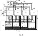
Figure 2 shows an initial configuration of a multiple-chip radar system according to an example embodiment of the invention; -
Figure 3 shows a 'fail functional' configuration of the multiple-chip radar system ofFigure 2 , following detection of a fault in a first IC of the system; and -
Figure 4 is a flow diagram illustrating a method according to an example embodiment of the invention. -
Figure 1 shows an example configuration of a cascaded multiple-chipradar sensor system 100, for example an array sensor, useful for understanding the present invention. Thesystem 100 comprises amaster transceiver 110 in the form of a master integrated circuit (IC), a number ofslave transceivers Figure 1 ), a controller in the form of a main computing unit (MCU) 150, and acrystal oscillator 160. Typically, eachIC - The
crystal oscillator 160 generates a reference clock signal 180 (XTAL1, XTAL2) for themaster IC 110. As an example, thereference clock signal 180 may be a differential signal having a frequency of 60MHz. - The master IC 110 generates a common local oscillator (LO)
signal 200, which is output from anLO output port 200a of the master IC 110. Thecommon LO signal 200 is distributed via power splitters/dividers 200b to respectiveLO input ports 200c of the master IC 110 andslave ICs Figure 1 ) of theICs LO output port 200a to eachLO input port 200c are aligned to avoid phase differences. Thecommon LO signal 200 may have a frequency of, for example, 38GHz. - The master IC 110 also generates a common clock signal 210 (MS_CLKn, MS_CLKp), used as a time base for synchronization of the sampling moments on the ADCs on the master and slave ICs. As an example, the common clock signal may be a differential signal having a frequency of 240 MHz.
- Both the
common LO signal 200 and thecommon clock signal 210 are derived from thereference clock signal 180 received by the master IC 110 from thecrystal oscillator 160. - The master IC 110 also transmits timing control signals (not shown) to the
slave ICs - The
MCU 150 is connected to the master andslave ICs control lines 220 anddigital lines 230, for example using CSI-2 or LVDS formats, for receiving data from the master andslave ICs MCU 150 may comprise digital signal processing (DSP) functionality and may comprise field programmable gate arrays (FPGA). TheMCU 150 is also connected to the master andslave ICs control lines 240 for triggering the start of a data acquisition sequence. - In the event of a failure of the
master IC 110 in theradar system 100, thewhole system 100 will fail since the commonlocal oscillator signal 200 and thecommon clock signal 210 will not be distributed to theslave ICs -
Figure 2 shows an example configuration of a multiple-chipradar sensor system 300 according to an embodiment of the present invention. Thesystem 300 comprises a first integrated circuit (IC) 310 in the form of a first transceiver, and a number offurther ICs Figure 2 ), a controller in the form of a main computing unit (MCU) 350, and acrystal oscillator 360. Typically, eachIC - The
crystal oscillator 360 generates a reference clock signal 380 (XTAL1, XTAL2) which is distributed to each of the first andfurther ICs reference clock signal 380 may be a differential signal having a frequency of 60MHz. - As in the previous example, the
MCU 350 is connected to thetransceivers control lines 420 anddigital lines 430, for example using CSI-2 or LVDS formats, for receiving data from thetransceivers MCU 350 may comprise digital signal processing (DSP) functionality and may comprise field programmable gate arrays (FPGA). TheMCU 350 is also connected to thetransceivers control lines 440 for triggering the start of a data acquisition sequence. - The
radar system 300 differs from thesystem 100 of the previous example in that theMCU 350 is also connected to each of thetransceivers slave control line 450. Thiscontrol line 450 is used for enabling a master mode or a slave mode of operation in each transceiver. The master/slave control line 450 may connect to a GPIO input of therespective transceiver - The
first transceiver 310 is operable as a master IC for thesystem 300. When operating as master IC, thefirst transceiver 310 is configured to generate a common local oscillator (LO) signal 400 and a common clock signal 410 (MS_CLKn, MS_CLKp), each derived from thereference clock signal 380 received by thefirst transceiver 310 from thecrystal oscillator 360. Thecommon LO signal 400 may be output from anLO output port 400a of thefirst transceiver 310 and distributed via power splitters/dividers 400b to respectiveLO input ports 400c of thefirst transceiver 310 andfurther transceivers Figure 2 ) of thetransceivers LO output port 400a to eachLO input port 400c are aligned to avoid phase differences. Thecommon LO signal 400 may have a frequency of, for example, 38GHz. Thecommon clock signal 410 is used as a time base for synchronization of the sampling moments on the ADCs on thetransceivers first transceiver 310 also transmits timing control signals (not shown) to thefurther transceivers - The
further transceivers first transceiver 310 operating as master IC. When operating in the slave mode, thefurther transceivers local oscillator signal 400 received at their respectiveLO input ports 400c from thefirst transceiver 310. When operating in slave mode, thefurther transceivers common clock signal 410 received from thefirst transceiver 310. - However, the
further transceivers further transceivers reference clock signal 380 received directly from thecrystal oscillator 360, instead of using thecommon LO signal 400 received at its respectiveLO input port 400c. Thefurther transceivers reference clock signal 380, instead of using thecommon clock signal 410 received from thefirst transceiver 310. - The
first transceiver 310 andfurther transceivers transceiver transceiver MCU 350 via the master/slave control line 450 during initialisation of thesystem 300. In other embodiments, thefirst transceiver 310 may be permanently configured in master mode, for example by connection of a GPIO input to an address ball. Importantly, thefurther transceivers MCU 350 via the master/slave control line 450 to operate in the master mode following initial configuration in the slave mode. -
Figure 2 illustrates theradar system 300 in an initial configuration, in which thefirst transceiver 310 is configured to operate as a master IC, and thefurther transceivers radar system 300. Theslave ICs common LO signal 400 andcommon clock signal 410 received from themaster IC 310. - The
MCU 350 includes fault detection functionality for detecting a fault in thefirst transceiver 310 orfurther transceivers MCU 350 may be configured to detect a fault in any one of thetransceivers transceiver MCU 350 if the self-test results in a fail. Alternatively, or in addition, theMCU 350 may be programmed to detect some errors directly, for example theMCU 350 may be configured to detect an irregularity in radar data obtained using a particular transceiver, such as an irregularity in an FFT of the radar data, and to interpret such an irregularity as an indication of a fault. - Upon detection by the
MCU 350 of a fault or failure of thefirst transceiver 310 of theradar system 300, during operation in the initial configuration described above with reference toFigure 2 , theMCU 350 sends a signal or signals to asecond transceiver 320, via the master/slave control line 450, thesecond transceiver 320 being one of thefurther transceivers second transceiver 320 from slave mode to master mode. Following reconfiguration to operate in the master mode, thesecond transceiver 320 uses a local, internally-generated LO and a local clock signal, each derived from thereference clock signal 380 received directly from thecrystal oscillator 360. However, the local LO signal generated by thesecond transceiver 320 is not output since there is no provision in the present embodiment for distribution of an LO signal from thesecond transceiver 320 to theother transceivers - Reconfiguration of the
second transceiver 320 may be digitally controlled by theMCU 350, wherein thesecond transceiver 320 automatically implements automatically the reconfiguration process on receipt of a control signal from theMCU 350, via the master/slave control line 450 indicating reconfiguration from the slave mode to the master mode. Alternatively, theMCU 350 may send multiple commands to thesecond transceiver 320 to implement respective multiple steps of the reconfiguration process. For example, the reconfiguration process may require steps such as switching on an internal PLL of thesecond transceiver 320 for generating a local LO signal, switching the LO signal source from theLO input 400c of thesecond transceiver 320 to the local, internally-generated LO signal, and switching the clock signal source from thecommon clock signal 410 to an internally-generated local clock signal. The reconfiguration of thesecond transceiver 320 may be performed by changing the states of various internal switching devices of thesecond transceiver 320. - Following detection of a fault in the first transceiver, the
MCU 350 also disables thefirst transceiver 310, the circuitry for distribution of thecommon LO signal 400, and thefurther transceivers second transceiver 320. As a result, theradar system 300 is reconfigured to the configuration shown inFigure 3 . InFigure 3 , the inactive parts of the system are shown in grey. - In the
radar system 300 reconfigured as shown inFigure 3 , thesecond transceiver 320 operates as a standalone transceiver, thereby enabling theradar system 300 to provide a minimal level of functionality even in the event of a fault in thefirst transceiver 310. This configuration of thesystem 300, shown inFigure 3 , may therefore be referred to as a 'fail functional' configuration. - In other embodiments, the remaining
further transceivers second transceiver 320, to provide an alternative fail functional configuration. However, without any provision for sharing a common LO signal, they each operate in a standalone manner using their respective internally-generated LO signal derived from thereference clock signal 380 from thecrystal oscillator 360. - If the
MCU 350 detects a fault in one of thefurther transceivers radar system 300 in the initial configuration shown inFigure 2 , theMCU 350 disables the faulty transceiver but does not reconfigure any of theother transceivers second transceiver 320 during operation of thesystem 300 in the fail functional configuration shown inFigure 3 , theMCU 350 sends a signal to athird transceiver 330, thethird transceiver 330 being one of thefurther transceivers second transceiver 320, for reconfiguring thethird transceiver 330 from slave mode to master mode, and disables the faultysecond transceiver 320. In this way, thesystem 300 may continue to operate in a further fail functional configuration. - The
radar system 300 shown inFigures 2 and3 includes threefurther transceivers reference clock signal 380 from thecrystal oscillator 360 and each configured for control via the master/slave control line 450 such that theMCU 350 may reconfigure any of thefurther transceivers MCU 350 may select any one of thefurther transceivers first transceiver 310. In other embodiments of the invention, the radar system may include any number, equal to or greater than one, of suchfurther transceivers reference clock signal 380. In other embodiments, all the slave transceivers of the radar system may be configured for reconfiguration between slave and master modes. - The
radar system 300 described above includes ICs in the form ofintegrated transceivers -
Figure 4 illustrates a method of operation of theradar system 300 shown inFigures 2 and3 . - In a
first step 500, theMCU 350 sends a signal via the master/control line 450 to initialise thesystem 300 for normal operation by configuring thefirst transceiver 310 in master mode and thefurther transceivers - In a
next step 510, theradar system 300 operates normally in the initial configuration. Theradar system 300 operates as a cascasded system with thefirst transceiver 310 as master and thefurther transceivers further transceivers common LO signal 400 andcommon clock signal 410 received from thefirst transceiver 310. - In a
next step 520, theMCU 350 monitors for faults in thefirst transceiver 310. If no fault is detected, the method returns to step 510. If a fault is detected, for example by receiving an error signal from thefirst transceiver 310, the method proceeds to step 530. - At
step 530, theMCU 350 disables thefirst transceiver 310. This step may be optional, for example if thefirst transceiver 310 automatically deactivates on detection of an internal fault. - In a
next step 540, theMCU 350 sends a signal to thesecond transceiver 320 instructing reconfiguration of thesecond transceiver 320 from slave mode to master mode. On receipt of this signal, thesecond transceiver 320 automatically reconfigures such that it uses an internally-generated local LO signal derived from thereference clock signal 380 received directly from thecrystal oscillator 360. - In a
next step 550, theMCU 350 disables the otherfurther transceivers 330, 340 (not including the second transceiver 320). This step is optional. - In a
next step 560, theradar system 300 operates in a fail functional configuration. Thesecond transceiver 320 uses an internally-generated local LO signal derived from thereference clock signal 380. - In a
next step 570, theMCU 350 monitors for faults in thesecond transceiver 320. If no fault is detected, the method returns to step 560. If a fault is detected, for example by receiving an error signal from thesecond transceiver 320, the method proceeds to step 580. - At
step 580, theMCU 350 disables thesecond transceiver 320. This step may be optional, for example if thesecond transceiver 320 automatically deactivates on detection of an internal fault. - In a
next step 590, theMCU 350 sends a signal to thethird transceiver 330 instructing reconfiguration of thethird transceiver 330 from slave mode to master mode and/or to enable thethird transceiver 330. On receipt of this signal, thethird transceiver 330 automatically reconfigures such that it uses an internally-generated local LO signal derived from thereference clock signal 380 received directly from thecrystal oscillator 360. - In a
next step 600, theradar system 300 operates in a further fail functional configuration. Thethird transceiver 330 uses an internally-generated LO signal derived from thereference clock signal 380. - Although particular embodiments of the invention have been described above, it will be appreciated than many modifications, including additions and/or substitutions, may be made within the scope of the appended claims.
Claims (15)
- A radar system comprising:a first IC, arranged to receive a reference clock signal and configurable to generate a common local oscillator signal based on said reference clock signal;a second IC, arranged to receive the common local oscillator signal from the first IC; anda controller, adapted to detect a fault in said first IC, and configured, upon detection of a fault in said first IC, to send at least one signal to said second IC for reconfiguring said second IC from a slave mode to a master mode;wherein, when operating in said slave mode, said second IC is configured to use the common local oscillator signal generated by the first IC, and, when operating in said master mode, said second IC is configured to use an internally-generated local oscillator signal.
- A radar system according to claim 1, wherein said second IC is configured to receive said reference clock signal, wherein said internally-generated local oscillator signal is based on said reference clock signal.
- A radar system according to claim 1 or claim 2, wherein said reference clock signal is derived from a crystal oscillator.
- A radar system according to any one of the preceding claims, wherein said controller is configured, upon detection of a fault in said first IC, to disable said first IC.
- A radar system according to any of the preceding claims, comprising a plurality of further ICs, each arranged to receive the common local oscillator signal from the first IC, wherein said second IC is a selected one of said plurality of further ICs.
- A radar system according to claim 5, wherein each said further IC is arranged to receive said reference clock signal.
- A radar system according to claim 5 or claim 6, wherein said controller is configured, upon detection of a fault in said first IC, to disable each of said further ICs other than said second IC.
- A radar system according to any of claims 5 to 7, wherein said controller is adapted to detect a fault in said second IC, and is configured, upon detection of a fault in said second IC, to send at least one signal to a different selected one of said plurality of further ICs for reconfiguring said different selected one of said plurality of further ICs from said slave mode to said master mode.
- A radar system according to any of the preceding claims, wherein said controller is adapted to detect a fault in said first IC by receiving an error signal from said first IC.
- A radar system according to any of the preceding claims, wherein said controller is adapted to detect a fault in said first IC by detecting an irregularity in radar data obtained using said first IC.
- A radar system according to any of the preceding claims, wherein each of said first IC and said second IC is a transceiver IC or is comprised in a transceiver, transmitter, or receiver chipset.
- A radar system according to any of the preceding claims, wherein said first IC is configurable to generate a common clock signal based on said reference clock signal, wherein said second IC is adapted, when operating in said slave mode, to use said common clock signal generated by said first IC.
- A reconfigurable integrated circuit, selectively configurable for use as said first IC or said second IC in a radar system according to any of the preceding claims.
- A method of operating a radar system, the radar system comprising: a first IC arranged to receive a reference clock signal and configurable to generate a common local oscillator signal based on said reference clock signal, a second IC arranged to receive the common local oscillator signal from the first IC, the second IC being selectively configurable for operation in a slave mode, in which said second IC is configured to use the common local oscillator signal output by the first IC, and for operation in a master mode, in which said second IC is configured to use an internally-generated local oscillator signal; the method comprising:detecting a fault in said first IC, andon detection of said fault in said first IC, sending at least one signal to said second IC for reconfiguring said second IC from said slave mode to said master mode.
- A control system for an autonomous vehicle, the control system comprising a radar system according to any one of claims 1 to 12.
Priority Applications (3)
| Application Number | Priority Date | Filing Date | Title |
|---|---|---|---|
| EP18150105.7A EP3505952B1 (en) | 2018-01-02 | 2018-01-02 | Radar apparatus and method |
| US16/221,822 US11132001B2 (en) | 2018-01-02 | 2018-12-17 | Radar apparatus and method |
| CN201910001405.XA CN109991604B (en) | 2018-01-02 | 2019-01-02 | Radar apparatus and method |
Applications Claiming Priority (1)
| Application Number | Priority Date | Filing Date | Title |
|---|---|---|---|
| EP18150105.7A EP3505952B1 (en) | 2018-01-02 | 2018-01-02 | Radar apparatus and method |
Publications (2)
| Publication Number | Publication Date |
|---|---|
| EP3505952A1 true EP3505952A1 (en) | 2019-07-03 |
| EP3505952B1 EP3505952B1 (en) | 2022-04-20 |
Family
ID=60888348
Family Applications (1)
| Application Number | Title | Priority Date | Filing Date |
|---|---|---|---|
| EP18150105.7A Active EP3505952B1 (en) | 2018-01-02 | 2018-01-02 | Radar apparatus and method |
Country Status (3)
| Country | Link |
|---|---|
| US (1) | US11132001B2 (en) |
| EP (1) | EP3505952B1 (en) |
| CN (1) | CN109991604B (en) |
Cited By (2)
| Publication number | Priority date | Publication date | Assignee | Title |
|---|---|---|---|---|
| CN114325715A (en) * | 2022-03-11 | 2022-04-12 | 南京隼眼电子科技有限公司 | Radar structure and system |
| US20240264273A1 (en) * | 2021-08-25 | 2024-08-08 | Hitachi Kokusai Electric Inc. | Radar system, radar device, and monitoring method |
Families Citing this family (12)
| Publication number | Priority date | Publication date | Assignee | Title |
|---|---|---|---|---|
| US9352447B2 (en) | 2009-09-08 | 2016-05-31 | Us Synthetic Corporation | Superabrasive elements and methods for processing and manufacturing the same using protective layers |
| DE102018203464A1 (en) * | 2018-03-08 | 2019-09-12 | Robert Bosch Gmbh | Radar sensor system and method for operating a radar sensor system |
| DE102019106030A1 (en) * | 2018-03-22 | 2019-09-26 | Infineon Technologies Ag | RADAR SYSTEM WITH MULTIPLE RADAR CHIPS |
| US20190377064A1 (en) * | 2018-06-06 | 2019-12-12 | GM Global Technology Operations LLC | Method and apparatus for deicing of sensor systems in a vehicle |
| DE102020107804A1 (en) * | 2019-04-26 | 2020-10-29 | Infineon Technologies Ag | Radar apparatus and method for detecting radar targets |
| CN110501703A (en) * | 2019-08-28 | 2019-11-26 | 南京德睿智芯电子科技有限公司 | A small imaging radar radio frequency transceiver module |
| EP4019998A1 (en) * | 2020-12-23 | 2022-06-29 | NXP USA, Inc. | Distributed radar system |
| CN113055000B (en) * | 2021-03-23 | 2023-08-11 | 加特兰微电子科技(上海)有限公司 | Sensing system, related device and method for acquiring working clock signal |
| US12500731B2 (en) | 2021-03-23 | 2025-12-16 | Calterah Semiconductor Technology (Shanghai) Co., Ltd. | Sensing system, method for obtaining working clock signal, integrated circuit, radio device, and device |
| DE102021107618A1 (en) * | 2021-03-25 | 2022-09-29 | Infineon Technologies Ag | CASCADED HF SYSTEM |
| EP4336218A1 (en) * | 2022-09-07 | 2024-03-13 | Nxp B.V. | Cascaded radar system with improved availability |
| CN116775559B (en) * | 2023-08-17 | 2023-12-01 | 南京楚航科技有限公司 | AWR2X chip data acquisition method, system and device |
Citations (3)
| Publication number | Priority date | Publication date | Assignee | Title |
|---|---|---|---|---|
| US20070014269A1 (en) * | 2005-07-13 | 2007-01-18 | Texas Instruments Incorporated | Apparatus for and method of synchronization and beaconing in a wlan mesh network |
| US20120063296A1 (en) * | 2010-09-10 | 2012-03-15 | Broadcom Corporation | Systems and Methods for Providing a Dual-Master Mode in a Synchronous Ethernet Environment |
| EP2881752A1 (en) * | 2013-12-03 | 2015-06-10 | Nxp B.V. | A multichip automotive radar system, a radar chip for such as system, and a method of operating such a system |
Family Cites Families (9)
| Publication number | Priority date | Publication date | Assignee | Title |
|---|---|---|---|---|
| JP3639056B2 (en) * | 1996-08-16 | 2005-04-13 | 富士通株式会社 | Radar device failure determination device |
| US7089462B2 (en) * | 2003-04-17 | 2006-08-08 | International Business Machines Corporation | Early clock fault detection method and circuit for detecting clock faults in a multiprocessing system |
| US8922421B2 (en) * | 2009-12-10 | 2014-12-30 | Lockheed Martin Corporation | Method and system for use of GPS disciplined oscillators for coherent timing reference in distributed radar systems |
| US9279883B2 (en) * | 2013-02-19 | 2016-03-08 | Infineon Technologies Ag | Method and device for radar applications |
| US9880261B2 (en) * | 2014-09-30 | 2018-01-30 | Texas Instruments Incorporated | Loopback techniques for synchronization of oscillator signal in radar |
| US9910133B2 (en) * | 2015-02-25 | 2018-03-06 | Infineon Technologies Ag | Systems and methods for cascading radar chips having a low leakage buffer |
| CN106526582B (en) * | 2015-08-28 | 2022-10-04 | 安波福技术有限公司 | Bistatic Radar System |
| US10061015B2 (en) * | 2015-09-30 | 2018-08-28 | Texas Instruments Incorporated | Multi-chip transceiver testing in a radar system |
| CN118914992A (en) * | 2018-06-07 | 2024-11-08 | 三菱电机株式会社 | Radar device, fault detection method for radar device, and operation method for radar device |
-
2018
- 2018-01-02 EP EP18150105.7A patent/EP3505952B1/en active Active
- 2018-12-17 US US16/221,822 patent/US11132001B2/en active Active
-
2019
- 2019-01-02 CN CN201910001405.XA patent/CN109991604B/en active Active
Patent Citations (3)
| Publication number | Priority date | Publication date | Assignee | Title |
|---|---|---|---|---|
| US20070014269A1 (en) * | 2005-07-13 | 2007-01-18 | Texas Instruments Incorporated | Apparatus for and method of synchronization and beaconing in a wlan mesh network |
| US20120063296A1 (en) * | 2010-09-10 | 2012-03-15 | Broadcom Corporation | Systems and Methods for Providing a Dual-Master Mode in a Synchronous Ethernet Environment |
| EP2881752A1 (en) * | 2013-12-03 | 2015-06-10 | Nxp B.V. | A multichip automotive radar system, a radar chip for such as system, and a method of operating such a system |
Cited By (3)
| Publication number | Priority date | Publication date | Assignee | Title |
|---|---|---|---|---|
| US20240264273A1 (en) * | 2021-08-25 | 2024-08-08 | Hitachi Kokusai Electric Inc. | Radar system, radar device, and monitoring method |
| US12282113B2 (en) * | 2021-08-25 | 2025-04-22 | Kokusai Denki Electric Inc. | Radar system, radar device, and monitoring method |
| CN114325715A (en) * | 2022-03-11 | 2022-04-12 | 南京隼眼电子科技有限公司 | Radar structure and system |
Also Published As
| Publication number | Publication date |
|---|---|
| EP3505952B1 (en) | 2022-04-20 |
| CN109991604A (en) | 2019-07-09 |
| US20190204846A1 (en) | 2019-07-04 |
| US11132001B2 (en) | 2021-09-28 |
| CN109991604B (en) | 2024-06-18 |
Similar Documents
| Publication | Publication Date | Title |
|---|---|---|
| EP3505952B1 (en) | Radar apparatus and method | |
| US11262436B2 (en) | Multi-chip transceiver testing in a radar system | |
| US11320488B2 (en) | Self test for safety logic | |
| US10591585B2 (en) | Electronic control unit for radar sensors | |
| US10038508B1 (en) | Wireless communication unit diagnostics | |
| US8924772B2 (en) | Fault-tolerant system and fault-tolerant control method | |
| CN107953890B (en) | Method for processing data for an automated vehicle | |
| CN110297217A (en) | Radar system with multiple radar chips | |
| US20090106606A1 (en) | Method and apparatus for detecting and isolating controller area network permanent dominant states | |
| US11436180B2 (en) | I3C slave interface, integrated circuit including an I3C slave interface, and method for operating an I3C slave interface | |
| US5357491A (en) | Clock selection control device | |
| CN111694304B (en) | Comprehensive fault logic decision circuit and method for spacecraft | |
| US20240077578A1 (en) | Cascaded radar system with improved availability | |
| JPH0362213A (en) | Information transfer system | |
| US11946972B2 (en) | Monitoring of interconnect lines | |
| US7167410B2 (en) | Memory system and memory device having a serial interface | |
| US8335277B2 (en) | Method and apparatus for checking asynchronous transmission of control signals | |
| JP7164483B2 (en) | Electronic controller, control system | |
| CN120803993A (en) | Transmission management device, integrated circuit and controller | |
| KR20200008247A (en) | Atmospheric Plasma Device | |
| JP2016219959A (en) | Electronic control unit | |
| JPS62274292A (en) | Digital time unit |
Legal Events
| Date | Code | Title | Description |
|---|---|---|---|
| PUAI | Public reference made under article 153(3) epc to a published international application that has entered the european phase |
Free format text: ORIGINAL CODE: 0009012 |
|
| STAA | Information on the status of an ep patent application or granted ep patent |
Free format text: STATUS: THE APPLICATION HAS BEEN PUBLISHED |
|
| AK | Designated contracting states |
Kind code of ref document: A1 Designated state(s): AL AT BE BG CH CY CZ DE DK EE ES FI FR GB GR HR HU IE IS IT LI LT LU LV MC MK MT NL NO PL PT RO RS SE SI SK SM TR |
|
| AX | Request for extension of the european patent |
Extension state: BA ME |
|
| STAA | Information on the status of an ep patent application or granted ep patent |
Free format text: STATUS: REQUEST FOR EXAMINATION WAS MADE |
|
| 17P | Request for examination filed |
Effective date: 20200103 |
|
| RBV | Designated contracting states (corrected) |
Designated state(s): AL AT BE BG CH CY CZ DE DK EE ES FI FR GB GR HR HU IE IS IT LI LT LU LV MC MK MT NL NO PL PT RO RS SE SI SK SM TR |
|
| REG | Reference to a national code |
Ref country code: DE Ref legal event code: R079 Ref document number: 602018033994 Country of ref document: DE Free format text: PREVIOUS MAIN CLASS: G01S0007400000 Ipc: G01S0013931000 |
|
| RIC1 | Information provided on ipc code assigned before grant |
Ipc: G01S 7/03 20060101ALI20211123BHEP Ipc: G01S 7/40 20060101ALI20211123BHEP Ipc: G01S 13/931 20200101AFI20211123BHEP |
|
| GRAP | Despatch of communication of intention to grant a patent |
Free format text: ORIGINAL CODE: EPIDOSNIGR1 |
|
| STAA | Information on the status of an ep patent application or granted ep patent |
Free format text: STATUS: GRANT OF PATENT IS INTENDED |
|
| INTG | Intention to grant announced |
Effective date: 20220110 |
|
| GRAS | Grant fee paid |
Free format text: ORIGINAL CODE: EPIDOSNIGR3 |
|
| GRAA | (expected) grant |
Free format text: ORIGINAL CODE: 0009210 |
|
| STAA | Information on the status of an ep patent application or granted ep patent |
Free format text: STATUS: THE PATENT HAS BEEN GRANTED |
|
| AK | Designated contracting states |
Kind code of ref document: B1 Designated state(s): AL AT BE BG CH CY CZ DE DK EE ES FI FR GB GR HR HU IE IS IT LI LT LU LV MC MK MT NL NO PL PT RO RS SE SI SK SM TR |
|
| REG | Reference to a national code |
Ref country code: GB Ref legal event code: FG4D |
|
| REG | Reference to a national code |
Ref country code: CH Ref legal event code: EP |
|
| REG | Reference to a national code |
Ref country code: IE Ref legal event code: FG4D |
|
| REG | Reference to a national code |
Ref country code: DE Ref legal event code: R096 Ref document number: 602018033994 Country of ref document: DE |
|
| REG | Reference to a national code |
Ref country code: AT Ref legal event code: REF Ref document number: 1485579 Country of ref document: AT Kind code of ref document: T Effective date: 20220515 |
|
| REG | Reference to a national code |
Ref country code: LT Ref legal event code: MG9D |
|
| REG | Reference to a national code |
Ref country code: NL Ref legal event code: MP Effective date: 20220420 |
|
| REG | Reference to a national code |
Ref country code: AT Ref legal event code: MK05 Ref document number: 1485579 Country of ref document: AT Kind code of ref document: T Effective date: 20220420 |
|
| PG25 | Lapsed in a contracting state [announced via postgrant information from national office to epo] |
Ref country code: NL Free format text: LAPSE BECAUSE OF FAILURE TO SUBMIT A TRANSLATION OF THE DESCRIPTION OR TO PAY THE FEE WITHIN THE PRESCRIBED TIME-LIMIT Effective date: 20220420 |
|
| PG25 | Lapsed in a contracting state [announced via postgrant information from national office to epo] |
Ref country code: SE Free format text: LAPSE BECAUSE OF FAILURE TO SUBMIT A TRANSLATION OF THE DESCRIPTION OR TO PAY THE FEE WITHIN THE PRESCRIBED TIME-LIMIT Effective date: 20220420 Ref country code: PT Free format text: LAPSE BECAUSE OF FAILURE TO SUBMIT A TRANSLATION OF THE DESCRIPTION OR TO PAY THE FEE WITHIN THE PRESCRIBED TIME-LIMIT Effective date: 20220822 Ref country code: NO Free format text: LAPSE BECAUSE OF FAILURE TO SUBMIT A TRANSLATION OF THE DESCRIPTION OR TO PAY THE FEE WITHIN THE PRESCRIBED TIME-LIMIT Effective date: 20220720 Ref country code: LT Free format text: LAPSE BECAUSE OF FAILURE TO SUBMIT A TRANSLATION OF THE DESCRIPTION OR TO PAY THE FEE WITHIN THE PRESCRIBED TIME-LIMIT Effective date: 20220420 Ref country code: HR Free format text: LAPSE BECAUSE OF FAILURE TO SUBMIT A TRANSLATION OF THE DESCRIPTION OR TO PAY THE FEE WITHIN THE PRESCRIBED TIME-LIMIT Effective date: 20220420 Ref country code: GR Free format text: LAPSE BECAUSE OF FAILURE TO SUBMIT A TRANSLATION OF THE DESCRIPTION OR TO PAY THE FEE WITHIN THE PRESCRIBED TIME-LIMIT Effective date: 20220721 Ref country code: FI Free format text: LAPSE BECAUSE OF FAILURE TO SUBMIT A TRANSLATION OF THE DESCRIPTION OR TO PAY THE FEE WITHIN THE PRESCRIBED TIME-LIMIT Effective date: 20220420 Ref country code: ES Free format text: LAPSE BECAUSE OF FAILURE TO SUBMIT A TRANSLATION OF THE DESCRIPTION OR TO PAY THE FEE WITHIN THE PRESCRIBED TIME-LIMIT Effective date: 20220420 Ref country code: BG Free format text: LAPSE BECAUSE OF FAILURE TO SUBMIT A TRANSLATION OF THE DESCRIPTION OR TO PAY THE FEE WITHIN THE PRESCRIBED TIME-LIMIT Effective date: 20220720 Ref country code: AT Free format text: LAPSE BECAUSE OF FAILURE TO SUBMIT A TRANSLATION OF THE DESCRIPTION OR TO PAY THE FEE WITHIN THE PRESCRIBED TIME-LIMIT Effective date: 20220420 |
|
| PG25 | Lapsed in a contracting state [announced via postgrant information from national office to epo] |
Ref country code: RS Free format text: LAPSE BECAUSE OF FAILURE TO SUBMIT A TRANSLATION OF THE DESCRIPTION OR TO PAY THE FEE WITHIN THE PRESCRIBED TIME-LIMIT Effective date: 20220420 Ref country code: PL Free format text: LAPSE BECAUSE OF FAILURE TO SUBMIT A TRANSLATION OF THE DESCRIPTION OR TO PAY THE FEE WITHIN THE PRESCRIBED TIME-LIMIT Effective date: 20220420 Ref country code: LV Free format text: LAPSE BECAUSE OF FAILURE TO SUBMIT A TRANSLATION OF THE DESCRIPTION OR TO PAY THE FEE WITHIN THE PRESCRIBED TIME-LIMIT Effective date: 20220420 Ref country code: IS Free format text: LAPSE BECAUSE OF FAILURE TO SUBMIT A TRANSLATION OF THE DESCRIPTION OR TO PAY THE FEE WITHIN THE PRESCRIBED TIME-LIMIT Effective date: 20220820 |
|
| REG | Reference to a national code |
Ref country code: DE Ref legal event code: R097 Ref document number: 602018033994 Country of ref document: DE |
|
| PG25 | Lapsed in a contracting state [announced via postgrant information from national office to epo] |
Ref country code: SM Free format text: LAPSE BECAUSE OF FAILURE TO SUBMIT A TRANSLATION OF THE DESCRIPTION OR TO PAY THE FEE WITHIN THE PRESCRIBED TIME-LIMIT Effective date: 20220420 Ref country code: SK Free format text: LAPSE BECAUSE OF FAILURE TO SUBMIT A TRANSLATION OF THE DESCRIPTION OR TO PAY THE FEE WITHIN THE PRESCRIBED TIME-LIMIT Effective date: 20220420 Ref country code: RO Free format text: LAPSE BECAUSE OF FAILURE TO SUBMIT A TRANSLATION OF THE DESCRIPTION OR TO PAY THE FEE WITHIN THE PRESCRIBED TIME-LIMIT Effective date: 20220420 Ref country code: EE Free format text: LAPSE BECAUSE OF FAILURE TO SUBMIT A TRANSLATION OF THE DESCRIPTION OR TO PAY THE FEE WITHIN THE PRESCRIBED TIME-LIMIT Effective date: 20220420 Ref country code: DK Free format text: LAPSE BECAUSE OF FAILURE TO SUBMIT A TRANSLATION OF THE DESCRIPTION OR TO PAY THE FEE WITHIN THE PRESCRIBED TIME-LIMIT Effective date: 20220420 Ref country code: CZ Free format text: LAPSE BECAUSE OF FAILURE TO SUBMIT A TRANSLATION OF THE DESCRIPTION OR TO PAY THE FEE WITHIN THE PRESCRIBED TIME-LIMIT Effective date: 20220420 |
|
| PLBE | No opposition filed within time limit |
Free format text: ORIGINAL CODE: 0009261 |
|
| STAA | Information on the status of an ep patent application or granted ep patent |
Free format text: STATUS: NO OPPOSITION FILED WITHIN TIME LIMIT |
|
| 26N | No opposition filed |
Effective date: 20230123 |
|
| PG25 | Lapsed in a contracting state [announced via postgrant information from national office to epo] |
Ref country code: AL Free format text: LAPSE BECAUSE OF FAILURE TO SUBMIT A TRANSLATION OF THE DESCRIPTION OR TO PAY THE FEE WITHIN THE PRESCRIBED TIME-LIMIT Effective date: 20220420 |
|
| PG25 | Lapsed in a contracting state [announced via postgrant information from national office to epo] |
Ref country code: SI Free format text: LAPSE BECAUSE OF FAILURE TO SUBMIT A TRANSLATION OF THE DESCRIPTION OR TO PAY THE FEE WITHIN THE PRESCRIBED TIME-LIMIT Effective date: 20220420 |
|
| P01 | Opt-out of the competence of the unified patent court (upc) registered |
Effective date: 20230725 |
|
| REG | Reference to a national code |
Ref country code: CH Ref legal event code: PL |
|
| GBPC | Gb: european patent ceased through non-payment of renewal fee |
Effective date: 20230102 |
|
| PG25 | Lapsed in a contracting state [announced via postgrant information from national office to epo] |
Ref country code: LU Free format text: LAPSE BECAUSE OF NON-PAYMENT OF DUE FEES Effective date: 20230102 |
|
| REG | Reference to a national code |
Ref country code: BE Ref legal event code: MM Effective date: 20230131 |
|
| PG25 | Lapsed in a contracting state [announced via postgrant information from national office to epo] |
Ref country code: LI Free format text: LAPSE BECAUSE OF NON-PAYMENT OF DUE FEES Effective date: 20230131 Ref country code: GB Free format text: LAPSE BECAUSE OF NON-PAYMENT OF DUE FEES Effective date: 20230102 Ref country code: CH Free format text: LAPSE BECAUSE OF NON-PAYMENT OF DUE FEES Effective date: 20230131 |
|
| PG25 | Lapsed in a contracting state [announced via postgrant information from national office to epo] |
Ref country code: BE Free format text: LAPSE BECAUSE OF NON-PAYMENT OF DUE FEES Effective date: 20230131 |
|
| PG25 | Lapsed in a contracting state [announced via postgrant information from national office to epo] |
Ref country code: IT Free format text: LAPSE BECAUSE OF FAILURE TO SUBMIT A TRANSLATION OF THE DESCRIPTION OR TO PAY THE FEE WITHIN THE PRESCRIBED TIME-LIMIT Effective date: 20220420 Ref country code: IE Free format text: LAPSE BECAUSE OF NON-PAYMENT OF DUE FEES Effective date: 20230102 |
|
| PG25 | Lapsed in a contracting state [announced via postgrant information from national office to epo] |
Ref country code: MC Free format text: LAPSE BECAUSE OF FAILURE TO SUBMIT A TRANSLATION OF THE DESCRIPTION OR TO PAY THE FEE WITHIN THE PRESCRIBED TIME-LIMIT Effective date: 20220420 |
|
| PG25 | Lapsed in a contracting state [announced via postgrant information from national office to epo] |
Ref country code: MC Free format text: LAPSE BECAUSE OF FAILURE TO SUBMIT A TRANSLATION OF THE DESCRIPTION OR TO PAY THE FEE WITHIN THE PRESCRIBED TIME-LIMIT Effective date: 20220420 |
|
| PG25 | Lapsed in a contracting state [announced via postgrant information from national office to epo] |
Ref country code: BG Free format text: LAPSE BECAUSE OF FAILURE TO SUBMIT A TRANSLATION OF THE DESCRIPTION OR TO PAY THE FEE WITHIN THE PRESCRIBED TIME-LIMIT Effective date: 20220420 |
|
| PG25 | Lapsed in a contracting state [announced via postgrant information from national office to epo] |
Ref country code: BG Free format text: LAPSE BECAUSE OF FAILURE TO SUBMIT A TRANSLATION OF THE DESCRIPTION OR TO PAY THE FEE WITHIN THE PRESCRIBED TIME-LIMIT Effective date: 20220420 |
|
| PG25 | Lapsed in a contracting state [announced via postgrant information from national office to epo] |
Ref country code: CY Free format text: LAPSE BECAUSE OF FAILURE TO SUBMIT A TRANSLATION OF THE DESCRIPTION OR TO PAY THE FEE WITHIN THE PRESCRIBED TIME-LIMIT; INVALID AB INITIO Effective date: 20180102 |
|
| PG25 | Lapsed in a contracting state [announced via postgrant information from national office to epo] |
Ref country code: HU Free format text: LAPSE BECAUSE OF FAILURE TO SUBMIT A TRANSLATION OF THE DESCRIPTION OR TO PAY THE FEE WITHIN THE PRESCRIBED TIME-LIMIT; INVALID AB INITIO Effective date: 20180102 |
|
| PG25 | Lapsed in a contracting state [announced via postgrant information from national office to epo] |
Ref country code: TR Free format text: LAPSE BECAUSE OF FAILURE TO SUBMIT A TRANSLATION OF THE DESCRIPTION OR TO PAY THE FEE WITHIN THE PRESCRIBED TIME-LIMIT Effective date: 20220420 |
|
| PGFP | Annual fee paid to national office [announced via postgrant information from national office to epo] |
Ref country code: FR Payment date: 20251217 Year of fee payment: 9 |
|
| PGFP | Annual fee paid to national office [announced via postgrant information from national office to epo] |
Ref country code: DE Payment date: 20251217 Year of fee payment: 9 |