EP3505490A1 - A method for forming a qubit device - Google Patents
A method for forming a qubit device Download PDFInfo
- Publication number
- EP3505490A1 EP3505490A1 EP17211120.5A EP17211120A EP3505490A1 EP 3505490 A1 EP3505490 A1 EP 3505490A1 EP 17211120 A EP17211120 A EP 17211120A EP 3505490 A1 EP3505490 A1 EP 3505490A1
- Authority
- EP
- European Patent Office
- Prior art keywords
- gate electrode
- substrate
- insulating layer
- forming
- contact
- Prior art date
- Legal status (The legal status is an assumption and is not a legal conclusion. Google has not performed a legal analysis and makes no representation as to the accuracy of the status listed.)
- Granted
Links
Images







Classifications
-
- B—PERFORMING OPERATIONS; TRANSPORTING
- B82—NANOTECHNOLOGY
- B82Y—SPECIFIC USES OR APPLICATIONS OF NANOSTRUCTURES; MEASUREMENT OR ANALYSIS OF NANOSTRUCTURES; MANUFACTURE OR TREATMENT OF NANOSTRUCTURES
- B82Y10/00—Nanotechnology for information processing, storage or transmission, e.g. quantum computing or single electron logic
-
- H—ELECTRICITY
- H10—SEMICONDUCTOR DEVICES; ELECTRIC SOLID-STATE DEVICES NOT OTHERWISE PROVIDED FOR
- H10D—INORGANIC ELECTRIC SEMICONDUCTOR DEVICES
- H10D64/00—Electrodes of devices having potential barriers
- H10D64/60—Electrodes characterised by their materials
- H10D64/608—Electrodes characterised by their materials being superconducting
-
- H—ELECTRICITY
- H10—SEMICONDUCTOR DEVICES; ELECTRIC SOLID-STATE DEVICES NOT OTHERWISE PROVIDED FOR
- H10D—INORGANIC ELECTRIC SEMICONDUCTOR DEVICES
- H10D30/00—Field-effect transistors [FET]
- H10D30/01—Manufacture or treatment
- H10D30/021—Manufacture or treatment of FETs having insulated gates [IGFET]
-
- H—ELECTRICITY
- H10—SEMICONDUCTOR DEVICES; ELECTRIC SOLID-STATE DEVICES NOT OTHERWISE PROVIDED FOR
- H10D—INORGANIC ELECTRIC SEMICONDUCTOR DEVICES
- H10D30/00—Field-effect transistors [FET]
- H10D30/01—Manufacture or treatment
- H10D30/021—Manufacture or treatment of FETs having insulated gates [IGFET]
- H10D30/031—Manufacture or treatment of FETs having insulated gates [IGFET] of thin-film transistors [TFT]
-
- H—ELECTRICITY
- H10—SEMICONDUCTOR DEVICES; ELECTRIC SOLID-STATE DEVICES NOT OTHERWISE PROVIDED FOR
- H10D—INORGANIC ELECTRIC SEMICONDUCTOR DEVICES
- H10D30/00—Field-effect transistors [FET]
- H10D30/40—FETs having zero-dimensional [0D], one-dimensional [1D] or two-dimensional [2D] charge carrier gas channels
- H10D30/402—Single electron transistors; Coulomb blockade transistors
-
- H—ELECTRICITY
- H10—SEMICONDUCTOR DEVICES; ELECTRIC SOLID-STATE DEVICES NOT OTHERWISE PROVIDED FOR
- H10D—INORGANIC ELECTRIC SEMICONDUCTOR DEVICES
- H10D30/00—Field-effect transistors [FET]
- H10D30/60—Insulated-gate field-effect transistors [IGFET]
- H10D30/67—Thin-film transistors [TFT]
- H10D30/6729—Thin-film transistors [TFT] characterised by the electrodes
-
- H—ELECTRICITY
- H10—SEMICONDUCTOR DEVICES; ELECTRIC SOLID-STATE DEVICES NOT OTHERWISE PROVIDED FOR
- H10D—INORGANIC ELECTRIC SEMICONDUCTOR DEVICES
- H10D30/00—Field-effect transistors [FET]
- H10D30/60—Insulated-gate field-effect transistors [IGFET]
- H10D30/67—Thin-film transistors [TFT]
- H10D30/6729—Thin-film transistors [TFT] characterised by the electrodes
- H10D30/673—Thin-film transistors [TFT] characterised by the electrodes characterised by the shapes, relative sizes or dispositions of the gate electrodes
-
- H—ELECTRICITY
- H10—SEMICONDUCTOR DEVICES; ELECTRIC SOLID-STATE DEVICES NOT OTHERWISE PROVIDED FOR
- H10D—INORGANIC ELECTRIC SEMICONDUCTOR DEVICES
- H10D30/00—Field-effect transistors [FET]
- H10D30/60—Insulated-gate field-effect transistors [IGFET]
- H10D30/67—Thin-film transistors [TFT]
- H10D30/674—Thin-film transistors [TFT] characterised by the active materials
- H10D30/675—Group III-V materials, Group II-VI materials, Group IV-VI materials, selenium or tellurium
-
- H—ELECTRICITY
- H10—SEMICONDUCTOR DEVICES; ELECTRIC SOLID-STATE DEVICES NOT OTHERWISE PROVIDED FOR
- H10D—INORGANIC ELECTRIC SEMICONDUCTOR DEVICES
- H10D30/00—Field-effect transistors [FET]
- H10D30/60—Insulated-gate field-effect transistors [IGFET]
- H10D30/67—Thin-film transistors [TFT]
- H10D30/6757—Thin-film transistors [TFT] characterised by the structure of the channel, e.g. transverse or longitudinal shape or doping profile
-
- H—ELECTRICITY
- H10—SEMICONDUCTOR DEVICES; ELECTRIC SOLID-STATE DEVICES NOT OTHERWISE PROVIDED FOR
- H10D—INORGANIC ELECTRIC SEMICONDUCTOR DEVICES
- H10D48/00—Individual devices not covered by groups H10D1/00 - H10D44/00
- H10D48/383—Quantum effect devices, e.g. of devices using quantum reflection, diffraction or interference effects
-
- H—ELECTRICITY
- H10—SEMICONDUCTOR DEVICES; ELECTRIC SOLID-STATE DEVICES NOT OTHERWISE PROVIDED FOR
- H10D—INORGANIC ELECTRIC SEMICONDUCTOR DEVICES
- H10D48/00—Individual devices not covered by groups H10D1/00 - H10D44/00
- H10D48/383—Quantum effect devices, e.g. of devices using quantum reflection, diffraction or interference effects
- H10D48/3835—Semiconductor qubit devices comprising a plurality of quantum mechanically interacting semiconductor quantum dots, e.g. Loss-DiVincenzo spin qubits
-
- H—ELECTRICITY
- H10—SEMICONDUCTOR DEVICES; ELECTRIC SOLID-STATE DEVICES NOT OTHERWISE PROVIDED FOR
- H10D—INORGANIC ELECTRIC SEMICONDUCTOR DEVICES
- H10D62/00—Semiconductor bodies, or regions thereof, of devices having potential barriers
- H10D62/10—Shapes, relative sizes or dispositions of the regions of the semiconductor bodies; Shapes of the semiconductor bodies
- H10D62/117—Shapes of semiconductor bodies
- H10D62/118—Nanostructure semiconductor bodies
- H10D62/119—Nanowire, nanosheet or nanotube semiconductor bodies
- H10D62/121—Nanowire, nanosheet or nanotube semiconductor bodies oriented parallel to substrates
-
- H—ELECTRICITY
- H10—SEMICONDUCTOR DEVICES; ELECTRIC SOLID-STATE DEVICES NOT OTHERWISE PROVIDED FOR
- H10D—INORGANIC ELECTRIC SEMICONDUCTOR DEVICES
- H10D62/00—Semiconductor bodies, or regions thereof, of devices having potential barriers
- H10D62/10—Shapes, relative sizes or dispositions of the regions of the semiconductor bodies; Shapes of the semiconductor bodies
- H10D62/13—Semiconductor regions connected to electrodes carrying current to be rectified, amplified or switched, e.g. source or drain regions
- H10D62/149—Source or drain regions of field-effect devices
- H10D62/151—Source or drain regions of field-effect devices of IGFETs
-
- H—ELECTRICITY
- H10—SEMICONDUCTOR DEVICES; ELECTRIC SOLID-STATE DEVICES NOT OTHERWISE PROVIDED FOR
- H10D—INORGANIC ELECTRIC SEMICONDUCTOR DEVICES
- H10D64/00—Electrodes of devices having potential barriers
- H10D64/01—Manufacture or treatment
- H10D64/011—Manufacture or treatment of electrodes ohmically coupled to a semiconductor
- H10D64/0116—Manufacture or treatment of electrodes ohmically coupled to a semiconductor to Group III-V semiconductors
-
- H—ELECTRICITY
- H10—SEMICONDUCTOR DEVICES; ELECTRIC SOLID-STATE DEVICES NOT OTHERWISE PROVIDED FOR
- H10D—INORGANIC ELECTRIC SEMICONDUCTOR DEVICES
- H10D64/00—Electrodes of devices having potential barriers
- H10D64/01—Manufacture or treatment
- H10D64/013—Manufacture or treatment of electrodes having a conductor capacitively coupled to a semiconductor by an insulator
- H10D64/01358—Manufacture or treatment of electrodes having a conductor capacitively coupled to a semiconductor by an insulator the insulator being formed after the semiconductor body, the semiconductor being a Group III-V material
-
- H—ELECTRICITY
- H10—SEMICONDUCTOR DEVICES; ELECTRIC SOLID-STATE DEVICES NOT OTHERWISE PROVIDED FOR
- H10D—INORGANIC ELECTRIC SEMICONDUCTOR DEVICES
- H10D64/00—Electrodes of devices having potential barriers
- H10D64/20—Electrodes characterised by their shapes, relative sizes or dispositions
- H10D64/205—Nanosized electrodes, e.g. nanowire electrodes
-
- H—ELECTRICITY
- H10—SEMICONDUCTOR DEVICES; ELECTRIC SOLID-STATE DEVICES NOT OTHERWISE PROVIDED FOR
- H10D—INORGANIC ELECTRIC SEMICONDUCTOR DEVICES
- H10D64/00—Electrodes of devices having potential barriers
- H10D64/20—Electrodes characterised by their shapes, relative sizes or dispositions
- H10D64/27—Electrodes not carrying the current to be rectified, amplified, oscillated or switched, e.g. gates
- H10D64/311—Gate electrodes for field-effect devices
- H10D64/411—Gate electrodes for field-effect devices for FETs
- H10D64/511—Gate electrodes for field-effect devices for FETs for IGFETs
- H10D64/512—Disposition of the gate electrodes, e.g. buried gates
-
- H—ELECTRICITY
- H10—SEMICONDUCTOR DEVICES; ELECTRIC SOLID-STATE DEVICES NOT OTHERWISE PROVIDED FOR
- H10N—ELECTRIC SOLID-STATE DEVICES NOT OTHERWISE PROVIDED FOR
- H10N60/00—Superconducting devices
- H10N60/10—Junction-based devices
- H10N60/128—Junction-based devices having three or more electrodes, e.g. transistor-like structures
-
- H—ELECTRICITY
- H10—SEMICONDUCTOR DEVICES; ELECTRIC SOLID-STATE DEVICES NOT OTHERWISE PROVIDED FOR
- H10P—GENERIC PROCESSES OR APPARATUS FOR THE MANUFACTURE OR TREATMENT OF DEVICES COVERED BY CLASS H10
- H10P14/00—Formation of materials, e.g. in the shape of layers or pillars
- H10P14/20—Formation of materials, e.g. in the shape of layers or pillars of semiconductor materials
- H10P14/34—Deposited materials, e.g. layers
- H10P14/3402—Deposited materials, e.g. layers characterised by the chemical composition
- H10P14/3414—Deposited materials, e.g. layers characterised by the chemical composition being group IIIA-VIA materials
- H10P14/3421—Arsenides
-
- H—ELECTRICITY
- H10—SEMICONDUCTOR DEVICES; ELECTRIC SOLID-STATE DEVICES NOT OTHERWISE PROVIDED FOR
- H10P—GENERIC PROCESSES OR APPARATUS FOR THE MANUFACTURE OR TREATMENT OF DEVICES COVERED BY CLASS H10
- H10P14/00—Formation of materials, e.g. in the shape of layers or pillars
- H10P14/20—Formation of materials, e.g. in the shape of layers or pillars of semiconductor materials
- H10P14/34—Deposited materials, e.g. layers
- H10P14/3402—Deposited materials, e.g. layers characterised by the chemical composition
- H10P14/3414—Deposited materials, e.g. layers characterised by the chemical composition being group IIIA-VIA materials
- H10P14/3422—Antimonides
-
- H—ELECTRICITY
- H10—SEMICONDUCTOR DEVICES; ELECTRIC SOLID-STATE DEVICES NOT OTHERWISE PROVIDED FOR
- H10P—GENERIC PROCESSES OR APPARATUS FOR THE MANUFACTURE OR TREATMENT OF DEVICES COVERED BY CLASS H10
- H10P14/00—Formation of materials, e.g. in the shape of layers or pillars
- H10P14/20—Formation of materials, e.g. in the shape of layers or pillars of semiconductor materials
- H10P14/34—Deposited materials, e.g. layers
- H10P14/3451—Structure
- H10P14/3452—Microstructure
- H10P14/3462—Nanowires
-
- H—ELECTRICITY
- H10—SEMICONDUCTOR DEVICES; ELECTRIC SOLID-STATE DEVICES NOT OTHERWISE PROVIDED FOR
- H10P—GENERIC PROCESSES OR APPARATUS FOR THE MANUFACTURE OR TREATMENT OF DEVICES COVERED BY CLASS H10
- H10P14/00—Formation of materials, e.g. in the shape of layers or pillars
- H10P14/40—Formation of materials, e.g. in the shape of layers or pillars of conductive or resistive materials
-
- H—ELECTRICITY
- H10—SEMICONDUCTOR DEVICES; ELECTRIC SOLID-STATE DEVICES NOT OTHERWISE PROVIDED FOR
- H10P—GENERIC PROCESSES OR APPARATUS FOR THE MANUFACTURE OR TREATMENT OF DEVICES COVERED BY CLASS H10
- H10P50/00—Etching of wafers, substrates or parts of devices
- H10P50/60—Wet etching
- H10P50/64—Wet etching of semiconductor materials
- H10P50/642—Chemical etching
- H10P50/646—Chemical etching of Group III-V materials
-
- H—ELECTRICITY
- H10—SEMICONDUCTOR DEVICES; ELECTRIC SOLID-STATE DEVICES NOT OTHERWISE PROVIDED FOR
- H10P—GENERIC PROCESSES OR APPARATUS FOR THE MANUFACTURE OR TREATMENT OF DEVICES COVERED BY CLASS H10
- H10P50/00—Etching of wafers, substrates or parts of devices
- H10P50/69—Etching of wafers, substrates or parts of devices using masks for semiconductor materials
- H10P50/691—Etching of wafers, substrates or parts of devices using masks for semiconductor materials for Group V materials or Group III-V materials
-
- H—ELECTRICITY
- H10—SEMICONDUCTOR DEVICES; ELECTRIC SOLID-STATE DEVICES NOT OTHERWISE PROVIDED FOR
- H10D—INORGANIC ELECTRIC SEMICONDUCTOR DEVICES
- H10D30/00—Field-effect transistors [FET]
- H10D30/01—Manufacture or treatment
- H10D30/014—Manufacture or treatment of FETs having zero-dimensional [0D] or one-dimensional [1D] channels, e.g. quantum wire FETs, single-electron transistors [SET] or Coulomb blockade transistors
-
- H—ELECTRICITY
- H10—SEMICONDUCTOR DEVICES; ELECTRIC SOLID-STATE DEVICES NOT OTHERWISE PROVIDED FOR
- H10D—INORGANIC ELECTRIC SEMICONDUCTOR DEVICES
- H10D62/00—Semiconductor bodies, or regions thereof, of devices having potential barriers
- H10D62/80—Semiconductor bodies, or regions thereof, of devices having potential barriers characterised by the materials
- H10D62/85—Semiconductor bodies, or regions thereof, of devices having potential barriers characterised by the materials being Group III-V materials, e.g. GaAs
Definitions
- the present inventive concept relates to a method for forming a qubit device.
- the present inventive concept further relates to a qubit device.
- Quantum information science has the potential to radically improve existing techniques and devices for sensing, computation, simulation, and communication.
- a major challenge in quantum information processing systems is to realize qubits with a sufficient degree of coherence while still allowing manipulation and measurements.
- One type of qubit device showing promise are devices based on so-called Majorana fermions.
- a Majorana fermion is its own antiparticle and may in a quantum mechanical framework be described as a superposition of an electron and a hole.
- An objective of the present inventive concept is to address this issue in the prior art. Further and alternative objectives may be understood from the following.
- a method for forming a qubit device comprising:
- the inventive method enables accurate, repeatable and scalable manufacturing of qubit devices.
- the combination of a group III-V semiconductor channel structure and superconductor source and drain contacts enable Majorana fermion based qubit devices.
- qubit device is hereby meant a semiconductor device with a configuration such that, under the correct operating conditions, it may support or provide states or particles (or more specifically quasiparticles in the case of Majorana fermions) which may operate as qubits whose state may be manipulated and detected.
- the channel structure is formed by patterning an epitaxially grown group III-V material structure the typical prior art approach of growing nanostructures (such as vertical nanowires) on a separate wafer and thereafter transferring them to a target substrate may be avoided.
- the method thereby allows an overall more efficient process as transfer of nanowires to intended positions at a target substrate may be delicate and difficult to scale.
- the forming of the channel structure by patterning allows a considerable degree of control of the dimension, shape and arrangement of the channel structure in relation to the gate electrode.
- the gate electrode By forming the gate electrode as an embedded gate electrode, exposure of the channel structure to the potentially adverse process conditions of gate electrode and gate dielectric formation may be avoided. Moreover, the embedded configuration of the gate electrode enables a gate-channel coupling of a strength suitable for qubit device operation to be achieved.
- the method enables scalable fabrication of qubit devices with an improved uniformity in terms of structure and performance.
- the superconductor source contact and the superconductor drain contact are advantageously formed subsequent to forming the channel structure. More specifically, the method may comprise forming the superconductor source contact and the superconductor drain contact on the channel structure at mutually opposite sides of said portion of the gate electrode. This facilitates achieving a proper alignment between the source/drain portions of the channel structure and the source/drain contacts.
- the upper surface of the substrate is intended a main surface of the substrate on which the processing according to the inventive method is performed.
- "upper” should not be construed to require a particular orientation of the substrate.
- first horizontal direction refers to a direction along the substrate, i.e. along the upper surface of the substrate.
- second horizontal direction refers to a direction along the substrate, which second horizontal direction is different from the first horizontal direction.
- the first and second horizontal directions may represent mutually perpendicular directions but may more generally extend at an angle with respect to each other.
- horizontal plane may be used to refer to a plane defined by the first and second horizontal directions. In other words, the term horizontal plane may denote a plane parallel to the upper (main) surface of the substrate.
- a vertical direction may refer to a direction which is normal to the upper (main) surface of the substrate, or perpendicular to the first and second horizontal directions.
- a superconductor is hereby meant any material exhibiting superconductivity when kept at a temperature below a critical temperature Tc, specific to the material.
- Tc of Al is 1.20 K
- Tc of Ta is 4.48 K
- Tc of Ti is 0.39 K
- Tc of Nd is 9.26 K.
- the mask may be formed such that the substrate contact part is exposed by the mask. Accordingly the substrate contact part may be removed during the etching wherein the channel structure is electrically insulated from the substrate by the insulator layer.
- said forming of the gate electrode embedded in the insulating layer comprises:
- the gate electrode may be formed to be elongated in the first horizontal direction.
- An elongated gate electrode enables definition of a short gate-channel interface, along the direction of the channel. A highly localized gate control may thereby be achieved.
- the method may further comprise forming a pair of gate contacts on the gate electrode, at mutually opposite sides of the channel structure . Easy accessible electrical contact to the gate electrode may thereby be provided.
- the contacts may be formed spaced apart from the channel structure to mitigate undesired stray capacitive coupling between the contacts and the channel.
- said gate electrode forms a first gate electrode and the method further comprises forming at least a second gate electrode, each one of the gate electrodes being embedded in the insulating layer and extending in said first direction. Providing more than gate electrode enables improved channel control along the length of the channel structure.
- the semiconductor disc part may be formed to overlap a respective portion of each one of the gate electrodes, wherein the channel structure may extend across each one of said portions of the gate electrodes. Gate electrode-channel structure overlap may thereby be obtained at plural positions in an efficient manner.
- the epitaxial growth process may be adapted such that a growth rate in a horizontal plane is greater than a growth rate in a vertical direction during a part of the epitaxial growth process in which the disc part is grown. Thereby a disc part having a greater horizontal dimension than vertical dimension may be grown. This in turn enables forming of a relatively long and thin channel structure.
- the channel structure may be formed to be elongated in the second horizontal direction. Combined with an epitaxial growth process promoting a horizontal plane growth rate a channel structure having a high length to thickness ratio and, optionally, a high width to thickness ratio may be achieved. Such a channel structure may be referred to as a nanowire.
- the disc part may be formed to enclose the upper portion of the substrate contact part in a horizontal plane.
- the channel structure may hence be formed to extend on either side of the substrate contact part.
- Superconductor contacts may thereby be conveniently formed wherein portions of the channel structure covered by the contact mask (i.e. portions other than the source portion and the drain portion) may be protected, at least to some extent, from the process conditions of the contact formation.
- the forming of the source and drain superconductor contacts in the respective mask openings may include deposition of a superconductor material in the respective openings.
- a superconductor seed layer may be formed on portions of the channel structure exposed in the contact openings. This may improve an interface quality between the superconductor source/drain contacts and the channel structure.
- the superconductor source contact and the superconductor drain contact may include, or consist of, Al, Ta, Ti or Nd.
- the epitaxial growth process may comprise growing the semiconductor structure of InSb, InAs, InGaAs or InGaSb. These semiconductor materials, when used in combination with superconductor contacts, enable formation of Majorana fermions in the device channel.
- At least the disc part may be formed of monocrystalline InSb, InAs, InGaAs or InGaSb.
- a qubit device comprising:
- FIG. 1-13 Each one of the figures shows a cross-sectional side view (figure a) of the structure and a top down view (figure b).
- the cross-sectional view in figure A is taken along the geometrical line indicated in the correspondingly numbered figure B (i.e. line AA' or BB').
- the axis Z denotes a vertical direction, corresponding to a normal direction with respect to an upper surface 100a of a substrate 100.
- the axes X and Y refer to mutually orthogonal first and second horizontal directions, i.e. directions being parallel to the main plane of extension of the substrate 100 (or correspondingly the upper surface 100a thereof).
- the relative dimensions of the shown elements such as the relative thickness of the layers of structures, is merely schematic and may, for the purpose of illustrational clarity, differ from a physical structure.
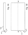
- FIGS 1A, 1B illustrate a semiconductor substrate 100.
- the semiconductor substrate 100 may be single material substrate or be formed of a combination of different materials, such as of various layers stacked on top of each other.
- at least an upper surface 100a of the substrate 100 is formed of an elemental group IV semiconductor or compound group IV semiconductor.
- the upper surface may be formed by a [111] face of silicon (Si).
- Possible substrate 100 structures include a Si substrate or a silicon-on-insulator (SOI) substrate.
- the upper surface 100a of the substrate 100 may be referred to as a front side surface of the substrate 100.
- a first partial insulating layer 102a has been formed on the upper surface 100a of the substrate 100.
- the first partial insulating layer 102a covers the upper surface 100a.
- the first partial insulating layer 102a may be an oxide layer, for instance a silicon oxide such as SiO 2 .
- the first partial insulating layer 102a may also be a dielectric layer of for instance a high-K dielectric material such as aluminum oxide or some other CMOS compatible gate dielectric.
- the first partial insulating layer 102a may be deposited on the surface 100a by any suitable and conventional deposition technique, such as chemical vapor deposition (CVD) or atomic layer deposition (ALD), or by thermal oxidation.
- CVD chemical vapor deposition
- ALD atomic layer deposition
- a trench 104 extending partially through the first partial insulating layer 102a has been formed.
- a longitudinal dimension of the trench 104 extends in the first horizontal direction X.
- a vertical dimension of the trench 104 extends in the vertical direction Z.
- a bottom surface of the trench 104 is formed by a remaining thickness portion of the first partial insulating layer 102a.
- a trench mask layer 103 has been formed on the first partial insulating layer 102a.
- a trench defining opening has been formed in the mask layer 103. The opening has subsequently been transferred into the first partial insulating layer 102a by etching of the material of the first partial insulating layer 102a to form the trench 104.
- the mask layer 103 may be a photo-resist based mask layer 103 of any other typical lithographic stack compatible with the material forming the first partial insulating layer 102a. Any conventional wet or dry etching process allowing etching of the material of the first partial insulating layer 102a may be employed. Subsequent to etching the trench 104, the mask layer 103 may be removed.
- the trench 104 may by way of example be formed with a width in the range of 20-100 nm, depending among others on the intended length of the final channel structure which is to be formed.
- a gate electrode 106 has been formed in the trench 104.
- the gate electrode 106 is elongated and extends along the substrate upper surface, in the first horizontal direction X.
- the gate electrode 106 is electrically insulated from the substrate 100 by the insulating layer 102.
- a conductive gate electrode material may be deposited in the trench 104.
- the conductive gate electrode material may be a metal or a metal alloy. However other gate electrode materials are also possible, such as polysilicon.
- the material may be deposited by any conventional deposition technique, such as by ALD, CVD or physical vapor deposition (PVD).
- the material may be deposited to fill the trench 104 and cover the first partial insulating layer 102a.
- Overburden gate electrode material i.e. material portions deposited outside of the trench 104) may subsequently be removed from outside of the trench by chemical mechanical polishing (CMP) and/or an etch back process, thereby exposing an upper surface of the insulating layer 102a.
- CMP
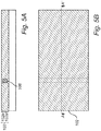
- the gate electrode 106 and the first partial insulating layer 102a has been covered by a second partial insulating layer 102b.
- the first partial insulating layer 102a and the second partial insulating layer 102b together form a compound insulating layer, hereinafter referred to as the insulating layer 102, embedding the gate electrode 106.
- the second partial insulating layer 102b may be formed of a same material as the first partial insulating layer 102a.
- the second partial insulating layer 102b may be deposited in a similar manner as the first partial insulating layer 102a.
- a total thickness of the insulating layer 102 may for instance be in the range of 10-50 nm.
- an aperture 108 has been formed in the insulating layer 102.
- the aperture 108 exposes an upper surface portion 100b (i.e. a portion of the upper surface 100a) of the substrate 100.
- the aperture 108 extends vertically through the insulating layer 102.
- An aperture mask layer 107 has been formed on the insulating layer 102.
- An aperture defining opening has been formed in the mask layer 107.
- the opening has subsequently been transferred into the insulating layer 102 by etching of the material (of the insulating layer 102 to form the aperture 108.
- the mask layer 107 may be a photo-resist based mask layer 107 of any other typical lithographic stack compatible with the material forming the first partial insulating layer 102a. Any conventional wet or dry etching process allowing etching of the material of the insulating layer 102 may be employed. Subsequent to etching the aperture 108 the mask layer 107 may be removed.
- a semiconductor structure 110 has been formed in an epitaxial growth process to include a group III-V semiconductor substrate contact part 112 and a group III-V semiconductor disc part 114.
- the substrate contact part 112 is formed in the aperture 108.
- the disc part 114 is formed above the insulating layer 102.
- the substrate contact part 112 has a bottom portion 112a abutting the upper surface portion 100b.
- the substrate contact part 112 has an upper portion 112b protruding from the aperture 108 above an upper surface 102c of the insulating layer 102.
- the disc part 114 extends from the upper portion 112b of the substrate contact part 112, horizontally or laterally along the upper surface 102c (i.e.
- the disc part 114 is accordingly formed to enclose the upper portion 112b of the substrate contact part 112 in a horizontal plane, or in other words enclose in a circumferential direction with respect to the substrate contact part 112. As may be seen in figures 7a and 7b a horizontal extension of the disc part 114 is such that the disc part 114 overlaps a portion 106a of the gate electrode 106.
- the semiconductor structure 110 may be formed by vapor phase epitaxy.
- a semiconductor structure 110 of any one of InSb, InAs, InGaAs or InGaSb may be epitaxially grown.
- the process conditions of the epitaxial process may be controlled such that at least the at least the disc part 114 is formed of monocrystalline material, for instance monocrystalline InSb, InAs, InGaAs or InGaSb.
- monocrystalline InSb, InAs, InGaAs or InGaSb for instance monocrystalline InSb, InAs, InGaAs or InGaSb.
- the epitaxial growth process may be adapted such that, for the group III-V semiconductor disc part 114, a growth rate in a horizontal plane (i.e. along the first and second horizontal directions X and Y) is greater than a growth rate in a vertical direction Z.
- the lateral/horizontal growth rate may for instance be (at least) a factor 10 greater than the vertical growth rate. This may be implemented during at least a part of the epitaxial growth process in which the disc part 114 is grown. However, as the lateral growth inside the aperture 108 will be limited by the lateral dimensions of the aperture 108 a lateral growth may be promoted throughout the epitaxial growth of the full semiconductor structure 110.
- a lateral growth of a group III-V semiconductor material may be obtained by controlling a growth temperature to be in the range of 500 °C to 650 °C.
- a total pressure (in the growth chamber) may be in the range of 20 mbar to 150 mbar.
- the process conditions during the growth may be controlled such that a lateral growth rate in the range of 1 nm/s to 5 nm/s, and a vertical growth rate in or below the range 0.1 nm/s to 0.5 nm/s is obtained.
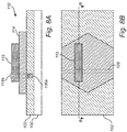
- a mask 115 has been formed on the semiconductor structure 110.
- the mask 115 may be referred to as the channel structure mask 115.
- the mask 115 covers a portion of the disc part 114.
- the masked portion may be formed as an elongated portion of the disc part 114, extending in the second horizontal direction Y.
- the portion (as well as the mask 115) includes a sub-portion 114a extending across the portion 106a of the gate electrode 106.
- the mask 115 may as shown in figure 9B be formed to expose the substrate contact part 112.
- the mask 115 may be formed by depositing a mask layer on the semiconductor structure 110, such as a photo-resist based mask layer or any other typical lithographic stack compatible with the material of the semiconductor structure 110.
- the mask 115 may subsequently be defined by patterning the mask layer using a conventional patterning technique.
- the regions of the semiconductor structure 110 exposed by the mask 115 have been etched such that the masked portion of the disc part 114 remains to form a channel structure 116.
- the channel structure 116 includes a portion 116a extending across the portion 106a of the gate electrode 106.
- the channel structure 116 extends along the upper surface of the insulating layer 102 to be elongated in the second horizontal direction Y.
- the mask 115 exposed the substrate contact part 112 the channel structure 116 is after completion of the etching disconnected from the substrate 100. Any remaining hole in the insulating layer 102 (i.e.
- the hole previously exposing the portion 100b and accommodating the substrate contact part 112) may for instance be filled by an insulating material subsequent to the etch.
- the semiconductor structure 110 may be etched using any conventional dry etching process allowing etching of the material of the semiconductor structure 110, such as a reactive ion etch (RIE) or ion beam etch (IBE). Subsequent to forming the channel structure 116 the mask 115 may be removed.
- RIE reactive ion etch
- IBE ion beam etch
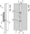
- a contact mask 118 (i.e. a source/drain contact mask 118) has been formed to cover the channel structure 116 and the insulating layer 102.
- the contact mask 118 may for instance be a resist-based mask or a PMMA mask.
- a source contact opening 118s exposing a source portion 116s of the channel structure 116 has been defined in the mask 118.
- a drain contact opening 118d exposing a drain portion 116d of the channel structure 116 has been defined in the mask 118.
- a superconductor source contact 120 and a superconductor drain contact 122 have been formed on the channel structure 116, at mutually opposite sides of the portion 106b of the gate electrode 106.
- a superconductor has been deposited in the source contact opening 118s and in the drain contact opening 118d.
- Al, Ta, Nd or Ti may be deposited by CVD, ALD or PVD.
- the superconductor may be deposited to fill the openings 118s and 118d and cover the contact mask 118.
- Overburden superconductor material may subsequently be removed from outside of the trench by CMP and/or an etch back process, thereby exposing an upper surface of the contact mask 118.
- the contact mask 118 may subsequently wherein the contacts 120, 122 may remain on the channel structure 116.
- the deposition of the superconductor in the contact openings 118s, 118d may be preceded by deposition of a superconductor seed layer (e.g. by selective area epitaxy) on portions of the channel structure 116 exposed in the contact openings 118s, 118d.
- a gate contact mask 124 has been formed to cover the channel structure 116, the contacts 120, 122 and the insulating layer 102.
- the gate contact mask 124 may for instance be a resist-based mask or a PMMA mask.
- a pair of gate contact openings 124a, 124b have been defined in the mask 124, exposing respective portions of the insulating layer directly above the gate electrode 106.
- a pair of gate contacts 126, 128 have been formed on mutually opposite sides of the channel structure 116.
- the gate contact openings 124a, 124b have been transferred into the insulating layer 102 to form a pair of gate contact holes in the insulating layer 102.
- the gate contact holes have subsequently been filled with a conductive contact material, for instance a metal such as a suitable CMOS-compatible metal contact material.
- the contact material may be deposited by CVD, ALD or PVD, for instance.
- Overburden contact material may subsequently be removed from outside of the gate contact holes by CMP and/or an etch back process, thereby exposing an upper surface of the gate contact mask 124.
- the mask 124 has subsequently been removed wherein the contacts 126, 128 remain on the gate electrode 106.
- the resulting device has a configuration which makes it suitable for use as a qubit device which, under the correct operating conditions as is known in the art, enables forming of Majorana fermions and conduction of the same along the channel structure 116 between the superconductor source and drain electrodes 120, 122.
- the configuration of the gate electrode 106 allows a chemical potential in the nanostructure 116 to be adapted to enable the Majorana fermions, i.e. qubits, to be manipulated.
- a plurality of such qubit may be formed on the substrate 100 and interconnected to each other to implement qubit logic gates.
- the channel structures may be formed to extend across a respective portion 106a of the gate electrode 106.
- the channel structures may be formed to extend in parallel to each other.
- More than one channel structure may be formed by patterning the channel structure mask (corresponding to mask 115 above) to include a number of discrete mask portions, each defining a respective channel structure.
- figure 14 illustrates a qubit device wherein additional embedded gate electrodes 206, 306, parallel to the gate electrode 106, have been formed along the channel structure 116.
- a respective further pair of gate contacts 226, 228 and 326, 328 have been formed on the gate contacts 206, 306.
- the further gate electrodes 206, 306 may be formed by forming further trenches parallel to the trench 104, as disclosed in connection with figures 3A and 3B .
- Three gate electrodes represents however only one example and a qubit device may be formed to include any number of embedded gate electrodes along the channel structure 116, however at least one.
Landscapes
- Engineering & Computer Science (AREA)
- Chemical & Material Sciences (AREA)
- Nanotechnology (AREA)
- Physics & Mathematics (AREA)
- Theoretical Computer Science (AREA)
- Mathematical Physics (AREA)
- Crystallography & Structural Chemistry (AREA)
- Materials Engineering (AREA)
- Insulated Gate Type Field-Effect Transistor (AREA)
- General Physics & Mathematics (AREA)
- Data Mining & Analysis (AREA)
- Evolutionary Computation (AREA)
- Condensed Matter Physics & Semiconductors (AREA)
- Mathematical Analysis (AREA)
- Mathematical Optimization (AREA)
- Pure & Applied Mathematics (AREA)
- Computing Systems (AREA)
- General Engineering & Computer Science (AREA)
- Software Systems (AREA)
- Computational Mathematics (AREA)
- Artificial Intelligence (AREA)
- Thin Film Transistor (AREA)
- Semiconductor Memories (AREA)
Abstract
Description
- The present inventive concept relates to a method for forming a qubit device. The present inventive concept further relates to a qubit device.
- Quantum information science has the potential to radically improve existing techniques and devices for sensing, computation, simulation, and communication.
- A major challenge in quantum information processing systems is to realize qubits with a sufficient degree of coherence while still allowing manipulation and measurements. One type of qubit device showing promise are devices based on so-called Majorana fermions. A Majorana fermion is its own antiparticle and may in a quantum mechanical framework be described as a superposition of an electron and a hole.
- Although qubit devices based on Majorana fermions have been demonstrated on a lab-scale, realizing industrially viable and scalable qubit devices remains a challenge. Therefore, quantum information processing experiments are still expensive and time consuming endeavors. Existing laboratory setups may also be challenging to fine tune and scale.
- An objective of the present inventive concept is to address this issue in the prior art. Further and alternative objectives may be understood from the following.
- According to an aspect of the present inventive concept there is provided a method for forming a qubit device, the method comprising:
- forming a gate electrode embedded in an insulating layer formed on a substrate, wherein an upper surface of the substrate is formed by a group IV semiconductor material and wherein the gate electrode extends along the substrate in a first horizontal direction,
- forming an aperture in the insulating layer, the aperture exposing a portion of the substrate,
- forming in an epitaxial growth process, a semiconductor structure comprising a group III-V semiconductor substrate contact part and a group III-V semiconductor disc part,
- the substrate contact part having a bottom portion abutting said portion of the substrate and an upper portion protruding from the aperture above an upper surface of the insulating layer,
- the semiconductor disc part extending from said upper portion of the substrate contact part, horizontally along said upper surface of the insulating layer to overlap a portion of the gate electrode,
- forming a mask covering a portion of the disc part, said portion of the disc part extending across said portion of the gate electrode in a second horizontal direction,
- etching regions of the semiconductor structure exposed by the mask such that the masked portion of the disc part remains to form a channel structure extending across said portion of the gate electrode, and
- forming a superconductor source contact and a superconductor drain contact for contacting the channel structure at mutually opposite sides of said portion of the gate electrode.
- The inventive method enables accurate, repeatable and scalable manufacturing of qubit devices. The combination of a group III-V semiconductor channel structure and superconductor source and drain contacts enable Majorana fermion based qubit devices. By qubit device is hereby meant a semiconductor device with a configuration such that, under the correct operating conditions, it may support or provide states or particles (or more specifically quasiparticles in the case of Majorana fermions) which may operate as qubits whose state may be manipulated and detected.
- As the channel structure is formed by patterning an epitaxially grown group III-V material structure the typical prior art approach of growing nanostructures (such as vertical nanowires) on a separate wafer and thereafter transferring them to a target substrate may be avoided. The method thereby allows an overall more efficient process as transfer of nanowires to intended positions at a target substrate may be delicate and difficult to scale.
- Furthermore, the forming of the channel structure by patterning allows a considerable degree of control of the dimension, shape and arrangement of the channel structure in relation to the gate electrode.
- By forming the gate electrode as an embedded gate electrode, exposure of the channel structure to the potentially adverse process conditions of gate electrode and gate dielectric formation may be avoided. Moreover, the embedded configuration of the gate electrode enables a gate-channel coupling of a strength suitable for qubit device operation to be achieved.
- In terms of device properties, the method enables scalable fabrication of qubit devices with an improved uniformity in terms of structure and performance.
- The superconductor source contact and the superconductor drain contact are advantageously formed subsequent to forming the channel structure. More specifically, the method may comprise forming the superconductor source contact and the superconductor drain contact on the channel structure at mutually opposite sides of said portion of the gate electrode. This facilitates achieving a proper alignment between the source/drain portions of the channel structure and the source/drain contacts.
- By the upper surface of the substrate is intended a main surface of the substrate on which the processing according to the inventive method is performed. Hence, "upper" should not be construed to require a particular orientation of the substrate.
- As used herein, the term first horizontal direction refers to a direction along the substrate, i.e. along the upper surface of the substrate. Correspondingly, the second horizontal direction refers to a direction along the substrate, which second horizontal direction is different from the first horizontal direction. The first and second horizontal directions may represent mutually perpendicular directions but may more generally extend at an angle with respect to each other. Accordingly, the term horizontal plane may be used to refer to a plane defined by the first and second horizontal directions. In other words, the term horizontal plane may denote a plane parallel to the upper (main) surface of the substrate.
- A vertical direction may refer to a direction which is normal to the upper (main) surface of the substrate, or perpendicular to the first and second horizontal directions.
- By a superconductor is hereby meant any material exhibiting superconductivity when kept at a temperature below a critical temperature Tc, specific to the material. By way of example, Tc of Al is 1.20 K, Tc of Ta is 4.48 K and Tc of Ti is 0.39 K, Tc of Nd is 9.26 K.
- The mask may be formed such that the substrate contact part is exposed by the mask. Accordingly the substrate contact part may be removed during the etching wherein the channel structure is electrically insulated from the substrate by the insulator layer.
- According to one embodiment, said forming of the gate electrode embedded in the insulating layer comprises:
- forming a first partial insulating layer on the upper surface of the substrate,
- forming a trench extending partially through the first partial insulating layer,
- forming the gate electrode in the trench, and
- covering the gate electrode and the first partial insulating layer with a second partial insulating layer, wherein the first partial insulating layer and the second partial insulating layer together forms said insulating layer. As the trench is formed to extend only partially through the insulating layer, the gate electrode may be formed on an electrically insulating bottom surface of the trench.
- The gate electrode may be formed to be elongated in the first horizontal direction. An elongated gate electrode enables definition of a short gate-channel interface, along the direction of the channel. A highly localized gate control may thereby be achieved.
- The method may further comprise forming a pair of gate contacts on the gate electrode, at mutually opposite sides of the channel structure . Easy accessible electrical contact to the gate electrode may thereby be provided. In case the gate electrode is formed to be elongated the contacts may be formed spaced apart from the channel structure to mitigate undesired stray capacitive coupling between the contacts and the channel.
- According to one embodiment said gate electrode forms a first gate electrode and the method further comprises forming at least a second gate electrode, each one of the gate electrodes being embedded in the insulating layer and extending in said first direction. Providing more than gate electrode enables improved channel control along the length of the channel structure.
- The semiconductor disc part may be formed to overlap a respective portion of each one of the gate electrodes, wherein the channel structure may extend across each one of said portions of the gate electrodes. Gate electrode-channel structure overlap may thereby be obtained at plural positions in an efficient manner.
- The epitaxial growth process may be adapted such that a growth rate in a horizontal plane is greater than a growth rate in a vertical direction during a part of the epitaxial growth process in which the disc part is grown. Thereby a disc part having a greater horizontal dimension than vertical dimension may be grown. This in turn enables forming of a relatively long and thin channel structure.
- The channel structure may be formed to be elongated in the second horizontal direction. Combined with an epitaxial growth process promoting a horizontal plane growth rate a channel structure having a high length to thickness ratio and, optionally, a high width to thickness ratio may be achieved. Such a channel structure may be referred to as a nanowire.
- The disc part may be formed to enclose the upper portion of the substrate contact part in a horizontal plane. The channel structure may hence be formed to extend on either side of the substrate contact part.
- According to one embodiment the forming of the source and drain superconductor contacts may comprise:
- forming a contact mask including a source contact opening exposing a source portion of the channel structure, and further including a drain contact opening exposing a drain portion of the channel structure, and
- forming the source superconductor contact in the source contact opening and the drain superconductor contact in the drain contact opening.
- Superconductor contacts may thereby be conveniently formed wherein portions of the channel structure covered by the contact mask (i.e. portions other than the source portion and the drain portion) may be protected, at least to some extent, from the process conditions of the contact formation. The forming of the source and drain superconductor contacts in the respective mask openings may include deposition of a superconductor material in the respective openings. Optionally, a superconductor seed layer may be formed on portions of the channel structure exposed in the contact openings. This may improve an interface quality between the superconductor source/drain contacts and the channel structure.
- The superconductor source contact and the superconductor drain contact may include, or consist of, Al, Ta, Ti or Nd.
- The epitaxial growth process may comprise growing the semiconductor structure of InSb, InAs, InGaAs or InGaSb. These semiconductor materials, when used in combination with superconductor contacts, enable formation of Majorana fermions in the device channel.
- Advantageously, to enable improved device operation, at least the disc part may be formed of monocrystalline InSb, InAs, InGaAs or InGaSb.
- According to another aspect of the present inventive concept there is provided a qubit device comprising:
- a gate electrode embedded in an insulating layer formed on a substrate, wherein an upper surface of the substrate is formed by a group IV semiconductor material and wherein the gate electrode extends along the substrate in a first horizontal direction,
- a group III-V semiconductor channel structure extending horizontally, in a second horizontal direction, along an upper surface of the insulating layer and across a portion of the gate electrode, and
- a superconductor source contact and a superconductor drain contact formed on the channel structure at mutually opposite sides of said portion of the gate electrode.
- According to another aspect of the present inventive concept there is provided a qubit device manufactured or obtained in accordance with the method of any of the above described embodiments and variations thereof. These further aspects may generally present the same or corresponding advantages as the former method aspect.
- The above, as well as additional objects, features and advantages of the present inventive concept, will be better understood through the following illustrative and non-limiting detailed description, with reference to the appended drawings. In the drawings like reference numerals will be used for like elements unless stated otherwise.
-
Figures 1-13 schematically illustrate a method for forming a qubit device. -
Figure 14 schematically shows a variation of a qubit device. - A method for forming a qubit device will now be disclosed in connection with
figures 1-13 . Each one of the figures shows a cross-sectional side view (figure a) of the structure and a top down view (figure b). The cross-sectional view in figure A is taken along the geometrical line indicated in the correspondingly numbered figure B (i.e. line AA' or BB'). In the figures the axis Z denotes a vertical direction, corresponding to a normal direction with respect to anupper surface 100a of asubstrate 100. The axes X and Y refer to mutually orthogonal first and second horizontal directions, i.e. directions being parallel to the main plane of extension of the substrate 100 (or correspondingly theupper surface 100a thereof). It should be noted that the relative dimensions of the shown elements, such as the relative thickness of the layers of structures, is merely schematic and may, for the purpose of illustrational clarity, differ from a physical structure. -
Figures 1A, 1B illustrate asemiconductor substrate 100. Thesemiconductor substrate 100 may be single material substrate or be formed of a combination of different materials, such as of various layers stacked on top of each other. In any case at least anupper surface 100a of thesubstrate 100 is formed of an elemental group IV semiconductor or compound group IV semiconductor. The upper surface may be formed by a [111] face of silicon (Si).Possible substrate 100 structures include a Si substrate or a silicon-on-insulator (SOI) substrate. Theupper surface 100a of thesubstrate 100 may be referred to as a front side surface of thesubstrate 100. - In
figures 2A, 2B a first partial insulatinglayer 102a has been formed on theupper surface 100a of thesubstrate 100. The first partial insulatinglayer 102a covers theupper surface 100a. The first partial insulatinglayer 102a may be an oxide layer, for instance a silicon oxide such as SiO2. The first partial insulatinglayer 102a may also be a dielectric layer of for instance a high-K dielectric material such as aluminum oxide or some other CMOS compatible gate dielectric. The first partial insulatinglayer 102a may be deposited on thesurface 100a by any suitable and conventional deposition technique, such as chemical vapor deposition (CVD) or atomic layer deposition (ALD), or by thermal oxidation. - In
figures 3A, 3B atrench 104 extending partially through the first partial insulatinglayer 102a has been formed. A longitudinal dimension of thetrench 104 extends in the first horizontal direction X. A vertical dimension of thetrench 104 extends in the vertical direction Z. As indicated infigures 3A, 3B a bottom surface of thetrench 104 is formed by a remaining thickness portion of the first partial insulatinglayer 102a. Atrench mask layer 103 has been formed on the first partial insulatinglayer 102a. A trench defining opening has been formed in themask layer 103. The opening has subsequently been transferred into the first partial insulatinglayer 102a by etching of the material of the first partial insulatinglayer 102a to form thetrench 104. Themask layer 103 may be a photo-resist basedmask layer 103 of any other typical lithographic stack compatible with the material forming the first partial insulatinglayer 102a. Any conventional wet or dry etching process allowing etching of the material of the first partial insulatinglayer 102a may be employed. Subsequent to etching thetrench 104, themask layer 103 may be removed. Thetrench 104 may by way of example be formed with a width in the range of 20-100 nm, depending among others on the intended length of the final channel structure which is to be formed. - In
figures 4A, 4B , agate electrode 106 has been formed in thetrench 104. Thegate electrode 106 is elongated and extends along the substrate upper surface, in the first horizontal direction X. Thegate electrode 106 is electrically insulated from thesubstrate 100 by the insulatinglayer 102. A conductive gate electrode material may be deposited in thetrench 104. The conductive gate electrode material may be a metal or a metal alloy. However other gate electrode materials are also possible, such as polysilicon. The material may be deposited by any conventional deposition technique, such as by ALD, CVD or physical vapor deposition (PVD). The material may be deposited to fill thetrench 104 and cover the first partial insulatinglayer 102a. Overburden gate electrode material (i.e. material portions deposited outside of the trench 104) may subsequently be removed from outside of the trench by chemical mechanical polishing (CMP) and/or an etch back process, thereby exposing an upper surface of the insulatinglayer 102a. - In
figures 5A, 5B , thegate electrode 106 and the first partial insulatinglayer 102a has been covered by a second partial insulatinglayer 102b. The first partial insulatinglayer 102a and the second partial insulatinglayer 102b together form a compound insulating layer, hereinafter referred to as the insulatinglayer 102, embedding thegate electrode 106. The second partial insulatinglayer 102b may be formed of a same material as the first partial insulatinglayer 102a. The second partial insulatinglayer 102b may be deposited in a similar manner as the first partial insulatinglayer 102a. A total thickness of the insulatinglayer 102 may for instance be in the range of 10-50 nm. - In
figures 6A, 6B , anaperture 108 has been formed in the insulatinglayer 102. Theaperture 108 exposes anupper surface portion 100b (i.e. a portion of theupper surface 100a) of thesubstrate 100. Theaperture 108 extends vertically through the insulatinglayer 102. Anaperture mask layer 107 has been formed on the insulatinglayer 102. An aperture defining opening has been formed in themask layer 107. The opening has subsequently been transferred into the insulatinglayer 102 by etching of the material (of the insulatinglayer 102 to form theaperture 108. Themask layer 107 may be a photo-resist basedmask layer 107 of any other typical lithographic stack compatible with the material forming the first partial insulatinglayer 102a. Any conventional wet or dry etching process allowing etching of the material of the insulatinglayer 102 may be employed. Subsequent to etching theaperture 108 themask layer 107 may be removed. - In
figures 7A, 7B , asemiconductor structure 110 has been formed in an epitaxial growth process to include a group III-V semiconductorsubstrate contact part 112 and a group III-Vsemiconductor disc part 114. Thesubstrate contact part 112 is formed in theaperture 108. Thedisc part 114 is formed above the insulatinglayer 102. Thesubstrate contact part 112 has abottom portion 112a abutting theupper surface portion 100b. Thesubstrate contact part 112 has anupper portion 112b protruding from theaperture 108 above anupper surface 102c of the insulatinglayer 102. Thedisc part 114 extends from theupper portion 112b of thesubstrate contact part 112, horizontally or laterally along theupper surface 102c (i.e. in the horizontal plane defined by the axes X and Y). Thedisc part 114 is accordingly formed to enclose theupper portion 112b of thesubstrate contact part 112 in a horizontal plane, or in other words enclose in a circumferential direction with respect to thesubstrate contact part 112. As may be seen infigures 7a and 7b a horizontal extension of thedisc part 114 is such that thedisc part 114 overlaps aportion 106a of thegate electrode 106. Thesemiconductor structure 110 may be formed by vapor phase epitaxy. - It should be noted that the particular polygonal shape of the
disc part 114 illustrated infigure 7b merely is one example and that other shapes, such as generally hexagonal shapes, also are possible. The specific shape typically may depend on the growth conditions and the orientation of the growth surfaces. - A
semiconductor structure 110 of any one of InSb, InAs, InGaAs or InGaSb may be epitaxially grown. The process conditions of the epitaxial process may be controlled such that at least the at least thedisc part 114 is formed of monocrystalline material, for instance monocrystalline InSb, InAs, InGaAs or InGaSb. However, it may also be possible to use other materials with a sufficiently large Lande G-factor. - The epitaxial growth process may be adapted such that, for the group III-V
semiconductor disc part 114, a growth rate in a horizontal plane (i.e. along the first and second horizontal directions X and Y) is greater than a growth rate in a vertical direction Z. The lateral/horizontal growth rate may for instance be (at least) a factor 10 greater than the vertical growth rate. This may be implemented during at least a part of the epitaxial growth process in which thedisc part 114 is grown. However, as the lateral growth inside theaperture 108 will be limited by the lateral dimensions of the aperture 108 a lateral growth may be promoted throughout the epitaxial growth of thefull semiconductor structure 110. - For instance, a lateral growth of a group III-V semiconductor material may be obtained by controlling a growth temperature to be in the range of 500 °C to 650 °C. A total pressure (in the growth chamber) may be in the range of 20 mbar to 150 mbar. The process conditions during the growth may be controlled such that a lateral growth rate in the range of 1 nm/s to 5 nm/s, and a vertical growth rate in or below the range 0.1 nm/s to 0.5 nm/s is obtained.
- In
figures 8A, 8B amask 115 has been formed on thesemiconductor structure 110. Themask 115 may be referred to as thechannel structure mask 115. Themask 115 covers a portion of thedisc part 114. The masked portion may be formed as an elongated portion of thedisc part 114, extending in the second horizontal direction Y. The portion (as well as the mask 115) includes a sub-portion 114a extending across theportion 106a of thegate electrode 106. Themask 115 may as shown infigure 9B be formed to expose thesubstrate contact part 112. Themask 115 may be formed by depositing a mask layer on thesemiconductor structure 110, such as a photo-resist based mask layer or any other typical lithographic stack compatible with the material of thesemiconductor structure 110. Themask 115 may subsequently be defined by patterning the mask layer using a conventional patterning technique. - In
figures 9A, 9B the regions of thesemiconductor structure 110 exposed by themask 115 have been etched such that the masked portion of thedisc part 114 remains to form achannel structure 116. As shown infigures 9A, 9B thechannel structure 116 includes aportion 116a extending across theportion 106a of thegate electrode 106. Thechannel structure 116 extends along the upper surface of the insulatinglayer 102 to be elongated in the second horizontal direction Y. As themask 115 exposed thesubstrate contact part 112 thechannel structure 116 is after completion of the etching disconnected from thesubstrate 100. Any remaining hole in the insulating layer 102 (i.e. the hole previously exposing theportion 100b and accommodating the substrate contact part 112) may for instance be filled by an insulating material subsequent to the etch. Thesemiconductor structure 110 may be etched using any conventional dry etching process allowing etching of the material of thesemiconductor structure 110, such as a reactive ion etch (RIE) or ion beam etch (IBE). Subsequent to forming thechannel structure 116 themask 115 may be removed. - In
figures 10A, 10B a contact mask 118 (i.e. a source/drain contact mask 118) has been formed to cover thechannel structure 116 and the insulatinglayer 102. Thecontact mask 118 may for instance be a resist-based mask or a PMMA mask. A source contact opening 118s exposing asource portion 116s of thechannel structure 116 has been defined in themask 118. Further, adrain contact opening 118d exposing adrain portion 116d of thechannel structure 116 has been defined in themask 118. - In
figures 11A, 11B asuperconductor source contact 120 and asuperconductor drain contact 122 have been formed on thechannel structure 116, at mutually opposite sides of the portion 106b of thegate electrode 106. A superconductor has been deposited in the source contact opening 118s and in thedrain contact opening 118d. For instance Al, Ta, Nd or Ti may be deposited by CVD, ALD or PVD. The superconductor may be deposited to fill theopenings contact mask 118. Overburden superconductor material may subsequently be removed from outside of the trench by CMP and/or an etch back process, thereby exposing an upper surface of thecontact mask 118. Thecontact mask 118 may subsequently wherein thecontacts channel structure 116. Optionally, the deposition of the superconductor in thecontact openings channel structure 116 exposed in thecontact openings - In
figures 12A, 12B agate contact mask 124 has been formed to cover thechannel structure 116, thecontacts layer 102. Thegate contact mask 124 may for instance be a resist-based mask or a PMMA mask. A pair ofgate contact openings mask 124, exposing respective portions of the insulating layer directly above thegate electrode 106. - In
figures 13A, 13B , a pair ofgate contacts channel structure 116. Thegate contact openings layer 102 to form a pair of gate contact holes in the insulatinglayer 102. The gate contact holes have subsequently been filled with a conductive contact material, for instance a metal such as a suitable CMOS-compatible metal contact material. The contact material may be deposited by CVD, ALD or PVD, for instance. Overburden contact material may subsequently be removed from outside of the gate contact holes by CMP and/or an etch back process, thereby exposing an upper surface of thegate contact mask 124. Themask 124 has subsequently been removed wherein thecontacts gate electrode 106. - The resulting device has a configuration which makes it suitable for use as a qubit device which, under the correct operating conditions as is known in the art, enables forming of Majorana fermions and conduction of the same along the
channel structure 116 between the superconductor source and drainelectrodes gate electrode 106 allows a chemical potential in thenanostructure 116 to be adapted to enable the Majorana fermions, i.e. qubits, to be manipulated. Advantageously, a plurality of such qubit may be formed on thesubstrate 100 and interconnected to each other to implement qubit logic gates. - In the above the inventive concept has mainly been described with reference to a limited number of examples. However, as is readily appreciated by a person skilled in the art, other examples than the ones disclosed above are equally possible within the scope of the inventive concept, as defined by the appended claims.
- For instance, it is possible to form more than one, such as two or more, channel structures simultaneously from the
disc part 114. The channel structures may be formed to extend across arespective portion 106a of thegate electrode 106. The channel structures may be formed to extend in parallel to each other. More than one channel structure may be formed by patterning the channel structure mask (corresponding to mask 115 above) to include a number of discrete mask portions, each defining a respective channel structure. - According to a further variation,
figure 14 illustrates a qubit device wherein additional embeddedgate electrodes gate electrode 106, have been formed along thechannel structure 116. A respective further pair ofgate contacts gate contacts further gate electrodes trench 104, as disclosed in connection withfigures 3A and 3B . Three gate electrodes represents however only one example and a qubit device may be formed to include any number of embedded gate electrodes along thechannel structure 116, however at least one.
Claims (15)
- A method for forming a qubit device, the method comprising:forming a gate electrode (106) embedded in an insulating layer (102) formed on a substrate (100), wherein an upper surface (100a) of the substrate (100) is formed by a group IV semiconductor material and wherein the gate electrode (106) extends along the substrate (100) in a first horizontal direction,forming an aperture (108) in the insulating layer (102), the aperture (108) exposing a portion (100b) of the substrate (100),forming in an epitaxial growth process, a semiconductor structure (110) comprising a group III-V semiconductor substrate contact part (112) and a group III-V semiconductor disc part (114),the substrate contact part (112) having a bottom portion (112a) abutting said portion (100b) of the substrate (100) and an upper portion (112b) protruding from the aperture (108) above an upper surface (102c) of the insulating layer (102),the semiconductor disc part (114) extending from said upper portion (112b) of the substrate contact part (112), horizontally along said upper surface (102c) of the insulating layer (102) to overlap a portion (106a) of the gate electrode (106),forming a mask (115) covering a portion of the disc part (114), said portion of the disc part (114) extending across said portion (106a) of the gate electrode (106) in a second horizontal direction,etching regions of the semiconductor structure (110) exposed by the mask (115) such that the masked portion of the disc part (114) remains to form a channel structure (116) extending across said portion (106a) of the gate electrode (106), andforming a superconductor source contact (120) and a superconductor drain contact (122) on the channel structure (116) at mutually opposite sides of said portion (106b) of the gate electrode (106).
- A method according to claim 1, wherein the substrate contact part (112) is exposed by said mask (115).
- A method according to any of the preceding claims, said forming of the gate electrode (106) embedded in the insulating layer (102) comprises:forming a first partial insulating layer (102a) on the upper surface (100a) of the substrate (100),forming a trench (104) extending partially through the first partial insulating layer (102a),forming the gate electrode (106) in the trench (104), andcovering the gate electrode (106) and the first partial insulating layer (102a) with a second partial insulating layer (102b), wherein the first partial insulating layer (102a) and the second partial insulating layer (102b) together forms said insulating layer (102).
- A method according to any of the preceding claims, further comprising forming a pair of gate contacts (126, 128) on the gate electrode (106), at mutually opposite sides of the channel structure (116).
- A method according to any of the preceding claims, wherein the gate electrode (106) is formed to be elongated in the first horizontal direction.
- A method according to any of claims 3-5, wherein said gate electrode (106) forms a first gate electrode (106) and the method further comprises forming at least a second gate electrode (206), each gate electrode (106, 206) being embedded in the insulating layer (102) and extending in said first direction.
- A method according to claim 6, wherein the semiconductor disc part (114) is formed to overlap a respective portion of each one of the gate electrodes (106, 206), and wherein the channel structure (116) extends across each one of said portions of the gate electrodes (106, 206).
- A method according to any of the preceding claims, wherein the epitaxial growth process is adapted such that a growth rate in a horizontal plane is greater than a growth rate in a vertical direction during a part of the epitaxial growth process in which the disc part (114) is grown.
- A method according to any of the preceding claims, wherein the channel structure (116) is formed to be elongated in the second horizontal direction.
- A method according to any of the preceding claims, wherein the disc part (114) is formed to enclose the upper portion (112b) of the substrate contact part (112) in a horizontal plane.
- A method according to any of the preceding claims, wherein the forming of the source and drain superconductor contacts (120, 122) comprises:forming a contact mask (118) including a source contact opening (118s) exposing a source portion (116s) of the channel structure (116), and further including a drain contact opening (118d) exposing a drain portion (116d) of the channel structure (116), andforming the source superconductor contact in the source contact opening (118s) and the drain superconductor contact in the drain contact opening (118d).
- A method according to any of the preceding claims, wherein the superconductor source contact (120) and the superconductor drain contact (122) includes Al, Ta, Ti or Nd.
- A method according to any of the preceding claims, wherein the epitaxial growth process comprises growing the semiconductor structure (110) of InSb, InAs, InGaAs or InGaSb.
- A method according to claim 13, wherein at least the disc part (114) is formed of monocrystalline InSb, InAs, InGaAs or InGaSb.
- A qubit device comprising:a gate electrode (106) embedded in an insulating layer (102) formed on a substrate (100), wherein an upper surface (100a) of the substrate (100) is formed by a group IV semiconductor material and wherein the gate electrode (106) extends along the substrate (100) in a first horizontal direction,a group III-V semiconductor channel structure (116) extending horizontally, in a second horizontal direction, along an upper surface (102c) of the insulating layer (102) across a portion (106a) of the gate electrode (106), anda superconductor source contact (120) and a superconductor drain contact (122) formed on the channel structure (116) at mutually opposite sides of said portion (106b) of the gate electrode (106).
Priority Applications (3)
| Application Number | Priority Date | Filing Date | Title |
|---|---|---|---|
| EP17211120.5A EP3505490B1 (en) | 2017-12-29 | 2017-12-29 | A method for forming a qubit device |
| US16/222,911 US10930750B2 (en) | 2017-12-29 | 2018-12-17 | Method for forming a qubit device |
| CN201811590556.5A CN110009107B (en) | 2017-12-29 | 2018-12-20 | A method for forming qubit devices |
Applications Claiming Priority (1)
| Application Number | Priority Date | Filing Date | Title |
|---|---|---|---|
| EP17211120.5A EP3505490B1 (en) | 2017-12-29 | 2017-12-29 | A method for forming a qubit device |
Publications (2)
| Publication Number | Publication Date |
|---|---|
| EP3505490A1 true EP3505490A1 (en) | 2019-07-03 |
| EP3505490B1 EP3505490B1 (en) | 2022-02-09 |
Family
ID=60937584
Family Applications (1)
| Application Number | Title | Priority Date | Filing Date |
|---|---|---|---|
| EP17211120.5A Active EP3505490B1 (en) | 2017-12-29 | 2017-12-29 | A method for forming a qubit device |
Country Status (3)
| Country | Link |
|---|---|
| US (1) | US10930750B2 (en) |
| EP (1) | EP3505490B1 (en) |
| CN (1) | CN110009107B (en) |
Cited By (13)
| Publication number | Priority date | Publication date | Assignee | Title |
|---|---|---|---|---|
| WO2021126385A1 (en) * | 2019-12-16 | 2021-06-24 | Microsoft Technology Licensing, Llc | Josephson magnetic memory with a semiconductor-based magnetic spin valve |
| US20210193897A1 (en) * | 2019-09-11 | 2021-06-24 | International Business Machines Corporation | Combined dolan bridge and quantum dot josephson junction in series |
| WO2021197573A1 (en) * | 2020-03-30 | 2021-10-07 | Microsoft Technology Licensing Llc | Method of fabricating gates |
| WO2021197590A1 (en) * | 2020-03-31 | 2021-10-07 | Microsoft Technology Licensing Llc | Side-gated semiconduductor-superconductor hybrid devices |
| US11203526B2 (en) | 2018-06-20 | 2021-12-21 | equal1.labs Inc. | Reprogrammable quantum processor architecture incorporating quantum error correction |
| US11380836B2 (en) | 2020-03-16 | 2022-07-05 | International Business Machines Corporation | Topological qubit device |
| CN114730793A (en) * | 2019-11-19 | 2022-07-08 | 国际商业机器公司 | Ion implantation-defined nanorods in suspended Macjorana fermion devices |
| US11423322B2 (en) | 2018-06-20 | 2022-08-23 | equal1.labs Inc. | Integrated quantum computer incorporating quantum core and associated classical control circuitry |
| US11450760B2 (en) | 2018-06-20 | 2022-09-20 | equal1.labs Inc. | Quantum structures using aperture channel tunneling through depletion region |
| US11533046B2 (en) | 2020-11-12 | 2022-12-20 | equal1.labs Inc. | System and method of generating quantum unitary noise using silicon based quantum dot arrays |
| WO2023274511A1 (en) * | 2021-06-29 | 2023-01-05 | Microsoft Technology Licensing Llc | Semiconductor device having an electrostatically-bounded active region |
| WO2023284936A1 (en) * | 2021-07-12 | 2023-01-19 | Microsoft Technology Licensing Llc | Semiconductor-superconductor hybrid device including an electrode array |
| US11611032B2 (en) | 2018-06-20 | 2023-03-21 | equal1.labs Inc. | Semiconductor process optimized for quantum structures |
Families Citing this family (4)
| Publication number | Priority date | Publication date | Assignee | Title |
|---|---|---|---|---|
| US11793089B2 (en) * | 2019-09-20 | 2023-10-17 | Microsoft Technology Licensing, Llc | Durable hybrid heterostructures and methods for manufacturing the same |
| US20220393091A1 (en) * | 2019-11-11 | 2022-12-08 | The Trustees Of Princeton University | Superconducting qubits based on tantalum |
| US11563162B2 (en) * | 2020-01-09 | 2023-01-24 | International Business Machines Corporation | Epitaxial Josephson junction transmon device |
| CN114256407B (en) * | 2020-09-25 | 2023-08-08 | 本源量子计算科技(合肥)股份有限公司 | Preparation method of two Josephson junctions connected in parallel and qubit device |
Citations (1)
| Publication number | Priority date | Publication date | Assignee | Title |
|---|---|---|---|---|
| WO2016000836A1 (en) * | 2014-07-02 | 2016-01-07 | University Of Copenhagen | A semiconductor josephson junction and a transmon qubit related thereto |
Family Cites Families (23)
| Publication number | Priority date | Publication date | Assignee | Title |
|---|---|---|---|---|
| CA2051048C (en) * | 1990-09-10 | 1996-07-02 | Takao Nakamura | Superconducting device having a reduced thickness of oxide superconducting layer and method for manufacturing the same |
| JPH08288563A (en) * | 1995-04-17 | 1996-11-01 | Sumitomo Electric Ind Ltd | Superconducting field effect device and method of manufacturing the same |
| US6979836B2 (en) * | 2001-08-29 | 2005-12-27 | D-Wave Systems, Inc. | Superconducting low inductance qubit |
| US20030102470A1 (en) * | 2001-08-30 | 2003-06-05 | Evgeni Il'ichev | Oxygen doping of josephson junctions |
| US7385262B2 (en) * | 2001-11-27 | 2008-06-10 | The Board Of Trustees Of The Leland Stanford Junior University | Band-structure modulation of nano-structures in an electric field |
| US7138316B2 (en) | 2003-09-23 | 2006-11-21 | Intel Corporation | Semiconductor channel on insulator structure |
| JP4836064B2 (en) * | 2004-08-16 | 2011-12-14 | 独立行政法人理化学研究所 | Quantum state readout circuit |
| US20070296052A1 (en) * | 2006-06-26 | 2007-12-27 | Taiwan Semiconductor Manufacturing Company, Ltd. | Methods of forming silicide regions and resulting MOS devices |
| US8183587B2 (en) * | 2006-12-22 | 2012-05-22 | Qunano Ab | LED with upstanding nanowire structure and method of producing such |
| GB0801494D0 (en) * | 2007-02-23 | 2008-03-05 | Univ Ind & Acad Collaboration | Nonvolatile memory electronic device using nanowire used as charge channel and nanoparticles used as charge trap and method for manufacturing the same |
| CN105264680B (en) * | 2011-03-30 | 2019-11-26 | 阿姆巴托雷股份有限公司 | Electrical, mechanical, computing and/or other devices formed from extremely low-resistance materials |
| WO2013082117A1 (en) * | 2011-11-28 | 2013-06-06 | Michigan Technological University | Room temperature tunneling switches and methods of making and using the same |
| US9082746B2 (en) * | 2012-01-16 | 2015-07-14 | Infineon Technologies Austria Ag | Method for forming self-aligned trench contacts of semiconductor components and a semiconductor component |
| KR102130139B1 (en) * | 2013-07-30 | 2020-07-03 | 엘지디스플레이 주식회사 | Organic Light Emitting Diode Display Having Thin Film Transistor Substrate Using Oxide Semiconductor And Method For Manufacturing The Same |
| US9121820B2 (en) * | 2013-08-23 | 2015-09-01 | Taiwan Semiconductor Manufacturing Co., Ltd. | Top-down fabrication method for forming a nanowire transistor device |
| CN104157785A (en) * | 2014-07-30 | 2014-11-19 | 长沙理工大学 | Method capable of improving spin filtering effect of graphene nanometer device |
| US9576796B2 (en) * | 2015-05-15 | 2017-02-21 | Taiwan Semiconductor Manufacturing Company, Ltd. | Semiconductor devices and methods of manufacture thereof |
| US9755133B1 (en) * | 2016-03-03 | 2017-09-05 | The United States Of America As Represented By Secretary Of The Navy | Reconfigurable, tunable quantum qubit circuits with internal, nonvolatile memory |
| US9437614B1 (en) * | 2015-09-18 | 2016-09-06 | International Business Machines Corporation | Dual-semiconductor complementary metal-oxide-semiconductor device |
| US20190164959A1 (en) * | 2016-09-29 | 2019-05-30 | Intel Corporation | On-chip control logic for qubits |
| CN107170813B (en) * | 2017-06-26 | 2023-08-29 | 中国科学技术大学 | Hole type semiconductor electric control quantum dot device and preparation and use methods thereof |
| US10490727B2 (en) * | 2018-02-20 | 2019-11-26 | Intel Corporation | Gate arrangements in quantum dot devices |
| US10850978B2 (en) * | 2018-06-20 | 2020-12-01 | equal1.labs Inc. | Quantum shift register structures |
-
2017
- 2017-12-29 EP EP17211120.5A patent/EP3505490B1/en active Active
-
2018
- 2018-12-17 US US16/222,911 patent/US10930750B2/en active Active
- 2018-12-20 CN CN201811590556.5A patent/CN110009107B/en active Active
Patent Citations (1)
| Publication number | Priority date | Publication date | Assignee | Title |
|---|---|---|---|---|
| WO2016000836A1 (en) * | 2014-07-02 | 2016-01-07 | University Of Copenhagen | A semiconductor josephson junction and a transmon qubit related thereto |
Non-Patent Citations (3)
| Title |
|---|
| LEONID P. ROKHINSON ET AL: "The fractional a.c. Josephson effect in a semiconductor-superconductor nanowire as a signature of Majorana particles", NATURE PHYSICS, vol. 8, no. 11, 23 September 2012 (2012-09-23), pages 795 - 799, XP055187267, ISSN: 1745-2473, DOI: 10.1038/nphys2429 * |
| RODDARO S ET AL: "InAs nanowire hot-electron Josephson transistor", ARXIV.ORG, CORNELL UNIVERSITY LIBRARY, 201 OLIN LIBRARY CORNELL UNIVERSITY ITHACA, NY 14853, 10 March 2010 (2010-03-10), XP080395078, DOI: 10.1007/S12274-010-0077-6 * |
| V. MOURIK ET AL: "Signatures of Majorana Fermions in Hybrid Superconductor-Semiconductor Nanowire Devices", SCIENCE, vol. 336, no. 6084, 25 May 2012 (2012-05-25), pages 1003 - 1007, XP055150634, ISSN: 0036-8075, DOI: 10.1126/science.1222360 * |
Cited By (34)
| Publication number | Priority date | Publication date | Assignee | Title |
|---|---|---|---|---|
| US11450760B2 (en) | 2018-06-20 | 2022-09-20 | equal1.labs Inc. | Quantum structures using aperture channel tunneling through depletion region |
| US11454834B2 (en) | 2018-06-20 | 2022-09-27 | equal1.labs Inc. | Finfet quantum structures utilizing quantum particle tunneling through local depleted well |
| US11822163B2 (en) | 2018-06-20 | 2023-11-21 | equal1.labs Inc. | Reprogrammable quantum processor architecture |
| US11635642B2 (en) | 2018-06-20 | 2023-04-25 | equal1.labs Inc. | Reprogrammable quantum processor architecture incorporating quantum error correction |
| US11611032B2 (en) | 2018-06-20 | 2023-03-21 | equal1.labs Inc. | Semiconductor process optimized for quantum structures |
| US11203526B2 (en) | 2018-06-20 | 2021-12-21 | equal1.labs Inc. | Reprogrammable quantum processor architecture incorporating quantum error correction |
| US11214484B2 (en) | 2018-06-20 | 2022-01-04 | equal1.labs Inc. | Planar quantum structures utilizing quantum particle tunneling through local depleted well |
| US11275260B2 (en) | 2018-06-20 | 2022-03-15 | equal1.labs Inc. | Reprogrammable quantum processor architecture incorporating calibration loops |
| US11281030B2 (en) | 2018-06-20 | 2022-03-22 | equal1.labs Inc. | Quantum structure incorporating electric and magnetic field control |
| US11300816B2 (en) | 2018-06-20 | 2022-04-12 | equal1.labs Inc. | Quantum structure incorporating theta angle control |
| US11454833B2 (en) | 2018-06-20 | 2022-09-27 | equal1.labs Inc. | Quantum-classic detection interface device |
| US11327344B2 (en) | 2018-06-20 | 2022-05-10 | equal1.labs Inc. | FinFET quantum structures utilizing quantum particle tunneling through oxide |
| US11366345B2 (en) | 2018-06-20 | 2022-06-21 | equal1.labs Inc. | Semiconductor controlled quantum Pauli interaction gate |
| US11327345B2 (en) | 2018-06-20 | 2022-05-10 | equal1.labs Inc. | Quantum structure incorporating phi angle control |
| US11423322B2 (en) | 2018-06-20 | 2022-08-23 | equal1.labs Inc. | Integrated quantum computer incorporating quantum core and associated classical control circuitry |
| US20210193897A1 (en) * | 2019-09-11 | 2021-06-24 | International Business Machines Corporation | Combined dolan bridge and quantum dot josephson junction in series |
| US12041859B2 (en) | 2019-09-11 | 2024-07-16 | International Business Machines Corporation | Combined Dolan bridge and quantum dot Josephson junction in series |
| US11665981B2 (en) * | 2019-09-11 | 2023-05-30 | International Business Machines Corporation | Combined Dolan bridge and quantum dot Josephson junction in series |
| CN114730793A (en) * | 2019-11-19 | 2022-07-08 | 国际商业机器公司 | Ion implantation-defined nanorods in suspended Macjorana fermion devices |
| CN114730793B (en) * | 2019-11-19 | 2025-10-21 | 国际商业机器公司 | Ion-implantation confined nanorods in suspended Majorana fermion devices |
| US11056634B1 (en) | 2019-12-16 | 2021-07-06 | Microsoft Technology Licensing, Llc | Josephson magnetic memory with a semiconductor-based magnetic spin valve |
| WO2021126385A1 (en) * | 2019-12-16 | 2021-06-24 | Microsoft Technology Licensing, Llc | Josephson magnetic memory with a semiconductor-based magnetic spin valve |
| US11380836B2 (en) | 2020-03-16 | 2022-07-05 | International Business Machines Corporation | Topological qubit device |
| WO2021197573A1 (en) * | 2020-03-30 | 2021-10-07 | Microsoft Technology Licensing Llc | Method of fabricating gates |
| US12041857B2 (en) | 2020-03-30 | 2024-07-16 | Microsoft Technology Licensing, Llc | Method of fabricating gates |
| JP2023523691A (en) * | 2020-03-30 | 2023-06-07 | マイクロソフト テクノロジー ライセンシング,エルエルシー | how to manufacture a gate |
| JP2023523680A (en) * | 2020-03-31 | 2023-06-07 | マイクロソフト テクノロジー ライセンシング,エルエルシー | Side-gate type semiconductor-superconductor hybrid device |
| WO2021197590A1 (en) * | 2020-03-31 | 2021-10-07 | Microsoft Technology Licensing Llc | Side-gated semiconduductor-superconductor hybrid devices |
| US12581869B2 (en) | 2020-03-31 | 2026-03-17 | Microsoft Technology Licensing, Llc | Side-gated semiconductor-superconductor hybrid devices |
| US11533046B2 (en) | 2020-11-12 | 2022-12-20 | equal1.labs Inc. | System and method of generating quantum unitary noise using silicon based quantum dot arrays |
| US12395162B2 (en) | 2020-11-12 | 2025-08-19 | equal1.labs Inc. | System and method of quantum stochastic rounding using silicon based quantum dot arrays |
| JP2024523616A (en) * | 2021-06-29 | 2024-06-28 | マイクロソフト テクノロジー ライセンシング,エルエルシー | Semiconductor device having electrostatically bounded active area - Patents.com |
| WO2023274511A1 (en) * | 2021-06-29 | 2023-01-05 | Microsoft Technology Licensing Llc | Semiconductor device having an electrostatically-bounded active region |
| WO2023284936A1 (en) * | 2021-07-12 | 2023-01-19 | Microsoft Technology Licensing Llc | Semiconductor-superconductor hybrid device including an electrode array |
Also Published As
| Publication number | Publication date |
|---|---|
| CN110009107B (en) | 2024-02-13 |
| CN110009107A (en) | 2019-07-12 |
| US20190214474A1 (en) | 2019-07-11 |
| EP3505490B1 (en) | 2022-02-09 |
| US10930750B2 (en) | 2021-02-23 |
Similar Documents
| Publication | Publication Date | Title |
|---|---|---|
| US10930750B2 (en) | Method for forming a qubit device | |
| US11707000B2 (en) | Side-gating in selective-area-grown topological qubits | |
| US10410931B2 (en) | Fabricating method of nanosheet transistor spacer including inner spacer | |
| US8900951B1 (en) | Gate-all-around nanowire MOSFET and method of formation | |
| CN106910716A (en) | The manufacture method and gained device of Si base high mobility CMOS devices | |
| CN105609421B (en) | Semiconductor device with self-aligned gate structure and manufacturing method thereof | |
| TW201340186A (en) | Method for manufacturing integrated circuit device and method for forming field effect transistor | |
| US20160359038A1 (en) | Local thinning of semiconductor fins | |
| US20150340438A1 (en) | Semiconductor arrangements and methods of manufacturing the same | |
| CN103858215A (en) | Non-planar transistor and method for its manufacture | |
| TWI660433B (en) | Fin formation by epitaxial deposition | |
| US9053944B2 (en) | Semiconductor device and manufacturing method thereof | |
| CN111919306B (en) | Controlling device shape to improve magnetic tunneling junction device performance | |
| US20150243651A1 (en) | Very planar gate cut post replacement gate process | |
| KR102812507B1 (en) | Quantum Dot Devices | |
| KR20220163469A (en) | Semiconductor device and its manufacturing method and electronic device including the same | |
| US9455347B1 (en) | Mandrel removal last in lateral semiconductor growth and structure for same | |
| JP7815289B2 (en) | Semiconductor device having an electrostatically bounded active area - Patent Application 20070122997 | |
| US9508743B2 (en) | Dual three-dimensional and RF semiconductor devices using local SOI | |
| US11233137B2 (en) | Transistors and methods of forming transistors using vertical nanowires | |
| US11276769B2 (en) | Semiconductor device and method of manufacturing the same | |
| KR101566313B1 (en) | Method of fabricating semiconductor device | |
| TWI598289B (en) | Method of manufacturing a high density nanowire array | |
| CN104952732B (en) | Semiconductor devices and forming method thereof | |
| US11296210B2 (en) | Symmetrical two-dimensional fin structure for vertical field effect transistor and method for manufacturing the same |
Legal Events
| Date | Code | Title | Description |
|---|---|---|---|
| PUAI | Public reference made under article 153(3) epc to a published international application that has entered the european phase |
Free format text: ORIGINAL CODE: 0009012 |
|
| STAA | Information on the status of an ep patent application or granted ep patent |
Free format text: STATUS: THE APPLICATION HAS BEEN PUBLISHED |
|
| AK | Designated contracting states |
Kind code of ref document: A1 Designated state(s): AL AT BE BG CH CY CZ DE DK EE ES FI FR GB GR HR HU IE IS IT LI LT LU LV MC MK MT NL NO PL PT RO RS SE SI SK SM TR |
|
| AX | Request for extension of the european patent |
Extension state: BA ME |
|
| STAA | Information on the status of an ep patent application or granted ep patent |
Free format text: STATUS: REQUEST FOR EXAMINATION WAS MADE |
|
| 17P | Request for examination filed |
Effective date: 20191218 |
|
| RBV | Designated contracting states (corrected) |
Designated state(s): AL AT BE BG CH CY CZ DE DK EE ES FI FR GB GR HR HU IE IS IT LI LT LU LV MC MK MT NL NO PL PT RO RS SE SI SK SM TR |
|
| REG | Reference to a national code |
Ref country code: DE Ref legal event code: R079 Ref document number: 602017053129 Country of ref document: DE Free format text: PREVIOUS MAIN CLASS: B82Y0010000000 Ipc: H01L0029660000 |
|
| GRAP | Despatch of communication of intention to grant a patent |
Free format text: ORIGINAL CODE: EPIDOSNIGR1 |
|
| STAA | Information on the status of an ep patent application or granted ep patent |
Free format text: STATUS: GRANT OF PATENT IS INTENDED |
|
| RIC1 | Information provided on ipc code assigned before grant |
Ipc: H01L 29/66 20060101AFI20210721BHEP Ipc: H01L 21/334 20060101ALI20210721BHEP Ipc: H01L 29/06 20060101ALI20210721BHEP Ipc: H01L 29/76 20060101ALI20210721BHEP Ipc: H01L 39/22 20060101ALI20210721BHEP Ipc: B82Y 10/00 20110101ALI20210721BHEP Ipc: H01L 29/41 20060101ALI20210721BHEP Ipc: H01L 29/08 20060101ALI20210721BHEP Ipc: H01L 29/423 20060101ALI20210721BHEP |
|
| INTG | Intention to grant announced |
Effective date: 20210811 |
|
| RAP3 | Party data changed (applicant data changed or rights of an application transferred) |
Owner name: IMEC VZW |
|
| GRAJ | Information related to disapproval of communication of intention to grant by the applicant or resumption of examination proceedings by the epo deleted |
Free format text: ORIGINAL CODE: EPIDOSDIGR1 |
|
| STAA | Information on the status of an ep patent application or granted ep patent |
Free format text: STATUS: REQUEST FOR EXAMINATION WAS MADE |
|
| GRAP | Despatch of communication of intention to grant a patent |
Free format text: ORIGINAL CODE: EPIDOSNIGR1 |
|
| STAA | Information on the status of an ep patent application or granted ep patent |
Free format text: STATUS: GRANT OF PATENT IS INTENDED |
|
| INTC | Intention to grant announced (deleted) | ||
| GRAS | Grant fee paid |
Free format text: ORIGINAL CODE: EPIDOSNIGR3 |
|
| INTG | Intention to grant announced |
Effective date: 20211209 |
|
| GRAA | (expected) grant |
Free format text: ORIGINAL CODE: 0009210 |
|
| STAA | Information on the status of an ep patent application or granted ep patent |
Free format text: STATUS: THE PATENT HAS BEEN GRANTED |
|
| AK | Designated contracting states |
Kind code of ref document: B1 Designated state(s): AL AT BE BG CH CY CZ DE DK EE ES FI FR GB GR HR HU IE IS IT LI LT LU LV MC MK MT NL NO PL PT RO RS SE SI SK SM TR |
|
| REG | Reference to a national code |
Ref country code: GB Ref legal event code: FG4D |
|
| REG | Reference to a national code |
Ref country code: CH Ref legal event code: EP Ref country code: AT Ref legal event code: REF Ref document number: 1468039 Country of ref document: AT Kind code of ref document: T Effective date: 20220215 |
|
| REG | Reference to a national code |
Ref country code: IE Ref legal event code: FG4D |
|
| REG | Reference to a national code |
Ref country code: DE Ref legal event code: R096 Ref document number: 602017053129 Country of ref document: DE |
|
| REG | Reference to a national code |
Ref country code: LT Ref legal event code: MG9D |
|
| REG | Reference to a national code |
Ref country code: NL Ref legal event code: MP Effective date: 20220209 |
|
| REG | Reference to a national code |
Ref country code: AT Ref legal event code: MK05 Ref document number: 1468039 Country of ref document: AT Kind code of ref document: T Effective date: 20220209 |
|
| PG25 | Lapsed in a contracting state [announced via postgrant information from national office to epo] |
Ref country code: SE Free format text: LAPSE BECAUSE OF FAILURE TO SUBMIT A TRANSLATION OF THE DESCRIPTION OR TO PAY THE FEE WITHIN THE PRESCRIBED TIME-LIMIT Effective date: 20220209 Ref country code: RS Free format text: LAPSE BECAUSE OF FAILURE TO SUBMIT A TRANSLATION OF THE DESCRIPTION OR TO PAY THE FEE WITHIN THE PRESCRIBED TIME-LIMIT Effective date: 20220209 Ref country code: PT Free format text: LAPSE BECAUSE OF FAILURE TO SUBMIT A TRANSLATION OF THE DESCRIPTION OR TO PAY THE FEE WITHIN THE PRESCRIBED TIME-LIMIT Effective date: 20220609 Ref country code: NO Free format text: LAPSE BECAUSE OF FAILURE TO SUBMIT A TRANSLATION OF THE DESCRIPTION OR TO PAY THE FEE WITHIN THE PRESCRIBED TIME-LIMIT Effective date: 20220509 Ref country code: NL Free format text: LAPSE BECAUSE OF FAILURE TO SUBMIT A TRANSLATION OF THE DESCRIPTION OR TO PAY THE FEE WITHIN THE PRESCRIBED TIME-LIMIT Effective date: 20220209 Ref country code: LT Free format text: LAPSE BECAUSE OF FAILURE TO SUBMIT A TRANSLATION OF THE DESCRIPTION OR TO PAY THE FEE WITHIN THE PRESCRIBED TIME-LIMIT Effective date: 20220209 Ref country code: HR Free format text: LAPSE BECAUSE OF FAILURE TO SUBMIT A TRANSLATION OF THE DESCRIPTION OR TO PAY THE FEE WITHIN THE PRESCRIBED TIME-LIMIT Effective date: 20220209 Ref country code: ES Free format text: LAPSE BECAUSE OF FAILURE TO SUBMIT A TRANSLATION OF THE DESCRIPTION OR TO PAY THE FEE WITHIN THE PRESCRIBED TIME-LIMIT Effective date: 20220209 Ref country code: BG Free format text: LAPSE BECAUSE OF FAILURE TO SUBMIT A TRANSLATION OF THE DESCRIPTION OR TO PAY THE FEE WITHIN THE PRESCRIBED TIME-LIMIT Effective date: 20220509 |
|
| PG25 | Lapsed in a contracting state [announced via postgrant information from national office to epo] |
Ref country code: PL Free format text: LAPSE BECAUSE OF FAILURE TO SUBMIT A TRANSLATION OF THE DESCRIPTION OR TO PAY THE FEE WITHIN THE PRESCRIBED TIME-LIMIT Effective date: 20220209 Ref country code: LV Free format text: LAPSE BECAUSE OF FAILURE TO SUBMIT A TRANSLATION OF THE DESCRIPTION OR TO PAY THE FEE WITHIN THE PRESCRIBED TIME-LIMIT Effective date: 20220209 Ref country code: GR Free format text: LAPSE BECAUSE OF FAILURE TO SUBMIT A TRANSLATION OF THE DESCRIPTION OR TO PAY THE FEE WITHIN THE PRESCRIBED TIME-LIMIT Effective date: 20220510 Ref country code: FI Free format text: LAPSE BECAUSE OF FAILURE TO SUBMIT A TRANSLATION OF THE DESCRIPTION OR TO PAY THE FEE WITHIN THE PRESCRIBED TIME-LIMIT Effective date: 20220209 Ref country code: AT Free format text: LAPSE BECAUSE OF FAILURE TO SUBMIT A TRANSLATION OF THE DESCRIPTION OR TO PAY THE FEE WITHIN THE PRESCRIBED TIME-LIMIT Effective date: 20220209 |
|
| PG25 | Lapsed in a contracting state [announced via postgrant information from national office to epo] |
Ref country code: IS Free format text: LAPSE BECAUSE OF FAILURE TO SUBMIT A TRANSLATION OF THE DESCRIPTION OR TO PAY THE FEE WITHIN THE PRESCRIBED TIME-LIMIT Effective date: 20220609 |
|
| PG25 | Lapsed in a contracting state [announced via postgrant information from national office to epo] |
Ref country code: SM Free format text: LAPSE BECAUSE OF FAILURE TO SUBMIT A TRANSLATION OF THE DESCRIPTION OR TO PAY THE FEE WITHIN THE PRESCRIBED TIME-LIMIT Effective date: 20220209 Ref country code: SK Free format text: LAPSE BECAUSE OF FAILURE TO SUBMIT A TRANSLATION OF THE DESCRIPTION OR TO PAY THE FEE WITHIN THE PRESCRIBED TIME-LIMIT Effective date: 20220209 Ref country code: RO Free format text: LAPSE BECAUSE OF FAILURE TO SUBMIT A TRANSLATION OF THE DESCRIPTION OR TO PAY THE FEE WITHIN THE PRESCRIBED TIME-LIMIT Effective date: 20220209 Ref country code: EE Free format text: LAPSE BECAUSE OF FAILURE TO SUBMIT A TRANSLATION OF THE DESCRIPTION OR TO PAY THE FEE WITHIN THE PRESCRIBED TIME-LIMIT Effective date: 20220209 Ref country code: DK Free format text: LAPSE BECAUSE OF FAILURE TO SUBMIT A TRANSLATION OF THE DESCRIPTION OR TO PAY THE FEE WITHIN THE PRESCRIBED TIME-LIMIT Effective date: 20220209 Ref country code: CZ Free format text: LAPSE BECAUSE OF FAILURE TO SUBMIT A TRANSLATION OF THE DESCRIPTION OR TO PAY THE FEE WITHIN THE PRESCRIBED TIME-LIMIT Effective date: 20220209 |
|
| REG | Reference to a national code |
Ref country code: DE Ref legal event code: R097 Ref document number: 602017053129 Country of ref document: DE |
|
| PG25 | Lapsed in a contracting state [announced via postgrant information from national office to epo] |
Ref country code: AL Free format text: LAPSE BECAUSE OF FAILURE TO SUBMIT A TRANSLATION OF THE DESCRIPTION OR TO PAY THE FEE WITHIN THE PRESCRIBED TIME-LIMIT Effective date: 20220209 |
|
| PLBE | No opposition filed within time limit |
Free format text: ORIGINAL CODE: 0009261 |
|
| STAA | Information on the status of an ep patent application or granted ep patent |
Free format text: STATUS: NO OPPOSITION FILED WITHIN TIME LIMIT |
|
| 26N | No opposition filed |
Effective date: 20221110 |
|
| PG25 | Lapsed in a contracting state [announced via postgrant information from national office to epo] |
Ref country code: SI Free format text: LAPSE BECAUSE OF FAILURE TO SUBMIT A TRANSLATION OF THE DESCRIPTION OR TO PAY THE FEE WITHIN THE PRESCRIBED TIME-LIMIT Effective date: 20220209 |
|
| P01 | Opt-out of the competence of the unified patent court (upc) registered |
Effective date: 20230513 |
|
| PG25 | Lapsed in a contracting state [announced via postgrant information from national office to epo] |
Ref country code: IT Free format text: LAPSE BECAUSE OF FAILURE TO SUBMIT A TRANSLATION OF THE DESCRIPTION OR TO PAY THE FEE WITHIN THE PRESCRIBED TIME-LIMIT Effective date: 20220209 |
|
| REG | Reference to a national code |
Ref country code: CH Ref legal event code: PL |
|
| GBPC | Gb: european patent ceased through non-payment of renewal fee |
Effective date: 20221229 |
|
| REG | Reference to a national code |
Ref country code: BE Ref legal event code: MM Effective date: 20221231 |
|
| PG25 | Lapsed in a contracting state [announced via postgrant information from national office to epo] |
Ref country code: LU Free format text: LAPSE BECAUSE OF NON-PAYMENT OF DUE FEES Effective date: 20221229 |
|
| PG25 | Lapsed in a contracting state [announced via postgrant information from national office to epo] |
Ref country code: LI Free format text: LAPSE BECAUSE OF NON-PAYMENT OF DUE FEES Effective date: 20221231 Ref country code: IE Free format text: LAPSE BECAUSE OF NON-PAYMENT OF DUE FEES Effective date: 20221229 Ref country code: GB Free format text: LAPSE BECAUSE OF NON-PAYMENT OF DUE FEES Effective date: 20221229 Ref country code: CH Free format text: LAPSE BECAUSE OF NON-PAYMENT OF DUE FEES Effective date: 20221231 |
|
| PG25 | Lapsed in a contracting state [announced via postgrant information from national office to epo] |
Ref country code: FR Free format text: LAPSE BECAUSE OF NON-PAYMENT OF DUE FEES Effective date: 20221231 Ref country code: BE Free format text: LAPSE BECAUSE OF NON-PAYMENT OF DUE FEES Effective date: 20221231 |
|
| PG25 | Lapsed in a contracting state [announced via postgrant information from national office to epo] |
Ref country code: HU Free format text: LAPSE BECAUSE OF FAILURE TO SUBMIT A TRANSLATION OF THE DESCRIPTION OR TO PAY THE FEE WITHIN THE PRESCRIBED TIME-LIMIT; INVALID AB INITIO Effective date: 20171229 |
|
| PG25 | Lapsed in a contracting state [announced via postgrant information from national office to epo] |
Ref country code: CY Free format text: LAPSE BECAUSE OF FAILURE TO SUBMIT A TRANSLATION OF THE DESCRIPTION OR TO PAY THE FEE WITHIN THE PRESCRIBED TIME-LIMIT Effective date: 20220209 |
|
| PG25 | Lapsed in a contracting state [announced via postgrant information from national office to epo] |
Ref country code: MK Free format text: LAPSE BECAUSE OF FAILURE TO SUBMIT A TRANSLATION OF THE DESCRIPTION OR TO PAY THE FEE WITHIN THE PRESCRIBED TIME-LIMIT Effective date: 20220209 |
|
| PG25 | Lapsed in a contracting state [announced via postgrant information from national office to epo] |
Ref country code: MC Free format text: LAPSE BECAUSE OF FAILURE TO SUBMIT A TRANSLATION OF THE DESCRIPTION OR TO PAY THE FEE WITHIN THE PRESCRIBED TIME-LIMIT Effective date: 20220209 |
|
| PG25 | Lapsed in a contracting state [announced via postgrant information from national office to epo] |
Ref country code: MC Free format text: LAPSE BECAUSE OF FAILURE TO SUBMIT A TRANSLATION OF THE DESCRIPTION OR TO PAY THE FEE WITHIN THE PRESCRIBED TIME-LIMIT Effective date: 20220209 |
|
| PG25 | Lapsed in a contracting state [announced via postgrant information from national office to epo] |
Ref country code: MT Free format text: LAPSE BECAUSE OF FAILURE TO SUBMIT A TRANSLATION OF THE DESCRIPTION OR TO PAY THE FEE WITHIN THE PRESCRIBED TIME-LIMIT Effective date: 20220209 |
|
| REG | Reference to a national code |
Ref country code: DE Ref legal event code: R079 Ref document number: 602017053129 Country of ref document: DE Free format text: PREVIOUS MAIN CLASS: H01L0029660000 Ipc: H10D0048000000 |
|
| PG25 | Lapsed in a contracting state [announced via postgrant information from national office to epo] |
Ref country code: TR Free format text: LAPSE BECAUSE OF FAILURE TO SUBMIT A TRANSLATION OF THE DESCRIPTION OR TO PAY THE FEE WITHIN THE PRESCRIBED TIME-LIMIT Effective date: 20220209 |
|
| PGFP | Annual fee paid to national office [announced via postgrant information from national office to epo] |
Ref country code: DE Payment date: 20251126 Year of fee payment: 9 |